

Features
➤
Safe charge of Li-Ion battery
packs
➤
Pulse-width modulation control
for current and voltage regulation
➤
Programmable high-side/low-side
current-sense
➤
Fast charge terminated by se
lectable minimum current; safety
backup termination at maximum
time
➤
Pre-charge qualification detects
shorted or damaged cells and
conditions battery
➤ Charging continuously qualified
by temperature and voltage limits
➤ Direct LED control outputs to
display charge status and fault
conditions
General Description
The bq2954 Li-Ion Charge-Manage
ment IC uses a flexible pulse-width
modulation regulator to control volt
age and current during charging.
The regulator frequency is set by an
external capacitor for design flexi
bility. The switch-mode design mini
mizes power dissipation.
For safety, the bq2954 inhibits fast
charging until the battery voltage
and temperature are within config
ured limits. If the battery voltage is
less than the low-voltage threshold,
the bq2954 provides low-current
conditioning of the battery.
For charge qualifiction, the bq2954
uses an external thermistor to measure battery temperature. Charging
begins when power is applied or the
battery is inserted
The bq2954 charges a battery in two
phases. First a constant-current
phase replenishes approximately
70% of battery capacity. Then a volt
age-regulation phase completes the
battery charge.
The bq2954 provides status indica
tions of all charger states and faults
for accurate determination of the
battery and charge-system condi
tions.
1
TM Time-out programming
input
CHG Charge active output
BAT Battery voltage input
VCOMP Voltage loop comp input
ICOMP Current loop comp input
I
TERM
Minimum current
termination select input
SNS Sense resistor input
TS Temperature sense input
1
PN295401.eps
16-Pin Narrow
DIP or SOIC
2
3
4
5
6
7
8
16
15
14
13
12
11
10
9
LED2/DSEL
LED1/CSEL
MOD
V
CC
V
SS
LCOM
BTST
TPWM
TM
CHG
BAT
VCOMP
ICOMP
I
TERM
SNS
TS
TPWM Regulator timebase input
BTST Battery test output
LCOM Common LED output
V
SS
System ground
V
CC
5.0V±10% power
MOD Modulation control
output
LED
1
/ Charge status output 1/
CSEL Charge sense select
input
LED2/ Charge status output 2/
DSEL Display select input
Pin Connections
Pin Names
SLUS064–OCTOBER 1998 B
Lithium Ion Charge Management IC
with Integrated Switching Controller
bq2954

Pin Descriptions
TM Time-out programming input
Sets the maximum charge time. The resistor
and capacitor values are determined using
Equation 5. Figure 10 shows the resistor/ca
-
pacitor connection.
CHG Charge active output
An open-drain output is driven low when the
battery is removed, during a temperature
pend, when a fault condition is present, or
when charge is done. CHG can be used to
disable a high-value load capacitor to detect
quickly any battery removal.
BAT Battery voltage input
Sense input. This potential is generally de
-
veloped using a high-impedance resistor di
-
vider network connected between the posi
tive and the negative terminals of the battery. See Figures 6 and 7 and Equation 1.
VCOMP Voltage loop compensation input
Connects to an external R-C network to stabilize the regulated voltage.
ICOMP Current loop compensation input
Connects to an external R-C network to stabilize the regulated current.
I
TERM
Charge full and minimum current termi
nation select
Three-state input is used to set I
FULL
and
I
MIN
for fast charge termination. See Table 4.
SNS Charging current sense input
Battery current is sensed via the voltage devel
oped on this pin by an external sense-resistor.
TS Temperature sense input
Used to monitor battery temperature. An exter
nal resistor-divider network sets the lower and
upper temperature thresholds. (See Figures 8
and 9 and Equations 3 and 4.)
TPWM Regulation timebase input
Uses an external timing capacitor to ground
to set the pulse-width modulation (PWM)
frequency. See Equation 7.
BTST Battery test output
Driven high in the absence of a battery in or
-
der to provide a potential at the battery ter
-
minal when no battery is present.
LCOM Common LED output
Common output for LED
1-2
. This output is
in a high-impedance state during initiali
zation to read programming input on DSEL
and CSEL.
V
SS
Ground
V
CC
VCCsupply
5.0V, ±10%
MOD Current-switching control output
Pulse-width modulated push/pull output used
to control the charging current to the battery.
MOD switches high to enable current flow and
low to inhibit current flow. (The maximum
duty cycle is 80%.)
LED
1
–
LED
2
Charger display status 1–2 outputs
Drivers for the direct drive of the LED display. These outputs are tri-stated during
initialization so that DSEL and CSEL can be
read.
DSEL Display select input (shared pin with
LED
2
)
Three-level input that controls the LED
1–2
charge display modes.
CSEL
Charge sense-select input (shared pin
with LED
1
)
Input that controls whether current is
sensed on low side of battery or high side of
battery. A current mirror is required for
high-side sense.
2
bq2954
Functional Description
The bq2954 functional operation is described in terms of
the following (Figure 1):
■
Charge algorithm
■
Charge qualification
■
Charge status display
■
Configuring the display and termination
■
Voltage and current monitoring
■
Battery insertion and removal
■
Temperature monitoring
■
Maximum time--out
■
Charge regulation
■
Recharge after fast charge
Charge Algorithm
The bq2954 uses a two-phase fast-charge algorithm. In
phase 1, the bq2954 regulates constant current until the
voltage on the BAT pin, V
BAT
, rises to the internal
threshold, V
REG
. The bq2954 then transitions to phase 2
and regulates constant voltage (V
BAT=VREG
) until the
charging current falls below the programmed I
MIN
threshold. Fast charge then terminates, and the bq2954
enters the Charge Complete state. (See Figure 2.)
Charge Qualification
The bq2954 starts a charge cycle when power is applied
while a battery is present or when a battery is inserted.
Figure 2 shows the state diagram for the bq2954. The
bq2954 first checks that the battery temperature is
within the allowed, user-configurable range. If the temperature is out of range, the bq2954 remains in the
QUALIFICATION state (S01) and waits until the battery
temperature and voltage are within the allowed range.
If during any state of charge, a temperature excursion
occurs HOT, the bq2954 proceeds to the DONE state
(S04) and indicates this state on the LED outputs and
provides no current. If this occurs, the bq2954 remains
in the DONE state unless the following two conditions
are met:
■
Temperature falls within valid charge range
■
V
BAT
falls below the internal threshold,V
RCHG
If these two conditions are met, a new charge cycle be
-
gins. During any state of charge, if a temperature ex
-
cursion occurs COLD, the bq2954 terminates charge and
returns to the QUALIFICATION state (S01). Charge re
-
starts if V
BAT
and temperature are in valid range.
When the temperature and voltage are valid, the bq2954
enters the CONDITIONING state (S02) and regulates
current to I
COND
(=I
MAX
/10). After an initial holdoff pe
-
riod t
HO
(which prevents the IC from reacting to tran
-
sient voltage spikes that may occur when charge current
is first applied), the IC begins monitoring V
BAT
.IfV
BAT
does not rise to at least V
MIN
before the expiration of
3
bq2954
BD2954.eps
Voltage
Reference
Charge
Control
State
Machine
PWM
Regulator
Display
Control
Power-On
Reset
MTO
Timer
Oscillator
DSEL
CSEL
LED
1
LED
2
BTST
CHG
LCOM
MOD
ICOMP
V
CC
TM TPWMITERM
V
SS
TS
VCOMP
BAT
SNS
Figure 1. Functional Block Diagram
4
bq2954
Power-On
Reset
Fault
CHG = 0
Mod = 0 No Action
Latch DSEL/CSEL Inputs
Latch DSEL/CSEL Inputs
FGbg295401.eps
VCC "Up"
S01
S02
S03a
S03b
VOLTA GE
REGULATION
CURRENT
REGULATION
CONDITIONING
QUALIFICATION
DONE
Full Charge
Indication
I
SNS
= I
MIN
Temp Not Hot andV
BAT
V
RCHG
1s Hold Time after V
BAT
< V
RCHG
V
BAT
V
RCHG
V
BAT
> V
HCO
Volt Fault
V
BAT
> V
HCO
Volt Fault
V
BAT
> V
HCO
or T = MTO
Volt or Time Fault
T = MTO/25
Time Fault
Temp Not Valid
Temp Valid
Temp Not Valid
Temp Not Valid
Temp Not Valid
V
BAT
< 0.8V Reset Faults
0.8V > V
BAT
> V
HCO
Hold Time
Hold-off Faults
CHG = 0
Battst = 1
I
SNS
= I
MAX: VBAT
V
REG
T MTO
Hold Time
CHG = 1
V
BAT
< V
MIN: ISNS
= I
MAX/
10
Hold Time
CHG = 1
V
BAT
= V
REG: I
MAX
> ISNS
> I
TRMN
T MTO
CHG = 1
V
BAT
> V
RCHG
Hold-off MOD
V
RCHG
< V
BAT
< V
HCO
CHG = 1
V
HCO
< V
BAT
>0.8V
Reset MTO
V
BAT
V
MIN
Reset MTO
V
BAT
= V
REG
T = MTO
I
SNS
= I
TRM
Temp Hot
Battery Removal
Volt or
Time Fault
S04
<
<
<
<
<
>
V
BAT
Voltages:
V
RCHG
= 1.92V 0.5V
V
MIN
= 1.50V 0.5V
V
REG
= 2.05V
V
HCO
= 2.30V
Volt Fault: When V
BAT
> V
HCO
Time Fault: When T = MTO/4 in State S02 or T = MTO in S03a
Hold Time: A V
HCO
Fault or State charge held off for 0.740s to 1.12s
Figure 2. bq2954 Charge Algorithm
5
bq2954
BAT+
R14
RB1
C11
10uF
20V
PCS4106
L2
47uH
D5
B130DI
L1
10 uH
R1
1K
5V
C2
1uF
R2
4.7K
R5
10K
Q1
FMMT3906
Q2
FMMt3904
Q5
FZT789A
D1
1N4148
VDC
C3
1uF
25V
R4
10K
C10
47uF
25V
OUT
G
N
D
IN
U2
ZMR500
D4
B130DI
8-24VDC ±10%
5V
C4
0.1 uF
R6
10K
R9
220
R10
62K
Q3
FMMT451
R7
1K
BAT-
R8
0.25 5%
0.5W
R15
RB2
TEM+
R12
8.45K
1%
C1
0.1uF
2954sch9/23/98
5V
C7
0.01uF
C8
1000pF
R11
4.32K
1%
TM
1
CHG
2
BAT
3
VCOMP
4
ICOMP
5
ITERM
6
SNS
7
TS
8
TPWM
9
BTST
10
LCOM
11
VSS
12
VCC
13
MOD
14
LED1/CSEL
15
LED2/DSEL
16
U1
bq2954
C5
0.1uF
C9
470pF
R3
10K
C6
0.1 uF
Q4
FMMT3904
R13
1K
D2
GRREN
D3
RED
3. TEMP = 0-45˚C,
4. Frequency = 200kHz
2. MTO = 3 HRS, I
FULL
= I
MAX
/5, I
TERM
= I
MAX
/10
1. I
MAX
= 1.0A, Vreg = 4.2V ± 1% PER CELL
Figure 3. High-Efficiency Li-Ion Charger for 1–4 Cells
time-out limit tQT(i.e., the battery has failed short), the
bq2954 enters the Fault state. Then t
QT
is set to 25% of
t
MTO
.IfV
MIN
is achieved before expiration of the time
limit, the bq2954 begins fast charging.
Once in the Fault state, the bq2954 waits until V
CC
is cy
cled or a new battery insertion is detected. It then starts a
new charge cycle and begins the qualification process again.
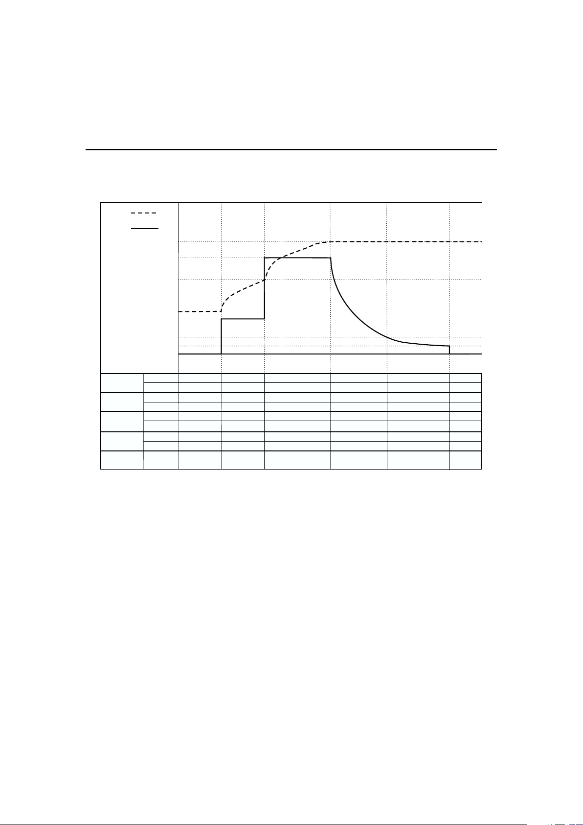
Charge Status Display
Charge status is indicated by the LED driver outputs
LED
1
–LED2. Three display modes (Tables 1– 3) are avail
able in the bq2954 and are selected by configuring pin
DSEL. Table 1 illustrates a normal fast charge cycle, Ta
ble 2 a recharge-after-fast-charge cycle, and Table 3 an ab
normal condition.
Configuring the Display Mode, I
FULL/IMIN
,
and I
SENSE
DSEL/LED
2
and CSEL/LED1are bi-directional pins
with two functions: as LED driver pins (output) and as
programming pins (input). The selection of pull-up,
pull-down, or no-resistor programs the display mode on
DSEL as shown in Tables 1 through 3. A pull-down or
no-resistor programs the current-sense mode on CSEL.
The bq2954 latches the programming data sensed on
the DSEL and CSEL input when V
CC
rises to a valid
level. The LEDs go blank for approximately 400ms (typi
-
cal) while new programming data are latched.
When fast charge reaches a condition where the charg
-
ing current drops below I
FULL
, the LED1 and LED2
outputs indicate a full-battery condition. Fast charge
terminates when the charging current drops below the
6
bq2954
GR295401.eps
V
BAT
I
BAT
V
REG
I
MAX
V
MIN
I
COND
I
FULL
I
MIN
Battery
Absent
Qualification
Charge
Complete
Low
Low
Low
Low
Low
Low
Low
High
Low
High
MTO
Fast Charge
Current
Regulate
LED1
LED2
LED1
LED2
LED1
LED2
CHG
BTST
CHG
BTST
High
Low
High
Low
High
Low
High
Low
High
High
High
Low
High
Low
High
Low
High
Low
High
Low
High
Low
High
Low
High
High
High
Low
High
Low
Low
High
Low
High
Low
High
High
Low
High
Low
Low
High
Low
High
Low
High
Low
Low
Low
Low
Mode 1
(DSEL = 0)
Mode 2
(DSEL = 1)
Mode 3
(DSEL = F)
Mode 1
and 2
Mode 3
Time
Voltage
Regulate
Current
Taper
I
FULL
Detect
Table 1. Normal Fast Charge Cycle
7
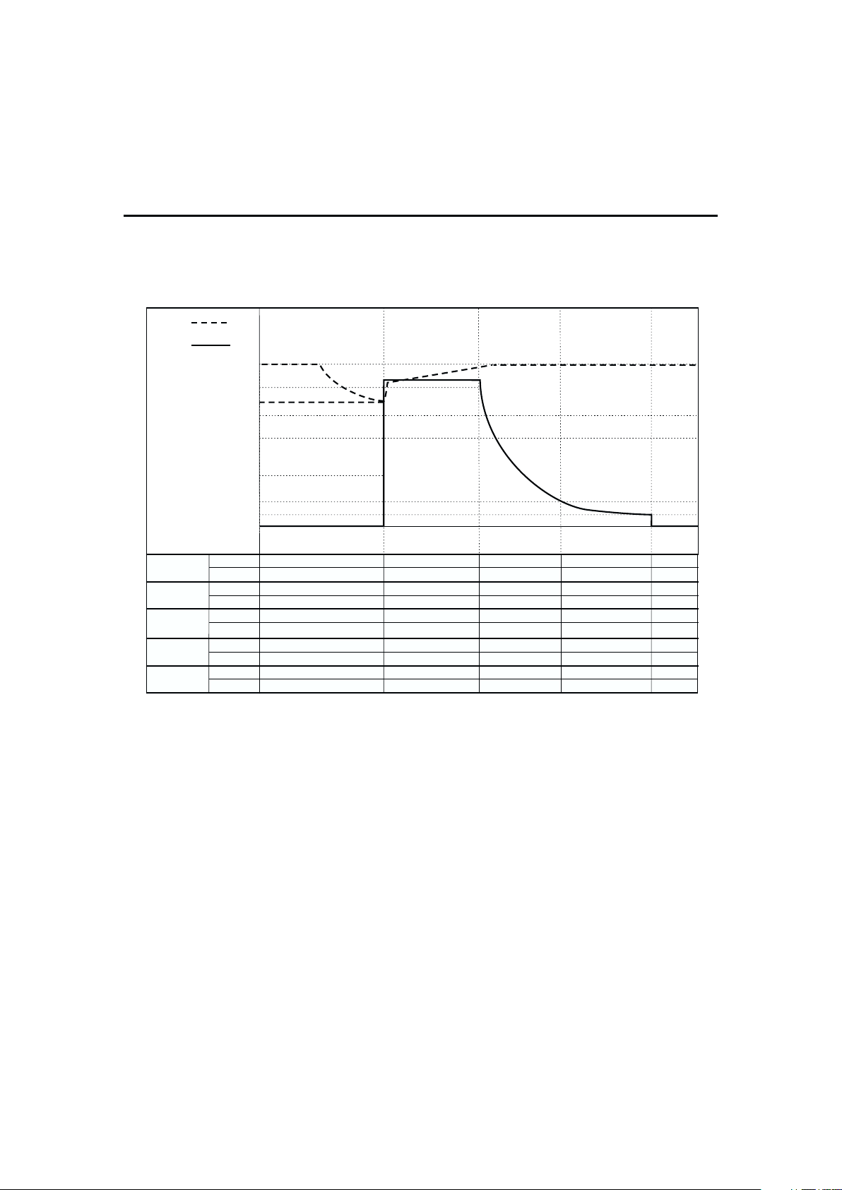
bq2954
Grbq295402.eps
V
BAT
I
BAT
V
REG
V
RECHG
I
MAX
V
MIN
I
COND
I
FULL
I
MIN
Charge Complete
Charge
Complete
MTO
Discharge
Fast Charge
Current
Regulate
LED1
LED2
LED1
LED2
LED1
LED2
CHG
BTST
CHG
BTST
High
Low
High
Low
High
Low
High
Low
High
Low
High
Low
High
Low
High
High
High
Low
High
Low
Low
High
Low
High
Low
High
High
Low
High
Low
Low
High
Low
High
Low
High
Low
Low
Low
Low
Low
High
Low
High
Low
High
Low
Low
Low
Low
Time
Voltage
Regulate
Current
Taper
I
FULL
Detect
Mode 1
(DSEL = 0)
Mode 2
(DSEL = 1)
Mode 3
(DSEL = F)
Mode 1
and 2
Mode 3
Table 2. Recharge After Fast Charge Cycle

8
bq2954
GR295403.eps
V
BAT
I
BAT
V
REG
I
MAX
V
MIN
I
COND
I
MIN
Battery
Absent
Qualification
Low
Low
Low
Low
Low
Low
Low
High
t
QT
LED1
LED2
LED1
LED2
LED1
LED2
High
Low
High
Low
High
Low
High
Low
Flash
Low
Low
Low
Low
Low
Low
Low
Mode 1
(DSEL = 0)
Mode 2
(DSEL = 1)
Mode 3
(DSEL = F)
CHG
BTST
Time
Abnormal
Battery
Table 3. Abnormal Condition
I
TERM
I
FULL
I
MIN
0I
MAX
/5 I
MAX
/10
1I
MAX
/10 I
MAX
/15
ZI
MAX
/15 I
MAX
/20
Table 4 . I
FULL
and I
MIN
Thresholds

minimum current threshold, I
MIN
. The I
FULL
and I
MIN
thresholds are programmed using the I
TERM
input pin
(See Table 4.)
Figures 4 and 5 show the bq2954 configured for display
mode 2 and I
FULL=IMAX
/5 while I
MIN=IMAX
/10.
Voltage and Current Monitoring
In low-side current sensing, the bq2954 monitors the
battery pack voltage as a differential voltage between
BAT and pins. In high-side current sensing, the bq2954
monitors the battery pack voltage as a differential volt
-
age between BAT and V
SS
pins. This voltage is derived
by scaling the battery voltage with a voltage divider.
(See Figures 6 and 7.) The resistance of the voltage di
vider must be high enough to minimize battery drain
but low enough to minimize noise susceptibility. RB1 +
RB2 is typically between 150kΩ and 1MΩ. The volt
age-divider resistors are calculated from the following:
RB1
RB2
NV
V
CELL
REG
=
∗
− 1
(1)
where
V
CELL
= Manufacturer-specified charging cell voltage
N = Number of cells in series
V
REG
= 2.05V
The current sense resistor, R
SNS
(see Figures 6 and 7),
determines the fast-charge current. The value of R
SNS
is given by the following:
R
V
I
SNS
MAX
=
025.
(2)
where I
MAX
is the current during the constant-current
phase of the charge cycle. (See Table 1.)
Battery Insertion and Removal
V
BAT
is interpreted by the bq2954 to detect the presence
or absence of a battery. The bq2954 determines that a
battery is present when V
BAT
is between the
High-Voltage Cutoff (V
HCO=VREG
+ 0.25V) and
the Low-Voltage Cutoff (V
LCO
= 0.8V). When V
BAT
is
outside this range, the bq2954 determines that no battery
is present and transitions to the battery test state, testing
for valid battery voltage. The bq2954 detects battery re
-
moval when V
BAT
falls below V
LCO
. The BTST pin is
driven high during battery test and can activate an exter
nal battery contact pull-up. This pull-up may be used to
activate an over-discharged Li-Ion battery pack. The V
HCO
limit implicitly serves as an over-voltage charge fault. The
CHG output can be used to disconnect capacitors from the
regulation circuitry in order to quickly detect a battery-re
moved condition.
Battery insertion is detected within 500ms. Transition
to the fast-charge phase, however, will not occur for time
t
HO
(approximately one second), even if voltage qualifi
-
cation V
MIN
is reached. This delay prevents a voltage
spike at the BAT input from causing premature entry
into the fast-charge phase. It also creates a delay in
detection of battery removal if the battery is removed
during this hold-off period.
Temperature Monitoring
Temperature is measured as a differential voltage be
tween TS and BAT-. This voltage is typically generated
by a NTC (negative temperature coefficient) thermistor
and thermistor linearization network. The bq2954 com
pares this voltage to its internal threshold voltages to
determine if charging is allowed. These thresholds are
the following:
■
High-Temperature Cutoff Voltage: V
TCO
= 0.4 ∗ V
CC
This voltage corresponds to the maximum temperature
(TCO) at which charging is allowed.
■
High-Temperature Fault Voltage: V
HTF
= 0.44 ∗ V
CC
This voltage corresponds to the temperature (HTF) at
which charging resumes after exceeding TCO.
■
Low-Temperature Fault Voltage: V
LTF
= 0.6 ∗ V
CC
This voltage corresponds to the minimum temperature
(LTF) at which charging is allowed.
Charging is inhibited if the temperature is outside the
LTF—TCO window. Once the temperature exceeds
TCO, it must drop below HTF before charging resumes.
RT1 and RT2 for the thermistor linearization network
are determined as follows:
061.
()
()
∗=
+
∗+
∗
V
V
RT1 RT2 R
RT2 R
CC
LTF
LTF
(3)
044
1
1
.
()
()
=
+
∗+
∗
RT1 RT2 R
RT2 R
HTF
HTF
(4)
where
R
LTF
= thermistor resistance at LTF
R
HTF
= thermistor resistance at HTF
V=V
CC
- 0.250 in low-side current sensing
V= V
CC
in high-side current sensing
TCO is determined by the values of RT1 and RT2. 1%
resistors are recommended.
9
bq2954

10
bq2954
LED2/DSEL
FGbq295402LS.eps
LED1
V
CC
V
SS
LCOM
bq2954
Low-Side Sense Mode
11
12
13
15
16
6
V
SS
V
CC
10K
1K
1K
Figure 4. Configured Display Mode
(Low-Side Sense)
LED2/DSEL
FGbq295402HS.eps
LED1
V
CC
V
SS
LCOM
bq2954
High-Side Sense Mode
11
12
13
15
16
6
V
SS
V
CC
10K
10K
1K
1K
Figure 5. Configured Display Mode
(High-Side Sense)
FGbq295403LS.eps
BAT
SNS
bq2954
7
3
13
V
CC
12
BAT +
BAT -
V
SS
R
SNS
RB2
RB1
V
SS
V
CC
Low-Side Sense Mode
Figure 6. Configuring the Battery Divider
(Low-Side Sense)
FGbq295403HS.eps
BAT
MOD
SNS
bq2954
7
3
13
V
CC
12
BAT +
BAT -
V
SS
R
SNS
RB2
RB3
RB1
V
SS
V
CC
High-Side Sense Mode
Current
Mirror
Switching
Circuit
Figure 7. Configuring the Battery Divider
(High-Side Sense)
Disabling Temperature Sensing
Temperature sensing can be disabled by placing a 10k
Ω
resistor between TS and BAT- and a 10kΩresistor between TS and V
CC
. See Figures 8 and 9.
Maximum Time-Out
Maximum Time-Out period (t
MTO)
is programmed from
1 to 24 hours by an R-C network on the TM pin (see Fig
-
ure 10) per the following equation:
tRC
MTO =∗∗500
(5)
where R is in ohms, C is in Farads, and t
MTO
is in hours.
The recommended value for C is 0.1µF.
The MTO timer is reset at the beginning of fast charge.
If the MTO timer expires during the voltage regulation
phase, fast charging terminates and the bq2954 enters
the Charge Complete state. If the conditioning phase
continues for time equal to tQT(MTO/4) and the battery
potential does not reach V
MIN
, the bq2954 enters the
fault state and terminates charge. See Table 3. If the
MTO timer expires during the current-regulation phase
(V
BAT
never reaches V
REG
), fast charging is terminated,
and the bq2954 enters the fault state.
11
bq2954
FGbq295404LS.eps
SNS
LPD1
bq2954
7
13
V
CC
12
BAT -
V
SS
R
SNS
RT2
RT1
V
SS
V
CC
TS
8
t
NTC
Thermistor
RT
Low-Side Sense Mode
Figure 8. Low-Side Temperature Sensing
FGbq295404HS.eps
LPD1
bq2954
13
V
CC
12
BAT -
V
SS
RT2
RT1
V
SS
V
CC
TS
SNS
8
7
NTC
Thermistor
R
CSEL
High-Side Sense Mode
Figure 9. High-Side Temperature Sensing
TM
FGbq295405.eps
V
CC
V
SS
bq2954
12
13
1
V
SS
V
CC
C
R
Figure 10. R-C Network/Setting MTO

Charge Regulation
The bq2954 controls charging through pulse-width
modulation of the MOD output pin, supporting both
constant-current and constant-voltage regulation.
Charge current is monitored at the SNS pin, and charge
voltage is monitored at the BAT pin. These voltages are
compared to an internal reference, and the MOD output
is modulated to maintain the desired value. The maxi
-
mum duty cycle is 80% .
Voltage at the SNS pin is determined by the value of re
-
sistor R
SNS
, so nominal regulated current is set by the
following equation:
I
MAX=VSNS/RSNS
(6)
The switching frequency of the MOD output is deter
mined by an external capacitor (CPWM) between the pin
TPWM and V
SS
pins, per the following:
f
C
PWM
PWM
=
∗
−
110
4
(7)
Where C is in Farads and the frequency is in Hz. A
typical switching rate is 100kHz, implying C
PWM
=
0.001µF. MOD pulse width is modulated between 0 and
80% of the switching period.
To prevent oscillation in the voltage and current control
loops, frequency compensation networks (C and R-C
respectively) are typically required on the V
COMP
and
I
COMP
pins .
Recharge After Fast Charge
Once charge completion occurs, a fast charge is initiated
when the battery voltage falls below V
RECHG
threshold.
A delay of approximately one second passes before re
charge begins so that adequate time is allowed to detect
battery removal. (See Table 1.)
12
bq2954

13
Absolute Maximum Ratings
Symbol Parameter Minimum Maximum Unit Notes
V
CC
VCCrelative to V
SS
-0.3 +7.0 V
V
T
DC voltage applied on any pin ex
-
cluding V
CC
relative to V
SS
-0.3 +7.0 V
T
OPR
Operating ambient temperature
-20 +70 °C Commercial
-40 +85 °C Industrial “N”
T
STG
Storage temperature -55 +125 °C
T
SOLDER
Soldering temperature - +260 °C 10s max.
Note: Permanent device damage may occur if Absolute Maximum Ratings are exceeded. Functional opera-
tion should be limited to the Recommended DC Operating Conditions detailed in this data sheet. Exposure to conditions beyond the operational limits for extended periods of time may affect device reliability.
DC Thresholds (T
A=TOPR;VCC
= 5V±10%)
Symbol Parameter Rating Unit Tolerance Notes
V
REG
Internal reference voltage 2.05 V 1% TA = 25°C
Temperature coefficient -0.5 mV/°C 10%
V
LTF
TS maximum threshold 0.6*V
CC
V
±
0.03V Low-temperature fault
V
HTF
TS hysteresis threshold 0.44*V
CC
V
±
0.03V High-temperature fault
V
TCO
TS minimum threshold 0.4*V
CC
V
±
0.03V Temperature cutoff
V
HCO
High cutoff voltage V
REG
+ 0.25V V
±
0.03V
V
MIN
Under-voltage threshold at BAT 1.5 V
±
0.05V
V
RECHG
Recharge voltage threshold at BAT 1.92 V
±
0.05V
V
LCO
Low cutoff voltage 0.8 V
±
0.03V
V
SNS
Current sense at SNS
0.250 V 10% I
MAX
0.025 V 10% I
COND
bq2954

14
bq2954
Recommended DC Operating Conditions (T
A=TOPR)
Symbol Parameter Minimum Typical Maximum Unit Notes
V
CC
Supply voltage 4.5 5.0 5.5 V
V
TEMP
TS voltage potential 0 - V
CC
VVTS-V
SNS
V
BAT
BAT voltage potential 0 - V
CC
V
I
CC
Supply current - 2 4 mA Outputs unloaded
I
IZ
DSEL tri-state open detection -2 - 2
µ
A Note
I
TERM
tri-state open detection -2 2
µ
A
V
IH
Logic input high VCC- 0.3 - - V DSEL, I
TERM
V
IL
Logic input low - - VSS+ 0.3 V DSEL, CSEL, I
TERM
V
OH
LED1, LED2, BTST, output high VCC- 0.8 - - V I
OH
≤
10mA
MOD output high V
CC
- 0.8 - - V I
OH
≤
10mA
V
OL
LED1, LED2, BTST, output low - - VSS+0.8 V I
OL
≤
10mA
MOD output low - - V
SS
+ 0.8 V I
OL
≤
10mA
CHG output low - - V
SS
+ 0.8 V I
OL
≤
5mA, Note 3
LCOM output low - - V
SS
+ 0.5 V I
OL
≤
30mA
I
OH
LED1, LED2, BTST, source -10 - - mA VOH=VCC- 0.5V
MOD source -5.0 - - mA V
OH=VCC
- 0.5V
I
OL
LED1, LED2, BTST, sink 10 - - mA VOL=VSS+ 0.5V
MOD sink 5 - - mA V
OL=VSS
+ 0.8V
CHG sink 5 - - mA V
OL=VSS
+ 0.8V, Note 3
LCOM sink 30 - - mA V
OL=VSS
+ 0.5V
I
IL
DSEL logic input low source - - +30
µ
AV=VSSto VSS+ 0.3V, Note 2
I
TERM
logic input low source - - +70
µ
AV =VSSto VSS+ 0.3V
I
IH
DSEL logic input high source -30 - -
µ
AV =VCC- 0.3V to V
CC
I
TERM
logic input high source -70 - -
µ
AV =VCC- 0.3V to V
CC
Notes: 1. All voltages relative to VSS.
2. Conditions during initialization after V
CC
applied.
3. SNS = 0V.
15
bq2954
Impedance (T
A=TOPR;VCC
= 5V±10%)
Symbol Parameter Minimum Typical Maximum Unit Notes
R
BATZ
BAT pin input impedance 50 - - M
Ω
R
SNSZ
SNS pin input impedance 50 - - M
Ω
R
TSZ
TS pin input impedance 50 - - M
Ω
R
PROG1
Soft-programmed pull-up or pull-down
resistor value (for programming)
--10
k
Ω
DSEL, CSEL
R
PROG2
Pull-up or pull-down resistor value - - 3 k
Ω
I
TERM
R
MTO
Charge timer resistor 20 - 480 k
Ω
Timing (T
A=TOPR;VCC
= 5V±10%)
Symbol Parameter Minimum Typical Maximum Unit Notes
t
MTO
Charge time-out range 1 - 24 hours See Figure 10
t
QT
Pre-charge qual test time-out period -
0.25 ∗ t
MTO
--
t
HO
Pre-charge qual test hold-off period 300 600 900 ms
f
PWM
PWM regulator frequency range - 100 200 kHz See Equation 7
d
PWM
Duty cycle 0 - 80 %
Capacitance
Symbol Parameter Minimum Typical Maximum Unit
C
MTO
Charge timer capacitor - - 0.1
µ
F
C
PWM
PWM capacitor - 0.001 -
µ
F
16
bq2954
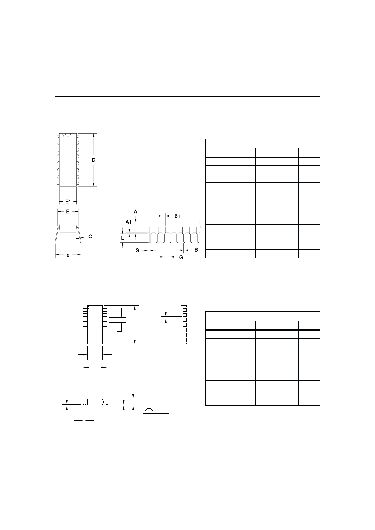
16-Pin PN(0.300" DIP
)
Dimension
Inches Millimeters
Min. Max. Min. Max.
A 0.160 0.180 4.06 4.57
A1 0.015 0.040 0.38 1.02
B 0.015 0.022 0.38 0.56
B1 0.055 0.065 1.40 1.65
C 0.008 0.013 0.20 0.33
D 0.740 0.770 18.80 19.56
E 0.300 0.325 7.62 8.26
E1 0.230 0.280 5.84 7.11
e 0.300 0.370 7.62 9.40
G 0.090 0.110 2.29 2.79
L 0.115 0.150 2.92 3.81
S 0.020 0.040 0.51 1.02
16-Pin DIP Narrow (PN)
16-Pin SOIC Narrow (SN)
A
A1
.004
C
B
e
D
E
H
L
16-Pin SN(0.150" SOIC
)
Dimension
Inches Millimeters
Min. Max. Min. Max.
A 0.060 0.070 1.52 1.78
A1 0.004 0.010 0.10 0.25
B 0.013 0.020 0.33 0.51
C 0.007 0.010 0.18 0.25
D 0.385 0.400 9.78 10.16
E 0.150 0.160 3.81 4.06
e 0.045 0.055 1.14 1.40
H 0.225 0.245 5.72 6.22
L 0.015 0.035 0.38 0.89

17
bq2954
Data Sheet Revision History
Change No. Page No. Description of Change
1 All “Final” changes from “Preliminary” version
Note: Change 1 = Oct. 1998 B changes from Nov. 1997 “Preliminary.”
Ordering Information
bq2954
Package Option:
PN = 16-pin plastic DIP
SN = 16-pin narrow SOIC
Device:
bq2954 Li-Ion Fast-Charge IC

18
IMPORTANT NOTICE
Texas Instruments and its subsidiaries (TI) reserve the right to make changes to their products or to discontinue any
product or service without notice, and advise customers to obtain the latest version of relevant information to verify,
before placing orders, that information being relied on is current and complete. All products are sold subject to the
terms and conditions of sale supplied at the time of order acknowledgement, including those pertaining to warranty,
patent infringement, and limitation of liability.
TI warrants performance of its semiconductor products to the specifications applicable at the time of sale in accor
dance with TI’s standard warranty. Testing and other quality control techniques are utilized to the extent TI deems
necessary to support this warranty. Specific testing of all parameters of each device is not necessarily performed, ex
cept those mandated by government requirements.
CERTAIN APPLICATIONS USING SEMICONDUCTOR PRODUCTS MAY INVOLVE POTENTIAL RISKS OF DEATH,
PERSONAL INJURY, OR SEVERE PROPERTY OR ENVIRONMENTAL DAMAGE (“CRITICAL APPLICATIONS”). TI
SEMICONDUCTOR PRODUCTS ARE NOT DESIGNED, AUTHORIZED, OR WARRANTED TO BE SUITABLE FOR
USE IN LIFE-SUPPORT DEVICES OR SYSTEMS OR OTHER CRITICAL APPLICATIONS. INCLUSION OF TI
PRODUCTS IN SUCH APPLICATIONS IS UNDERSTOOD TO BE FULLY AT THE CUSTOMER’S RISK.
In order to minimize risks associated with the customer’s applications, adequate design and operating safeguards
must be provided by the customer to minimize inherent or procedural hazards.
TI assumes no liability for applications assistance or customer product design. TI does not warrant or represent that
any license, either express or implied, is granted under any patent right, copyright, mask work right, or other intellec
tual property right of TI covering or relating to any combination, machine, or process in which such semiconductor
products or services might be or are used. TI’s publication of information regarding any third party’s products or ser
vices does not constitute TI’s approval, warranty or endorsement thereof.
Copyright © 1999, Texas Instruments Incorporated
 Loading...