

Page 1
DRV830x Rev D. Hardware Quick Start Guide
Version 1.0.5 Motor Solutions
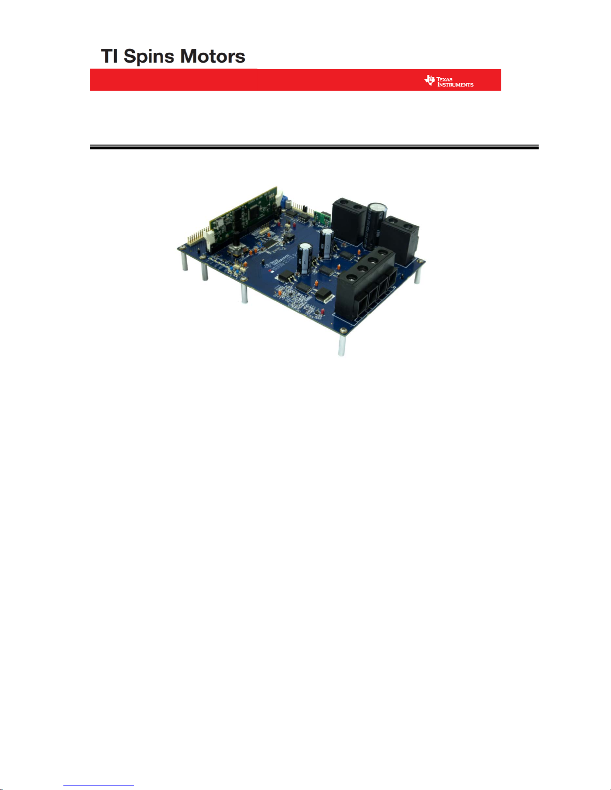
Fig 1: DRV830x EVM with controlCARD
Abstract
The Low Voltage, High C urrent Motor Drive EV M (DRV8301, F igure 1), provides a gr eat way to
learn and experiment with digital control of sub 60 volt three-phase motors to increase efficienc y
of operation. The bo ard is available in two conf igurations, the DRV8301 or the DRV8302. This
document goes over the typical kit contents and hardw are details, and explains t he functions and
locations of jumpers and connectors present on the board. This document supersedes all the
documents available for the kit.
1
Page 2
Version: 1.0.5
Revision History:
1.0.5 April 23, 2014 Fixed page 18-20 co mm ent s rega r di ng A DC
and IQ CURRENT, VOLTAGE, and pole settings
1.04 January 29, 2014 Changed page 8 regarding GPIO to Enable Pin
connection with TMDSCN C D 28027F
1.03 July 11, 2013 Updated for TMDSCNCD28027F support. See
specific instruction s o n Page 8.
Added section on Optimizing Sense Circuitry
1.0.2 March 21, 2013 Added Revision History
1.0.1 February 26,
2013
First release
2
Page 3
WARNING
This EVM is meant to be operated in a lab environment only and is not
considered by TI to be a finished end-product fit for gene ral consu mer u se
This EVM must be used only by qualified engineers and technicians familiar
with risks associated with handling high voltage electrical and
mechanical components, systems and subsystems.
This equipment operates at voltages and currents that can result in electrical shock, fire
hazard and/or personal injury if not properly handled or applied. Equipment must be used
with necessary caution and appropriate safeguards employed to avoid personal injury or
property damage.
It is the user’s responsibility to confirm that the voltages and isolation requirements are
identified and understood, prior to energizing the board and or simulation. When
energized, the EVM or components connected to the EVM should not be touched.
3
Page 4

Table of Contents
Getting Familiar with the Kit .......................................................................................................... 5
Kit Contents .............................................................................................................................................................................. 5
Board Features: ........................................................................................................................................................................ 5
Warning: about low switching frequencies on the DRV830x .................................................................................................... 5
Hardware Overview ........................................................................................................................ 6
Macro Blocks ............................................................................................................................................................................ 6
Powering the Board ......................................................................................................................... 8
Hardware Resource Mapping .......................................................................................................... 9
Resource Allocation .................................................................................................................................................................. 9
Jumpers and Connectors ........................................................................................................................................................ 11
Optimizing Sense Circuitry ........................................................................................................... 16
Overview ................................................................................................................................................................................. 16
Shunt Current Feedback ......................................................................................................................................................... 17
Phase Voltage Feedback ........................................................................................................................................................ 18
Phase Voltage Filter Feedback ............................................................................................................................................... 20
SCHEMATIC DISCLAIMER AND WARNINGS ...................................................................... 22
4
Page 5

Getting Familiar with the Kit
Kit Contents
The DRV830x EVM is usually available packaged as a full solution kit:
• MCU controlCARD
• DRV830x EVM board with slot for the controlCARD
• USB Cable
• USB/DVD with CCStudio IDE, GUI, documentation, and link to project software
distribution
• Some versions ship with a tabl etop 24V 2.5A power supply and 24V M otor with built-in
Hall Sensors and Encoder
The DRV830x EVM board can accept m any of the TI MCU controlCARDs, but we r ecommend
using the versions that ship with the kits that include the JTAG emulator, USB to serial, and
isolation on the controlCARD. It is recommended to always check for any updates to the GUI
executable and MCU program.
Board Features
:
The board has the following features
• Three-Phase Pow er Stage, DRV830x capable of driving 3-phase brushless DC motors
and Permanent Magnet Synchronous Motors.
o 60V DC max input voltage
o 60A peak output current per phase
o Up to 200khz driver switching frequency
o Integrated 1A buck converter to provide logic and analog power
o Dual integrated current sense amplifiers
• Isolated CAN and SPI communication (will only work if MCU supports and SW is
enabled)
• JTAG connector for external emulators
• Quadrature Encoder Interfa ce and Hall Sensor Interface availab le for speed and pos ition
measurement (only if MCU supports and SW is enabled)
• High precision low-side cur rent sensing using integrated curr ent sense amplifiers in the
DRV830x (2-ch) or optional external 3-ch (Starting with DRV8301 RevD)
• Over current protection on the inverter stage by DRV830x
• Hardware Developer’s Package that includes schematics and bill of materials
• Closed-loop digital control with feedback using the MCU’s on-chip PWM and ADC
peripherals
Warning: about low switching frequencies on the DRV830x
When the DRV830x runs at a low switching frequency (e.g. less than 20 kHz with 100 nF
bootstrap capacitor), the bootstrap capacitor voltage might not be able to maintain a proper
5
Page 6

voltage level for the high-side gate driver. A bootstrap capacitor under voltage protection circuit
(BST_UVP) will start under this circumstance to prevent the potential failure of the high-side
MOSFET. In this circumstance, both the FAULT and OTW pins should pull low and the device
should self-protect itself. The motor’s inductance and the inverter’s bootstrap cap ac itance will
allow the DRV830x to run efficiently until approximately 10 kHz (with margin). Setting the PWM
switching frequency below 10 kHz may cause issues on the inverter output and is not
recommended. Please reference the datasheet.
Hardware Overview
The example projects made available wit h th e kit may be done with a s up pl ied 24V power suppl y,
but many of the examples will work with an externally supplied laboratory power supply of a
different voltage or current limit. The DRV830x EVM has all the power and control blocks that
constitute a typical m otor drive system for a three-phase system : Communications + Control +
Feedback + Feedforward + Drive
Macro Blocks
The motor control board is separated into function al groups that enable a com plete motor drive
system, these are ref erred to as m acro blocks . Following is a list of the mac ro blocks pr esent on
the board and their functions:
• controlCARD socket – Socket for a controlCARD (preferably using built-in em ulation) .
• DC Bus Connection
o “PVDD/GND” Terminals – Connect an external 8-60V DC lab supply here
making sure to observe correct polarity..
• DRV830x – This module includes either the DRV8301 or DRV8302 Three Phase Pre-
Driver as well as all of the necessary external passive components.
• Current Sense – Low-side shunt current sensing on each half-bridge.
• Quadrature Encoder Connections – Connections are available for an optional shaft
encoder to interface to the MCU’s QEP peripheral.
• Hall Effect Sensor Connections – Connections are available for optional Hall Effect
Sensors.
Fig 2, illustrates the position of these macro blocks on the board. The use of a macro block
approach, for different po wer stages enables easy debug an d testing of one stage at a time. All
the PWM’s and ADC signals which are the actuation and sense signals have designated test
points on the board , which makes it eas y for an application d eveloper to try out new algorithms
and strategies.
6
Page 7
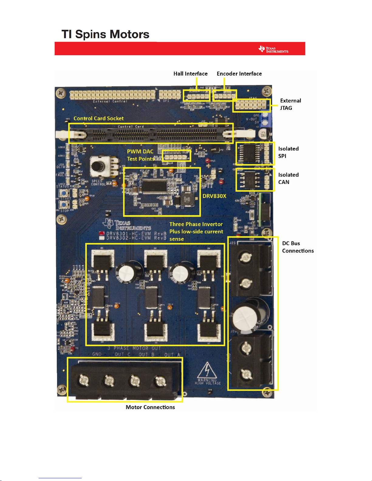
Fig2: DRV830x-EVM Board Macros
7
Page 8

Powering the Board
The board is separated int o two power domains*, the low volt age Controller Power domain that
powers the controller and t he logic circuit present on the board, and the medium voltage power
delivery line that is used to carry the medium voltage and current like the DC power for the
Inverter also referred to as DC Bus.
1) Controller Power comprises of the 5 V and 3.3V that t he board uses to power the controller
and the logic and sensi ng circuit present o n the board. This power is regulat ed from the DC bus
by the DRV830x integrated buck converter.
2) DC Bus Power is the medium voltage line – up to 60V - that provides the voltage to the
inverter stage to generate 3 phases to control the motor
Note: Do not apply power to board before you have verified these settings!
The kit ships with the control card inserted and the jumper and switch settings pre done
for connecting with the GUI. However the user must ensure that these settings are valid
on the board.
1. Make sure nothing is connected to the board, and no power is being supplied to
the board.
2. Insert the controlCARD into the connector if not already populated.
Special Notes Regarding controlCARD Use
• Make sure switches are set properly on the controlCARD according to the
appropriate qsg_hw_cncd280xxx.pdf
• Special notes for using controlCARDs with this motor drive board
o When using TMDSCNCD28027F
Connect pin 2 of J12 (GPIO-29) to pin 6 of J5 (EN_GATE).
Note, for all MotorWare versions up to _11 this was pin1 of
J11. Changed in _12 due to pin conflict.
3. Make sure the following jumpers & connector settings are valid i.e.
a. JP2 is installed
4. Connect your PC to the kit
a. controlCARDs with on-card XDS100 USB-JTAG:
i. connect USB cable from computer to USB connector on control
card
b. controlCARDs without on-card USB -JTAG
i. connect USB cable from comput er to external emulator, and
emulator to 14-pin JTAG header (J21)
5. Connect the motor you want to spin to the “MOTOR” terminal block as shown
below. The order is not important unless a rotor sensor is used. If ground is
available with your motor it should also be used.
8
Page 9

6. Connect an 8-60V DC power supply to the PVDD and GND terminals.
Fig3: DRV830x-HC-EVM Motor Connections
Hardware Resource Mapping
Resource Allocation
J1
Pin no.
GPIO Signal Name
Function
(DRV8301/DRV8302)
23 GPIO-00 PWM_AH DRV830x Phase AH PW M input
73 GPIO-01 PWM_AL DRV830x Phase AL PW M input
24 GPIO-02 PWM_BL DRV830x Phase BH PW M input
74 GPIO-03 PWM_BL DRV830x Phase BL PW M input
25 GPIO-04 PWM_CH DRV830x Phase CH PWM input
75 GPIO-05 PWM_CL DRV830x Phase CL PWM input
26 GPIO-06 DAC_PWM4 PWM DAC
76 GPIO-07 STOP Push button input
28 GPIO-08 DAC_PWM3 PWM DAC
78 GPIO-09 START Push button input
29 GPIO-10 DAC_PWM1 PWM DAC
79 GPIO-11 DAC_PWM2 PWM DAC
33 GPIO-12 LED-1 User LED
9
Page 10

83 GPIO-13 OCTWn Over-temperatur e warnin g
84 GPIO-14 FAULTn Over-current fault
34 GPIO-15 LED-2 User LED
38 GPIO-16 SPI-SIMO Isolated SPI Interface
88 GPIO-17 SPI-SOMI Isolated SPI Interface
39 GPIO-18 SPI-CLK Isolated SPI Interface
89 GPIO-19 SPI-STE Isolated SPI Interface
40 GPIO-20 QEPA Encoder A
90 GPIO-21 QEPB Encoder B
41 GPIO-22 STATUS User LED
91 GPIO-23 QEPI Encoder Index
35 GPIO-24 SDI SPI Data In/M_DC
85 GPIO-25 SDO SPI Data Out/GAIN
36 GPIO-26 SCLK SPI ClockDC_ADJ
86 GPIO-27 /SCS /SCS/M_PWM
44 GPIO-30 CAN-RX Isolated CAN Interface
94 GPIO-31 CAN-TX Isolated CAN Interface
30 GPIO-40 CAP1 Hall Input 1
80 GPIO-41 CAP2 Hall Input 2
31 GPIO-42 CAP3 Hall Input 3
81
59 ADC-A1 IA-FB Current sense phase A
61 ADC-A2 I-TOTAL DC Bus current sense
63 ADC-A3 IC-FB Current sense phase C
GPIO-43 DC-CAL
Short DC current sense amplifier
inputs to ground, calibrate offset
67 ADC-A5 IC-FB Current sense phase C
10
Page 11

71 ADC-A7 ADC-Vhb2 Phase Voltage sense B
7 ADC-B0 TSI Tach/Pot input
9 ADC-B1 IB-FB Current sense phase B
11 ADC-B2 VDCBUS DC Bus voltage sense
13 ADC-B3 IA-FB Current sense phase A
15 ADC-B4 ADC-Vhb3 Phase Voltage sense C
17 ADC-B5 IB-FB Current sense phase B
21 ADC-B7 ADC-Vhb1 Phase Voltage sense A
Table 1: Signal mapping to the controlCARD DIMM slot
Jumpers and Connectors
The Tables below show the various connections available on the board.
Connector Reference # of Pins Name
J2 2 HEADER2x1
J4 5 HEADER5x1
J5 40 HEADER20x2
J6 5 HEADER5x1
J7 3 HEADER3x1
J8 5 HEADER5x1
J10 5 HEADER5x1
TERM BLOCK HEADER
J11 4
J12 2 HEADER2x1
J13 2 HEADER2x1
J20 10 HEADER5x2
4x1
J21 14 HEADER7x2
11
Page 12

J23 2 HEADER2x1
J24 2 HEADER2x1
TERM BLOCK HEADER
J25 2
J26 2
Table 2: List of Connecto rs
2X1
TERM BLOCK HEADER
2X2
12
Page 13

13
J2 (User Power Access) J8 (User SPI)
Pin # Signal
1 VCC_5V 1 iSD-O 1 VCC_3.3V 1 TMS
2 GND 2 iCLK-O 2 GND 2 TRSTn
3 iSD-I 3 TDI
J4 (Optional Encoder)
Pin # Signal
1 E1A 1 NC 6 NC
2 E1B
3 E1C
4 VCC_5V 1 E2A 4 NC 9 TCK
5 GND 2 E2B 5 SDO 10 GND
3 E2C 6 NC 11 TCK
Pin # Signal
4 iGPIO
5 IGND
J10 (HALL Sensor)
Pin # Signal
J13 (User Power Access) J21 (External JTAG)
Pin # Signal
J20 (DRV8301 SPI))
Pin # Signal
2 GND 7 TDO
3 NC 8 GND
Pin # Signal
4 GND
5 VCC_3.3V
J6 (PWM DAC)
Pin # Signal
1 DAC1 9 /SCS 14 EMU1
2 DAC2
3 DAC3
4 DAC4 1 Phase A
5 GND 2 Phase B
3 Phase C 1 START 2 PVDD
J7 (CAN)
Pin # Signal
4 GND 2 GND
1 CAN-H
2 CAN-L
3 IGND 1 GPIO-28 1 STOP 2 GND
4 VCC_5V 7 SCLK 12 GND
5 GND 8 SDI 13 EMU0
J11 (Motor)
Pin # Signal
J12 (GPIO/SCI)
Pin # Signal
10 GND
J23 (Push Button)
Pin # Signal
J24 (Push Button)
Pin # Signal
J25 (Power Input)
Pin # Signal
1 PVDD
J26 (Power Input)
Pin # Signal
1 GND
2 GPIO-29 2 GND
Page 14

14
Tables3-17 Individual Connector Pinouts
J5 (External Controller Ac ces s )
Pin # Signal Pin # Signal
1 VCC_5V 2 VCC_5V
3 GND 4 GND
5 STATUS 6 EN_GATE
7 QEPA 8 QEPI
9 FAULTn 10 QEPB
11 CAP3 12 OCTWn
13 DC_CAL 14 CAP1
15 DAC_PWM1 16 CAP2
17 DAC_PWM3 18 DAC_PWM2
19 GND 20 GND
21 DACE_PWM4 22 PWM_CL
23 PWM_AL 24 PWM_BL
25 PWM_AH 26 PWM_CH
27 GND 28 PWM_BH
29 ADC-Vhb1 30 GND
31 ADC-Vhb2 32 ADC-Vhb3
33 IC-FB 34 VDCBUS
35 I_TOTAL 36 IB-FB
37 IA-FB 38 TSI
39 GND 40 GND
Table 18: J5 Pinout
Page 15

15
Test Points
Test Point Net Connection
TP1 VCC_5V JP2 VCC_5V to controlCARD
TP2 VCC_5V_R5 JP4 CAN termination
TP3 PWRGD
TP4 VCC_3.3V
TP5 REF_1.65V
TP6 PVDD
TP7 GND
TP8 GND
TP9 GND
TP10 GND
TP11 VCC_5V
Jumpers
Reference Function
TP12 SH_A
TP13 SH_B
TP14 SH_C
TP15 S02
TP16 IB-FB
TP17 IA-FB
TP18 U10_1
TP19 IC-FB
TP20 IGND
TP21 S01
TP22 U11_1
TP23 I-TOTAL
Table 20: Testpoints and Jumpers
Page 16

16
Optimizing Sense Circuitry
Overview
Proper resolution of motor signals is critical to the performance of any control system, but especially those
with software observers attempting to replace the precision of an absolute encoder. Because the
DRV83xx are built to work at over 50 Vdc-bus, the resolution of the voltage sensing is not as precise as
you would like for motors < 48V. And in the case of the DRV8301 which measures 41.25A, the current
resolution may also be unacceptable. This section describes how to update both the hardware and
corresponding software to maximize resolution and performance.
Steps to follow
1. Determine MAXIMUM phase current, adjust current gain to 3.3V ADC
2. Set MAX voltage at +30% margin of motor voltage, adjust voltage gain to 3.3V ADC
3. Configure software to hardware changes
Page 17

17
Shunt Current Feedback
=
1.65
=
3.3 1.65
10 0.01
= 16.5
= 16.5 = 16.5 k with = 1 k
= 1.65 +
Select resistor values to provide Vout = 3.3V for maximum peak-to-peak phase current
• Ex: For a maximum of 10A, consider a 0.01Ω shunt resistor
o One possible solution
Page 18

18
o Update the current hardware resistors
o
o
o
= R80, R81, R82
= R107, R95; R108,R105; R113, R103
= R92, R94; R101, R104; R99, R102
• Update your software settings in user.h; for this example of +/- 10A peak
//! \brief Defines the maximum current at the input to the AD converter
# USER_ADC_FULL_SCALE_CURRENT_A (20.0)
Insure that your IQ variable is >= 0.5 * the ADC value
# USER_IQ_FULL_SCALE_CURRENT_A (10.0)
Phase Voltage Feedback
Page 19

19
=
(
4.99 k+
)
4.99 k
15.6 = 3.3 V
(
4.99 k+
)
4.99 k
=
15.6 V 4.99 k
3.3 V
4.99 k = 18.6 k
• Ex: for a maximum of 12V, add headroom of 30% to set
o Update the voltage hardware resistors
to 15.6V
o
o = R62; R64; R65
o Update your software settings in user.h; for this example of 15.6V maximum
= R60; R61; R63
//! \brief Defines the maximum voltage at the input to the AD converter
# USER_ADC_FULL_SCALE_VOLTAGE_V (15.6)
In general an IQ value equal to your Voltage bus is effective.
During motor identification – for very small flux motors - you may need to make this value
smaller to lower the minimum flux value that can be identified, which is given by:
USER_IQ_FULL_SCALE_VOLTAGE_V / Effective Estimator Hz / 0.7
After motor identification - for larger flux motors - you may need to increase this value to
insure that the following is true:
USER_IQ_FULL_SCALE_VOLTAGE_V > USER_MOTOR_RATED_FLUX *
Maximum_Frequency_Hz (this is the maximum speed you will ever run the motor,
including deep field weakening).
# USER_IQ_FULL_SCALE_VOLTAGE_V (12.0)
Page 20

20
Phase Voltage Filter Feedback
_
=
=
_
= 400 =
1
2
18.6k 4.99 k
18.6k+ 4.99 k
C
v
• See 5.2.4 of the User’s Guide
• The voltage filter pole is needed by the FAST estimator to allow an accurate detection of the
voltage feedback. The filter should be low enough to filter out the PWM signals, and at the same
time allow a high speed voltage feedback signal to pass through the filter
• This pole should be designed to fall between
200 Hz <= Pole <= USER_IQ_FULL_SCALE_FREQ_Hz / 4 [hard upper limit]
o Higher poles are more sensitive to capacitor error and drift, so please recognize
the trade-offs in using a higher pole, especially for high frequency motors
• Example
o 4 pole pairs; 5 kRPM
Hz = RPM * Poles / 120 = 5000 * 8 / 120 = 333 Hz
Select 400 Hz (> 333 Hz)
o With our previous
=101
o
• Update the hardware capacitors
C
= C67; C68; C69
o
• Update your software settings in user.h
=4.99 kΩ ;
= =18.6 kΩ
Page 21

21
//! \brief Defines the analog voltage filter pole location, Hz
# USER_VOLTAGE_FILTER_POLE_Hz (400.0)
Page 22

22
SCHEMATIC DISCLAIMER AND WARNINGS
TI provides the DRV830x EVM schemati c drawi ngs to hel p users dev elop DRV30x & TI MCU
based reference design products. Application safety, safety of th e Medi um Voltage DMC kit
and design integrity of such reference designs are solely responsibility of the user. Any
reference d esign s generated off these schematics must take into account necessary product
safety design requirements, including interface components and load motors in order to
avoid user risks including potential for fire hazard, electrical shock hazard and personal
injury, including considerations for anticipated agency certification compliance
requirements.
Such product safety design criteria shall include but not be limited to critical circuit
creepages and clearances, component selection, ratings compatibility of controlled motor
loads, and required protective means (ie output fusing) depending on the specific loads
being controlled.
TI accepts no responsibility for design integrity of any reference designs based on supplied
schematic drawings and the schematics are strictly for development purposes.
EVALUATION BOAR D/KIT IMPORTANT NOTICE
Texas Instruments (TI) provides the enclos ed product(s) under the following conditions:
This evaluation board/kit is intended for use for ENGINEERING DEVELOPMENT,
DEMONSTRATION, OR EVALU ATION PURPOSES ONLY and is not considered by TI to
be a finished end-product fit for general consumer use. Persons handling the product(s)
must have electronics training and observe good engineering practice standards. As such,
the goods being provided are not intended to be complete in terms of required design-,
marketing-, and/or manufacturing-related protective considerations, including product
safety and environmental measures typically found in end products that incorporate such
semiconductor c omponents or circuit boards. This evaluation board/kit does not fall within
the scope of the European Union directives regarding electromagnetic compatibility,
restricted substances (RoHS), recycling (WEEE), FCC, CE or UL, and therefore may not meet
the technical requirements of these directives or other related directives.
Should this evaluation board/kit not meet the specifications indicated in the User’s Guide,
the board/ki t may be returned within 30 days from th e date of delivery for a full refund.
THE FOREGOING WARRANTY IS THE EXCLUSIVE WARRANTY MADE BY SELLER TO BUYER
AND IS IN LIEU OF ALL OTHER WARRANTIES, EXPRESSED, IMPLIED, OR STATUTORY,
INCLUDING ANY WARRANTY OF MERCHANTABILITY OR FITNESS FOR ANY PARTICULAR
PURPOSE.
The user assumes al l responsibility and liability for proper and safe handling of the goods.
Further, the user indemnifies TI from all claims arising from the handling or use of the
goods. Due to the open construction of the product, it is the user’s responsibility to take any
and all appropriate precautions with regard to electrostatic discharge.
EXCEPT TO THE EXTEN T OF THE INDE MNITY S ET FORTH AB OVE, NE ITHER PARTY S HALL BE
LIABLE TO THE OTHER FOR ANY INDIRECT, SPECIAL, INCIDENTAL, OR CONSEQUENTIAL
DAMAGES.
TI currentl y deals with a vari ety of customers for products, an d therefore our a rrangement
with the user is not exclusive.
Page 23

23
TI assumes no liability for applications assistance, customer product design,
software performance, or infringement of patents or services described herein.
Please read the U ser’s Guide and, specifi cally, the Warnings and R estrictions notice in th e
User’s Guide prior to handling the product. This notice contains important safety information
about temperatures and voltages. For additional information on TI’s environmental and/or
safety programs, please contac t the TI appl ication engineer or visit www.ti.com/esh.
No license is granted under any patent right or other intellectual property right of TI
covering or relating to any machine, process, or combination in which such TI products or
services might be or are used.
Mailing Address:
Texas Instrum en t s
Post Office Box 655303
Dallas, Texas 75265
Copyright © 2012, Texas Instrum en t s Incorporat ed
FCC Warning
This evaluation board/kit is intended for use for ENGINEERING DEVELOPMENT,
DEMONSTRATION, OR EVALUATION PURPOSES ONLY and is not considered by TI to
be a finished end-product f it for general consumer us e. It generat es, uses, and can radiat e
radio frequency energy and has not been tested for compliance with the limits of computing
devices pursuant to part 15 of FCC rules, which are designed to provide reasonable
protection against radio frequency interference. Operation of this equipment in other
environment s may caus e interfer ence with radio commun icati ons, in whi ch case the user at
his own expen se wil l b e requi red t o take whatever mea su res m ay be r equ ired to cor rect th i s
interference.
Page 24

IMPORTANT NOTICE
Texas Instruments Incorporated and its subsidiaries (TI) reserve the right to make corrections, enhancements, improvements and other
changes to its semiconductor products and services per JESD46, latest issue, and to discontinue any product or service per JESD48, latest
issue. Buyers should obtain the latest relevant information before placing orders and should verify that such information is current and
complete. All semiconductor products (also referred to herein as “components”) are sold subject to TI’s terms and conditions of sale
supplied at the time of order acknowledgment.
TI warrants performance of its components to the specifications applicable at the time of sale, in accordance with the warranty in TI’s terms
and conditions of sale of semiconductor products. Testing and other quality control techniques are used to the extent TI deems necessary
to support this warranty. Except where mandated by applicable law, testing of all parameters of each component is not necessarily
performed.
TI assumes no liability for applications assistance or the design of Buyers’ products. Buyers are responsible for their products and
applications using TI components. To minimize the risks associated with Buyers’ products and applications, Buyers should provide
adequate design and operating safeguards.
TI does not warrant or represent that any license, either express or implied, is granted under any patent right, copyright, mask work right, or
other intellectual property right relating to any combination, machine, or process in which TI components or services are used. Information
published by TI regarding third-party products or services does not constitute a license to use such products or services or a warranty or
endorsement thereof. Use of such information may require a license from a third party under the patents or other intellectual property of the
third party, or a license from TI under the patents or other intellectual property of TI.
Reproduction of significant portions of TI information in TI data books or data sheets is permissible only if reproduction is without alteration
and is accompanied by all associated warranties, conditions, limitations, and notices. TI is not responsible or liable for such altered
documentation. Information of third parties may be subject to additional restrictions.
Resale of TI components or services with statements different from or beyond the parameters stated by TI for that component or service
voids all express and any implied warranties for the associated TI component or service and is an unfair and deceptive business practice.
TI is not responsible or liable for any such statements.
Buyer acknowledges and agrees that it is solely responsible for compliance with all legal, regulatory and safety-related requirements
concerning its products, and any use of TI components in its applications, notwithstanding any applications-related information or support
that may be provided by TI. Buyer represents and agrees that it has all the necessary expertise to create and implement safeguards which
anticipate dangerous consequences of failures, monitor failures and their consequences, lessen the likelihood of failures that might cause
harm and take appropriate remedial actions. Buyer will fully indemnify TI and its representatives against any damages arising out of the use
of any TI components in safety-critical applications.
In some cases, TI components may be promoted specifically to facilitate safety-related applications. With such components, TI’s goal is to
help enable customers to design and create their own end-product solutions that meet applicable functional safety standards and
requirements. Nonetheless, such components are subject to these terms.
No TI components are authorized for use in FDA Class III (or similar life-critical medical equipment) unless authorized officers of the parties
have executed a special agreement specifically governing such use.
Only those TI components which TI has specifically designated as military grade or “enhanced plastic” are designed and intended for use in
military/aerospace applications or environments. Buyer acknowledges and agrees that any military or aerospace use of TI components
which have not been so designated is solely at the Buyer's risk, and that Buyer is solely responsible for compliance with all legal and
regulatory requirements in connection with such use.
TI has specifically designated certain components as meeting ISO/TS16949 requirements, mainly for automotive use. In any case of use of
non-designated products, TI will not be responsible for any failure to meet ISO/TS16949.
Products Applications
Audio www.ti.com/audio Automotive and Transportation www.ti.com/automotive
Amplifiers amplifier.ti.com Communications and Telecom www.ti.com/communications
Data Converters dataconverter.ti.com Computers and Peripherals www.ti.com/computers
DLP® Products www.dlp.com Consumer Electronics www.ti.com/consumer-apps
DSP dsp.ti.com Energy and Lighting www.ti.com/energy
Clocks and Timers www.ti.com/clocks Industrial www.ti.com/industrial
Interface interface.ti.com Medical www.ti.com/medical
Logic logic.ti.com Security www.ti.com/security
Power Mgmt power.ti.com Space, Avionics and Defense www.ti.com/space-avionics-defense
Microcontrollers microcontroller.ti.com Video and Imaging www.ti.com/video
RFID www.ti-rfid.com
OMAP Applications Processors www.ti.com/omap TI E2E Community e2e.ti.com
Wireless Connectivity www.ti.com/wirelessconnectivity
Mailing Address: Texas Instruments, Post Office Box 655303, Dallas, Texas 75265
Copyright © 2015, Texas Instruments Incorporated
 Loading...