

Page 1
TEAC
FD-55AV/
GV
MINI FLEXIBLE DISK DRIVE
MAINTENANCE
MANUAL
REV.
A
Page 2

MINI
TEAC
FD-5SAV~GV
=~XI3LE
DISK
DRl~JE
H.~INTI:N;'_~G
P.Jl..NU;lL
- i -
Page 3

TABLE
OF
CONTENTS
SECTION 3
3-1
CONSTRUCTION
3-1-1
3-1-2
3-2
3-2-1
General
Mechanical
CIRCUIT
Read
3-2-1-1
3- 2-1- 2
3-2-1-3
3-2-1-4
3-2-1-5
3-2-2
Control
3-2-2-1
3-2-2-2
3-2-2-3
THEORY
OF
Block
DESCRIPTIONS
Write
Mode
selector
Re
a d c
ireuit.
Writecircui
Low
voltage
Function
Circui
Strap
LED
and
circui
head
Write/erase
Title
OPERATION
AND
FUNCTION
Diagram
Section
Circuit
(for
. . . . . . . . . . . . . . . . . . . . . . . . . . . . . . . . . . . . . . . . . . . . . . .
t
.....•...........................................
sensor
and
operating
t
t
load
control
read
control
circuit
write
waveform
circuit
circuit)
of
read
......•......................
write
LSI
_
terminals
..
Page
300
301
301
302
307
307
309
311
315
317
318
326
328
329
333
3-2-2-4
3-2-2-5
3-2-2-6
3-2-2-7
3-2-2-8
3-2-2-9
3-2-3
3-3
3-3-1
3-3-2
Mc>tor
Ready
Stepping
Track
Other
Interface
Servo
Circuit
FUNCTION OF
Function
Function
on
gate
detector
motor
counter
terminals
driver
TEST
of
Test
of
Variable
...........................................•.....
control
and
POINTS
circuit
function
AND VARIABLE
of
control
RESISTORS
Points
Resistors
LSI
335
336
339
343
344
346
347
3~8
349
354
-
ii
-
Page 4

Title
Page
SECTION 4
4
-1
4-1-1
4-1~2
4-1-3
4-2
4-2-1
4-2-2
4-2-3
4-2-4
4-2-4-1
4-2-4-2
4-2-4-3
4-2-4-4
4-2-4-5
4-2-4-6
MAINTENANCE
GENERAL.............
Periodic
Check
Maintenance
and
Adjustment
Maintenance
........................•.........................
. . . . . . . . . . . . . . . . . . . . . . . . . . . . . . . . . . . . . . . . . . . ...4001
.'
Jigs
and
Tools
PRECAUTIONS...............................................
Torque
Handling
Head
Initial
Applied
Cable
Setting
Cable
connection
Setting
Setting
Level
disk
Alignment
of
Connectors
Treatment
of
of
disk
to
Screws
of
SKA-G
and
the
maximum
step
rate
calibration
calibration
Humiditysetting
and
and
setting
track
and
Locking
SKA
of
number
settling
Paint
power
time
supply
.~
•.....................
voltage
4000
4001
4002
4003
. . . . . ...4007
4007
4008
4013
4015
4015
4018
4018
4021
4023
4026
4
-2 -4
4-2-4-8
4-2-5
4-3
4-3-1
4-3-2
4-4
4-4-1
4-4-2
4-4-3
4-4-3-1
4-4-3-2
4-4
-4
4-4-5
4-4-6
4-4-7
- 7
Setting
Setting
Others
PREVENTIVE
Cleaning
Direct
CHECK
AND
Adjustment
Check
Check
and
and
[)()uble
Single
Check
of
Check
Check
of
Check
0 f
SKA
of
FDD
MAINTENANCE
of
Magnetic
Cleaning
ADJUSTMENT
of
Adjustment
Adjustment
sided
sided
CSS
Ass'
of
File
Disk
of
Erase
gain
Set
straps
<Single
Arm
and
Head
sided}
Position
of
Holder
of
Arm
SKA
by
Lifter
special
Cleaning
Position
key
Disk
....•....................
Y -.f054
Protect
Rotation
Gate
Sensor
Delay
............•.......................
Speed
4026
4027
4029
4032
4032
4034
4036
4036
4038
4041
4041
4051
4058
4061
4063
4-4-8
Check
of
Head
Touch
4066
-
iii
-
Page 5
Title
Page
4-4-9
4-4-10
4-4-11
4-4-12
4-4-13
4-4-14
4-4-15
4-5
4-5-1
4-5-1-1
4-5-1-2
4-5-2
4-5-3
4-5-4
4-5-5
4-5-6
Check
MAINTENANCE
Replacement
Replacement
Replacement
Replacement
Replacement
Replacement
and
Check
Check
Check
Check
Check
Check
of
of
and
and
and
and
Replacement
Replacement
Adjustment
Read
Level
Resolution
Adjustment
Adjustment
Adjustment
Adjustment
PARTS
REPLACEMENT
of
Head
of
of
of
Stepping
of
DD
of
Collet
of
Head
of
Track
Carriage
v-type
L-type
motor
Load
of
Asymmetry
of
of
of
of
carriage
carriage
MQtor
Ass'y
Ass'y
00
Sensor
Track
Track
Track
Index
Ass'y
Solenoid
Alignment
00
Sensor
00
Stopper
Burst
Ass
<Spindle
Ass'y
Timing
........................•.....
'y
motor},
........•......................
.........................
........................
.......................
.....................
4072
4077
4080
4084
4093
4100
4105
4110
4110
4110
4117
4121
4124
4126
4127
4129
4-5-7
4-5-8
4-5-9
4-5-10
4-5-11
4-5-12
Replacement
Replacement
Replacement
Replacement
Replacement
Replacement
of
of
of
of
of
of
PCBA
PCBA
Front
Front
CSS
Head
MFD
Front
Bezel
Lever
Ass'y
Pad
Control
OPT
Ass'y
(Single
#H
Ass'y
#H
sided)
.........•................
4130
4132
4133
4134
4135
4136
-
iv
-
Page 6

SECTION 3
THEORY
OF
OPERATION
-
300
-
Page 7
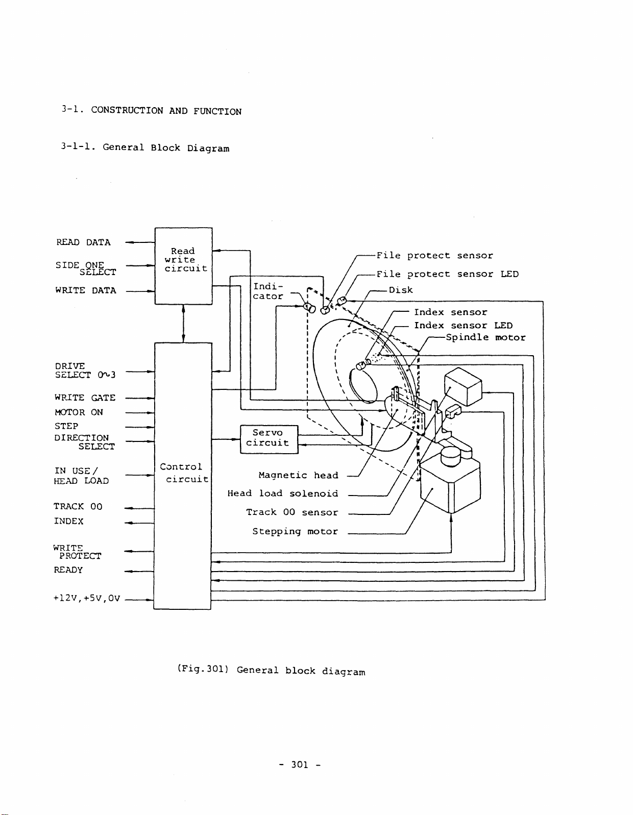
3-1.
CONSTRUCTION
AND
FUNCTION
3-1-1.
READ
DATA
SIDE
QNE
SeLECT
WRITE
DATA
DRIVE
Sc.:LECT
WRITE
MOTOR
STEP
()'\..3
GATE
ON
DIRECTION
SELECT
General
Block
write
circuit
Read
Diagram
Indi-
cator
Servo
circuit
File
protect
Index
Index
sensor
sensor
sensor
sensor
Spindle
LED
LED
motor
IN
USc.:
HEAD
TRACK
/
LOAD
00
INDEX
WRITE
PROTECT
READY
+12V,+SV,OV
Cunt.rol
circuit
(Fig.30l)
Head
General
Magnetic
load
Track
Stepping
solenoid
00
sensor
block
head
motor
diagram
-
301
-
Page 8
3-1-2.
Mechanical
Section
(1)
Since
and
the
data
mechanical
assembled
technicians
impact
The
mechanical
clamp
head
mechanism,
load
detection
Frame
The
main
circuit
the
stability
expansion
disk
is
interchangeability
section
carefully
can
handle
nor
drop
the
section
mechanism
mechanisms,
structure
boards.
of
coefficient.
a
disk
The
the
flexible
of
the
and
FDD
rotation
(or
etc.
for
frame
FDD
between
FDD
precisely.
the
internal
down
is
constructed
CSS
mechanism),
mounting
is
in
recording
uses
on
the
mechanism,
the
made
strength,
media
disks
precision
For
this
mechanism.
desk.
with
head
various
of
aluminum
precision,
made
and
FDDs
parts
reason,
frame,
magnetic
seek
mechanisms
of
is
and
Never
door
head
mechanism,
diecast
durability,
mylar
required,
it
only
apply
mechanism,
and
and
to
film
is
also
trained
excessive
carriage,
various
printed
maintain
and
base
the
disk
(2)
(3)
Door
The
door
forms
of
front
of
the
which
When a
inserted
the
Disk
The
mechanism
mechanism
the
structure
lever,
frame
forms
disk
into
correct
rotation
disk
rotation
and
clamp
with
the
disk
is
inserted
the
position
mechanism
disk
clamp
is
constructed
for
installing
arm,
leaf
spring
clamp
and
center
along
mechanism
mechanism
etc.
and
mechanism,
the
hole
of
the
comprises
outer
-
with
The
door
the
302
the
the
disk
set
on
the
is
is
disk
circumference
DO
-
main
on
arm
tip
attached.
closed,
and
motor
is
of
the
parts
the
attached
the
the
disk
Ass'y
of
spindle;
set
collet
is
of
the
which
set
arm
which
other
to
the
rear
armacollet,
is
clamped
collet.
includes
parts
in
Page 9
spindle.
The
DO
long
The
rotation
and
is
motor
life
maintained
of
is
an
30,000
speed
outor-rotor
hours
is
300rpm
at
a
stable
or
type
more
for
A
condition
DC
in
continuous
~
F
brushless
models
against
rotation.
or
load
motor
360rpm
which
for
variations
has
G
the
model
and
environmental
internal
The
center
and
position.
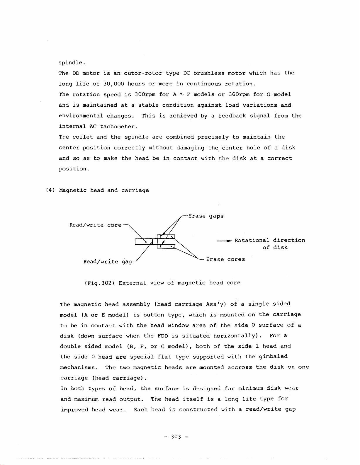
(4)
Magnetic
collet
position
so
as
Read/wri
(Fig.302)
AC
tachometer.
and
to
head
te
changes.
the
correctly
make
and
core
spindle
the
head
carriage
External
This
is
are
without
be
in
view
achieved
combined
damaging
contact
of
magnetic
by
a
precisely
the
with
gaps
Erase
head
feedback
center
the
___
cores
core
to
disk
Rota
signal
maintain
hole
at
tional
of
a
of
from
the
a
correct
direction
disk
the
disk
The
magnetic
model
to
disk
double
the
be
(A
in
(down
sided
side
mechanisms.
carriage
In
both
and
maximum
improved
or
contact
surface
0
head
(head
types
head
head
E
model)
model
The
of
read
wear.
assembly
with
when
(B,
are
special
two
carriage).
head,
output.
is
button
the
head
the
F,
or
magnp.tic
the
The
Each
head
(head
type,
window
FDD
G
model),
flat
heads
surface
head
-
carriage
is
type
is
constructed
303
which
area
situated
both
supported
are
is
designed
itself
-
Ass'y)
is
of
horizontally).
of
mounted
is
of
mounted
the
the
with
accross
for
a
long
with
a
single
on
side
side
the
iltinimWii
life
a
read/write
the
0
surface
1
head
gimbaled
the
type
sided
carriage
For
disk
disk
for
a
and
wear
of
on
gap
a
one
Page 10
used
for
data
reading
and
data
writing
and
two
erase
gaps
to
erase
the
(5)
recorded
The
magnetic
and
is
Head
The
head
the
CSS
solenoid.
The
head
disk
This
If
the
attached
the
side
track
specially
load
mechanism
load
mechanism
load
when
only
mechanism
head
to
1
surface
edge
ehad
assembled
mechanism
mechanism
required
is
loading
the
pad
immediately
and
the
or
CSS
is
is
used
functions
so
constructed
is
executed
arm
of
of
a
disk.
carriage
with
mechanism
used
for
double
as
to
with
the
carriage
after
high
for
reduce
for
form
precision.
models
sided
to
make
head
a
the
the
disk
load
single
is
recordinCJ
core
with
head
CSS
model
the
head
and
solenoid,
sided
depressed
(tunnel
section
load
without
in
magnetic
model,
lightly
of
contact
arm
erase).
the
solenoid
head
with
head
lifter,
the
head
against
FDD
and
load
a
wear.
etc.
pad
For
a
double
the
carriage
appropriate
The
side
and
the
between
In
the
disk
as
and
head
necessary.
The
CSS
to
protect
front
head
lever
being
insertion
pressure.
0
surfaces
depression
the
heads
CSS
model,
far
as
leves,
mechanism
the
is
caught
and
sided
is
depressed
the
it
contact
closed
ejection,
model,
of
of
and
the
disk
is
is
constructed
and
the
against
the
head
the
side
the
disk.
magnetic
is
installed.
required
of
side
without
damaged
head
side
the
and
1
head
heads
to
make
with
0
and
disk.
by
the
protector
1
the
head
side
disk
produces
are
In
the
a CSS
side
For
head
is
attached
1
surface
are
always
order
disk
ASs'y
1
heads
the
window
also
set
the
in
to
rotate
purpose
edge
equipped
to
the
of
to
stable
contact
elongate
which
directly
os
during
upper
a
disk
the
contact
with
only
is
designed
when
protecting
to
the
same
the
when
disk
arm
with
a
disk
the
CSS
of
an
height
it
the
is
mechanism
to
lift
up
the
disk
jacket.
-
304
The
head
-
protector
is
also
used
Page 11
(6)
in
Head
The
models
seek
head
with
mechanism
seek
mechanism
head
load
solenoid.
consists
mainly
of
stepping
motor
with
a
capstan
(pooly),
connected
and
is
The
stepping
(1.8°)
the
stepping
type
4-phase
seek
operation
motor
the
heat
The
parallelism
line
of
Also
the
taken
mutually
slided
in
is
a
into
steel
driven
radiation
thermal
offset
belt
to
the
capstan
along
motor
96tpi
models
motor
stepping
and
in
and
disk,
and
expansion
consideration
with
(band),
the
guide
rotates
for
rotates
motor
precision
a
unique
and
to
the
distance
shafts
the
and
of
the
shafts.
2
steps
one
3.60for
is
of
manner
obtain
and
of
the
in
the
expansion
guide
stepping
(3.6°)
track
adopted
the
which
a
highly
between
capstan
frame,
process
of
shafts.
space.
one
head
the
motor
in
48tpi
In
steps.
to
improve
positioning.
brought
precise
the
shafts
themselves
steel
of
design
disk.
The
head
through
models
some
For
speed
a
positioning.
are
belt,
so
the
48tpi
all
This
success
and
precisely
carriage,
that
carriage
steel
and
models,
models,
of
the
special
in
the
center
they
is
belt
I
step
hybrid
head
reducing
machined.
etc.
are
are
(7)
Detection
(a)
File
This
detect
When a
for
to
disk
The
on
mechanisms
protect
mechanism
the
disk
detection
the
read/write
is
protected
LED
the
PCBA
is
detection
is
existence
with
is
mounted
front
mechanism
constructed
of
the
notch
disturbed,
and
erase
from
on
the
OPT
#H.
the
an
with
write
covered
no
write
heads
erroneous
PCBA
DD
-
305
an
enable
is
or
and
input
motor
-
LED
andaphoto-transistor
notch
installed
erase
the
servo
of
current
recorded
of
a
and
and
write
the
disk
the
light
will
information
command.
the
photo-transistor
jacket.
pass
be
supplied
on
to
the
Page 12
(b)
Track
This
00
detection
mechanism
mechanism
is
constructed
with
a
photo-interrupter
for
detecting
the'outermost
00
stopper
Inside
tracks
erroneous
command
If
impact
stopper
at
item
the
a
will
head
during
to
next
5-2-1
stopper.
screwed
When
moves
the
small
step-in
toward
head
track
which
from
step
be
moves
transportation),
protect
power
and
And
if
parts
commands
inward
window
are
out
ignored
on.
Table
L-type
edge
position
attached
the
command
out
from
the
If
505),
functions
are
with
of
track
by
head
V-type
carriage
input
an
the
(track
to
00
on
is
input
the
internal
the
track
the
from
carriage
the
frame
as
frOIn
appropriate
disk.
00)
the
the
from
head
moving
(refer
a
track
In
rear
00
edge
the
order
of
side
disk
the
circuit
by
carriage
out
is
to
00
innermost
space
the
head
of
are
track
some
of
the
used
functions
Table
stopper.
left
to
recalibrate
the
used.
00
of
the
reason
strikes
(refer
504)
and
with
head
Even
position,
FDD.
(such
returnable
to
like
is
track,
against
carriage.
if
the
Note
a
track
used,
the
the
a
track
an
as
track
range
head
the
12
a
track
00
of
00
(c)
from
required
to
the
Index
LED
and
at
the
The
LED
motor)
hole
this
position
to
input
maximum
detection
photo-transistor
index
is
mounted
and
the
will
be
(returning
the
track
number.
mechanism
window
area
on
photo-transistor
detected
step-out
for
of
the
PCBA
along
operation
commands
detecting
the
disk
DD
on
the
rotation
motor
the
to
with
the
jacket.
servo
PCBA
of
the
several
index
front
the
track
(in
hole
the
OPT
disk.
00),
it
additional
are
located
rotor
#H.
of
The
is
steps
spindle
index
-
306
-
Page 13
3-2.
CIRCUIT DESCRIPTIONS
The
electronics
read
write
circuit,
of
the
control
FDD
is
constructed
circuit,
and
with
servo
three
circuit.
sections
Read
which
write
are
3-2-1.
circuit
servo
Read
The
write
write
Fig.303
and
circuit
write
read
circuit,
LSI
control
Circuit
write
(bipolar
shows
is
on
circuit
low
the
circuit
the
voltage
LSI,
block
PCBA
is
U5).
diagram.
are
mounted
DD
motor
constructed
sensor.
on
servo.
with
They
the
are
PCBA
mode
mostly
MFD
selector,
packed
control
read
in
#H,
circuit,
a
read
and
-
307
-
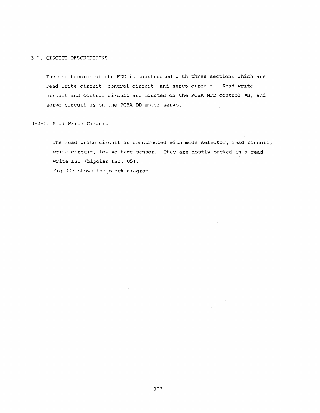
Page 14

w
a
CD
LOW
(Fig.303)
SIOEO
HEAD
~
'r----v--
t
'---.-'-----~
~---4~~
~~
--...r-
~
SI
ol-E
1----~:r-t---+-.--H--~:::=.!.--I~.19
HEAD
Block
read
RE
ADWRI H
ERASE
COMMON(CENTER
1,/9-12
2
~-I"'n-=--_
_ 8 L.::.:::.
,...
10 R"'11 r-:-=-
.....
J-=-..:;..--4---.
,..
9
"'lr
Crl3
..;
diagram
write
r.nll
COIL
r--
of
circuit
lAP)
R'iOO
__
-:.R~W...:..1..:..0
R"'01 -IT!f---+ MATRIX V
1r----~...:..:..-..l{I[
oY~~
HJ,.
.....~
~"
~--++---=C~OM~O~r--'
L
R12
_+----'\NvA\r-if-+-_~E:..!:::D~1
WT
'liT
COM
EVCC
GA
JN SELEClOR I
S4/55
I
'-----.·r-Cll---
~
rw
~;J
~
_
--fIool..ff3f---+
r-:-=- r
-L1l.
18
l..!.£..
1 r;-;::::-
~
ill
--1m
~
[It
HER
HE
AO
SW
ITCH
COMI.ION
DR
I Veil r J I
I 1
t,
ASE
DRJVEIl
....C)-----cn-J
~
~.~ ~ ~
r10l
nh
~
f--tl.
f--tl.
'---
I
WR
leu
SOURCE
TP4
A5V'"
A
/..).
'8~ '7~
PRE.
AMP
I
WRJTE
DRIVER
llE
R
RENT
PASS Fl:LTER
L4. L5. RA1L C1B.C29
I
TPS
...
C17
C20
:;
>0
:;
."
."
'6~
,h
I
~CT
0 JFFERE
=:E.
l~
/I
'iR J
TE
LOW
LV
'.
DV
EVCC
GG
t , t t t IfR0
~~4U~D6@~~~~;D~~@~~~~~
Rl1
---J.\IV'I..--+-t-
....
'--------.t
~\1SY),lMETRY
ft
~
ADJUSTOR
OV~EGND
1,/1-22
I
I
WRI1E
Re.
6
WRITE
DATA
...,
0
-.l
o
R9.Q1
-:
n n
VI
~
CURRENT
5WJTCH
~,
« n «
tn
I 0 I
VI
0
WG
_..--J
EG-....
....
I:;)
-------'
SWITCH
C30.C31.07.
I
OJ.FFERENTIATOR
R~2.
C32.
0 0 0
:;; :;; :;;
~.~ r9~
L3.
·0
"?1
'2~
J,
~
I
VE
NH
AT
OR
.'
VOLTAGE
sol
I ITIME
I
CONlR
lOG IC
c:
,..,
C)
~
SENSOR
LV
S1 tiil
~
I'-J"r
I
0L : 1
TPc I' IDRI
"'1"32
0_
SIDE
SELECT
r-
~l.J)
,-,
I-"
< LJ
III
I'
I
OUTPUT
I
1,/1
6
ONE
READ
DATA
FILTER 1
oa.
U1
I~-l-RA-C-K---SW---IT-C-H-.-SF-----------
I
C35
r0lLol
JL.:.F~
0
rn-~~.C
~E
ETECTOR
DOMAIN
I F I L
TER
~£r
DR
:llCI
----
VER
~-----
-30
~
~
'I-
~
AK
/ ..:uo....J
t'acP
~
~
~
~
tEJ
~
~
~14-=-:;;"'--+-
~
JVER
ill
DRIVE
SELECT
-..
:h
C25
~TPe
DIFO
......
I--...J
CJ
......
:....:...._--S-y-6---4Ib-
A
DVGG
lDeR
RDCR
DGND
LVGG
CD
OINV
os
.....
r---r----'--,.-I-..-'-...---..---,
:»-
'0
G>
=
lJ'J
:x
»
"
."
V)
G>
=
:x
qp
I r
......
.-
0
0
"'0
,..,
'<
z :x
"-
:10
0
-<
0
0
:=
"'0
,..,
Cj)
:x
z
"-
:10
0
-<
0
.....-
I
I
1
T
C24
-:
l'ME
C21. C22.
"tJ
::
n 0
CD
G>
,..
,
,.,.,
."
:=
n
(j')
CD
:x
."
.....
I
»
-0
V)
TRACK
SWI
TP7
---.
CONSTAllT
RAg
'0
0
c::
-l
"'0
c::
-l
n
0
z:
-l
:lC
0
,...
J
TCU
Page 15
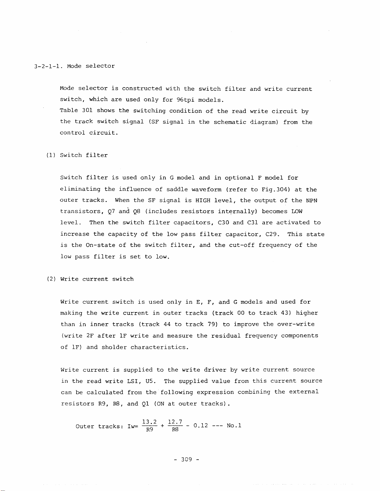
3-2-1-1.
Mode
Mode
selector
selector
is
constructed
with
the
switch
filter
and
write
current
(1)
switch,
Table
the
301
track
control
Switch
Switch
eliminating
outer
tracks.
transistors,
level.
increase
is
the
low
pass
which
shows
switch
circuit.
filter
filter
Then
the
On-state
filter
are
is
the
When
Q7
the
capacity
used
the
switching
signal
used
influence
the
and
Q8
switch
of
the
is
set
only
(SF
only
SF
(includes
filter
of
the
switch
to
in
of
signal
low.
for
condition
signal
G
saddle
capacitors,
low
filter,
96tpi
in
model
is
resistors
pass
models.
of
the
and
waveform
HIGH
filter
and
the
read
write
schematic
in
optional
(refer
level,
diagram)
to
the
int~rnally)
C30
and
C3l
capacitor,
the
cut-off
F
model
Fig.304)
output
becomes
are
C29.
frequency
circuit
from
for
at
of
the
LOW
activated
This
of
by
the
the
NPN
to
state
the
(2)
Write
Write
making
than
(write
of
IF)
Write
in
the
can
be
resistors
Outer
current
current
the
in
inner
2F
and
current
read
calculated
write
after
sholder
write
R9,
tracks:
switch
switch
current
tracks
IF
is
supplied
R8,
LSI,
from
and
Iw=
is
used
in
outer
(track
write
44
and
characteristics.
to
US.
The
the
following
Ql
(ON
13.2
~
+
only
to
measure
the
write
supplied
at
outer
12.7
~
in
E,
tracks
track
the
expression
-
O.
F,
(track
79)
residual
driver
value
tracks)
12
---
and
to
G
00
improve
by
from
combining
.
1
No.
models
to
frequency
write
this
and
track
the
current
used
43)
over-write
components
current
the
for
higher
source
source
external
-
309
-
Page 16
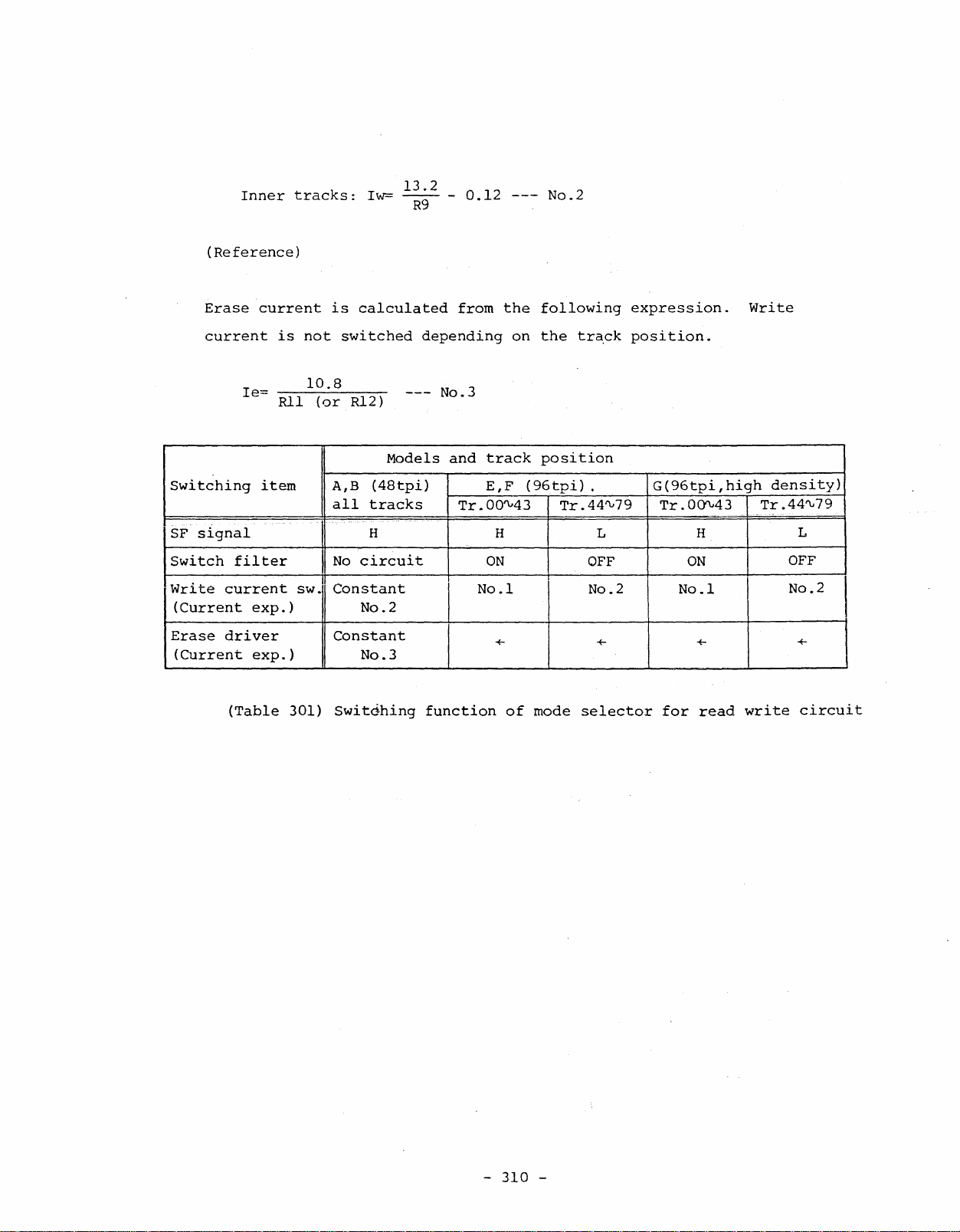
Inner
(Reference)
tracks:
Iw=
13.2
---R9
-
0.12
---
No.2
Erase
current
Switching
SF
signal
Switch
Write
current
(Current
Erase
driver
(Current
(Table
Ie=
filter
exp.)
exp.)
current
is
Rll
item
......
.
sw.
301)
not
10.8
(or
is
I
calculated
switched
R12)
---
Models
(48tpi)
A,B
all
tracks
.....
H H L H
No
circuit
Constant
from
depending
No.3
and
Tr.00'V43
No.1
the
track
E,F
ON
on
(96tpi)
following
the
tr~ck
position
.
Tr.44'V79
OFF
No.2
No.2
Constant
+
+
No.3
Switdhing
function
of
mode
selector
expression.
position.
G(96tpi,high
Tr.0Q'V43
ON
No.1
+
for
read
Write
density)
Tr.44'\.,79
OFF
write
L
No.2
+
circuit
-
310
-
Page 17
3-2-1-2.
The
low
Read
read
pass
circuit
circuit
filter,
consists
of
differentiation
head
matrix
amplifier,
switch,
peak
pre-amplifier,
detector,
time
domain
filter,
write
The
input
The
In
while
The
the
LSI,
minute
to
pre-amplifier
A~F
GSl-GSC
pre-amp.
low
frequency
position
same
time,
equalization.
the
differentiated
C24
and
The
time
and
output
US.
voltage
pre-amplifier
models,
is
output
pass
filter
noises.
of
the
further
C25
into
domain
driver.
induced
has
GSO-GSC
shorted
is
\
and
The
reproduced
amplifies
The
peak
output
a
~quare
filter
Main
in
read
via
matrix
three
is
in
gain
shorted
G
model
supplied
the
switch
differentiation
waveform
the
detector
after
wave.
eliminates
circuits
operation
switch
setting
to
to
to
the
filter
to
signal
constructed
passing
a
virtual
are
enclosed
by
for
selecting
terminals,
obtain
obtain
the
the
differentiation
to
~liminate
amplifier
zero
cross
with
the
with
through
pulse
the
read/write
GSa,
gain
gain
phase-shifts
point,
most
a
comparator
the
coupling
caused
in
the
side
0/1
GSI
of
100
of
200
amplifier
undesirable
and
appropriate
by
the
read
head
heads.
and
GSC.
times,
times.
via
the
peak
at
the
converts
capacitors,
saddle
i·s
high
in
the
for
G
with
two
single
driver
In
the
are
some
single
APS
signal)
depending
versions).
positive
function.
low
model)
edge
shot.
and
RD
gates.
shot
read
frequency
at
detectors,
Then
the
driver
m.v.,
is
on
PCB
Anyway,
pulses
outer
output
(3-state
To
control
input
issue
the
area
the
in
the
at
tracks.
delay
signal
driver.
TDCR
parallel.
numbers
FDD
read
(IF
output)
terminal
signal
is
operation.
area,
The
single
is
(A
so
-
time
output
of
from
These
~
set
311
62.5KHz
domain
shot,
from
the
for
the
0,
E,
that
-
for
read
read
pulse
control
control
or
the
Table
the
write
F
A~F
filter
data
FDD
width
signals
~)
RD
302
models,
is
latch,
through
LSI,
setting
circuit
and
PDD
terminal
shows
125KHz
constructed
and
the
US,
there
of
(OPEN/ROYO/
are
different
models
outputs
the
control
data
RD
delay
(PCBA
Page 18
PCB
issue
No.
Typical
PCBA
Version
RD
output
TDCR
orNV
control
DS
No
positive
terminal
(RD
output:
at:
pulse
LOW
outputs
level)
on
RD
A"'D
_.
E
F'V
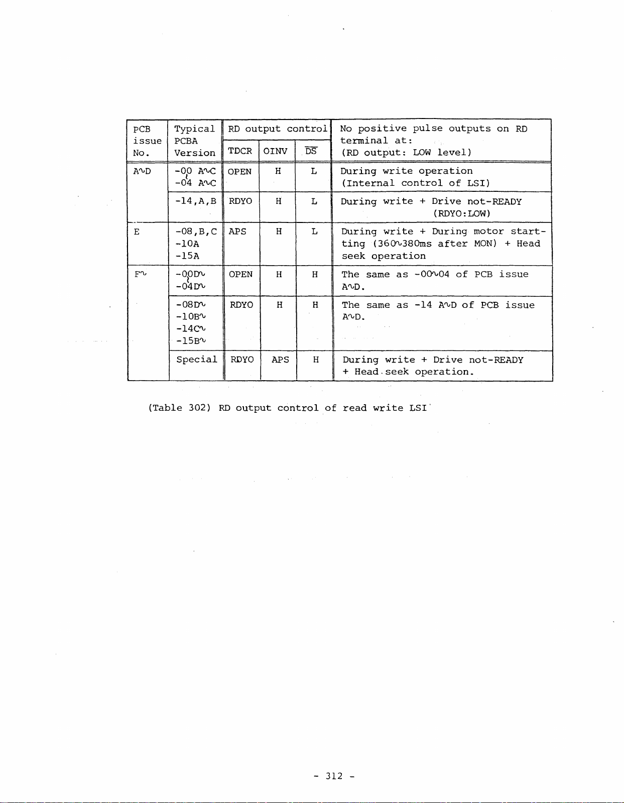
(Table
-00
A"-'C
(
-04
A"-'C
-14,A,B
-08,B,C
-lOA
-lSA
-OOD'\.
~
-040'\.
-080'\.
-lOB"-'
-14C'V
-ISH""
Special
302)
OPEN
RD
RDYO
APS
OPEN
RDYO
RDYO
output
H
H
H L
H
H
APS
control
During
L
(Internal
L
During
During
ting
seek
H
The
A"-'D.
H
The
A"-'D.
H
During
+
of
read
write
write
write
(36O'V380ms
operation
same
same
write
Head,
seek
write
control
-0Qt\..04
as
as
-14
operation.
LSI'
operation
of
Drive
+
(RDYO:LOW)
During
+
after
A"-'D
+
Drive
LSI)
not-READY
motor
MON)
of
PCB
PCB
of
not-READY
start-
+ Head
issue
issue
- 312 -
Page 19
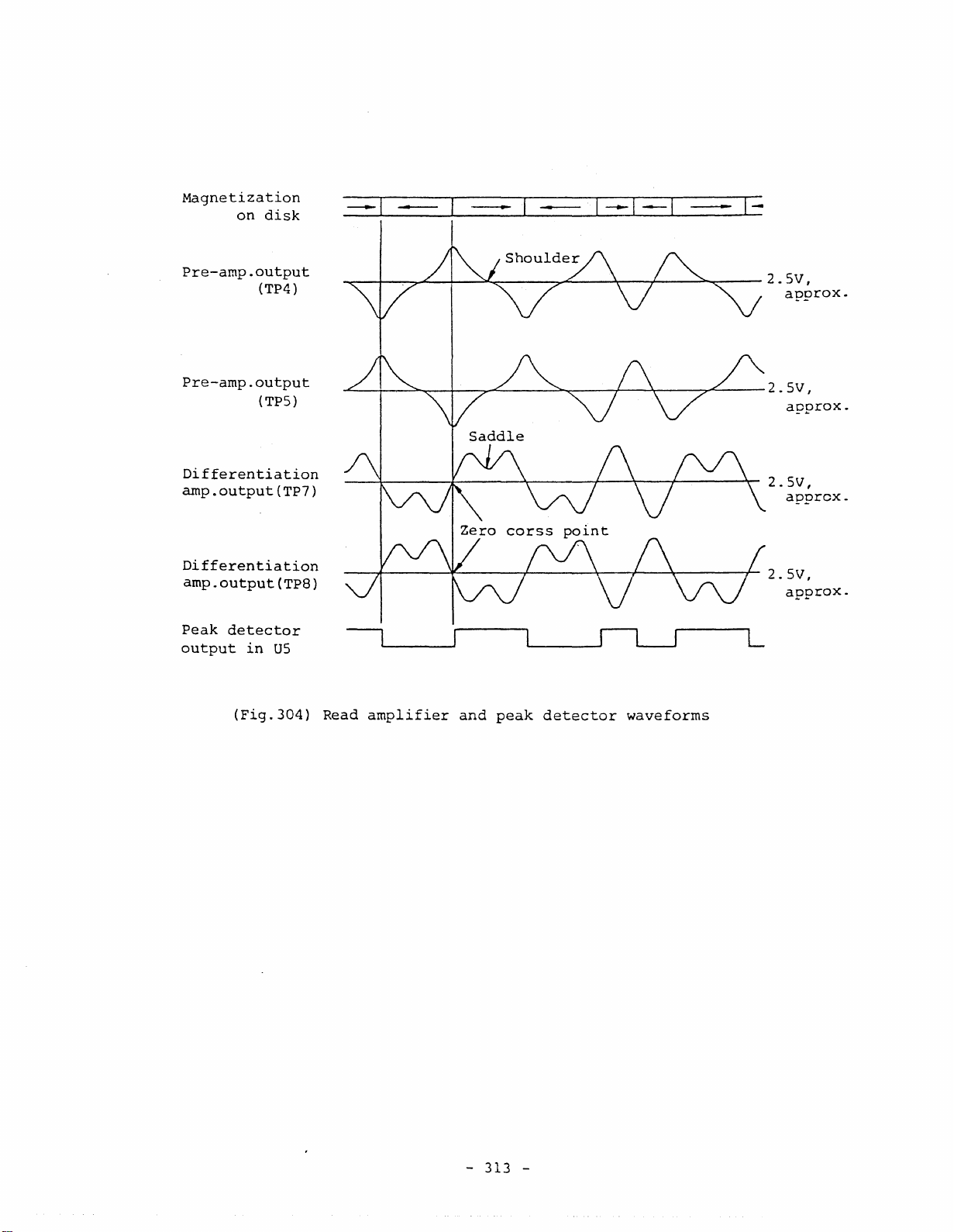
Magnetization
on
disk
Pre-amp.output
(TP4)
Pre-amp.output
(TP5)
Differentiation
amp.output(TP7)
Differentiation
amp.
Peak
output
output
detector
in
(TP8)
us
(Fig.304)
----l-~~-+--~:__----::;~---J't"-__t'---..;::".""r;::::.__-
2.
5V,
approx.
..L...--l-..:::::,.........--+--~::::..-----=::~---;f---'l~---::T'<::..---
2. 5V ,
approx.
2.5V,
approx.
--..l:..-----¥:----I---~r-----)'--_4:___--_t_
2.
5
V,
approx.
I~-
Read
amplifier
and
peak
detector
waveforms
L
- 313 -
Page 20

Peak
output
Edge
output
detector
in
detector
in
US
uS
#1
Virtual
pulse
(drop~in)
Delay
Q
output
Read
output
Edge
output
RD
output
READ
s.s.
in
data
latch
in
detector
in
DATA
(Fig.30S)
US
uS
#2
uS
(US-33)
(Jl-30)
I
T
I
-H--A"'F
U U
Time
domain
filter
n
models:
and
Ills,
read
n
U
approx.
gate
LJLJl
G
model:
,
LnJIJ
waveforms
fL
O.S\.ls,approx.
LJ
- 314 -
Page 21
3-2-1-3.
The
Write
write
circuit
circuit
consists
of
write
control
logic,
write
current
source,
write
circuits
Common
common
respectively.
SIDE
signals
COMl
cut
driver,
driver
terminals
ONE
is
off
Input
WG
Sl
H
H
I
H - L
L H
are
enclosed
SELECT
supplied
HIGH
in
the
signals
EG
H H
L
erase
output
The
level
read
-
H
(center
(Sl)
through
I
I
SIDE
SIDE
SIDE
SIDE
driver,
in
terminals,
outputs
input
(ll.sV,
write
FDD
0
0
0
1
common
the
read
taps)
of
signal,
the
write
approx.),
LSI
operation
read
operation
write
write
read
operation
driver,
write
COMO
of
the
the
common
to
inhibit
operation
operation
and
side
and
control
the
LSI,
COMl
driver
write
power
the
and
US.
are
0
and
gate
logic.
read
Output
COMO
2.7V
11.sV
11.SV
etc.
side
are
to
OV
connected
the
operation.
Most
1
heads,
controlled
(WG)/erase
When
voltage
the
read
of
the
to
gate
COMO
circuit
(approx.
COMl
2.7V
OV
OV
OV
the
by
or
the
(EG)
the
is
)
L
L
I
The
EG
changes
WG
signal
O.8srnm
read/write
signal
(tunnel
tracks
track
L
-
signal
to
-
L
HIGH
(refer
(A~F
gap,
so
that
erase).
preventing
(positioning
SIDE
SIDE
I
(Table
supplied
or
to
models)
it
the
The
deterioration
1
1
303)
from
LOW
level
Fig.306).
or
is
necessary
written
tunnel
error).
write
write
Common
the
O.s8srnm
data
erase
It
operation
operation
erase
with
Since
for
is
of
also
driver
timer
an
appropriate
the
(G
model)
the
completely
produces
the
ensures
erase
SiN
output
in
erase
backward
a
ratio
disk
OV
OV
the
control
time
gaps
locate
and
driver
trimmed
guard
band
resulting
interchangeability.
delay
to
by
11.SV
11.sV
circuit
against
about
across
delay
the
between
from
the
the
erase
the
a
the
WG
head
off-
-
315
-
Page 22
The
WRITE
DATA
input
pulse
is
latched
by
the
write
data
latch
in
the
write
current
the
WRITE
WG
(US-29)
EG
(TP2)
SIDE
,(Jl-J2)
WRITE
two
ONE
control
source
write
GATE
SELECT
DATA
logic.
drivers
(Jl-24)
(Jl-22)
is
And
supplied
alternately.
-
appropriate
to
the
Erase-on
delay
write
read/write
current
head
Erase-off
((
,
..
~\
(,~
by
delay
from
turning
the
___
write
on
and
off
L
L
Write
in
Write
(US-17,18,12tV1S)
Write
Magnetization
disk
uS
(Fig.J06)
data
driver
current
latch
output
on
Typical
waveform
of
write
circuit
Previous
operation
magnetization
-
J16
-
Page 23

3-2-1-4.
The
Low
voltage
low
voltage
sensor
sensor
is
equipped
to
protect
the
FDD
from
erroneous
operation
unstable
sensors
LVSO
monitors
of
the
it
supplies
write
driver,
protect
unstable
LVSl
is
circuit
of
3.SV
connected
the
LVS
LSI,
U3)
due
state
of
LVSO
read
the
state
equipped
in
item
through
to
signal
are
to
of
and
the
write
signals
erase
disk
of
3-2-2.
4.4V.
the
is
reset~
the
the
LVSl
+5V
LSI.
driver,
from
the
to
LVGG
LOW
internal
power
are
and
If
to
inhibit
an
erroneous
power
generate
As
The
terminal
level,
circuit
voltage
equipped
+12V
voltage
the
voltage
the
and
voltage.
LVS
well
monitored
all
write
signal
as
(pin
the
construction
such
as
in
supplied
is
operation
control
write
to
LVSO,
voltage
37)
of
control
at
the
lower
or
erroneous
be
it
the
power
read
of
logic
supplied
is
activated
by
read
circuits
write
to
than
the
the
of
the
on
the
3.SV
common
in
erase
LVSl
write
FDD
or
off.
LSI,
internal
through
driver,
the
LSI,
to
the
in
is
LSI.
(mainly
during
US.
during
control
the
only
control
Two
circuit
4.4V,
which
range
+5v
While
+sv
LVS
power
(US-32)
Power
(Fig.307)
on
Typical
3.S'\.4.4V
waveform
-
317
Power
of
low
voltage
-
off
-++--
sensor
3 .
5'\.4
. 4V
Page 24
3-2-1-5.
Function
and
operating
waveform
of
read
write
LSI
terminals
Following
operation
(1)
Pre-amplifier
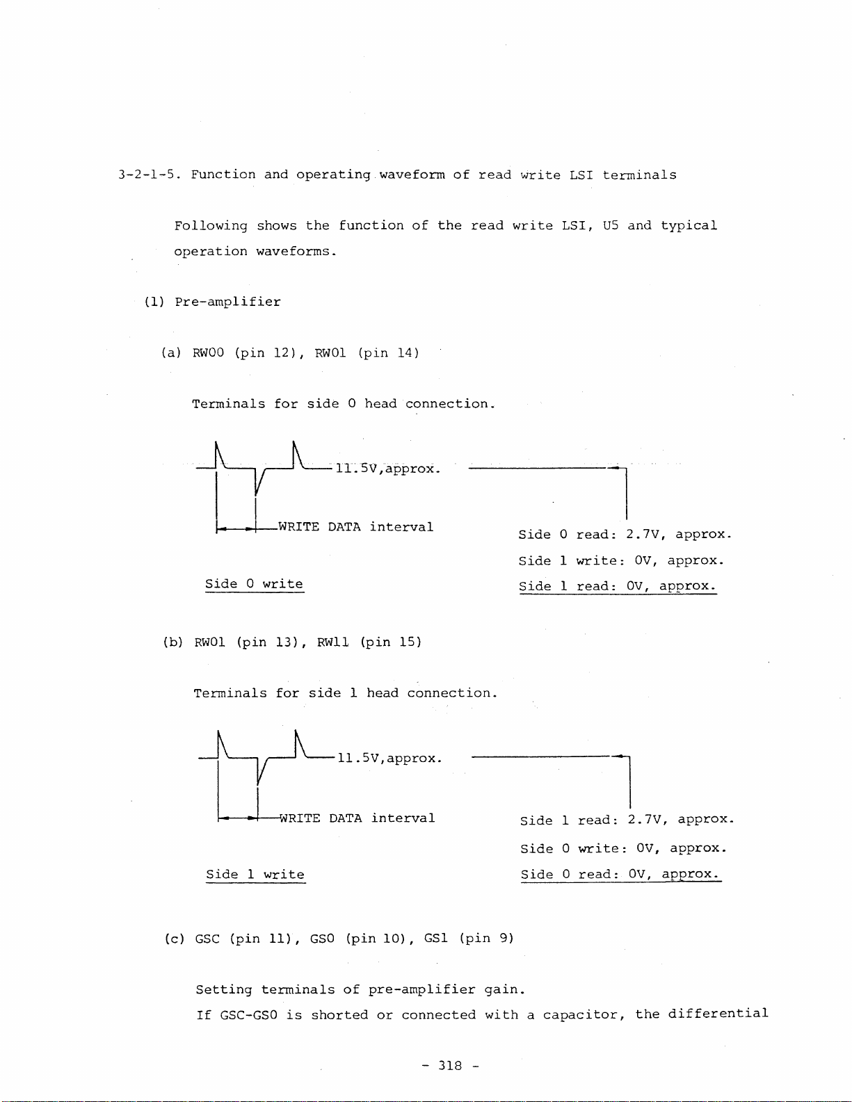
(a)
RWOO
Terminals
(pin
shows
waveforms.
12),
for
the
RWOl
side
function
(pin
0
head
of
the
read
14)
connection~
write
LSI,
US
and
~IL5v,approx.
I.
Side
-I
0
I
write
WRITE
DATA
interval
Side
Side
Side
0
1
1
read:
write:
read:
l
2.7V,
OV,
OV,
typical
approx.
approx.
approx.
(b)
(c)
RWOl
Terminals
(pin
Ll
Side
GSC
(pin
Setting
If
GSC-GSO
13),
for
1
write
II),
terminals
RITE
is
RWll
side
1
11.sV,approx.
DATA
GSO
(pin
of
shorted
(pin
15)
head
connection.
interval
10),
pre-amplifier
or
connected
GSl
(pin
9)
gain.
with
Side
Side
Side
a
capacitor,
1
0
0
read:
write:
read:
l
2.7V,
OV,
OV,
the
approx.
approx.
approx.
differential
-
318
-
Page 25
(d)
voltage
if
GSC-GSI
times.
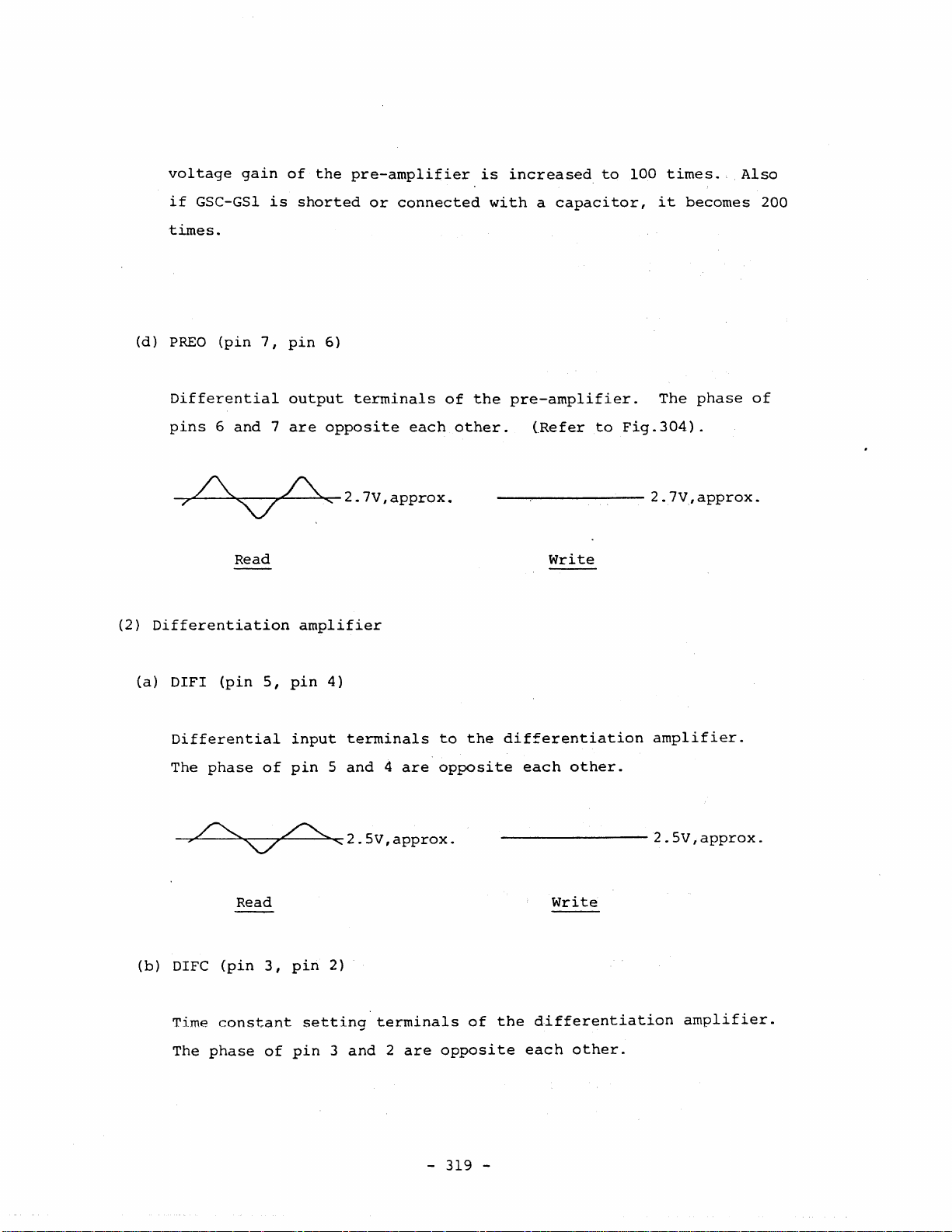
PREO
(pin
gain
7,
is
of
the
shorted
pin
pre-amplifier
or
6)
connected
is
with
increased
a
capacitor,
to
100
times.
it
becomes
Also
200
Differential
pins
-7....,.,L-~
(2)
Differentiation
(a)
DIFI
Differential
The
6
and7are
A
......
V----...e--~'-
Read
(pin
5,
phase
/"-.... •
» "'-7'
of
output
opposite
/\.
amplifier
pin
4)
input
pin5and
~
.....
terminals
2.
7V
,
appro
terminals
4
2.
SV,
approx.
each
are
of
the
other.
x •
to
the
opposite
pre-amplifier.
(Refer
---,-------
Write
differentiation
each
other.
---------
to
The
Fig.
304)
2.7V,approx.
amplifier.
2.Sv,approx.
phase
.
of
(b)
DIFC
Time
The
Read
(pin
constant
phase
3,
of
pin
setting
pin
2)
3
and2are
terminals
-
of
opposite
319
-
Write
the
differentiation
each
amplifier.
other.
Page 26

A A
---O/,.L----.oo...:V,.--r----..:>o.,',.-- 1 . 1
v,
a
pprox
.
---------
1.
lV,
approx,
(c)
(d)
Read
DIFO
Differential
The
CI
Differential
phase
(pin
phase
Read
(pin
of
43,
of
pin
1,
pin
output
pin
pin
input
43
44)
terminals
1
and
2.7V,approx.
42)
terminal
and
42
44
are
are
of
opposite
of
the
opposite
the
write
differentiation
each
write
comparator
each
other.
other.
(peak
amplifier.
2.7V,approx.
detector).
The
(3)
fV\
-j+---\W--+---\-\-
Time
domain
(a)
TDCR
Pulse
models
While
Read
(pin
width
use
this
fV\
filter
40)
setting
this
terminal
2 • 5
terminal
terminal
is
V,
approx.
forced
for
----------2.5V,approx.
write
of
the
delay
the
inhibit
to
be
LOW
-
320
-
single
gate
level,
of
the
shot
the
RD
delay
m.v.
pulse
single
Some
output.
shot
Page 27
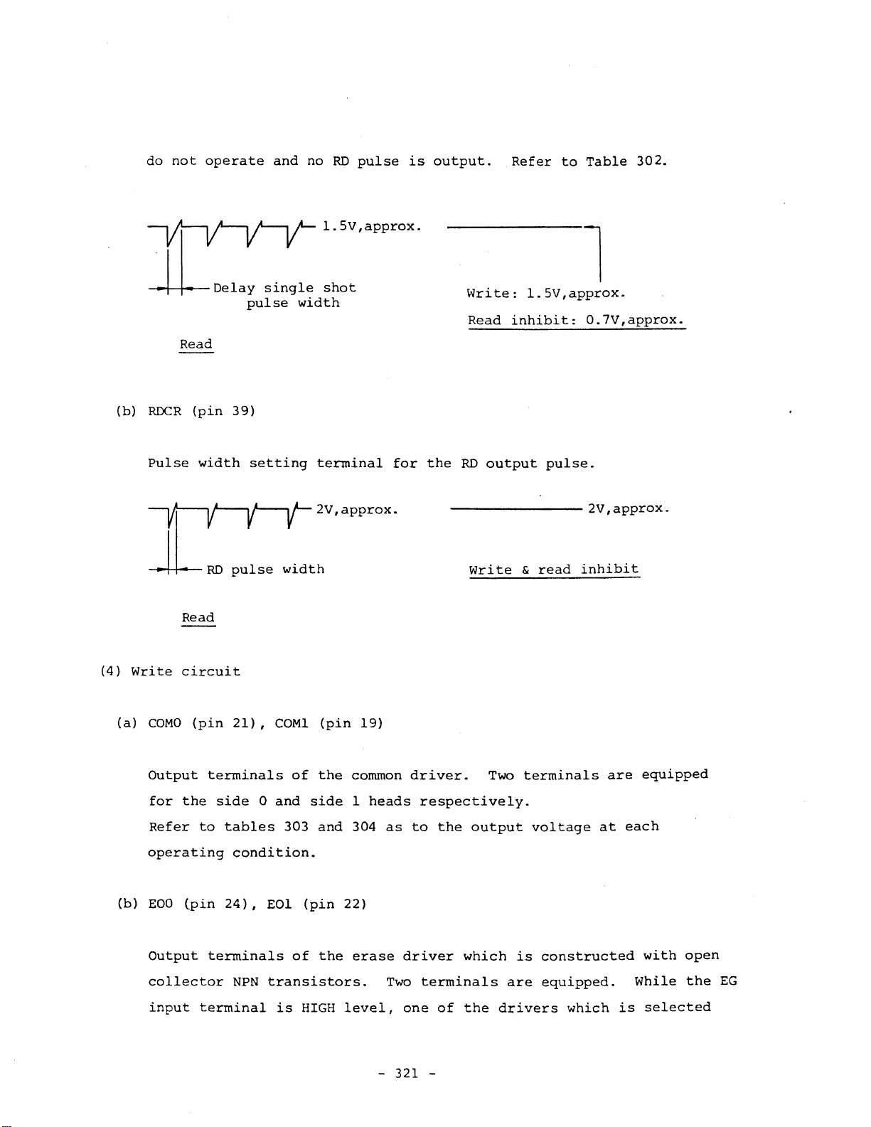
do
not
operate
and
no
RD
pulse
1.5V,approx.
is
output.
Refer
to
Table
302.
(4)
~
(b)
RDCR
Pulse
r-RD
Write
Read
(pin
width
Read
circuit
Delay
39)
pulse
single
pulse
setting
width
width
shot
terminal
2V,approx.
for
the
Write:
Read
RD
--------
write
inhibit:
output
l
1.5V,approx.
pulse.
&
read
inhibit
0.7V,approx.
2V,approx.
(a)
(b)
COMO
Output
for
Refer
operating
EOO
Output
collector
(pin
the
(pin
input
21),
terminals
side
to
tables
condition.
24),
terminals
NPN
terminal
COMl
of
0
and
303
EOl
(pin
of
transistors.
is
HIGH
(pin
the
side
and
the
19)
cornmon
1
heads
304
22)
erase
level,
-
as
Two
321
driver.
respectively.
to
the
driver
terminals
one
of
-
Two
output
which
the
terminals
is
are
drivers
voltage
constructed
equipped.
which
at
are
equipped
each
While
is
with
selected
open
the
EG
Page 28
by
the
CS
input
terminal
turns
on
(becomes
LOW).
(c)
Refer
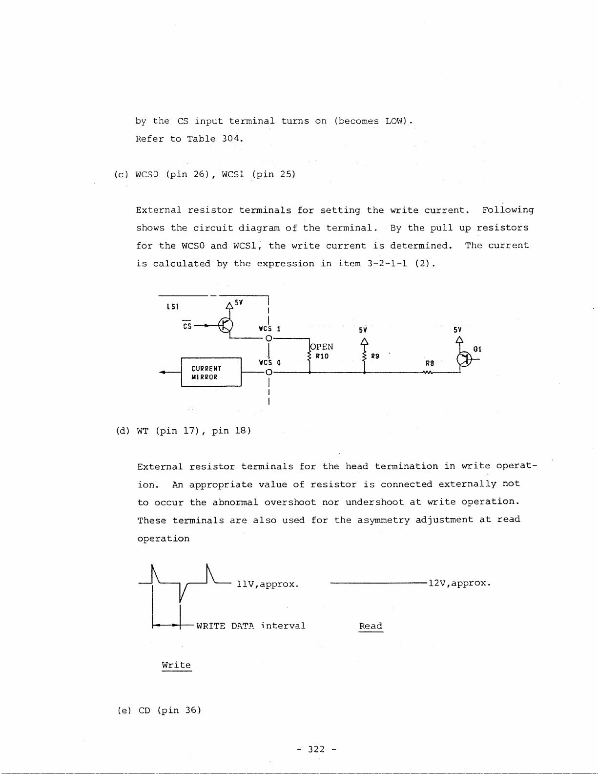
WCSO
External
shows
for
the
is
calculated
to
(pin
the
Table
26),
resistor
circuit
WCSO
and
by
304.
WCSI
WCSl,
the
(pin
terminals
diagram
the
expression
25)
of
for
the
write
setting
terminal.
current
in
item
the
write
By
is
determined.
3-2-1-1
the
(2).
current.
pull
up
The
Following
resistors
current
(d)
(e)
WT
(pin
17),
pin
18)
External
ion.
to
occur
These
operation
UWRITE
CD
(pin
An
terminals
Write
resistor
appropriate
the
abnormal
36)
terminals
are
llV,approx.
DATA
value
overshoot
also
interval
used
for
of
the
resistor
nor
for
the
---------12V
head
tennination
is
connected
undershoot
asymmetry
Read
externally
at
write
adjustment
in
write
operation.
,approx.
at
operat-
not
read
-
322
-
Page 29

In
order
to
protect
the
head
from
undersirable
magnetization,
this
(f)
terminal
at
a
determined
completion
WG
CD
CS
(pin
Control
Table
i)
304).
ON/OFF
is
used
to
set
the
direction
of
a
write
operation
H
~
1 $
27)
---
input
control
Schmitt
terminal
of
TTL
having
write
delay
for
input
current
time
1
through
(WG
I_L_
JL
following
setting
turns
to
keep
S~s,
off).
1.5V.approx.
Delay
two
the
approx.,
time
functions.
terminal
write
WCSl.
after
current
the
(Refer
flow
to
(5)
(g)
(h)
ii)
WD
WRITE
WG
Control
from
Others
Selection
(pin
28)
DATA
~vri
te
(pin
29),
input
the
of
---
input
control
erase
Schmitt
terminal
EG
(pin
terminals
circuit
driver
30)
TTL
---
for
in
input
from
write
the
output
the
Schmitt
FDD.
terminals
host
---------
TTL
permit
controller.
Read
input
(WG)
Refer
to
EOO
and
Tables
and
erase
E01.
SV,approx.
permit
304
and
(EG)
305.
-
323
-
Page 30
(a)
Sl
SIDE
The
(pin
ONE
terminal
31)
SELECT
---
Schmitt
input
functions
TTL
terminal
as
the
input
selector
from
the
for
host
controller.
common
driver
outputs
COMO/COMl
Refer
(b)
LVS
LVS
to
(e)
OINV
Control
(d)
AGND
OV
to
(pin
signal
item
(pin
(pin
power
and
Table
32)
output
3-2-1-4.
35),
input
16),
terminals
for
304.
---
DS
terminal
EGND
head
Open
terminal
(pin
mainly
switch
collector
34)
of
(pin
RD
23),
for
to
---
matrix
TTL
the
TTL
output.
and
the
of
output
control
input
Refer
DGND
following
RWOO,Ol/RW
circuit
to
Tables
(pin
38)
circuits
10,11
of
the
302
in
terminals.
FDD.
and
the
LSI.
Refer
(e)
(f)
AGND:
EGND:
DGND:
AVGG
+5v
AVGG:
AVGG:
LVGG:
EVCC
+12V
Analog
Erase
Digital
(pin
power
Analog
Digital
Low
(pin
power
operation
driver.
operation
8),
DVGG
terminals
operation
operation
voltage
20)
terminal.
(pin
mainly
sensor
circuits
circuits
41),
circuits
circuits
(LVSl).
for
-
LVGG
the
324
such
such
(pin
such
such
-
as
pre-amplifier.
as
37)
following
as
pre-amplifier.
as
write
write
control
circuits
control
logic.
in
logic.
the
LSI.
Page 31

R
e
a·
d
WG
L L
L L
L
L L
EG
L
Inputs
-
Sl
H
L
-
H
- -
CS
-
-
-
-
OS
Outputs
OINV
L
L
H
-
--
LVS
COMO
L H
L H
L H
H H R
EOO
COMl
R
0
0
R Z Z
0 Z Z
EOl
Z Z N 0
Z Z
Write
I
RD
current
N
Z 0
!
P
0
0
L L
W
r
/
E
r
a
e
LV
L:
H
i
t
e
s
Logic
L H
L H
H H
H
L
L H
H H
H
L H
L H H L -
H H H
H
L
L H L
H H
-
- -
level
L
H H
H
L
L
L
L
L L
(LOW)
0
-
H
-
-
- -
H
H
H -
H
L
L -
L - -
L
- - H
-
-
-
-
-
-
-
H H
-
-
-
-
-
I
-
-
-
-
-
R:
0
H
Hi
H
Hi
Hi
H
H
L
COM
0
0
0
Hi
Hi
Hi
0
0
0
voltage,
Hi
Hi
Hi
Hi
Hi
Hi
H
H
H F
H
H
H
H 0
R
0 z
0
0
0
0 Z
0 z
0
2.7V,
Z Z
0
0
Z Z
0 Z
0
Z
Z
Z
Z
Z
z
Z
Z
Z 0
Z
0
0
Z F
0
0
Z Z
approx.
P
F
WCS
F
F
F
F
WCS
WCS
F 0
WCS
WCS
F 0
F
WCS
WCS
F
WCS
F
0
0
0
0
0
0+1
0+1
0+1
0
0+1
0
H:
z:
Hi:
Logic
High
COM
level
impedance
voltage,
(Table
1 (HIGH)
(OPEN)
ll.5V,
304)
approx.
Read
write
-
P:
N:
F:
LV:
LSI
325
positive
Negative
FALSE (No
Low
voltage
control
-
pulse
pulse
pulse
table
output)
Page 32

3-2-2.
Control
The
control
Circuit
circuit
consists
of
strap
circuit,
LED&head
load
control
circuit,
stepping
interface
Almost
LSI,
U3.
(less
the
input
Fig.308
write/erase
motor
driver,
all
Since
than
terminal.
shows
control
the
circuits
the
±l~A)
the
control
circuit,
circuit,
etc.
except
LSI
is
a
CMOS
andaprotective
block
diagram.
track
for
motor
counter,
drivers
type,
register
input
on
are
is
gate,
disk
enclosed
current
serially
ready
change
is
inserted
detector,
circuit,
in
the
very
control
small
in
-
326
-
Page 33

W
10
~.J
(Fig.308)
STEP
WRllE
MOTOR
INDElC
TRACK
WRllE
PROTECT
READYI
DISK
GAlE
ON
00
CHANGE
Block
of
diagram
control
STRAPS
RY.
Xl
circuit
/r-----------:.~-~:.......::...:....;,:...::...:...:.....:-------__.\.
TO/FRO~
ROYO
l.40N1
l.40NO
READ
VRITE
APS
CIRCUIT
VG
EGLVS
SF
DSEl
~
I
ISTP
ill
DeDO
IDXO
TOO
WPO
RDYO
CLOCK
~--+-J
LSI
U3
I 1
CLOCK
GENERATOR
---.
I
~.
LEW
I
ov+
FRONT
INDEX
SENSOR
LED
STEPP
MOTOR
I
NG
L :
A.S
H E'G
MODEL(4BtDI)_
MODEl(96tcl)
~
L :
A'F
H G
MODELC300rorn)
MODEl(360rorn)
L..-.._--=":...:'_-.=,3
..
~C
FOR
0n
SPINDLE
MOTO~
Page 34

3-2-2-1.
In
Strap
order
circuit
to
select
the
various
function
by
users,
various
strap
posts
as
Some
wires
to
.to
the
are
the
models
instead
version
available.
details
have
of
table
not
the
of
Refer
strap
strap
strap
in
the
to
the
function.
posts.
posts,
schematic
Specification
These
and
models
~~e
diagraml.
function
items
have
soldered
is
1-11
fixed.
and
jumping
(Refer
1-12
-
328
-
Page 35

3-2-2-2.
The
LED
circuits
and
head
load
consists
control
of
circuit
LED/Head
load
gate,
overdrive
timer
1,
LED
driver,
(1) LED/Head
To
the
and
IN
According
signal)
to
the
(a)
DLED
A
signal
While
Strap
Ul
OFF
OFF
ON
solenoid
load
LED/Head
USE
(IU}/HEAD
to
the
and
U2
LED
driver
signal
to
this
signal
setting
U2
OFF
ON
OFF
gate
(US2
turn
driver,
load
selected
and
on
U3
USI
L
L
H
gate
LOAD
signal),
the
the
is
LOW
input
US2
and
in
(IHL)
function
solenoid
front
level,
L
H
L
overdrive
the
control
signals
these
bezel
the
LED
on
(No
~elation
-
(L)
IU
-
(L)
IU
(L)
IU
circuit
LSI,
are
designated
input
driver
signals
indicator
LED
condition
--
+
OSEL
--
+
OSEL
input.
as
turns
to
1.
U3,
by
OLEO
HL
(L)
(L)
DRIVE
the
are
and
(LED).
on.
(OLEO
strap
SELECT
straps
gated
HLC
LOW)
& IHL
Ul (USI
to
output
signals.
input)
(DSEL)
(b)
ON
HLC
signal
A
signal
solenoid.
ON
RDYO:
(Table
to
U3,
activate
While
H
Ready
305)
this
H
detector
LED
the
signal
IU
turn-on
solenoid
is
-
(L)
output
LOW
329
+
DSEL
signal.
condition
for
the
level,
-
(L) x
models
the
ROY
a
HIGH
with
solenoid
(H)
in
ready.
head
is
load
activated.
Page 36

Strap
Ul
setting
U2
BL
USl
U3
input
US2
--
IHL
Solenoid
(No
relation
on
condition
to
IU
(HLS HIGH)
strap
&
IU
input)
(2)
OFF OFF OFF
OFF OFF
OFF
ON
OFF
ON
ON
OFF
ON
OFF
ON
ON
ON
ON
Note:
LED
driver
ON
OFF L
ON
OFF
ON
OFF B
ON
PRDY=
Pre-ready:
RDYO
(Table
L
L L
L
H L
H
H
(see
Internal
one
306)
L
L/H
H
H
L/H
L
LIB
H
H
LIB
Table
rotation
Solenoid
L DSEL
DSEL
PRDY
L
--
IHL
The
L
The
L
The
The
305)
signal
of
drive
(L)
(L)
---
(L)
same
same
same
same
+
Pre-ready
of
LSI.
the
condition
x
disk
x
PRDY
x
IHL
No.3
PRDY
as
as
as
as
No.1
No.2
No.1
No.2
It
(one
---
(L)
x
No.4
---
becomes
INDEX
No.1
PRDY
---
TRUE
pulse)
No.2
before
DLED
driver
collector
(3)
Solenoid
The
lKQ
construction
(4)
Overdrive
The
LSI.
For
output
signal
HLC
is
HLC
The
the
IC,
U7.
output).
driver
signal
supplied
timer
signal
overdrive
initial
(open
from
of
drain)
the
U7
from
to
U7.
1
is
also
26msec
control
is
constructed
Refer
the
the
driver
supplied
timer
of
LOW
to
control
is
the
level.
LSI,
U3
with
Fig.309.
LSI,
IC,
U7.
to
the
constructed
solenoid
is
inverted
NPN
U3
with
Refer
overdrive
activation,
transistor
with
and
a
pull
to
Fig.309
timer
a
retriggerable
is
up
it
input
array
resistor
as
to
in
the
maintains
to
(open
the
control
counter.
of
the
the
HOD
-
330
-
Page 37

vee
-1
.....
1-...-0
CQA
IN
STB
- - --M-- -
STa
IN
IN
IN
1N
IN
JN
GNO
(Fig.309)
+---
1
3
4
5
6
Construction
20K
......-.......
of
-~-
OUT
driver
.......
1
2
3
4
5
6
--n
IC,
OUT
GHO
U7
(5)
Overdrive
The
overdrive
level.
the
After
+5v
In
some
emitter-collector
the
circuit
HOD
signal
circuit
+l2V
drawing-in
the
overdrive
power
through
models,
solenoid.
is
power
action
1
input
1
and
is
period,
the
overdrive
of
Q5.
to
it
applied
of
the
diode
the
PNP
makes
to
solenoid
the
CRl
function
In
such
-
transistor
Q5
turn
the
solenoid
to
save
is
a
model,
331
-
on
solenoid
securely.
maintains
the
not
Q5
while
at
power.
equipped
+l2V
which
the
that
is
signal
time
its
with
always
constructs
to
situation
shorting
supplied
is
LOW
execute
the
with
the
to
Page 38

HLC
input
HOD
output
Applied
to
solenoid
voltage
coil
(Fig.310)
l
--_,-llv,approx.
J
I I
~overdrive
approx.
Overdrive
1~---------------12V'
I
,
~----OV
period
timing
of
head
load
solenoid
approx.
4V,approx.
- 332 -
Page 39

3-2-2-3.
Write/erase
The
circuit
control
consists
circuit
of
write/erase
gate
and
erase
timer.
Most
of
the
(1)
(a)
(b)
parts
of
Write/erase
The
gate
If
it
can
LSI
and
The
WG
are
different
Control
WG=
DSEL(L) x IWG(L) x
Control
--
WG=
DSEL(L} x IWG(L) x
the
judges
be,
erase
signal
LSI
LSI:
circuit
gate
whether
the
timer.
becomes
depending
No.:
2206-00
--
are
circuit
2206-00
enclosed
new
supplies
TRUE
on
FPT(L)
LHS060B
FPT(L)
data
in
the
each
LHS060
in
the
can
be
written
the
WG
followin~
LSI
No.
or
LHS060A
x
MON
delay
control
signal
condition.
1 x SEEK
on
LSI,
for
an
U3.
installed
the
read
The
disk.
write
conditions
(2)
Notes
Erase
WG:
Write
operation
DSEL: DRIVE SELECT
IWG: WRITE
FPT:
File
The
enable
is
MaN
delay
GATE
protect
same
notch
equivalent
1:
Internal
motor-on
SEEK:
Internal
operation
48tpi
~fter
timer
at
input
input
sensor
as
that
(light
to
command.
signal
(not
the
HIGH
signal
the
that
signal
of
in
last
signal
output
passing
Refer
LSI.
10
file
the
of
~
12msec
<::'!-o...--
---1:'
LOW.
LOW.
protect
WPO
LSI.
to
The
...--,,1<::0\
J:""--~-'
(FPT
input
condition)
output
360
Fig.31l.
ehad
for
•
sensor
of
~
is
not
96tpi
of
LSI)
detects
of
a
LSI
380msec
under
and
LOW.
the
disk
is
HIGH.
after
which
a
seek
13~l5msec
write
for
-
333
-
Page 40

The
circuit
to
make
the
WG
signal
delay
from
the
write/erase
gate
as
in
Fig.306
3-2-1-3.
Various
the
control
FDD
here.
FDD
A'\rF
(300rpm)
G
model
(360rpm)
Note:
to
delay
model
model
output
time
LSI.
ERO
H L L L
H
The
figure
excluding
(Table
the
Only
U3
307)
can
input
ERI
L
in
the
EG
signal
be
the
terminals
the
tolerance
Erase
set
SPED
ER2
L
above
delay
for
by
ERO~ER3
terminal
SPED
H
table
of
control
the
read
and
is
used
Erase
On-delay
250~26711s
19l1\,200lis
is
the
the
oscillator.
table
write
LSI.
SPED
for
delay
Off-delay
883~90011s
54l~550lJs
calculated
input
selection
Refer
terminals
value
to
of
item
of
the
- 334 -
Page 41

3-2-2-4.
The
Motor
circuit,
on
gate
receiving
a
spindle
motor-on
command
from
the
host
controller,
servo
and
A
123us
The
and
The
circuit.
auto-turn
motor-on
delay
delay
protects
MC
circuit
signal
supply
The
circuit
command
circuit
the
becomes
the
circuit
which
input
via
eliminates
control
TRUE
MC=(MONO(L) + MONl(L» x
Notes
MC:
MONO:
MONl:
Motor
MOTOR
Differs
Issue
Issue
rotation
ON
depending
A~E:
F
~
MC
the
input
(motor
consists
are
to
the
OR-gate
circuit
in
123us
at
Fixed
DLED
enclosed
MONO
the
the
delay
HIGH
signal
on
control)
of
or
to
noises
from
erroneous
following
x
LOW
PCB
at
FALSE (HIGH)
is
low
signal
OR-gate,
in
MONI
be
delayed
mixed
DISK
issue.
at
ML
to
123us
the
control
terminal
for
onto
operation.
conditions.
strap
the
spindle
delay
LSI,
lS
supplied
123~267us.
the
interface
is
ON.
motor
circuit
U3.
to
line
DISK:
The
auto-turn
a
disk
by
protect
than
state
mai~tai~s
insertion
the
information
sensor,
10
seconds
byacommand
Normally
For
a
circuit
~ALSE
optional
disk
to
and
after
(LOW
is
makes
improve
of
a
is
the
from
level)
fixed
inserted.
disk
reset
insertion.
this
(Front
to
FDDs
the
the
insertion
at
circuit,
.
bezel
TRUE
with
spindle
chucking
the
detection
indicator
(HIGH).
disk
motor
from
Even
the
sensor,
rotates
accuracy.
the
of
though
RDYO
is
disk
a
signal
ON).
it
becomes
automatically
The
sensor
ready
the
FDD
in
circuit
state
becomes
item
HIGH
and
when
is
file
or
more
3-2-2-5
at
set
ready
335
-
-
Page 42

3-2-2-5.
Ready
detector
Ready'
pre-ready
the
LSI,
block
The
Me
detector
As
the
then
pre-ready
twice
speed
pulse
condition.
are
detected
speed
detected
detect6r
latch,
U3.
of
ready
signal
which
motor
of
the
detector
interval
reaches
after
consists
In
detector.
for
enables
speed
latch
nominal
starts
at
The
after
within
the
ready
the
controlling
increases,
the
ready
the
pre-ready
of
latch,
block
the
is
set
condition
its
operation
IDXS
latch
motor
±6%
of
50%
speed
MON
diagram,
the
operation
50%
when
(i.e.,
terminal
is
set
start.
the
state.
delay
spindle
speed
the
rated
detector,
these
of
pulse
50%
and
becomes
when
In
speed
The
circuit
circuits
motor
all
the
detector
interval
of
sets
within
more
the
typical
when
ready
disk
the
than
±6%
which
is
above
operates
ready
the
latch
speed
are
are
input
becomes
speed).
±6%
three
case,
next
will
shown
five
latch
of
index
detector,
enclosed
as
to
the
circuits.
first,
less
Then
when
the
the
pulse
be
set
in
one
ready
and
than
±6%
the
nominal
pulses
motor
is
at
that
time.
Operation
signal
for
360rpm
On
the
after
signal
the
other
delay
are
output
the
FDD
ready
modes
and
other
the
MC
to
be
is
2
signal
is
detector.
the
(A~F
hand,
signal
supplied
the
from
read/write
RDYO=MCx±6%
Notes
RDYO:
of
index
MON
and
the
The
speed
Ready
the
pulse
models)
the
becomes
to
delay
the
control
RDYO
at
two
or
MON
write/erase
ready
ready
x
MON
HIGH
speed
interval
300rpm
delay
TRUE.
2
signal
latch
LSI
state.
signal
delay
detectors
will
(G
circuit
One
output
as
the
Fig.3ll
goes
2
gate
(380
TRUE
be
model)
generates
of
them
(360
~
coinciding
RDYO
are
changed
detected
.
is
~
400msec
signal
shows
in
the
appropriately
two
the
MON
380msec
delay).
through
which
the
following
by
delay
delay)
indicates
timing
the
SPED
signals
delay
The
AND
chart
conditions.
1
and
MON
gate
that
of
-
336
-
Page 43

MC
(Motor
on
command)
MC:
±6%
MON
MC
signal
speed:
delay
--I
to
IDXS
pulse
2:
380~400ms
the
spindle
interval
after
motor
is
MC
HIGH
within
signal
(motor
±6%
becomes
rotates).
of
nominal
HIGH.
value.
Disk
rotation
IOXS
(TPl)
(Index
50%
speed
in
U3
Pre-ready
in
U3
Ready
MON
delay
MON
delay
detection)
detection
latch
latch
1
2
in
in
in
speed
U3
U3
U3
400ms
36O'V380m
380~40Oms
Max.
...-----
2t
360rpm:
300rpm:
Max.
.....
Constant
l66.7ms
200ms
t±6%
speed
t
I~.~~--~
Pre-ready
RDYO
IOXO
output
output
Note:
Motor
300rpm:
(Fig.3ll)
360rpm:
300rpm:
on
A~F
Ready
models,
detector
73Oms,
800ms
360rpm:
-
337
Max.
Max.
G
waveforms
-
model
I
t7:ith
Head
load
solenoid
Ready
enable
model)
Page 44

All
the
five
parts
of
ready
detector
are
reset
by
the
Me
signal
going
FALSE
(LOW
level)
.
-
338
-
Page 45

3-2-2-6.
Stepping
motor
control
circuit
(I)
Stepping
step
generator,
coil
driver,
All
the
are
enclosed
enclosed
shown
Direction
At
every
direction
by
the
to
the
of
the
motor
control
shift
and
overdrive
above
as
circuit
one
circuits
in
the
block
in
of
latch
input
latch
of
the
samples
DIRECTION SELECT
bi-directional
stepping
motor
circuit
register,
except
control
the
the
STEP
shift
coil
circuit.
control
stepper
(ISTP)
and
(IDIR)
as
consists
phase
for
LSI,
LSI
holds
signal.
register
shown
the
U3.
except
control
pulse
the
drive
coil
In
head
and
in
of
direction
selector,
driver
the
for
circuit.
from
seek
The
changes
Fig.312.
block
the
the
'direction
latched
latch,
and
diagram,
overdrive
host
output
the
activating
internal
overdrive
overdrive
all
controller,
designated
is
timer,
circuit
the
timer
supplied
order
are
the
(2)
Internal
The
(a)
(b)
circuit
The
the
the
TRK
for
'When
space
motor
When
and
step
circuit
STEP
signal
is
HIGH
one
the
in
rotates
the
the
generator
has
generates
(ISTP)
level
step),
TRK
response
RE
strap
control
following
input
(96tpi
it
is
HIGH
for
LSI
at
purposes.
an
internal
pulse.
the
TRK
mode
or
is
not
executed.
level,
to
one
STEP
two
step
for
auto-recalibration
No.
is
This
terminal
48tpi
the
pulse.
space
2206-00
step
function
is
mode
stepping
(3.6°)
LHS060A
pulse
LOW
with
When
in
a
motor
it
response
is
or
3msec
is
executed
(48tpi
stepping
rotates
is
ON
(PCB
5060B,
approx.
mode).
LOW
motor
level,
to
issue
step
only
for
one
later
when
When
of
one
the
STEP
F
and
pulses
from
the
3.6°
step
stepping
pulse.
later)
for
-
339
-
Page 46

auto-recalibration
The
auto-recalibration
are
generated
starts
when
at
every
the
FDD
3msec
is
approx.
1
powered
on
and
the
LVS
(3)
signal
continues
The
maximum
During
NOT-ready
from
Shift
Step
shift
register
pulse
register
appropriate
4-phase
the
control
In
order
2-phase
from
the
the
stepping
to
drive
the
until
time
execution
state
host
and
timing
LSI
improve
period
read
the
required
(RDYO
controller
and
phase
the
output
and
the
signals
motor.
and
write
detection
of
output
drive
phase
supplied
the
torque
is
provided
LSI
of
for
auto-recalibration
the
auto-recalibration,
LOW)
is
ignored.
selector
of
the
drive
for
the
These
to
phase
the
margin
is
changed
the
and
direction
selector
uni-polar
drive
coil
by
the
track
in
the
driver.
the
phase
from
00.
STEP
latch
to
1-2
signals
seek
drive
LOW
(ISTP)
are
be
phase
to
is
255msec.
the
FDD
supplied
converted
drive
are
output
operation,
selector
HIGH,
maintains
pulse
and
input
to
to
of
from
partial
only
the
the
the
in
(4)
(5)
the
for
Coil
Four
the
as
Overdrive
External
SOD
initial
timing
driver
outputs,
coil
to
the
timer
2
retriggerable
output
Fig.313.
stage
chart.
PA,
driver
construction
timer
and
internal
in
the
(open
when
PB,
which
2
LSI.
counter.
drain)
the
PNA,
consists
of
step
The
During
from
drive
PNB
U7.
pulses
overdrive
the
phase
from
of
a
are
on-state
LSI
the
driver
timer
becomes
is
also
changed.
control
Ie,
supplied
2
is
of
the
LSI,
U7.
constructed
timer
LOW
level.
Refer
U3
Refer
to
the
(5Omsec;
to
are
to
with
Refer
Fig.312
input
Fig.309
overdrive
a
approx.)
to
to
i
-
340
-
Page 47

DIRECTION SELECT
(Jl-18,IDIR)
Step-out
Step-in
STEP
Direction
96tpi
(Jl-20,ISTP)
Internal
SOD
output
Coil
latch
(or
48tpi,3.6°):
(Overdrive
driver
PA
PB
PNA
PNB
step
in
gen.
timer
input
U3
in
2)
--IJ
__
U3
_
~_-....L
L..--.+-+-----+------::.-----+-----i
tl
__
....L-
Overdrive
..L..-_-L.
operatlon
t2
__
i50ms
.a~rox.
. I s--J
.
48tP:~ternal
SOD
(Overdrive
output
Coil
driver
PA
PB
PNB
PNB
step
tl:
t2:
gen.
timer
input
Internal
Partial
(Fig.3l2)
in
U3_~~-_·~+~--~~-~+-~a~~-I~~-~~(-~-;-s-:-~-~-~~r-o~x-)~~~_I~Oms::jprox.
2)
14----+----+--+-----+--+----<r-I
step
2-phase
Stepping
delay
activating
motor
tl
(3msec,
"\'
. .
1
control
t2
approx.)
period
circuit
tl
(O.6ms,approx.)
waveform
.11_
t2
-
341
-
Page 48

Final
in
U3
internal
step
pulse
n
---J
1 _
(6)
SOD
output
Applied
coils
Overdrive
The
SOD
overdrive
time
+12V
the
seek
After
voltage
signal
and
the
to
(Fig.313)
circuit
is
circuit
power
completion
is
settling
motor
2
input
2
and
applied
T-'----
..
I I
---.J
1
Stepping
to
the
it
makes
to
operations
of
the
settling,
__
------
sOms,
Overdrive
PNP
the
approx.
motor
transistor
Q6
turn
stepping
securely
period
overdrive
on
with
only
during
motor
+SV
llV,approx.
.---
-----
t
..1
timing
Q6"
which
coils
high
power
LOW
torque.
is
constructs
level.
to
execute
supplied
12V,approx.
4V,approx.
OV
the
At
that
to
the
coils
only
design,
consumption
through
the
required
heat
the
radiation
of
the
diode,
torque
stepping
CR3
for
is
which
holding
decreased
motor
minimize
the
to
in
seek
the
the
stop
minimum
stop
power
position.
is
only
level
loss
By
and
O.2SW,
by
the
the
supplying
above
power
approx.
-
34~
;,;.
Page 49

3-2-2-7.
Track
counter
Track
counter
signal
signal
control
models.
The
output
terminal
in
the
conditions.
TOO=
TOSxStep
Notes
for
to
LSI,
track
TOO:
TOS:
Step
the
the
Refer
signal
of
memorizes
read
host
U3.
to
the
LSI
counter.
out
Track
Track
Track
head
out:
direction.
write
controller.
The
function
item
3-2-1-1.
from
the
and
The
x
PA
00
detected
00
sensor
00
sensor
carriage
Direction
the
is
track
circuit.
track
output
TOO
output
detects
(track
latch
position
All
of
00
signal
at
It
the
this
sensor
as
HIGH.
at
00
output
also
circuits
circuit
the
TOO
becomes
TP3 (TOS
the
light
position)
in
and
outputs
(TP3)is
signal
TRUE
item
outputs
TOO
are
is
used
in
input
disturbing
.
3-2-2-6
track
(TRACK
enclosed
only
supplied
through
the
of
switch
in
in
to
the
following
LSI)
wing
is
step-out
00)
96tpi
is
of
(SP)
the
TOS
gate
HIGH.
the
When
the
constructed
is
executed,
44th
track.
Track
Track
PA:
PA
TOO
from
00~43:
44~79:
output
Phase
signal
the
Refer
A
coil
becomes
up-down
counter
to
SF
signal
SF
signal
from
item
stepping
of
the
TRUE
counters
steps
3-2-1-1
HIGH.
LOW.
up
motor
(HIGH
are
and
as
motor
reset.
the
to
control
is
activated.
level),
the
SF
the
If
a
output
function
circuit
track
step-in
changes
of
is
HIGH.
counters
operation
to
the
SF
LOW
signal.
at
~
343
~
Page 50

3-2-2-8.
Other
terminals
and
function
of
control
LSI
(1)
(2)
Following
APS
output
APS
signal
The
signal
models.
APS=
MON
Notes
OSCI,
MON
SEEK:
OSCO
explains
terminal
becomes
is
delay
delay
terminals
other
TRUE
used
to
inhibit
1 + SEEK
1:
Internal
starting
Internal
(10~12msec
the
last
and
terminals
(HIGH
signal
step
clock
level)
the
signal
operation.
of
for
pulse)
and
RD
L~I.
96tpi
.
generator
function
in
the
output
of
LSI.
(See
The
head
and
13~15msecfor
of
following
pulse
Spindle
Fig.311).
is
the
in
under
control
conditions.
some
optional
motor
seek
48tpi
LSI,
is
under
operation
after
U3.
It
external
(3)
LVS
LVS
When
(4)
OINV
Terminal
are
fixed
(5)
PSE1input
supplies
input
signal
it
input
used
to
ceramic
terminal
input
is
LOW,
terminal
to
as
HIGH
clocks
invert
output
level
terminal
for
oscillator.
terminal
all
the
the
signals
in
operation
from
circuits
level
to
this
FDD
of
the
-
the
to
in
the
and
344
all
read
host
the
control
controller.
HIGH
-
the
write
control
output
circuits
LSI.
LSI
LSI
output
is
in
the
are
signals
The
TRL~_
LSI
reset.
terminal
by
which
is
Page 51

Input
terminal
for
power
save
control.
This
(6)
SPC
Output
This
(7)
MCK
(a)
LSI No.
(b) LSI No.
(8)
OCR,
Disk
that
function
output
terminal
function
outputjRE
2206-00
2206-00
OCDO
terminals
change
the
disk
is
terminal
for
is
input
circuit
is
not
used
power
not
used
terminal
LH5060:
LH5060A
and
generates
removed
in
save
in
MCK
or
Execute
disk
from
this
control.
this
output
5060B:
change
DISK
the
FDD
and
it
is
FDD
(open
condition).
terminal.
RE
input
terminal
auto-recalibration
circuit
CHANGE
FDD.
It
signal
is
fixed
Not
used
used,
which
only
to
at
LOW
indicates
in
HIGH
open.
some
level.
level.
optional
models
t"lhen
LOW
level
is
the
is
inserted
of
the
the
with
host
with
a
disk
and
disk
OSEL
DCDO
output
ISTP
terminal
controller.
disk
is
removed,
sets
change
again
(DRIVE
sensor.
the
state
and
SELECT)
return
on
the
flip-flop
and
the
OCR
to
LOW
the
PCB,
DISK
the
terminal
signal,
level.
it
signal
in
the
neoo
the
is
from
disk
output
is
flip-flop
Since
reset
the
change
becomes
pulsed
OCR
by
the
disk
circuit.
HIGH.
during
reset
is
terminal
STEP
sensor
the
pulse
becomes
If
LOW
make
to
is
connected
from
This
a
disk
level
the
-
345
-
Page 52

3-2-2-9.
Interface
driver
Output
the
face
only
As
types
are
FDD
The
the
open
(a)
(b)
host
driver
when
to
output
is
interface
PCB
collector,
PCB
PCB
signals
the
of
in
issue
issue
issue
controller
makes
the
DRIVE SELECT
INDEX
output
as
they
ready
driver
No.
A~E:
F
and
from
the
via
these
and
condition.
are.
state
There
sink
TTL7438
later:
the
by
used
current
read
the
output
input
READ
In
means
in
are
M52803
write
interface
signals
DATA
In
one
another
of
this
no
difference
capability,
(Refer
LSI
signal
interface
of
type,
ANDing
FDD
and
driver.
to
is
the
differs
to
control
the
TRUE
signals,
types,
they
with
in
and
Fig.3l4)
AND
host
(LOW
signals
are
RDYO
as
the
electric
LSI
are
gates
controller
level).
there
output
signal.
follows
construction
characteristics.
supplied
of
the
valid
are
from
the
only
depending
inter-
some
when
of
to
LSI
the
on
(Fig.3l4)
vee
G2
G1
1A
Construction
6A
1Y
6Y
2A
of
5A
5Y
2Y
interface
3A
4A
3Y
driver,
oilY
GND
M52803
-
346
-
Page 53

3-2-3.
Servo
Circuit
There
are
models
controlled
LSI.
The
servo
motor
PCBA
assembled
The
spindle
and
bi-polar
servo
controlled
PCBA
around
designated
The
rotational
signal
and
at
IC.
from
two
types
360rpm
by
the
circuit
a
determined
motor
drive
Energization
by
the
the
rotational
the
MC
with
rotor
speed
AC
of
rotational
for
G
signal
aims
to
constant
the
is
a
long
system.
signal
so
direction.
is
tacho-meter
model.
through
maintain
spindle
life
The
and
magnetized
from
the
that
maintained
The
speed,
motor.
coils
they
in
speed
the
DC
hall
the
which
start
the
and
motor
rotational
and
the
brushless
are
driven
direction
elements.mounted
are
changed
stably
and
rotor
are
300rpm
stop
on
gate
speed
circuit
motor
by
of
corresponding
precisely.
is
converted
of
having
the
the
for
the
in
the
of
is
mounted
exclusive
coils
on
A~F
rotation
control
the
3-phase
the
to
The
into
spindle
on
are
servo
the
feedback
the
drive
is
the
coils
voltage
through
Several
stable
in
the
because
(F-V
conversion)
the
phase
manufacturers'
supply
of
function
of
a
little
compensation
the
motor.
and
performance,
difference
by
spindle
servo
circuit.
motors
Though
in
IC,
they
the
and
are
these
are
servo
applied
sued
motors
different
circuit,
in
to
FD-55V
are
in
the
almost
external
etc.
drive
series
the
coils
for
same
view
the
-
347
-
Page 54

3-3.
FUNCTION
OF
TEST POINTS
AND
VARIABLE RESISTORS
Following
resistors.
shows
the
mounting
Rl
~~~~------+---T'Pl:
position
for
asyrr~etry
of
adjust
G
Rl
PCBA
MFD
control
the
test
TP2:
TP3:
TP4:
TP5:
TP6:
TP7:
TP8:
points
and
Index
Erase
Track
Gate
00
Pre-amp.
Pre-amp.
DC
OV
Differentiator
Differentiator
variable
~---PCBA
~------PCB
(Fig.3l5)
version
revision
issue
Location
Dip
of
side
test
Signal
points
348
interface
and
variable
-
card
resistors
edge
Page 55

3-3-1.
Function
of
Test
Points
(1)
Eight
#H
TPl
Test
When
The
mounted
The
(a)
Confirmation
(b)
Rough
Burst
test
points
for
the
check
(Index)
point
the
photo-transistor
test
to
index
on
the
point
confirmation
timing
and
observe
hole
DD
motor
is
of
is
(one
adjustment
the
is
is
used
the
disk
and
adjusted
for
ground)
output
detected,
mounted
(spindle
for
the
rotational
adjustment
by
are
of
the
of
LOW
on
motor)
following
the
fixing
the
going
the
of
equipped
waveforms
index
pulse
PCBA
Ass'y.
purposes.
speed.
the
screws
front
index
on
the
of
detection
is
OPT
burst
of
PCBA
the
FDD.
photo-transistor.
observed.
#H
and
detection
the
PCBA
MFD
front
control
the
LED
timing.
OPT
is
(Use
#H.
adjustment)
TPI
(Index)
(Fig.3l6)
TPl
(Index)
TP4
or
(Pre-amp.
5
INDEX
.
output)
17
interface
signal
for
u
Index
interval
Typical
waveform
of
TPl
IL....--
-+--vWN
I.
.[
Index
'N'a
ve
rorIll
ubservaticn
'I'['1
cf
precise
(Speed
bll
burst
r~t
confirmation
u
II
• , i
observation)
_
del
a y
.
Pulse
and
width
...
349
-
Page 56

Index
Items
interval
A"'F
200
models
±
3ms
Models
G
166.7
model
±
2.5ms
(2) TP2
Test
When
This
gate
WRITE
TP2
Pulse
Burst
(Erase
point
TP2
TP
signal
(Erase
width
delay
is
is
GATE
gate)
to
HIGH
used
against
input
gate)
(Table
observe
level,
for
signal
the
the
5.5ms
2 '"
±
308)
the
erase
WRITE
200
output
check
~
2001-ls
Index
of
current
of
the
GATE
timing
the
required
input
'--------------
erase
flows
signal:
--;........I_l---+----
1
165
gate.
through
delay
'"
±
8ms
l651-1s
the
time
erase
of
the
head.
erase
L
(3) TP3
Test
Delay
On-delay
Off-delay
(Track
point
(Fig.318)
(Table
00
sensor)
to
observe
On-delay
Typical
A'VF
models
200
'"
860
'"
309)
the
3201-ls
9501-ls
Erase
output
U
waveform
Models
gate
of
-
350
delay
the
-
of
175
500
track
Off
TP2
G
delay
model
2l01-ls
'"
'V
5601-ls
00
detection
.1
photo-
Page 57

transistor.
The
signal
level
at
this
TP
is
opposite
to
that
of
the
TRACK
00
output
signal.
becomes
The
voltage
at
track
TP3
Note:
When
HIGH
04
(Track
The
phase
latch
the
level.
of
(96tpi)
00
Track
TRACK
A
coil
is
head
TP3
sensor)
(Fig.3l9)
00
set
is
on
should
or
04
be
at
track
------+---'----+----u.
(96tpi)
Typical
output
of
to
the
the
signal
stepping
step-out
track
more
00
than
02
(48tpi).
waveform
goes
motor
direction.
or
around
4V
at
~~-------4.0V,
TRUE
is
track
track
of
TP3
(LOW
level)
energized
Therefore,
00
Track
00
and
5V,
only
and
position,
less
Min.
Max.
00
when
the
the
TP3
than
the
direction
level
O.SV
(4)
change
of
TP4,
TP5
Test
point
The
pre-amplifier
several
Both
outputs
For
an
accurate
an
oscilloscope
channels.
TP4
and
read/write
mechanism
timing
the
TP3
signal.
(Pre-amplifier)
to
observe
hundred
are
mVp-p,
observed
observation
with
Use TP6
TP5
are
used
head
such
and
as
of
has
(OV)
track
the
the
two
one
for
also
TRACK
read
outputs
and
they
at
of
channel
test
checking
for
alignment.
00
signal
pre-amplifier
of
differ
TP4
and
the
read
set
point
for
various
the
check
the
order
in
TPS
respectively.
waveforms,
to
Invert
the
and
is
not
consistent
output
of
several
phase
by
1800(opposite
use
mode
oscilloscope
characteristics
adjustment
signals.
two
and
Add
ground.
of
with
dozen
channels
both
of
the
the
head
that
to
phase)
of
seek
.
- 351 -
Page 58

TP4,
TP5
(Pre-amp.
2.5V,approx.
)
(5)
TP7,
Test
Like
outputs
differ
respectively.
For
oscilloscope
Use
TP7
head
seek
TP8
(Differentiation
points
the
pre-amplifier,
of
in
an
accurate
TP6
(OV)
and
TP8
and
the
mechanism
(Fig.320)
to
the
phase
with
test
are
read
observe
order
by
180°.
observation
one
point
used
amplifier
such
as
Typical
the
the
of
several
channel
for
for
track
waveform
amplifier)
differentiation
differentiation
hundred
Both
outputs
of
the
set
the
oscilloscope
checking
and
for
alignment.
of
mVp-p
are
waveforms,
to
Invert
the
total
the
TP4
amplifier
observed
check
and
TP5
amplifier
to'
several
use
mode
and
ground.
operation
and
output
also
at
TP7
two
channels
Add
of
adjustment
has
Vp-p
and
both
the
signals.
two
which
TP8
of
channels.
read/write
of
the
the
head
TP7,
TP8
(Differentiator)
(6)
TP6
It
is
(OV)
used
(Fig.32l)
as
the
Typical
ground
waveform
terminal
of
TP7
and
TP8
for
measurement
-
352
-
equipment.
Be
sure
Page 59

to
use
a
small
size
clip
to
obtain
a
probe
ground
of
the
-
353
-
Page 60

3-3-2.
Function
On
the
The
variable
FDD
and
of
Variable
PCBA
MFD
resistor
fundamentally
control
Resistor
#H,
is
correctly
it
shall
following
not
variable
adjusted
be
readjusted
resistor
before
the
except
is
mounted.
shipment
for
by
of
the
a
(1)
trained
Rl
(for
Variable
Write
line.
takes
and
side
REl&J)
technicians.
asymmetry
resistor
IF
data
Then
the
minimum
1
heads
DAT
1'.
adjustment)
for
and
adjust
adjusting
observe
the
value.
to
obtain
I 2 3
the
variable
Repeat
the
the
pulse
resistor
each
minimum
asymmetry
intervals
adjustment
r..--------.U
L
Asymmetry
.IF
I
interval.
I 2 3
LJ-----,.t[li]
I
so
that
asymmetry
of
the
at
the
the
alternately
for
u
0
U,..---
read
READ
read
both
data
DATA
data
sides.
pulse.
output
as}~etry
for
side
0
Note:
Trigger
When
DOUT
observed.
(Fig.322)
the
READ
terminal
Read
J-!!_._._A._S
DATA
of
data
-
354
ymm
l
_e_t_r~v_
A~F
G
model:
waveform
the
SKA,
asymmetry
-
models:
O.6~s,Max.
O.3~s,Max.
is
observed
positive
going
at
pulse
the
is
Page 61

SECTION
4
MAINTENANCE
-
4000
-
Page 62

4-1.
GENERAL
4-1-1.
Periodic
The
FDD
replacement
operation
However,
recommended
If
some
condition,
to
replace
Periodic
Cleaning
Replacement
Maintenance
is
cleaning
of
(Table
designed
of
parts,
duty.
of
since
the
or
the
maintenance
of
magnetic
of
parts
if
wear
it
the
wear
401)
to
be
free
grease-up,
the
magnetic
is
effective
in
the
FDDisoperated
parts
items
head
parts
Periodic
from
FDD
according
Recommended
Refer
,
Refer
maintenance
etc.
are
cycle
periodic
head
to
improve
operated
over
to
to
to
when
using
Table
4-3
5-5
maintenance
it
is
a
cleaning
the
at
a
5
years,
510
Required
and
4-5.
items
operated
reliability
specially
it
in
item
time
5
min.
such
at
disk
heavy
is
recommended
5-5.
Referred
items
4-3-1
as
a
~ormal
is
of
the
data.
duty
- 4001 -
Page 63

4-1-2.
Check
and
Adjustment
.Table
Following
adjustment
maintenance
and
4-4.
The
numbered
general
(steps
done.
Steps
1
Adjustment
.
r'h.a
2
,-.A..a;~,-..n..
position
3
Check
(Model
4
Check
402
check
1~4),
Check
.....
1.r
shows
items
should
parts
procedure
and
""""'~
a.&..l\.l
and
with
CSS
of
all
of
do
not
be
done
or
during
and
adjustment
electric
adjustment
of
set
adjustment
adjustment
head
Ass'y
the
check
require
when
in
Table
performance
items
arm
position
of
of
load
solenoid)
(CSS
periodic
required
trouble
402
allover
holder
arm
lifter
model)
and
adjustment
maintenance.
during
shooting
showsatypical
the
items
replacement
referring
FDD.
(steps
Required
5
minutes
5
minutes
5
minutes
5
minutes
items.
After
5~15)
time
Check
to
items
procedure
mechanical
should
Referred
and
of
4-4-1
4-4-2
4-4-3
4-4-4
the
of
4-2
the
items
be
items
5
6
7
8
9
10
11
12
13
14
15
Check
Check
Check
Check
Check
Check
Check
Check
of
of
of
and
and
of
of
and
alignment
Check
and
sensor
Check
and
stopper
Check
burst
and
timing
(Table
protect
file
disk
rotational
erase
gate
adjustment
adjustment
read
level
resolution
adjustment
adjustment
adjustment
adjustment
402)
delay
Check
sensor
speed
of
head
of
asymmetry
of
track
of
track
track
of
of
index
and
touch
00
00
adjustment
5
5
5
5
5
5
5
10
5
5
5
items
minutes
minutes
minutes
minutes
minutes
minutes
minutes
minutes
minutes
minutes
minutes
4-4-5·
4-4-6
4-4-7
4-4-8
4-4-9
4-4-10
4-4-11
4-4-12
4-4-13
4-4-14
4-4-15
-
4002
-
Page 64

4-1-3.
Maintenance
The
of
(1)
Equipment
(A)
When
(a)
following
the
the
SKA
FDD.
Simulator
Jigs
are
and
the
Tools
jigs
KA
and
(off-line
tools
exerciser,
required
for
adequate
abbreviated
maintenance
to
SKA)
is
used:
Notes:
(b)
Accessories
SKA
SKA-A
SKA-G
1.
Though
they
sake.
not
as
2.
SKAs
needs
SKA
'V
F
(or
SKA-GFII,
(Table
SKA-A'VF was
are
distinguished
However,
so
important,
SKA
in
the
in
Table
for
SKA
the
following
403)
G mode)
SKA
and
when
all
following
403
can
accessories
applied
simply
as
SKA
the
identification
SKAs
explanation.
be
used
Applied
FD-55AV
FD-55GV
called
A'VF
in
table
also
for
models
as
here
403
for
operating
models
""
FV
SKA
of
are
FD-55(L)
conventionally,
for
convenience'
each
SKA
generally
series.
the
FD-55V
model
called
series.
is
The
special
i)
ii)
following
models.
SKA/FDD
Check
SKA/FDD
interface
cable
power
accessories
cable
#5
(PIN
cable
are
common
#0 (PIN
15922611-00)
is
included
- 4003 -
for
all
15922337-00)
in
the
check
the
v-series
cable
#5.
except
for
Page 65

Note:
SKAs
for
FD-55(L)
series
differ
from
those
for
FD-5SV
series
(c)
Oscilloscope
(d)
DC
The
accessory
(e)
Thermometer
(B)
When
(a)
(b)
only
power
following
i)
Power
SKA
is
FDD
controller
Oscilloscope
in
supply
is
cable
and
not
the
check
(two
channels)
(+12V,
accessory
supplied
(4P)
hygrometer
used:
and
(two
channels)
DC
cable.
1.2A
is
with
power
and
+SV,
required
the
SKA
supply
2A)
for
power
(user's
or
SKA
the
power
supply).
system)
power
supply
supply.
(The
(2)
(3)
(c)
Frequency
(d)
DC
(e)
Thermometer
Tools
(a)
Cross-point
(b)
Common
(c)
Hexagon
(d)
A
(e)
Round
(
f)
Cutting
(g)
Solder
(h)
Cutter
Special
clip-on
pair
counter
ammeter
and
screwdrivers,
screwdriver,
wrench
of
tweezers
nose
pliers
pliers
and
soldering
knife
jigs
hygrometer
small
key,
l.Smm
iron
M2.6
size
and
M3
-
4004
-
Page 66

(a)
Max.
media
jig
for
adjustment
(~ig
C,
PIN
17890746-00)
(b) Max.
(c)
(4)
Disks
(a)
(b)
(c)
media
Alignment
Work
disk
i)
For
ii)
For
Cleaning
i)
For
ii)
For
Level
jig
adjustment
(commercially
Normal
High
density
disk
single
double
disk
for
check
jig
density
(FD-55AV~FV)
(FD-55GV)
(commercially
sided
sided
(FD-55AV,
(FD-55BV, FV,
(Jig
(PIN
available
available
E,
PIN
17890746-02)
17851100-00)
disk)
cleaning
EV)
GV)
disk)
(5)
ii)
Note:
(d)
ii)
iii)
iv)
Other
(a)
i)
For
For
High
Commercially
Alignment
i)
For
For
For
For
v)
For
articles
Absolute
Normal
disk
single
double
single
double
High
alcohol
density
density
available
sided,
sided,
sided,
sided,
density,
used
(FD-55AV~FV),
(FD-55GV),
48tpi
48tpi
96tpi
96tpi
double
during
maintenance
(Ethanol)
PIN
disks
may
(FD-55AV) ,
(FD-55BV) ,
(FD-55EV),
(FD-55FV) ,
sided,
PIN
14900015-00
14900015-01
be
used
14900016-00
PIN
14900016-21
PIN
14900016-23
PIN
14900016-24
PIN
96tpi
(FD-:,SGV) ,
if
there
is
no
14900016-25
PIN
doubt.
-
4005
-
Page 67

(b)
(c)
(d)
(e)
(f)
Cotton
Locking
Screws
Oil
(Kantoh
Grease
swab
paint
and
(Kyodo
or
gauze
(Three
washers
Kasei,
Yushi,
Bond,
(Refer
FLOIL
1401B)
to
464P,
Mu1temp P2B,
item
TEAC
5-2-2)
PIN
TEAC
10854022)
PIN
10857031)
Note:
Be
sure
to
use
well
calibrated
equipment
and
disks.
-
4006
-
Page 68

4-2.
PRECAUTIONS
4-2-1.
(1) The
(2)
Torque
following
specified.
Size
of
M2.6
M3
M3
M3
M3
setscrew
Apply
Applied
screws
fresh
to
torque
(Table
locking
Screws
should
Application
Installation
For
general
Installation
PCBA
front
Installation
Installation
404)
Torque
paint
and
to
Locking
be
of
usage
of
OPT
of
of
applied
the
applied
track
steel
#H,
PCBA
air
L-type
following
Paint
to
00
belt,.
disk
damper
front
Ass'y
to
screws,
sensor
sensor
(option)
lev~r
(option)
screws
designated
unless
#H
otherwise
Torque
3Kg.cm
6Kg.cm
4.5Kg.cm
3Kg.cm
4.5Kg.cm
points
after
tightening
(a)
(b)
(c)
Note:
Installation
Adjustment
Steel
belt
Before
screw
and
or
adjusting
screws
screw
(Only
of
applying
around
of
for
V-type
the
of
arm
models
carriage:
it.
the
stepping
lifter
locking
screw.
with
paint,
motor:
head
4
points,
M3,2points
load
refer
remove
solenoid):
to
old
locking
item
M3
4-5-1.
paint
setscrew
on
the
-
4007
-
Page 69

4-2-2.
(1)
Handling
Types
The
location.
(a)
Jl:
(b)
J2:
(c)
J3:
of
of
connectors
following
Interrace
Power
IC
socket
Connectors
connectors
connector
connector
for
are
terminator
used
in
network
the
FDD~
Fig.40l
shows
the
(d)
(e)
(
(g)
(h)
(i)
(j)
(k)
(Some
J4:
Head
J5:
PCBA
f)
J6:
Stepping
J7:
Spindle
J8:
(Option,
J9:
Head
JIG:
Jll:
models
load
front
connector
(Option,
(Option,
solenoid
motor
motor
Door
1/1
Door
OPT
are
#H
connector
(DD
close
size
lock
not
equipped)
&
track
connector
motor
Ass'y
front
solenoid
Ass'
bezel
00
y)
or
PCBA
connector)
.
connector
connector
disk
indicator
sensor
connector)
connector)
-
4008
-
Page 70

F~le
PCBA
protect
front
OPT
J8
,
......
sensor
#H
(Option)
--+--J4
~
"
Index
(Option)
(Option)
sensor
motor
'------t--
'-----+--J5
Ass'y
J9
Top
(Spindle
PCBA
J3
view
motor)
MFD
of
control
the
FDD
#H
(Fig.40l)
Types
J8
(Option)
of
-
4009
connectors
-
J4
Jl(Card
J2
Bottom
edge)
view
of
the
FDD
Page 71

(2)
Connection
Be
sure
to
and
disconnection
turn
the
power
off
of
before
the
connectors
connecting
and
disconnecting
the
connectors.
correctly
pins.
(3)
Precautions
(a)
without
Disconnection
As shown
in
protruding
nails
Housing
or
Post
with
clamper
pin
Connection
applying
for
handling
of
Fig.402,
area
of
a
screwdriver.
side
the
the
or
disconnection
excessive
the
white
connector
carefully
connector
Cable
Pin
numbers
should
force
or
brown
pull
up
the
little
by
Upper
Push
I
be
to
the
connectors
edges
little
protruding
up
done
cables
of
with
straightly
and
(J6,
the
upper
the
J7,
area
the
JIl)
finger
and
post
(b)
Connection
Push
clamper
(c)
Removal
Refer
Depressing
as
the
(Fig.402)
of
the
connector
Disconnection
connector
into
the
post
of
pin
white
on
connector
the
PCBA
with
the
housing
up.
of
the
pin
(for
reference)
to
Fig.403.
the
stopper
a
pair
of
tweezers,
of
pull
the
-
the
4010
pin
lightly
cable
-
in
with
the
a
narrow
direction
object
indicated
such
by
Page 72

the
arrow.
(d)
Insertion
Before
i}
Confirm
clamped.
ii)
Confirm
Clamp
(Fig.403)
of
insertion,
securely
Cable
the
that
that
Sectional
pin
check
the
the
(for
the
sheath
stopper
\
view
reference)
following
and
the
is
lifted
Housing
of
white
three
core
as
(push)
clamper
of
in
Contact
connectors
points.
the
cable
Fig.403
are
and
area
securely
it
inhibits
iii}
(4)
Precautions
(a)
accidental
No
tarnish
pin
or
Contact
satisfied.
When
faces
After
Disconnection
Pullout
you
the
the
failure
insert
slowly
removal.
or
the
PCB
opening
insertion,
for
handling
of
contamination
side
post
may
happen
the
pin,
side
of
check
the
the
connector
holding
the
it
the
pin.
if
any
should
housing.
the
black
housing
should
connection
be
If
there
of
these
be
connectors
with
so
on
the
is,
three
inserted
by
pulling
(J4,
the
fingers
contact
remove
points
that
J5,
it.
the
JY,
or
area
is
the
a
not
stopper
cable
JIO)
round
of
t~e
lightly.
nose
-
4011
-
Page 73

pliers.
Be
sure
not
to
apply
tension
to
the
fine
cables
of
the
J9
(head
(b)
Connection
Make
lack
(c)
Removal
Lifting
cutter
indicated
connector).
of
the
polarizing
of
the
of
the
up
the
knife,
by
Projection
post
the
the
pin,
pin
stopper
pull
arrow.
connector
key
position
and
of
the
cable
push
the
Refer
of
the
housing
with
to
the
housing
with
a
pair
Fig.404.
housing
carefully
a
of
tweezers
(pull
Clamp
correspond
narrow
up)
with
object
in
securely
the
with
the
such
direction
the
fingers.
as
(d)
Contact
Insertion
Before
through
When
side
cable
is
you
faces
securely
of
insertion,
iii).
insert
the
with
a
area
(Fig.404)
the
pin
the
stopper
pair
connected.
sectional
check
pin,
of
tweezers
of
the
it
pins
the
view
should
housing.
softly
of
black
according
be
so
in
Cable
----
to
inserted
After
order
connectors
item
the
to
(3)-(d),
that
insertion,
confirm
the
whether
i)
projection
pull
is
the
- 4012 -
Page 74

4-2-3.
Head
Head
Cable
cable
Treatment
should
be
arrnaged
correctly
by
the
clampers
with
appropriate
(1)
margin
smoothly.
Clamp
cable
00
stepping
appropriate
the
the
has
(rear
fixing
in
length
head
appropriate
end
motor
of
length
point
so
cable
the
and
of
that
with
looseness
moving
does
of
the
the
the
fixing
not
head
cable
head
area)
strike
when
cable
guide
carriage
point
and
the
is
can
of
the
the
head
that
the
bottom
from
the
approximately
move
cable
carriage
cable
of
the
head
on
the
guide
is
does
cable
carriage
85mm.
Head
Cable
guide
so
set
not
guide.
output
connector
Head
that
to
touch
guide
fixed
shafts
the
track
the
The
to
cable
point
(Fig.405)
Head
cable
-
arrangement
4013
-
cable
~85rnrn,
approx.
Page 75

(2) Form
head
the
cable
connector
not
to
to
the
have
cable
excessive
guide.
looseness
in
the
area
from
the
-
4014
-
Page 76

4-2-4.
Initial
Setting
of
SKA-G
and
SKA
4-2-4-1.
(1)
(2)
(3)
Following
setting
unless
Cable
Set
the
Turn
the
connector
Set
the
initial
is
applied
otherwise
connection
output
DC
power
of
the
FD
PWR
setting
to
specified.
and
voltage
off
SKA.
switch
Attenuator
all
setting
of
and
of
check
is
of
DC
connect
the
required
the
SKA-A~F,
of
power
power
the
SKA
to
box
of
cable
for
supply
power
the
operating
SKA-G,
supply
to
cable
OFF
position.
DC
and
voltage
+12V
and
to
power
(+12V,+5V)
the
the
+5V,
the
supplies
SKA.
SKA-GFII
approx.
PSA
Following
(SKA
PWR)
Check
PCBA
/
MFD
cable
SKA/FDD
TP
control
#5
interface
--1
~
_-4,_1
FDD
#H
(Fig.406)
cable
I
INTERFACE
IFD
I
I
Connect
Connection
Check
the
of
cable
green
SKA
#5
SKA
wire
cable
to
cable:
&
7)
pin
TP8
side.
1)
Power
'---+---
cable
PSA
FD
PWR
OUTPUT
- 4015 -
Page 77

(4)
(S)
Connect
ion
mark
side.
Connect
the
of
the
SKA/FDD
the
connector
FD
PWR
interface
OUTPUT
of
(6)
cable.
so
the
that
SKA
Pay
it
and
attention
locates
J2
of
the
at
to
the
FDD
the
pin
with
identificat-
1
and
2
the
(6)
(7)
(8)
(9)
power
Connect
of
the
side.
Connect
to
terminals
terminals
Connect
to
terminals
side
of
Turn
the
line
FDD.
the
the
the
the
6,
DC
of
black
white
white
SKA.
power
the
check
connector
Be
sure
to
connector
6~9,Gof
7
side
of
connector
1~S
of
the
on.
cable
connect
the
the
SKA.
Set
#S.
(8P)
with
SKA.
SKA.
without
the
of
so
shielded
Green
FD
PWR
the
that
The
shielded
wire
switch
check
the
green
wire
shielded
side
cable
of
wire
of
wire
the
wire
of
comes
the
#S
side
the
SKA
to
comes
check
to
to
check
terminal
TP1~TP8
to
TP8
cable
comes
to
cable
the
PSA
#S
#S
1
side.
(10) Key
(11)
Adjust
I I J I I
(12)
Key
(13) Key
(14)
Adjust
indicates
(IS)
Key
in
"CBIf. (+SV
the
DC
(V)
in
IfFIf. (STEP)
in
IfCC". (+12V
the
DC
the
in
IfFIf.
power
indicates
power
value
(STOP)
VOLTAGE)
voltage
the
VOLTAGE)
voltage
within
so
value
so
the
that
that
range
-
wi
thin
4016
the
DATA
the
the
DATA
of
l2.00±0.24V.
-
indicator
range
indicator
of
S.
of
OO±
the
0.1
V.
I J I I
SKA
(V)
Page 78

Note:
The
above
for
replacement
DC
power
switch.
items
on
for
(1),
of
the
the
(2),
SKA
FDD
and
(7),
or
control
(8),
a
temporary
(10)
the
~
FDD
FDD
(15) may
power
power
by
be
off.
the
omitted
Remain
SKA
the
PWR
- 4017 -
Page 79

4-2-4-2.
Setting
of
the
maximum
track
number
(1)
Before
number
The
turned
the
to
The
track
Key
the
according
setting
off
FO
PWR
maintain
initial
number
in
"CF".
(2) The maximum
two
digits
Note:
If
there
depress
check
will
or
until
switch
the
setting
is
(SET
track
of
the
is
"F"
and
to
be
main
the
no
key.
the
the
maintained
the
is
independent
DC
of
the
same
TMAX)
number
DATA
indicator
change
adjustment
following
RESET
power
switch
on
following
as
the
set
at
in
the
of
instructions.
until
of
this
for
initial
that
I I I I I
maximum
the
the
of
the
is
time
FOO,
main
the
SKA
setting,
successive
not
required
value
is
indicated
(track).
track
set
DC
power
is
it
of
the
number
t-he maximum
(SKA
depressed.
is
convenient
operations.
if
the
SKA.
with
in
item
track
PWR)
is
Since
maximum
the
latter
(2),
(3) Key
decimal
e.g.
Note:
in
the
48tpi
96t~i
96tpi,
If
80
SKA
SKA)
maximum
notation.
(FO-55AV, BV):
(FD-55EV,
high
FV):
density
cylinders
(Key
in
"CF
.
track
CF
CF
(FO-55GV):
are
used
F"
if
number
39
(for
79
(for
in
it
is
used
40
80
CF
for
cylinders)
cylinders)
76
FD-55GV,
the
same
(for
key
as
the
POD
77
in
the
in
two
cylinders)
"CF
79"
initial
digits
also
value
for
of
of
the
the
-
4018
-
Page 80

4-2-4-3.
Setting
of
step
rate
and
settling
time
(1)
(2)
e.g.
(3)
Before
settling
The
'setting
turned
If
the
values
Key
in
Step
rate
indicator
DATA
Key
in
check
time
and
according
will
off
or
until
step
rate
of
the
SKA,
"DB". (SET
set
at
I I I J I
indicator
a new
step
adjustment
to
be
maintained
the
RESET
and
the
the
initial
STEP
that
RATE)
time
(ms).
It.-dOl
rate
down
of.the
the
switch
settling
is
indicates
to
FDD,
following
until
time
setting
indicated
6.
one
decimal
set
the
of
the
are
of
by
Omsec.
the
step
instructions.
main
SKA
the
the
DC
power
is
same
following
O.lmsec
place
rate
and
(SKA
depressed.
as
the
is
scale
on
(unit:msec).
the
PWR)
initial
not
the
is
required.
DATA
Note:
(4)
(5)
e.g.
(6)
Note:
If
forward
Key
in
Settling
indicator
DATA
Key
in
If
and
there
"F".
time
I / I d /
indicator
new
there
depress
is
no
to
item
(STOP
at
settling
is
no
"F"
change
(4).
--
that
(ms).
1//5101
time
change
key
in
Setting
time
indicates
down
in
to
step
of
is
indicated
to
settling
complete
rate
the
step
l5.Omsec
one
decimal
time
the
in
item
rate
by
O.lmsec
in
operation.
(2),
omit
completes).
scale
place
item
(5),
(Unit:
item
on
omit
(3)
the
msec).
item
and
DATA
(6)
-
4019
-
Page 81

(7)
e.g.
Depress
48tpi
"F"
(Step
key.
rate
(STOP
6msec,
--
Setting
Settling
of
time
the
settling
15msec):
DB
time
60
completes).
F
150
F
96tpi
(Step
rate
3msec,
Settling
time
15msec):
DB
30F150
F
-
4020
-
Page 82

4-2-4-4.
Level
disk
calibration
Setting
measurement
Use a
label.
is
If
SKA,
(1)
Innermost
(a)
(b)
(c)
of
level
The
turned
the
calibration
the
initial
Key
in
"DO".
Calibration
digits
Key
in
of
a new
the
before
disk
setting
off
track
the
following
the
with
a
will
or
until
value
setting
read
level
(CALIBRATION
value
DATA
set
indicator
calibration
calibration
check
of
calibration
be
maintained
the
RESET
is
the
of
the
READ
at
that
value
the
read
value
switch
same
following
LEVEL)
time
I I I I I
written
value
until
as
is
(%).
is
level
(100%
the
of
the
the
initial
is
not
indicated
on
the
required
or
the
center)
main
SKA
is
required.
in
level
for
resolution.
written
DC
power
depressed.
value
the
disk
accurate
(100%)
latter
label
on
(SKA
of
three
the
PWR)
the
(d) Key
Note:
(2)
(a)
(b)
(c)
(three
in
If
depress
Innermost
Key
in
Calibration
digits
Key
in
(three
digits,
"F".
there
track
"01".
of
a new
digits,
Max.).
(STOP)
is
no
"F"
key.
resolution
(CALIBRATION
value
the
DATA
calibration
Max.)
calibration
set
at
indicator
change
RESOLUTION)
that
time
~l
~:~1~1~1
value
written
in
is
(%j.
item
indicated
on
the
(b),
level
in
omit
the
disk
item
latter
label.
(c)
and
three
-
4021
-
Page 83

(d) Key
in
"F".
(STOP)
Note:
e.g.
Note:
If
there
depress
READ
LEVEL
The
setting
is
not
available
Calibration
is
"F"
used
no
key.
103%,
in
(i.e.,
disk
value
calibration
RESOLUTION
this
item
when
and
no
accurate
should
is
it
be
change
96%:
not
is
substituted
measurement
the
in
item
DO
103
required
same
as
F,
when
the
(b),
omit
Dl 96 F
the
with
a
is
required).
initial
item
level
(c)
disk
commercially
value
and
(lOO%).
-
4022
-
Page 84

4-2-4-5.
Alignment
disk
calibration
Setting
measurement
Use a
value
the
the
If
SKA,
(1)
SIDE 0
(a)
(b) The
the
Key
digi
in
main
SKA
the
the
of
the
before
correctly
written
DC
power
is
depressed.
calibration
initial
alignment
in
"EO".
calibration
ts
of
the
initial
following
the
calibrated
on
the
label.
(SKA
value
setting
(CALIBRATION
value
DATA
indicator
digit.
calibration
check
(0%
PWR)
is
of
set
If
and
center)
The
is
turned
the
the
SIDE 0
at
that
I I I I I
a
"0"
value
adjustment
setting
off
same
as
following
ALIGNMENT)
time
is
indicated,
is
of
alignment
will
or
the
initial
is
is
indicated
(%),
and
required
the
disk
be
maintained
until
not
required.
the
the
for
track
with
the
RESET
value
in
polarity
polarity
accurate
alignment.
a
calibration
until
switch
(0%)
of
the
latter
is
indicated
is
of
the
two
positive.
Polarity
(c)
Key
written
Designation
(d) Key
Side
(2)
(a)
Key
(b) The same
in
a
in
"F".
I
alignment
in
"El".
indication:
polarity
on
the
of
(STOP)
as
in
plus
and
a new
alignment
polarity:
(CALIBRATION
item
(l)-(b)
I
,-
,
calibration
disk
Depress
(No
designation
SIDE I
~
minus
label.
"B"
ALIGNMENT)
(d).
key
value
only
is
(two
for
required
digits,
minus
for
Max.)
designation.
plus)
.
-
4023
-
Page 85

INDEX
Lobe
(TP7,8)
output
pattern
signal
~
Notes:
(3)
(a)
(b)
Index
Key
The
1.
The
following
Lobe
after
2.
If
the
value
burst
in
calibration
lobe
pattern
callbratlon
the
calculated
polarity
is
(Fig.407)
timing
"E5".
pattern
ratio
A
is
B
calibrated
expression.
ratlO=
. .
is
.
Larger
value
plus,
with
while
A-B
one
0 A & B
the
the
f x
polarity
negative.
Calibration
of
alignment
(CALIBRATION INDEX TIMING)
value
set
at
that
time
above
is
in
the
100-Calibration
expression
is
lobe
indicated
SKA
minus
pattern
A B
according
is
positive,
when
in
the
latter
the
to
the
value(%)
(c)
(d)
Note:
three
indicated
If
a
Key
in
written
polarity
Key
in
If
there
item
digits
"0"
a
on
"F".
(c)
of
the
in
the
is
indicated,
polarity
the
alignment
designation.
(STOP)
is
no
change
and
depress
initial
and
DATA
a
"F"
indicator
digit.
the
new
disk
in
polarity
calibration
label.
the
calibration
key.
-
4024
I I I I I
(Refer
is
-
to
positive.
value
Refer
(l1S),
item
to
value
and
(l)-(b)).
(three
item
in
the
digits,
(l)-(c)
item
polarity
for
(b),
is
Max.)
the
omit
Page 86

e.g.
Double
sided
FOO,
SIDE 0
ALIGNMENT
+3%,
SIDE 1
ALIGNEMTN
-5%,
Notes:
INDEX
EO3F,
INDEX
Index
1.
2.
TIMING
El
B 5
output
burst
The
following
Calibrated
If
positive,
when
(TP4,5)
index
the
the
-25~s:
F,
E5
signal
timing
expression.
timing
calculated
the
value
B 25 F
-1
is
= t -
value
polarity
is
negative.
1--
~----------
~-,t"'--tl....-_
calibrated
calibration
with
is
plus,
Index
the
in
while
burst
the
value
above
timing
SKA
according
{~s}
expression
the
polarity
to
the
is
is
mlnus
(Fig.40B)
Calibration
of
index
burst
timing
- 4025 -
Page 87

4-2-4-6.
Humidity
For
the
setting
check
and
adjustment
of
the
track
alignment
using
an
alignment
disk,
improve
This
different
The
humidity
(I)
Key
(2) The
two
(3)
Input
(two
e.g.
set
setting
initial
in
"F2
relative
digits
the
digits,
Relative
the
the
from
is
11
relative
environmental
precision
is
important
50%
setting
the
same
•
(CALIBRATION
humidity
of
the
Max.)
humidity
of
at
the
of
as
set
DATA
humidity
58%:
relative
measurement.
when
the
96tpi
the
following
the
initial
RH
ALIGNMENT)
at
that
indicator
percentage
E2
58
relative
FDD.
time
I I I I I
humidity
is
not
value
is
(%).
in
to
humidity
required
(50%)
indicated
the
measurement
of
the
SKA
is
if
the
in
in
order
considerably
the
relative
SKA.
the
latter
environment
to
4-2-4-7.
(I)
(2)
Gain
Following
Track
Key
Track
alignment
in
alignment
Confirm
"DOlt
key
setting
setting
"DOli
that
again
to
H
is
of
96tpi
confirm
of
48tpi
GAIN
to
turn
required
(FD-55EV, FV,
that
(FD-55AV, BV),
indicator
it
off.
the
-
for
of
H
the
4026
the
GAIN
-
check
GV)
indicator
and
SKA
and
adjustment
of
the
other
is
off.
items:
If
it
SKA
is
of
on,
is
this
on.
depress
FDD.
Page 88

4-2-4-8.
(1)
Setting
Setting
It
is
of
of
FDD
required
FDD
straps
straps
to
confirm
and
SKA
before
special
the
key
operation
that
the
straps
(short
bars)
system
For
set
set
and
Strap
(
a)
(b)
(c)
(d)
Note:
on
the
to
the
purpose
the
following
the
straps
SKA
Instruction
setting.
DSOtVDS3
tV IU
Ul
FG
block:
Other
blocks:
If
the
setting
to
the
PCBA
MFD
be
used
in
of
simp1yfying
straps
correctly
block:
block:
Make
Make
IU
FG
Initial
strap
at
position
the
system
initial.position
control
the
check
on
Manual,
DSO
be
may
on.
setting
#H
are
and
the
when
you
referring
you
need
on.
on
or
off.
of
of
the
FDD
installation,
after
at
the
adjustment.
explanation,
use
the
to
Specification,
not
to
Others
the
FDD.
is
changed
be
maintenance.
appropriate
it
SKA.
follow
are
from
sure
to
positi~n
is
recommended
However,
Schematic
this
off.
the
cha~ge
for
to
if
you
can
Diagrams,
recommendation.
initial
it
back
the
(2)
(3)
Setting
(a)
Signal
When
or
The
signal
LOAD)
(IN
USE)
Refer
relation
the
other
of
changes
to
of
interface
output
optional
SKA
special
level
alternately
key
of
the
Specification
to
the
of
the
straps.
signal
signals)
key
the
interface
SKA.
connector
of
interface
between
When
as
pin
is
TRUE
- 4027 -
it
to
No.34
connector
TRUE
is
TRUE,
the
function
connector
(LOW
level),
and
pin
FALSE
"A"
of
pin
"ROY"
No.4
by
depressing
indicator
the
No.34
indicator
(IN
USE/HEAD
turns
signal
(READY,
and
"A"
on.
its
OPEN,
of
the
Page 89

SKA
turns
on.
Refer
relation
to
the
specification
to
the
straps.
as
to
the
function
of
the
signal
and
its
-
4028
-
Page 90

4-2-5.
(1)
Others
Terminator
When
you
it
is
necessary
the
PCBA
check
MFD
each
to
control
put
FDD
#H.
with
the
a
maintenance
terminator
The
terminator
network.
shall
system
into
be
such
the
returned
as
IC
the
socket
to
SKA,
the
J3
initial
on
(2)
(a)
(b)
condition
For
the
instruction
Connection
Connect
For
the
TPs
7,
Connect
For
the
Connect
or
GND(OV)
after
fixed
the
8
type
is
of
the
probe
observation
(Differentiation
the
probe
observation
the
probe
terminal
completion
terminator
not
applied.
probe
ground
ground
ground
at
at
of
of
ground
of
the
to
the
to
the
the
maintenance.
without
the
equipment
test
points
amplifier):
the
TP6
other
the
TP6
system
test
power
IC
(OV)
(OV)
socket
as
(TP)
point:
supply
follows:
on
on
(soldered
4,
5
the
the
unit,
on
(Pre-amplifier)
PCBA
MFD
PCBA
MFD
or
PCB),
control
control
the
above
and
#H.
#H,
GND
(c)
Note:
terminal
For
the
Connect
When
amp.
through
Also
test
of
the
observation
the
probe
you
use
output
the
these
points
signals
SKA.
the
level
check
on
of
ground
SKA,
at
cable
the
the
TPs
can
SKA.
SKA
to
the
almost
of
#5
be
-
test
GND
all
the
and
observed
4029
point:
terminal
the
FDD
FDD
-
checks
will
interface
by
an
of
the
including
be
done
cable.
oscilloscope
SKA.
the
automatically
using
read
the
Page 91

(3) Head
For
head
is
(4)
Orientation
load
the
load
closed.
of
CSS
model
condition
of
the
CSS
the
model
(without
as
far
FDD
head
load
asadisk
solenoid},
is
inserted
the
and
FDD
the
is
front
always
in
lever
position
(5)
Maintenance
Maintenance
(Fig.409)
the
FDD
1=
Horizontal
D2:r1
General
environment
of
the
as
shown
setting
orientation
FDD
in
should
Fig.409
of
be
done
unless
the
PDD
onaclean
otherwise
~~
Vertical
during
specified.
Lever
setting
maintenance
bench
at
room
temperature
adjustment
2
steel
not
(6)
Disk
There
sectored
hours
belt,
undertaken
are
at
two
disk
and
of
room
etc.
humidity.
the
track
temperature
might
in
a
clean
sectoring
and
hard
It
alignment
and
suffer
environment.
types
sectored
is
recommended
after
humidity.
from
dust
in
normal
disk.
-
4030
-
leaving
and
density
Use
The
dirt
soft
to
execute
the
magnetic
disks
sectored
the
check
FDD
for
at
head,
if
the
maintenance
which
are
disks
least
disk,
soft
when
and
is
the
Page 92

(7)
SKA
For
high
Total
In
is
the
density
the
used.
check
error
check
and
(HD)
test
and
adjustment
disk
is
adjustment
of
required.
in
item
high
density
4-4,
FDD
read/write
(FD-55GV),
error
appropriate
test
is
not
included.
parts,
FDD
to
test
is
it
the
the
After
is
user's
most
the
adjustment
recommended
system
recommended
to
or
or
perform
the
TEAC
item.
the
replacement
a
data
simulator
error
test
KB.
of
the
maintenance
by
connecting
The window
the
margin
-
4031
-
Page 93

4-3.
PREVENTIVE
MAINTENANCE
4-3-1.
(A)
(B)
Cleaning
When
the
commercially
FOO,
the
For
is
Equipment
(1)
Cleaning
(2)
SKA
Cleaning
of
you
use
magnetic
it
is
difficult
cleaning
typical
recommended
disk
or
user's
procedure
Magnetic
the
head
available
disk.
usage
when
system
FOD
surface
under
Head
in
to
data
by
dusty
periodically
cleaning
clean
typical
errors
Cleaning
environment,
disk.
the
head
environmental
often
Oisk
(e.g.
Especially
surface
occur.
it
once
is
recommended
a
for
directly,
condition,
month)
a
with
double
be
the
to
sided
sure
cleaning
clean
a
to
use
(1)
General
(a)
Notes:
Install
method
1.
2.
3.
an
appropriate
Do
not
For
a
cleaning
contact
When
located
If
a
FOO,
For
a
used.
cleaned
use
a
single
disk.
with
the
FOO
down
double
it
may
double
Side
simultaneously.
damaged
sided
the
is
and
sided
damage
sided
0
(lower
cleaning
FOO,
The
cleaning
head
placed
it
faces
cleaning
the
FOO, a
disk
cleaning
be
surface.
horizontally,
the
head
double
side)
sure
disk
pad.
and
and
disk
to
surface
back
is
side
start
on
install
side
installed
sided
of
the
1
the
the
the
magnetic
of
cleaning
(upper
spindle
surface.
a
single
disk
the
in
side)
shall
disk.
a
disk
motor.
sided
head
single
heads
be
is
should
in
sided
be
are
-
4032
-
Page 94

(b)
Execute
for
10~30
head
loading
seconds,
and
clean
approx.
In
the
order
head
to
at
avoid
a
suitable
the
concentration
track
position
on
(2)
Note:
(c)
SKA
(a)
(b)
specific
a
track
The
cleaning
Excessively
to
Remove
method
Connect
to
the
Execute
track,
00
and
most
appropriate
disk
accelerate
the
cleaning
the
SKA
PSA
side.
drive
the
long
select
it
is
innermost
used.
cleaning
the
head
disk.
referring
by
a
good
track
cleaning
wear.
to
key
"0".
way
time
item
to
during
time
is
4-2-4
(DSO
make
cleaning.
is
not
and
indicator
the
different
effective
set
head
the
move
for
but
FD
turns
between
each
has
PWR
on).
type
of
possibility
switch
(c)
(d)
(e)
(f)
(g)
(h)
Key
in
becomes
Install
Start
Key
in
After
Eject
"CO"
"00".
an
appropriate
the
spindle
"CG".
10~30
the
cleaning
and
confirm
(RECALIBRATE)
motor
(SEEK
seconds,
disk.
cleaning
TEST)
depress
that
by
key
the
TRACK
disk.
"5".
"F"
(MON
key.
indication
See
item
indicator
of
(l)-(a),
turns
the
SKA
"Notes".
on).
- 4033 -
Page 95

4-3-2.
Direct
This
If
this
Cleaning
cleaning
method
(Single
method
is
applied
is
sided)
applied
to
a
double
only
to
sided
a
single
FOO,
sided
FOO.
gimballed
mechanism
(A)
Equipment
(1)
(2)
(B)
(1)
(2)
Note:
might
If
visible
up
manually
Absolute
Cotton
Cleaning
Lightly
Lift
with
Do
be
damaged.
swab
procedure
dampen a
up
the
the
not
dirt
during
alcohol
or
pad
cottom
touch
is
on
maintenance,
(Ethanol)
gauze
cotton
arm
swab
the
pad
the
(see
or
head
swab
Fig.4l0)
the
gauze.
surface.
surface
or
perform
a
gauze
and
when
direct
with
clean
the
cleaning
alcohol.
the
head
head
pad
as
surface
arm
follows:
is
lifted
carefully
(3) Wipe
alcohol.
(4)
After
the
the
head
confirming
head
surface,
surface
that
let
with
the
the
clean
dirt
pad
dry
is
cleaned
arm
down
- 4034 -
cloth
carefully.
after
off
and
the
no
evaporation
fluff
is
left
of
the
on
Page 96

Set
arm
Pad
Arm
lifter
Magnetic
Head
(Fig.4l0)
head
surface
carriage
Direct
Ass'y
cleaning
of
the
magnetic
head
(Single
sided
only)
- 4035 -
Page 97

4-4.
CHECK
AND
ADJUSTMENT
4-4-1.
(A)
(B)
Adjustment
Equipment
(l)
Cross
(2)
Locking
Adjustment
(1)
Loosen
arm
(2)
Close
(3)
In
distance
can
this
point
paint
two
be
the
condition
of
of
Set
screwdriver,
procedure
fixing
moved
set
arm
the
Arm
screws
manually
by
(item
gap
between
Position
turning
(2)),
M3
of
without
the
the
the
adjust
set
getting
front
collet
arm
the
(see
lever.
set
shaft
out
Fig.411)
of
place.
arm
so
and
the
that
set
so
that
the
arm
the
visial
hole
set
(4)
(5)
becomes
Tighten
Open
it
does
and
even.
the
close
so
installing
the
smoothly.
set
screws
arm
by
of
the
turning
set
the
ann
front
with
the
lever
specified
and
confinn
torque.
that
-
4036
-
Page 98

1
Front
lever
Gap
Collect
between
shaft
collet
shaft
and
arm
set
fbcing
sc~ews
arm
hole
(Fig.4l1)
Adjustment
of
set
arm
position
-
4037
-
Page 99

4-4-2.
(A)
(1)
(2)
(3)
(B)
(1)
Check
and
Equipment
Corss
~X
~X
Check
point
media
media
and
Insert
Adjustment
screwdriver,
jig
jig
adjustment
the
~X
C
E
media
of
Holder
M3
procedure
jig
E
from
position
open
side
until
it
strikes
the
frame
(2)
(3)
(4)
(a)
(b)
stopper.
When
closing
confirm
the
lever
When
turning
closing
If
the
according
Loosen
holder
Install
that
the
item
four
can
(See
the
the
cannot
the
front
(2)
to
the
be
the
Fig.412).
front
wing
be
MAX
lever,
or
following
fixing
moved
MAX
media
of
closed.
media
(3)
screws
manually
lever
the
confirm
is
jig
at
front
jig
E
not
satisfied,
procedure.
(see
without
C
from
the
lever
over
that
Fig.4l3)
open
stop
to
the
going
side
side-of
disturbs
insert
lever
adjust
of
the
out
to
the
the
it
can
the
holder
of
set
MAX
for
be
holder
place.
it
media
rotation
pass
closed.
so
to
be
jig
and
side,
position
that
in
E,
that
and
the
contact
(c)
with
the
Turn
the
the
holder
direction
against
frame
front
the
again
in
MAX
stopper.
lever
to
Fig.4l3;
media
to
make
then
jig
close
the
C.
position.
holder
depress
Refer
-
4038
-
move
the
to
Loosen
toward
wing
Fig.414.
area
the
the
of
fixing
arrow
the
screws
indicated
front
of
lever
Page 100

(d)
(e)
(f)
Tighten
Confirm
Check
for
the
items
the
four
(1)
file
fixing
through
protect
screws
(3).
sensor
of
the
according
holder
with
to
item
specified
4-4-5.
torque.
(g) Check
and
adjust
the
index
burst
timing
according
Front
lever
to
item
4-4-15.
(Fig.412)
Insertion
jig
-
of
4039
MAX
-
media
Pass
(Shorter
jig
side
side)
 Loading...