


SERVICE MANUAL
EU-80ST
80cm CTV
Effective: JANUARY,2000 EU80SERV

TECHNICAL BULLETIN 1-March-2000
MODEL: EU-80ST
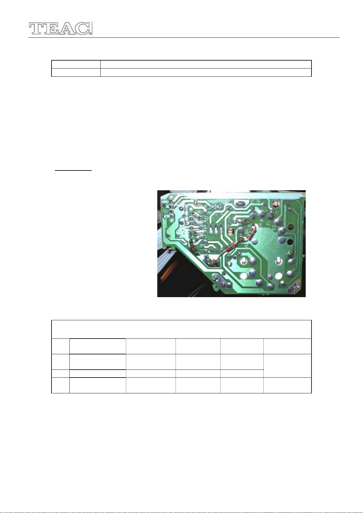
PROBLEM: Color purity problem
File: EU80 deg cap.doc
A missing capacitor in the degaussing circuit of some units can be the cause of poor color purity. The
problem is visible when displaying a red or a white test pattern field.
Instructions
1. Check if a 100nF 275 V AC capacitor is connected in parallel
with the degaussing coil. This component should be located
on the solder side of the auxiliary PCB where the degaussing
thermistor is mounted.
2. If the capacitor mentioned in step 1 is missing, connect a
100nF 275 V AC capacitor to the terminals of the degaussing
coil connector PL201
Regards,
Alcides Berta
TEAC Australia Pty Ltd.
Page 1 of 1

TECHNICAL BULLETIN 1-March-2000
MODEL: EU-80ST
PROBLEM: Color purity problem
File: EU80 deg cap.doc
A missing capacitor in the degaussing circuit of some units can be the cause of poor color purity. The problem
is visible when displaying a red or a white test pattern field.
Instructions
1. Check if a 100nF 275 V AC capacitor is connected in parallel
with the degaussing coil. This component should be located
on the solder side of the auxiliary PCB where the degaussing
thermistor is mounted.
2. If the capacitor mentioned in step 1 is missing, connect a
100nF 275 V AC capacitor to the terminals of the degaussing
coil connector PL201
Regards,
Alcides Berta
TEAC Australia Pty Ltd.
Page 1 of 1

TECHNICAL BULLETIN 02-Jun-00
MODEL:
PROBLEM:
EU-51/80 ST
Power supply problem
File: EU51-80 chopper tb.doc
The chopper transistor Q802 is damaged as a consequence of a fault in D816. This problem normally
occurs when a diode type UF5407 is used in the position D816.
Instructions
Replace damaged components. Use only a diode type BMY36D for the position D816.
Regards,
Alcides Berta
TEAC Australia Pty Ltd.
Page 1 of 1
TECHNICAL BULLETIN 26-Jun-00
MODEL:
PROBLEM: CRT output IC protection
EU 51 / 66 / 68 / 80 ST
File: EU51-80 spgap tb.doc
This is a tentative solution to avoid damages to the output video amplifier IC901 (TDA6107) caused by
electric discharges between electrodes of the CRT. The modification should be applied to units found
with damaged video amplifier IC.
Instructions
Add the following components to the
CRT board. Refer to the figure and
table below for parts location and
specifications.
Components information
Item Part Number Description From To Comments
1 EUSPARK 300V Spark gap Point G Aqua
2 EUSPARK 300V Spark gap Ground Aqua
3 QDTBOUZ6R2BS Zenner diode
6V2 400 mW
Regards,
Alcides Berta
TEAC Australia Pty Ltd.
1-PL901
(Cathode)
Page 1 of 1
Ground
(Anode)
Spark gap
devices have no
polarity

1
DO NOT CHANGE ANY MODULE UNLESS THE SET IS SWITCH OFF
The mains supply side of the switch mode power supply transformer is live.
Use an isolating transformer.
The receivers fulfill completely the safety requirements.
Safety precautions:
Servicing of this TV should only be carried out by a qualified person.
- Components marked with the warning symbol on the circuit diagram are critical for safety and must only be replaced with an identical
component.
- Power resistor and fusable resistors must be mounted in an identical manner to the original component.
- When servicing this TV, check that the EHT does not exceed 26kV.
TV Set switched off:
Make short-circuit between HV-CRT clip and CRT ground layer.
Short C804 (150mF) before changing IC802 or other components in primary side of SMPS.
Measurements:
Voltage readings and oscilloscope traces are measured under following conditions.
Antenna signal 60dB from colourbar generator. (100% white, 75% colour saturation)
Brightness, contrast, colour set for a normal picture.
Mains supply, 220VAC, 50Hz.
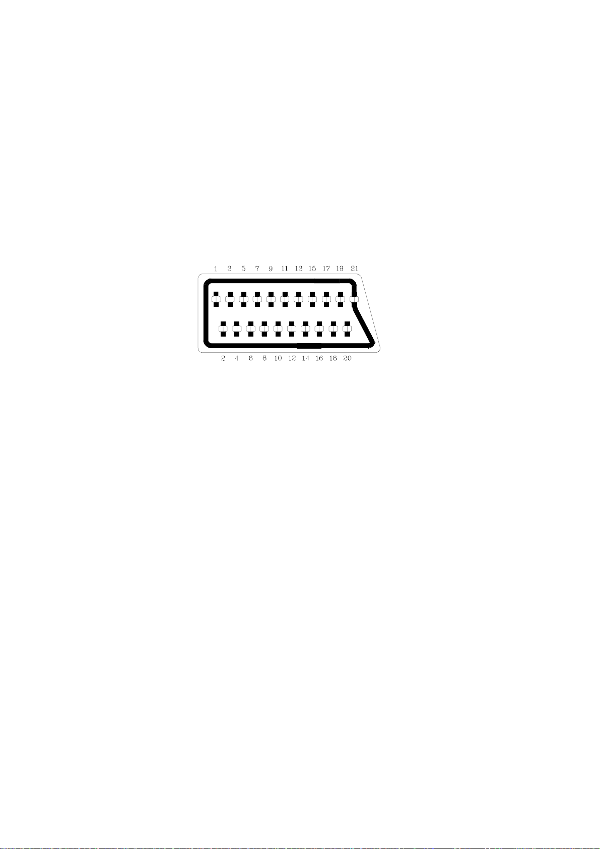
PERI-TV SOCKET
SCART 1 (SC050) SCART 2 (SC051)
1 Audio right output 0.5Vrms / 1K 1 Audio right output 0.5Vrms / 1K
2 Audio right input 0.5Vrms / 10K 2 Audio right input 0.5Vrms / 10K
3 Audio left output 0.5Vrms / 1K 3 Audio left output 0.5Vrms / 1K
4 Ground AF 4 Ground AF
5 Ground Blue 5 Ground Blue
6 Audio left input 0.5Vrms / 10K 6 Audio left input 0.5Vrms / 10K
7 Blue input 0.7Vpp / 75ohm 7 Blue input 0.7Vpp / 75ohm
8 AV switching input 0-12VDC /10K 8 AV switching input 0-12VDC /10K
9 Ground Green 9 Ground Green
10 - 10 11 Green input 0.7Vpp / 75ohm 11 12 - 12 13 Ground Red 13 Ground Red
14 Ground Blanking 14 Ground Blanking
15 Red input 0.7Vpp / 75ohm 15 16 Blanking input 0-0.4VDC, 1-3VDC / 75ohm 16 17 Ground CVS output 17 Ground CVS output
18 Ground CVS input 18 Ground CVS input
19 CVS output 1Vpp / 75ohm 19 CVS output 1Vpp / 75ohm
20 CVS input 1Vpp / 75ohm 20 CVS input 1Vpp / 75ohm
21 Ground 21 Ground
* * ALL WIRES TO FRONT PANEL & LOUD SPEAKERS MUST BE ZIP-TIED TOGETHER AFTER ANY KIND OF REPAIREMENT
1. INTRODUCTION
11AK19 is a 90ø and 110ø chassis capable of driving 20-21,24,25,28-29,32,33 tubes at appropriate currents.
The chassis is capable of working in both PAL and SECAM. The sound system is capable of giving 6watts
RMS output into a load of 8ohms.
One 8 page simple TELETEXT, TOPTEXT and FASTEXT is provided.
The chassis is equipped with 21-pin scart connectors which can accept via scart the SVHS format from VCRs so equipped.
2. SMALL SIGNAL PART WITH TDA884X
The TDA8840/8842/8844 combine all small signal functions required for a colour TV receiver, except tuning.
2.1. Vision IF amplifier
The IF-amplifier contains 3 AC-coupled control stages with a total gain control range which is higher than 66dB.
The sensitivity of the circuit is comparable with that of modern IF-IC s. The video signal is demodulated by means of a PLL
carrier regenerator. This circuit contains a frequency detector and a phase detector. The AFC output is obtained by using the
VCO control voltage of the PLL and can be read via the I²C-bus. For fast search tuning systems the window of
the AFC can be increased with a factor 3. The setting is realised with the AFW bit.
Depending on the type the AGC-detector operates on top-sync level (single standard versions) or on top sync and top
white-level (multi standard versions). The demodulation polarity is switched via the I²C-bus. The AGC detector time-constant capacitor
is connected externally. This mainly because of the flexibility of the application. The time-constant of the AGC system during positive
2

modulation is rather long to avoid visible variations of the signal amplitude. To improve the speed of the AGC system a circuit has
been included which detects whether the AGC detector is activated every frame period. When during 3 frame periods no action is
detected the speed of the system is increased. For signals without peak white information the system switches automatically to a
gated black level AGC. Because a black level clamp pulse is required for this way of operation the circuit will only switch to black level
AGC in the internal mode.
The circuits contain a video identification circuit which is independent of the synchronisation circuit. Therefore search tuning is
possible when the display section of the receiver is used as a monitor. The ident output is supplied to the tuning system via
the I²C-bus. The video ident circuit can be made less sensitive by means of the STM bit. This mode can be used during search tuning
to avoid that the tuning system will stop at very weak input signals.
2.2. Video Switches
The circuits have two CVBS inputs (internal and external CVBS) and Y/C input. When the Y/C input is not required the Y input can be
used as third CVBS input. The selection of the various sources is made via the I²C-bus. The circuit has one CVBS output.
2.3. Sound Circuit
The sound band pass and trap filters have to be connected externally. The filtered intercarrier signal is fed to a limiter circuit
and is demodulated by means of a PLL demodulator. This PLL circuit tunes itself automatically to the incoming carrier signal
so that no adjustment is required.
The volume is controlled via the I²C-bus. The deemphasis capacitor has to be connected externally. The non-controlled audio
signal can be obtained from this pin. The FM demodulator can be muted via the I²C-bus. This function can be used to switch-off
the sound during a channel change so that high output peaks are prevented. The TDA8840/8842 contain an automatic volume
levelling (AVL) circuit which automatically stabilises the audio output signal to a certain level which can be set by the viewer by means
of the volume control. This function prevents big audio output fluctuations due to variations of the modulation depth of the transmitter.
The AVL function can be activated via the I²C-bus.
2.4. Synchronisation circuit
The sync seperator is preceded by a controlled amplifier which adjusts the sync pulse amplitude to a fixed level. These pulses are fed
to the slicing stage which is operating at 50% of the amplitude. The separated sync pulses are fed to the first phase detector and to the
coincidence detector. This coincidence detector is used to detect whether the line oscillator is synchronised and can also be used for
transmitter identification. The first PLL has a very high statical steepness so that the phase of the picture is independent of the line
frequency.
The horizontal output signal is generated by means of an oscillator which is running at twice the line frequency. Its frequency is divided
by 2 to lock the first control loop to the incoming signal. The time-constant of the loop can be forced by the I²C-bus (fast or slow).
If required the IC can select the time-constant depending on the noise content of the incoming video signal.
To protect the horizontal output transistor, the horizontal drive is immediately switched off when a power-on-reset is detected.
The drive signal is switched-on again when the normal switch-on procedure is followed.
Via the I²C-bus, adjustments can be made of the horizontal and vertical geometry. The vertical sawtooth generator drives the
vertical output drive circuit which has a differrential output current. For the EW drive a single ended current output is available.
When the horizontal scan is reduced to display 4 : 3 pictures on a 16 : 9 picture tube an accurate video blanking can be switched on
to obtain well defined edges on the screen.
Overvoltage conditions can be detected via the EHT tracking pin.When an overvoltage condition is detected the horizontal output
drive signal will be switched-off via the slow stop procedure but it is also possible that the drive is not switched-off and that just a
protection indication is given in the I²C-bus output byte. The choice is made via the input bit PRD.
2.5. Chroma and Luminance processing
The circuits contain a chroma bandpass and trap circuit. The filters are realised by means of gyrator circuits and they are
automatically calibrated by comparing the tuning frequency with the X-tal frequency of the decoder.
The luminance delay line and the delay for the peaking circuit are also realised by means of gyrator circuits.
The centre frequency of the chroma bandpass filter is switchable via the I²C-bus so that the performance can be optimised for
front-end signals and external CVBS signals.
During SECAM reception the centre frequency of the chroma trap is reduced to get a better suppression of the SECAM
carrier frequencies.
2.6. Colour Decoder
The decoder contains an alignment-free X-tal oscillator, a killer circuit and two colour difference demodulators. The 90° phase shift for
the reference signal is made internally.
The IC contains an automatic colour limiting (ACL) circuit which prevents that oversaturation occurs when signals with a high
chroma-to-burst ratio are received. The ACL circuit is designed such that it only reduces the chroma signal and not the burst signal.
This has the advantage that the colour sensitivity is not affected by this function.
The base-band delay line is integrated in the PAL/SECAM IC s.
The demodulated colour difference signals are internally supplied to the delay line. The matrixed signals are externally available.
The colour difference matrix switches automatically between
PAL/SECAM and NTSC, however, it is also possible to fix the matrix in the PAL standard.
Which colour standard the IC can decode depends on the external X-tals. The X-tal to be connected to pin 34 must have a frequency
of 3.5 MHz (NTSC-M, PAL-M or PAL-N) and pin 35 can handle X-tals with a frequency of 4.4 and 3.5 MHz. To prevent calibration
problems of the horizontal oscillator the external switching between the 2 X-tals should be carried out when the oscillator is forced to
pin 35. For a reliable calibration of the horizontal oscillator it is very important that the X-tal indication bits (XA and XB) are not
corrupted. For this reason the X-tal bits can be read in the output bytes so that the software can check the I²C-bus transmission.
2.7. RGB output circuit and black-current stabilisation
The colour-difference signals are matrixed with the luminance signal to obtain the RGB-signals. The TDA 884X device has one linear
RGB input. This RGB signal can be controlled on contrast and brightness.
The output signal has an amplitude of about 2 volts black-to-white at nominal input signals and nominal settings of the controls.
To increase the flexibility of the IC it is possible to insert OSD and/or teletext signals directly at the RGB outputs.
This insertion mode is controlled via the insertion input (pin 26 in the S-DIP 56- and pin 38 in the QFP-64 level). This blanking action
at the RGB outputs has some delay which must be compansated externally.
To obtain an accurate biasing of the picture tube a Continuous Cathode Calibration circuit has been developed.
This function is realised by means of a 2-point black level stabilisation circuit.
When the TV receiver is switched-on, the RGB output signals are blanked and the black current loop will try to set the right picture
tube bias levels.Via the AST bit a choice can be made between automatic start-up or a start-up via the m-processor.
3
3. TUNER
Either a PLL or a VST tuner is used as a tuner.
UV1316 (VHF/UHF) is used as a PLL tuner. For only PALM/N, NTSC M applications UV 1336 is used as the PLL tuner. UV 1315 (VHF/
UHF) is used as a VST Tuner.
Channel coverage of UV1316:
BAND
Low Band E2 to C 48.25 to 82.25 (1) S01 to S08 69.25 to 154.25
Mid Band E5 to E12 175.25 to 224.25 S09 to S38 161.25 to 439.25
High Band E21 to E69 471.25 to 855.25 (2) S39 to S41 447.25 to 463.25
(1). Enough margin is available to tune down to 45.25 MHz.
(2). Enough margin is available to tune up to 863.25 MHz.
OFF-AIR CHANNELS CABLE CHANNELS
CHANNELS FREQUENCY CHANNELS FREQUENCY
RANGE (MHz) RANGE (MHz)
Noise Typical Max. Gain Min. Typical Max.
Low band : 5dB 9dB All channels : 38dB 44dB 52dB
Mid band : 5dB 9dB Gain Taper (of-air channels) : - - 8dB
High band : 6dB 9dB
Channel Coverage UV1336:
BAND CHANNELS FREQUENCY
RANGE (MHz)
Low Band 2 to D 55.25 to 139.25
Mid Band E to PP 145.25 to 391.25
High Band QQ to 69 397.25 to 801.25
Noise is typically 6dB for all channels. Gain is minimum 38dB and maximum 50dB for all channels.
Channel Coverage of UV1315:
BAND
Low Band E2 to C 48.25 to 82.25 (1) S01 to S10 69.25 to 168.25
Mid Band E5 to E12 175.25 to 224.25 S11 to S39 231.25 to 447.25
High Band E21 to E69 471.25 to 855.25 (2) S40 to S41 455.25 to 463.25
(1). Enough margin is available to tune down to 45.25 MHz.
(2). Enough margin is available to tune up to 863.25 MHz.
Noise Typ. Max. Gain Min. Typ. Max.
Low band : 6dB 9dB All Channels 38dB 44dB 50dB
Mid band : 6dB 10dB Gain Taper - - 8dB
High band : 6dB 11dB (off-air channels)
4.VIDEO SWITCH TEA6415C
In case of three or more external sources are used, the video switch IC TEA6415C is used. The main function of this device is to switch
8 video input sources on the 6 outputs.
Each output can be switched on only one of each input. On each input an alignment of the lowest level of the signal is made (bottom
of sync. top for CVBS or black level for RGB signals).
Each nominal gain between any input and output is 6.5dB.For D2MAC or Chroma signal the alignment is switched off by forcing, with
an external resistor bridge, 5VDC on the input. Each input can be used as a normal input or as a MAC or Chroma input (with external
resistor bridge). All the switching possibilities are changed through the BUS.
Driving 75ohm load needs an external resistor.
It is possible to have the same input connected to several outputs.
OFF-AIR CHANNELS CABLE CHANNELS
CHANNELS FREQUENCY CHANNELS FREQUENCY
RANGE (MHz) RANGE (MHz)
5. AM DEMODULATOR TDA9830
The TDA9830 is designed for AM-sound demodulation used in L and L standard.
4

Sound IF Input:
The sound IF amplifier consists of three AC-coupled differential amplifier stages each with approximately 20dB gain.
At the output of each stage is a multiplier for gain controlling. The overall control range is approximately -6 to +60dB and the
frequency response (-3dB) of the IF amplifier is approximately 6 to 70MHz. The steepness of gain control is approximately 10mV/dB.
IF AGC:
The automatic gain control voltage to maintain the AM demodulator output signal at a constant level is generated by a mean
level detector.The AGC-detector charges and discharges the capacitor at pin 3 controlled by the output signal of the
AM-demodulator compared to an internal reference voltage.The maximum charge/discharge current is approximately 5 mA.
AM-demodulator
The IF amplifier output signal is fed to a limiting amplifier (two stages) and to a multiplier circuit.
However the limiter output signal (which is not any more AM modulated) is also fed to the multiplier, which provides AM
demodulation (in phase demodulation). After lowpass filtering (fg @ 400kHz) for carrier rejection and buffering,
the demodulator output signal is present at pin 6.
Audio Switch
This circuit is an operational amplifier with three input stages and internal feedback network determining gain (0dB) and
frequency response (fg @ 700kHz). Two of the input stages are connected to pin 7 and pin 9, the third input stage to an
internal reference voltage. Controlled by the switching pins 10 and 12, one of the three input stages can be activated and a
choice made between two different AF signals or mute state. The selected signal is present at pin 8. The decoupling capacitors
at the input pins are needed, because the internally generated bias voltage for the input stages must not be influenced
by the application in order to avoid DC-plop in case of switching.
Reference Circuit:
This circuit is a band gap stabiliser in combination with a voltage regulation amplifier, which provides an internal reference voltage
of about 3.6V nearly independent from supply voltage and temperature. This reference voltage is filtered by the capacitor at
pin 4 in order to reduce noise. It is used as a reference to generate all important voltages and currents of the circuit.
For application in 12V power supply concepts, there is an internal voltage divider in combination with a Darlington transistor in
order to reduce the supply voltage for all IC function blocks to approximately 6V.
6. DIGITAL TV SOUND PROCESSOR TDA9875
The TDA9875 is a single-chip Digital TV Sound Processor.
Supported standards are M, B/G, D/K, I and L.
Description of the demodulator and decoder section:
SIF Input:
Two input pins are provided, SIF1 e.g. for terrestrial TV and SIF2 e.g. for a satellite tuner. The selected signal is passed through an
AGC circuit and then digitized by an 8-bit ADC operating at 24.576MHz.
AGC:
The gain of the AGC amplifier is controlled from the ADC output by means of a digital control loop employing hysteresis.
The AGC has a fast attack behaviour to prevent ADC overloads and slow decay behaviour AGC oscillations.
For AM demodulation AGC must be switched off.
Mixer
The digitized input signal is fed to the mixers, which mix one or both input sound carriers down to zero IF. A 24-bit control word for
each carrier sets the required frequency.
FM and AM Demodulation
An FM or AM input signal is fed via a band-limiting filter to a demodulator that can be used for either FM or AM demodulation.
Apart from the standard (fixed) de-emphasis characteristic, an adaptive de-emphasis is available for encoded satellite programs.
A stereo decoder recovers the left and right signal channels from the demodulated sound carriers.
FM Identification:
The identification of the FM sound mode is performed by AM synchronous demodulation of the pilot signal and narrow-band detection
of the identification frequencies. The result is available via the I²C-bus interface.
NICAM Demodulation:
The NICAM signal is transmitted in a DQPSK code at a bit rate of 728 kbit/s. The NICAM demodulator performs DQPSK
demodulation and feeds the resulting bitstream and clock signal onto the NICAM decoder and, for evaluation purposes, to PCLK
(pin 1) and NICAM (pin 2).
NICAM Decoder:
The device performs all decoding functions in accordance with the EBU NICAM 728 specification. After locking to the frame
alignment word, the data is descrambled by applying the defined pseudo-random binary sequence; the device will then synchronise
to the periodic frame flag bit C0.
The status of the NICAM decoder can be read out from the NICAM status register by the user. The OSB bit indicates that the
decoder has locked to the NICAM data. The VDSP bit indicates that the decoder has locked to the NICAM data and that the
data is valid sound data.
7. SOUND OUTPUT STAGE TDA2614/TDA2615/TDA2616Q
TDA2614 is used as the AF output amplifier for mono applications. It is supplied by ±12VDC coming from a separate winding in the
SMPS transformer. An output power of 2*6W (THD=0.5%) can be delivered into an 8ohm load.
TDA2615 is used as the AF output amplifier for stereo applications. It is supplied by
±12VDC coming from a separate winding in the SMPS transformer. An output power of 2*6W (THD=0.5%)
can be delivered into an 8ohm load.
TDA2616Q is used as the AF output amplifier for stereo and dolby prologic applications. It is supplied by ±16VDC coming from
a separate winding in the SMPS transformer. An output power of 2*12W (THD=0.5%) can be delivered into an 8ohm load.
5

8. VERTICAL OUTPUT STAGE WITH TDA8351/8356
The TDA8351/8356 vertical deflection circuit can be used in 90° and 110° deflection systems with field frequencies from
50 up to 120Hz. With its bridge configuration the deflection output can be DC coupled with few external components.
Only a single supply voltage for the scan and a second supply for the flyback are needed. The TDA8356 is intended for 90°
systems and the TDA8351 is intended for 110° systems.
The drive voltage is amplified by an amplifier and fed to two amplifiers, one is inverting and the other is a non inverting amplifier.
The outputs (pins 7 and 4) are connected to the series connection of the vertical deflection coil and feedback resistor Rsense
(R702//R703). The voltage across Rsense is fed via pin 9 to correction amplifier, to obtain a deflection current which is proportional
to the drive voltage. The supply voltage for the TDA8351/8356 is 15VDC at pin 3. The supply voltage generator has a separate
supply voltage of 45VDC at pin 6.
9. VIDEO OUTPUT AMPLIFIER TDA6107Q
The TDA6107Q consists of three monolithic video output amplifiers. The amplifier can be seen as an operational amplifier
with negative feedback.
The advantage of negative feedback is that the amplifier characteristics do not play an important role up to certain frequencies.
The internal flash diodes protect the amplifiers against flash over in the picture tube.
The only protections required at the cathode outputs are a flash resistor and a sparkgap.
The TDA6107Q has an internal thermal protection circuit which gives a decrease of the slew rate at high temperatures.
Furthermore, the device needs only one power supply voltage (Vdd).
In contrast to previous types of DMOS video amplifiers, all the external resistors (Rf, Ri and Ra) are integrated, so the gain is fixed
and saves 9 resistors.
Furthermore, the reference voltage is integrated, it saves a resistor divider and a decoupling capacitor. So, the replacement
value of the TDA6107Q is very high.
The TDA6107Q is provided with a black current data pin. Since TDA884X is used as drive device, no adjustments are required
for gain and black setting, as the TDA884X has I²C white point adjustment and black current set-up.
10. SINGLE/MULTISTANDARD VIF/SIF-PLL and FM-PLL/AM
DEMODULATOR TDA9818
The TDA9818is an IC for multistandard vision IF signal processing, sound AM and FM demodulation.
It is a gain controlled wide band VIF-amplifier (AC-coupled). It is applicable for IF frequencies of 38.9 MHz, 45.75 MHz and 58.75 MHz.
True synchronous demodulation is provided with active carrier regeneration. It has a VCO frequency which can be switchable
between L and L accent (alignment external) picture carrier frequency.
The TDA9818 has a SIF input for single reference QSS mode (PLL controlled). SIF AGC detector is to provide gain controlled
SIF amplifier. The AM demodulator is without extra reference circuit. The supply voltage is +5VDC at pin 21.
11. COMBFILTER SAA4961
The SAA 4961 is a one-chip, PAL/NTSC combfilter IC with internal delay lines, filters, clock control, synchronisation and
signal switches. The combfilter function is realised in a switched capacitor technique, so it has time discrete but amplitude
continuous processing.
The Y/CVBS input is first clamped and then fed to the delay-line and combfilter section via a low pass pre-filter.
This filter can be bypassed via the external LPF-on pin. This pin is internally pulled up, to put the filter default on. The Y/CVBs
input is also fed to the sync seperator, where horizontal and vertical reference pulses are made.
Bypass mode can be forced via BYP (pin 3).FSC (pin 1) is the subcarrier input which is connected to the colour decoder.
Input FSCSW pin indicates if fsc or 2*fsc is used.
The Sys1,2 pins (20, 23) indicate which system standard is processed. Sys2 is internally pulled up, Sys1 is internally pulled down.
Therefore when the Sys1,2 inputs are left open, automatically PAL 4.43MHz is forced.
SAA4961output pin 15 CVBS can be used for parallel-synced teletext decoders, to guarantee that the teletext display always
has a correct timing relation with the main picture. Comb filter is disabled by setting SAA4961 pin 3 BYP high.
12. POWER SUPPLY (SMPS)
The DC voltages required at various parts of the chassis are provided by an SMPS transformer controlled by the IC MC44604
which is designed for driving, controlling and protecting switching transistor of SMPS. The transformer produces 150/115V for
FBT input, ±14V for audio output IC, S+5V for microcontroller, +15V for vertical output (field scan) and +33V for tuner and some
other ICs and transistors.
13. MICROCONTROLLER SDA525X
The device is TV TEXT tuning and control system based on the SDA 525X TV TEXT microcontroller. It is designed for a low
cost mono TV-SET with analogue picture and sound control. Neverthless the system offers an on screen display (OSD) and
IR remote control of all functions.
SDA525X has the following features:
- Display of program number, channel number, TV standard, analogue values, sleep timer, parental control, and mute is done by OSD.
- Single LED for IR active, standby and on mode indication.
- 1 Control line to select external source.
- 3 Control lines for TV standard selection.
- Frequency synthesis tuning (62.5 kHz steps)
- 192 step fine tuning
- Channels corresponding to standards B/G, OIRT, L and I (I+)
- Mono sound control by analogue voltage
- System configuration with service mode
14. SERIAL ACCESS CMOS 8K (1024*8) EEPROM ST24C08
The ST24C08 is a 8Kbit electrically erasable programmable memory (EEPROM), organised as 4 blocks of 256*8 bits.
The memory is compatible with the I²C standard, two wire serial interface which uses a bi-directional data bus and serial clock.
The memory carries a built-in 4 bit, unique device identification code (1010) corresponding to the I²C bus definition.
This is used together with 1 chip enable input (E) so that up to 2*8K devices may be attached to the I²C bus and selected individually.
6

15. CLASS AB STEREO HEADPHONE DRIVER
The TDA1308 is an integrated class AB stereo headphone driver contained in a DIP8 plastic package.
The device is fabricated in a 1 mm CMOS process and has been primarily developed for portable digital audio applications.
16. SAW FILTERS
Saw filter type : Model:
G1965M : PAL-SECAM B/G MONO
G3962M : PAL-SECAM B/G GER&NIC STEREO, PAL I NIC STEREO, INT-1
G1984 : PAL-SECAM B/G GER&NIC STEREO INT-2
J1951M : PAL-I MONO
J3950M : PAL-I NIC STEREO
J1956M : PAL-I MONO
K2955M : PAL-SECAM B/G-D/K MONO, PAL-SECAM B/G-D/K-I, MONO, PAL-SECAM B/G-D/K-L MONO
K2958M : PAL-SECAM B/G-D/K (38) MONO
K2962M : PAL-SECAM B/G-L/L MONO
G3957M : PAL-SECAM B/G-L/L GER&NIC BG/L STEREO
K6256K : PAL-SECAM B/G-D/K-I-L/L MONO, PAL-SECAM B/G-D/K-I, L/L GER&NIC BG/L STEREO,
PAL-SECAM B/G-D/K-I-L/L I, NICAM STEREO, PAL-SECAM B/G-D/K-I-L/L GER&NIC I-B/G-L, STEREO
K6259K : PAL-SECAM B/G-D/K-I-M/N (EURO) MONO
M1963M : PAL M/N MONO, NTSC M MONO, PAL M/N-NTSC M MONO
17. BTSC STEREO/SAP/DBX-DECODER and AUDIO PROCESSOR TDA9855
The TDA9855 is a BTSC stereo/SAP/dbx decoder and audio processor. It performs all functions to transform the composite baseband
signal into the appropriate audio output signals to line out and to the loudspeaker output stages.
IC DESCRIPTIONS AND INTERNAL BLOCK DIAGRAM
n TDA8840/8842/8844
n TUNER (UV1315, UV1316, UV1336)
n TEA6415C
n TDA9830
n TDA2614/2615/2616Q
n TDA8351/8356
n TDA6107Q
n SAA4961
n MC44604
n SDA525X
n TDA9875
n TDA9818
n ST24C08
n TDA1308
n G1965M
n TDA9855
TDA1308
TDA8840/8842/8844:
The TDA884X is IýC-bus controlled single chip TV processor which is intended to be applied in PAL, NTSC, PAL/NTSC and
multi-standard television receivers. These IC s are nearly pin compatible with the TDA837X TV processors but have a higher
degree of integration because the delay line (TDA4665 function) and the SECAM decoder have been integrated. In addition to
these functions some additional features have been added like Continuous Cathode Calibration (2-point black current loop
which results in an accurate biasing of the 3 guns), adjustable luminance delay time, blue stretching and dynamic skin tone control.
Features:
n Vision IF circuit with PLL demodulator
n Alignment-free multi-standard FM sound demodulator (4.5 MHz to 6.5 MHz)
n Audio switch
n Flexible source selection with CVBS switch and Y(CVBS)/C input so that a comb filter can be applied
n Integrated chrominance trap circuit
n Integrated luminance delay line
n Asymmetrical peaking in the luminance channel with a noise coring function
n Black stretching of non-standard CVBS or luminance signals
n Integrated chroma band-pass filter with switchable center frequency
n Blue stretch circuit which offsets colours near white towards blue
n RGB control circuit with Continuous Cathode Calibration and white point adjustment
n Linear RGB inputs and fast blanking
n Possibility to insert a blue black option when no video signal is available
n Horizontal synchronisation with two control loops and alignment-free horizontal oscillator
n Vertical count-down circuit
n Vertical driver optimised for DC-coupled vertical output stages
n IýC-bus control of various functions
n Low dissipation (850 mW)
Functional Differences between the 8840/8842/8844:
7

IC VERSION (TDA) 8840 8842 8844
Multi-standard IF X X
Automatic Volume Limiting X X
PAL Decoder X X X
SECAM Decoder X X
NTSC Decoder X X
Dynamic Skin Control X
Colour Matrix PAL/NTSC (Japan) X X
Colour Matrix NTSC Japan/USA
YUV interface X
Base-band delay line X X X
Adjustable luminance delay time X
Horizontal geometry X
Horizontal and vertical zoom X
Vertical scroll X
PINNING PIN VALUE
1. Sound IF input : 1mVrms
2. External audio input : 500mVrms
3. IF demodulator tuned circuit 1
4. IF demodulator tuned circuit 2
5. IF-PLL loop filter : Min:32-Max:60 MHz
6. IF video output : 4.7V (Negative Modulation), 2V (Positive Modulation)
7. Serial clock input : Low level max:1.5 V, High level min 3.5V
8. Serial data input/output : Low level max:1.5 V, High level min 3.5V
9. Bandgap decoupling
10. Chrominance input (S-VHS) : 1Vpp, Max:1.4Vpp
11. External CVBS/Y input : 1Vpp, Max:1.4Vpp
12. Main supply voltage 1 : 8V, Min:7.2V, Max:8.8V
13. Internal CVBS input : 1Vpp, Max:1.4Vpp
14. Ground 1
15. Audio output : 700mVrms, Min:500mVrms, Max:900mVrms
16. SECAM PLL decoupling
17. External CVBS input : Vpp, Max:1.4Vpp
18. Black-current input : Amplitude of low reference current : 8mA
Amplitude of high reference current : 20mA
19. Blue output : 2Vpp
20. Green output : 2Vpp
21. Red output : 2Vpp
22. Beam current limiter input/V-guard input
23. Red input for insertion : 0.7Vpp, Max:0.8Vpp
24. Green input for insertion : 0.7Vpp, Max:0.8Vpp
25. Blue input for insertion : 0.7Vpp, Max:0.8Vpp
26. RGB insertion input : Max:0.3V
27. Luminance input : 1.4Vpp
28. Luminance output : 1.4Vpp
29. (B-Y) signal output : 1.05Vpp
30. (R-Y) signal output : 1.05Vpp
31. (B-Y) signal input : 1.05Vpp
32. (R-Y) signal input : 1.05Vpp
33. Subcarrier reference output : 3.58/4.43 MHz
34. 3.58 MHz crystal connection
35. 4.43/3.58 MHz crystal connection
36. Loop filter phase detector
37. 2nd
supply voltage 1 : 8V, Min:7.2V, Max:8.8V
38. CVBS output : 1Vpp, Max:1.4Vpp
39. Decoupling digital supply : 1.8V
40. Horizontal output : Max: 0.3V
41. Flyback input/sandcastle output : Min:100ma, Max:300mA
42. Phase-2 filter : 150 ms/ms
43. Phase-1 filter : ±0.9 kHz, Max: ±1.2 kHz
44. Ground 2
45. East-west drive output
46. Vertical drive A output : 0.95mA
47. Vertical drive B output : 0.95mA
48. IF input 1
49. IF input 2
50. EHT/overvoltage protection input : Min:1.2V, Max : 2.8V
51. Vertical sawtooth capacitor : 3Vpp
52. Reference current input : 3Vpp
53. AGC decoupling capacitor
54. Tuner AGC output : Max:9V (Maximum tuner AGC
output voltage), 300mV (Output saturation voltage)
55. Audio deemphasis : 500mVrms
56. Decoupling sound demodulator
8

UV1315, UV1316, UV1336
General description of UV1315:
The UV1315 tuner belongs to the UV 1300 familiy of tuners, which are designed to meet a wide range of applications.
It is a combined VHF, UHF tuner suitable for CCIR systems B/G, H, L, L, I and I. The low IF output impedance has been
designed for direct drive of a wide variety of SAW filters with sufficient suppression of triple transient.
Features of UV1315:
n Member of the UV1300 family small sized UHF/VHF tuners
n Systems CCIR:B/G, H, L, L, I and I; OIRT:D/K
n Voltage synthesized tuning (VST)
n Off-air channels, S-cable channels and Hyperband
n Standardized mechanical dimensions and pinning
n Compact size
PINNING PIN VALUE
1. Gain control voltage (AGC) : 4.0V, Max:4.5V
2. Tuning voltage
3. High band switch : 5V, Min:4.75V, Max:5.5V
4. Mid band switch : 5V, Min:4.75V, Max:5.5V
5. Low band switch : 5V, Min:4.75V, Max:5.5V
6. Supply voltage : 5V, Min:4.75V, Max:5.5V
7. Not connected
8. Not connected
9. Not connected
10. Symmetrical IF output 1
11. Symmetrical IF output 2
Bandswitching table:
Pin 3 Pin 4 Pin 5
Low band 0V 0V +5V
Mid band 0V +5V 0V
High band +5V 0V 0V
General description of
The UV1316 tuner belongs to the UV 1300 family of tuners, which are designed to meet a wide range of applications.
It is a combined VHF, UHF tuner suitable for CCIR systems B/G, H, L, L, I and I. The low IF output impedance has been designed
for direct drive of a wide variety of SAW filters with sufficient suppression of triple transient.
Features of UV1316:
n Member of the UV1300 family small sized UHF/VHF tuners
n Systems CCIR: B/G, H, L, L, I and I; OIRT: D/K
n Digitally controlled (PLL) tuning via IýC-bus
n Off-air channels, S-cable channels and Hyperband
n World standardized mechanical dimensions and world standard pinning
n Compact size
n Complies to CENELEC EN55020 and EN55013
PINNING PIN VALUE
1. Gain control voltage (AGC) : 4.0V, Max:4.5V
2. Tuning voltage
3. I²C-bus address select : Max:5.5V
4. I²C-bus serial clock : Min:-0.3V, Max:5.5V
5. I²C-bus serial data : Min:-0.3V, Max:5.5V
6. Not connected
7. PLL supply voltage : 5.0V, Min:4.75V, Max:5.5V
8. ADC input
9. Tuner supply voltage : 33V, Min:30V, Max:35V
10. Symmetrical IF output 1
11. Symmetrical IF output 2
UV1316:
General description of
UV1336 series is developed for reception of channels broadcast in accordance with the M, N standard. The tuning is available
through built-in digitally controlled IýC bus (PLL).
Features of UV1336:
n Global standard pinning
n Integrated Mixer-Oscillator&PLL function
n Conforms to CISPR 13, FCC and DOC (Canada) regulations
n Low power consumption
n Both Phono connector and F connector are available
UV1336:
9

PINNING PIN VALUE
1. Gain control voltage : 4.0V, Max:4.5V
2. Tuning voltage
3. Address select : Max:5.5V
4. Serial clock : Min:-0.3V, Max:5.5V
5. Serial data : Min:-0.3V, Max:5.5V
6. Not connected
7. Supply voltage : 5.0V, Min:4.75V, Max:5.5V
8. ADC input (optional)
9. Tuning supply voltage : 33V, Min:30V, Max:35V
10. Ground
11. IF output
TEA6415C:
General Description:
The main function of the TEA6415C is to switch 8 video input sources on the 6 outputs.
Each output can be switched to only one of the inputs whereas but any same input may be connected to several outputs.
All switching possibilities are controlled through the IýC-bus.
Features:
n 20 MHz Bandwith
n Cascadable with another TEA6415C (Internal address can be changed by pin 7 voltage)
n 8 inputs (CVBS, RGB, Mac, CHROMA, )
n 6 Outputs
n Possibility of MAC or chroma signal for each input by switching-off the clamp with an external resistor bridge
n Bus controlled
n 6.5dB gain between any input and output
n -55dB crosstaljk at 5MHz
n Fully ESD protected
PINNING PIN VALUE
1. Input : Max : 2Vpp, Input Current : 1mA, Max : 3mA
2. Data : Low level : -0.3V Max:1.5V, High level : 3.0V Max : Vcc+0.5V
3. Input : Max : 2Vpp, Input Current : 1mA, Max : 3mA
4. Clock : Low level : -0.3V Max:1.5V, High level : 3.0V Max : Vcc+0.5V
5. Input : Max : 2Vpp, Input Current : 1mA, Max : 3mA
6. Input : Max : 2Vpp, Input Current : 1mA, Max : 3mA
7. Prog
8. Input : Max : 2Vpp, Input Current : 1mA, Max : 3mA
9. Vcc : 12V
10. Input : Max : 2Vpp, Input Current : 1mA, Max : 3mA
11. Input : Max : 2Vpp, Input Current : 1mA, Max : 3mA
12. Ground
13. Output : 5.5Vpp, Min : 4.5Vpp
14. Output : 5.5Vpp, Min : 4.5Vpp
15. Output : 5.5Vpp, Min : 4.5Vpp
16. Output : 5.5Vpp, Min : 4.5Vpp
17. Output : 5.5Vpp, Min : 4.5Vpp
18. Output : 5.5Vpp, Min : 4.5Vpp
19. Ground
20. Input : Max : 2Vpp, Input Current : 1mA, Max : 3mA
TDA9830:
General description:
The TDA9830, a monolithic integrated circuit, is designed for AM-sound demodulation used in L- and L-standard.
The IC provides an audio source selector and also mute switch.
Features:
n Adjustment free wideband synchronous AM demodulator
n Audio source-mute switch (low noise)
n Audio level according EN50049
n 5 to 8V power supply or 12 V alternative
n Low power consumption
PINNING PIN VALUE
1. Sound IF differential input signal : Minimum IF input signal (between pins 1 and 16):60mV
Max:100mV Maximum IF input signal (between pins 1 and 16) :120mV Min :70mV
2. Not connected
3. AGC capacitor
4. REF voltage filtering capacitor
5. Not connected
6. AM demodulator output : THD:0.8%, Max:2%; S/N:53dB, Min:47%; DC potential:2.15V, Min : 2.00V Max :2.30V
7. Input signal (from AM) to audio switch : Max:1.2V
8. Output signal from audio switch : 80dB, Min : 70dB
9. Input signal (from external) to audio switch : Max:1.2V
10

10. Switch input select control : Audio switching voltage to activate pin7 : Min :0V, Max :0.8V
Audio switching voltage to activate pin9 : Min:1.5V, Max :Vp
11. Supply voltage : 12V, Min:10.8V, Max:13.2V
12. Mute control : For Mute-ON Min : 0V, Max : 0.8V For Mute-OFF Min : 1.5V, Max : Vp
13. Ground
14. Supply voltage : 5V, Min : 4.5V, Max : 8.8V
15. Not connected
16. Sound IF differential input signal : Look at pin 1
TDA2614/TDA2615/TDA2616Q:
General Description of TDA2614:
The TDA2614 is a power amplifier in a 9-lead single-in-line (SIL9) plastic medium power package. It has been especially
designed for mains fed applications.
Features:
n Requires very few external components
n No switch-on/switch-off clicks
n Input mute during switch-on and switch-off
n Low offset voltage between output and ground
n Hi-fi in accordance with IEC 268 and DIN 45500
n Short-circuit proof and thermal protected
n Mute possibility
PINNING PIN VALUE
1. Not connected
2. Mute input : 300mA (For mute to activate)
3. Ground
4. Not connected
5. Supply voltage (negative) : -12VDC
6. Output : 6.9Vrms
7. Supply voltage (positive) : +12VDC
8. Inverting input (Ground) : 0V
9. Non-inverting input : 700mVrms, Min : 500mVrms, Max : 900mVrms
General Description of
The TDA2615 is a dual power amplifier in a 9-lead single-in-line (SIL9). It has been especially designed for mains fed applications.
Features:
n Requires very few external components
n No switch-on/switch-off clicks
n Input mute during switch-on and switch-off
n Low offset voltage between output and ground
n Excellent gain balance of both amplifiers
n Hi-fi in accordance with IEC 268 and DIN 45500
n Short-circuit proof and thermal protected
n Mute possibility
PINNING PIN VALUE
1. Non-inverting input 1 : 700mVrms, Min :500mVrms, Max : 900mVrms
2. Mute input : 300mA (For mute to activate)
3. Ground
4. Output 1 : 6.9Vrms
5. Supply voltage (negative) : -12VDC
6. Output 2 : 6.9Vrms
7. Supply voltage (positive) : +12VDC
8. Inverting inputs 1 and 2 (Ground) : 0V
9. Non-inverting input 2 : 700mVrms, Min : 500mVrms, Max : 900mVrms
General Description of
The TDA2616Q is a dual power amplifier. It is supplied in a 9-lead SIL-bent-to DIL plastic power package (SOT157).
It has been especially designed for mains fed applications.
TDA2615:
TDA2616Q:
Features:
n Requires very few external components
n No switch-on/switch-off clicks
n Input mute during switch-on and switch-off
n Low offset voltage between output and ground
n Excellent gain balance of both amplifiers
n Hi-fi in accordance with IEC 268 and DIN 45500
n Short-circuit proof and thermal protected
n Mute possibility
11

PINNING PIN VALUE
1. Non-inverting input 1 : 700mVrms, Min : 500mVrms, Max : 900mVrms
2. Mute input : 300mA (For mute to activate)
3. Ground
4. Output 1 : 9.8Vrms
5. Supply voltage (negative) : -16VDC
6. Output 2 : 9.8Vrms
7. Supply voltage (positive) : +16VDC
8. Inverting inputs 1 and 2 (Ground) : 0V
9. Non-inverting input 2 : 700mVrms, Min : 500mVrms, Max : 900mVrms
TDA8351/8356:
General Description:
The TDA8356 is a power circuit for use in 90ø colour deflection system for field frequencies of 50 to 120 Hz.
The circuit operates as a highly efficient class G system.
The TDA8351 is a power circuit for use in 110ø colour deflection system for field frequencies of 50 to 120 Hz.
The circuit operates as a highly efficient class G system.
Features:
n Few external components
n Highly efficient fully DC-coupled vertical output bridge circuit
n Vertical flyback switch
n Guard circuit
n Protection against:
- short-circuit of the output pins (7 and 4)
- short-circuit of the output pins to Vp
n Temperature (thermal) protection
n High EMC immunity because of common mode inputs
n A guard signal in zoom mode
PINNING PIN VALUE
1. Input power-stage (positive); includes Ii(sb) signal bias : 400mA, Min : 50mA, Max : 500mA
2. Input power-stage (negative); includes Ii(sb) signal bias : 400mA, Min : 50mA, Max : 500mA
3. Operating supply voltage : +15VDC
4. Output voltage B : Max : 52V Output current : 2App (TDA8356) 3App (TDA8351)
5. Ground
6. Input flyback supply voltage : Min : Vp, Max : 50V
7. Output voltage A : Max : 52V Output current : 2App (TDA8356) 3App (TDA8351)
8. Guard output voltage : Max:5.5V (Io:100mA)
9. Input feedback voltage : Max:52V
TDA6107Q:
The TDA6107Q includes three video output amplifiers in a SIL 9 MP (Single In Line 9 pins Medium Power) package SOT111BE,
using high-voltage DMOS technology, and is intended to drive the three cathodes of a colour picture tube.
In contrast to previous types of DMOS video amplifiers, all external resistors (Rf, Ri and Ra) are integrated, so the gain is fixed
and it saves 9 resistors.
To obtain maximum performance, the amplifier should be used with black-current control and mounted on the CRT panel.
Features:
n Bandwith: 4.0 MHz typ at 100Vpp (Measured in appli,cation set-up, with Rfl=1K5 and Cl=Ctube+Cpcb=10pF)
n Slewrate: 950V/ms
n Fixed gain of 50 times
n No external components, only the well known supply decoupling
n Very simple application with a variety of colour decoders
n Black-current measurement output for automatic black current stabilization
n Only one supply voltage needed
n Internal protection against positive appearing CRT flash-over discharges
n Protection against ESD
n Internal reference voltage
n Thermal protection
n Controllable switch-off behaviour
n Very small PCB dimensions
n Very high replacement value
PINNING PIN VALUE
1. Inverting input 1 : 2Vpp
2. Inverting input 2 : 2Vpp
3. Inverting input 3 : 2Vpp
4. Ground
5. BSC-output : Max:7V
6. Supply voltage : 200VDC
7. Cathode output 3 : 20mA, 100Vpp
8. Cathode output 2 : 20mA, 100Vpp
9. Cathode output 1 : 20mA, 100Vpp
12

SAA4961:
The SAA4961 is an adaptive alignment-free one chip comb filter compatible with both PAL and NTSC systems and provides high
performance in Y/C separation.
Features:
n One chip adaptive multi-standard comb filter
n Time discrete but continuous amplitude signal processing with analogue interfaces
n Internal delay lines, filters, clock processing and signal switches
n Alignment-free
n No hanging dots or residual cross colour on vertical transients
n Few external components
It is possible to switch the comb filter into one of the following 3 modes:
1. Comb mode : In this mode, luminance and chrominance comb filter function are active.
Chrominance output pin (pin 12) outputs comb filtered chrominance signal, luminance output pin (pin 14)
outputs comb filtered luminance signal and CVBS output pin (pin 15) outputs delay compensated CVBS signal.
2. Comboff mode : In this mode, luminance comb filter function is turned off, but chrominance comb filter function operates.
Chrominance output pin (pin 12) outputs comb filtered chrominance signal, luminance output pin (pin 14) outputs
delay compensated CVBS signal and CVBS output pin (pin 15) outputs delay compensated CVBS signal.
3. Bypass mode : In this mode, no IC-function is active. Cext is bypassed to chrominance output pin (pin 12) and Yext/CVBS
is bypassed to luminance output pin (pin 14) and CVBS output pin (pin 15).
PINNING PIN VALUE
1. Subcarrier frequency input : 200mVpp, Min : 100mVpp, Max : 400mVpp
2. Internal connected
3. Bypass mode forcing : HIGH level input voltage Min : 2.4VDC, Max : Vcc
4. Internal connected
5. Decoupling capacitor : 1.25VDC, Min : 1.1VDC, Max : 1.4VDC
6. Internal connected
7. Analogue supply voltage : 5VDC, Min : 4.75VDC, Max : 5.5VDC
8. Analogue supply voltage output buffer : 5VDC, Min : 4.75VDC, Max : 5.5VDC
9. Analogue ground
10. External chrominance input : 0.7Vpp, Max : 1Vpp
11. Analogue ground output buffer
12. Chrominance output signal : 0mV, Min : -400mV, (DC offset voltage related to input) Max : +400mV
BYPASS-mode:Co/Cext : 0dB, Min : -1dB, Max : +1dB
13. fsc reference selection : HIGH level input voltage Min : 2V, Max : Vcc
: Low level input voltage Min : 0V, Max : 0.8V
14. Luminance output signal : 1Vpp, Min : 0.6Vpp, Max : 1.54Vpp
15. CVBS and Y output signal : 1Vpp, Min : 0.6Vpp, Max : 1.54Vpp
16. Internal connected
17. CVBS and Y input signal : 1Vpp, Min : 0.7Vpp, Max : 1.4Vpp
18. Disable prefilter : HIGH level input voltage Min : 2.0VDC, Max : Vcc
LOW level input voltage Min : 0VDC, Max : 0.8VDC
19. Storage Capacitor : 2.5VDC, Min : 1.8VDC, Max : Vcc
20. Standard select 1 : HIGH level input voltage Min : 2.0VDC, Max : Vcc
LOW level input voltage Min : 0VDC, Max : 0.8VDC
21. Digital ground
22. Digital supply voltage : 5VDC, Min : 4.75VDC, Max : 5.5VDC
23. Standard select 2 : HIGH level input voltage Min : 2.0VDC, Max : Vcc
LOW level input voltage Min : 0VDC, Max : 0.8VDC
24. Decoupling capacitor : 1.25VDC, Min : 1.1VDC, Max : 1.4VDC
25. Controlling I/O pin : HIGH level input voltage Min : 2.4VDC, Max : Vcc
LOW level input voltage Min : 0VDC, Max : 1.5VDC
26. Analogue ground PLL
27. Analogue supply voltage PLL : 5VDC, Min : 4.75VDC, Max : 5.5VDC
28. Internal connected
MC44604:
General description:
The MC44604 is an enhanced high performance controller that is specifically designed for off-line and DC-to-DC converter applications.
It offers a really safe and reliable power management thanks particularly to its protection features (foldback, overvoltage detection,
soft start, accurate demagnetization detection). Its high current totem pole output is also ideally suited for driving a power
MOSFET, but can also be used for driving a bipolar transistor in low power converters. In addition to these features,
the MC44604 offers an efficient stand-by mode.
Features:
Current Mode Controller
n Operation up to 250 kHz Output Switching Frequency
n Inherent Feed Forward Compensation
n Latching PWM for Cycle-by-Cycle Current Limiting
n Oscillator with Precise Frequency Control
High Flexibility
n Externally Programmable Reference Current
n Secondary or Primary Sensing
n High Current Totem Pole Output
n Undervoltage Lockout with Hysteresis
13

Safety/Protection Features
n Overvoltage Protection Facility against Open Loop
n Protection against Short Circuit on Oscillator Pin
n Fully Programmable Foldback
n Soft-Start Feature
n Accurate max Duty Cycle Setting
n Demagnetization (Zero Current Detection) Protection
n Internally Trimmed Reference
Green Controller
n Low Start-Up and Operating Current
n Patented Stand-by Pulsed Mode for low stand-by losses
n Low dV/dT for Low EMI radiations
PINNING PIN VALUE
1. Output Supply Voltage (Vcc) : 12VDC
2. Output Supply Voltage (Vc) : 12VDC
3. Output voltage : LOW Level Drop Voltage 1VDC, Max : 1.2VDC (Isink=100mA)
1.4VDC, Max : 2VDC (Isink=500mA)
HIGH Level Drop Voltage 1.5VDC, Max : 2VDC (Isource=200mA)
2VDC, Max : 2.7VDC (Isource=500mA)
4. Ground
5. Foldback input : 0.9VDC, Min:-0.3VDC, Max : Vcc+0.3VDC
6. Overvoltage protection (OVP) : 0.78VDC, Min:-0.3VDC, Max : Vcc+0.3VDC
7. Current sense input : Min:-0.3VDC, Max : Vcc+0.3VDC
8. Demagnetization detection input : Idemag-ib (source):-4mA Idemag-ib (sink) : 10mA
9. Standby current set : Ipeak-stby/Iref : 0.40 Min : 0.37 Max : 0.43
10. Oscillator voltage swing : 2Vpp
11. Soft start/Dmax/Voltage mode : Idischarge : 5mA, Min : 1.5mA (Vsoft start=1V)
12. Clamp E/A input : 4.7VDC, Min : 4.5VDC Max : 4.9VDC
13. E/A output : HIGH State: 6.5VDC, Min : 5.5VDC, Max : 7.5VDC LOW State : 1.0VDC, 1.1VDC
14. E/A input : 2.5VDC, Min : 2.4VDC, Max : 2.6VDC
15. Stand-by management : Stand-by On Detection current ratio : Idet/Iref : 0.38, Min : 0.34, Max : 0.42
Stand-by regulation current ratio : Ireg/Iref : 20.5, Min : 18, Max : 23
16. Rref input : 2.5VDC, Min : 2.4VDC, Max : 2.6VDC
SDA525X:
General description:
The SDA525X is designed for a low cost mono TV-set with analogue picture and sound control. IN SDA525X the following
IC s are used and supported:
Non-volatile memory : SDA 2526 or SDA2546
PLL : SDA 3202-3, SDA 3302
IR transmitter : SDA 2208-3 or SDA 2218
IR preamplifier : SFH 506-32
Features:
General:
n Display of program number, channel number, TV standard, analogue values, sleep timer, parental control, and mute is done by
OSD
n Single LED for IR active, standby and on mode indication
n Local control (8 keys)
n IR remote control
n Control of volume, contrast, brightness, and saturation by analogue voltages
n Non-volatile memory for 50 or 100 programs, optimum analogue values and system parameters
n Individual delta volume for each program
n 1 control line to select external source
n 3 control lines for TV standard selection
n Automatic muting if no carrier detected
n Automatic switch-off when carrier disappears for more than 5 minutes
n Software protection against tube flashovers with internal watchdog timer
n Sleep timer
n Parental control
n IF 38 MHz or 38.9 MHz selectable
Tuning:
n Frequency synthesis tuning (62.5 kHz steps)
n 192 step fine tuning
n Channels corresponding to standards
n 100 programs selectable by directly entering a program number or by up/down function depending on the NVM size
n Channel selection by directly entering a channel number or by up/down function
n Channel search function in two directions
Sound:
n Mono sound control by analogue voltage
Service Mode:
n System configuration with service mode
14

PINNING PIN VALUE
1. Crystal selection output 1 : LOW level : 0V
2. Volume + switch input : LOW level : 0V
3. Volume - switch input : LOW level : 0V
4. Program - switch input : LOW level : 0V
5. Program + switch input: : LOW level : 0V
6. LED output : LOW level : 0V
7. Filter (sound standard) selection output 1 : LOW level : 0V
8. Filter (sound standard) selection output 2 : LOW level : 0V
9. Mod-switch selection output : LOW level : 0V
10. Ground
11. Supply voltage : +5V
12. 18 MHz crystal connection 1 : 2Vpp
13. 18 MHz crystal connection 2 : 2Vpp
14. L-ACC output : LOW level : 0V
15. RESET output LOW level : 0V
16. Comb filter PAL/SECAM selection output : LOW level : 0V
17. Tuning output : LOW level : 0V
18. Audio switch transistor selection 1 : LOW level : 0V
19. Audio switch transistor selection 2 : LOW level : 0V
20. Audio switch transistor selection 3 : LOW level : 0V
21. Audio switch transistor selection 4 : LOW level : 0V
22. Comb filter standard selection 1 : LOW level : 0V
23. Comb filter standard selection 2 : LOW level : 0V
24. Analogue ground
25. Filter 3
26. Filter 2
27. Filter 1
28. Analogue supply voltage : 5VDC
29. Reference current input
30. CVBS input : 1Vpp
31. Service output : LOW level : 0V
32. AV2-status input : LOW level : 0V
33. AV1-status input : LOW level : 0V
34. AFC output : 600mVpp
35. Ground
36. IR-input : LOW level : 0V
37. Supply voltage : 5V
38. LC input : 5Vpp
39. LC output : 5Vpp
40. Mute output : LOW level : 0V
41. St-by output : LOW level : 0V
42. Clock signal output
43. Data output
44. Local connection : LOW : 0V
45. SAND input : 4Vpp
46. ODD/EVEN output : 1.8V
47. OSD-red output : LOW level : 0V
48. OSD-green output : LOW level : 0V
49. OSD-blue output : LOW level : 0V
50. OSD-blanking output : LOW level : 0Vh
51. COR output : LOW level : 0V
52. Crystal selection output 2 : LOW level : 0V
HIGH level : 4.2V
HIGH level : 5V
HIGH level : 5V
HIGH level : 5V
HIGH level : 5V
HIGH level : 4.2VDC
HIGH level : 4.2V
HIGH level : 4.2V
HIGH level : 4.2V
HIGH level : 3.6V
HIGH level : 5V
HIGH level : 5V
HIGH level : 3.4V
HIGH level : 5V
HIGH level : 5V
HIGH level : 5V
HIGH level : 5V
HIGH level : 5V
HIGH level : 5V
HIGH level : 5V
HIGH level : 5V
HIGH level : 5V
HIGH level : 5V
HIGH level : 4.2V
HIGH level : 1.4V
HIGH : 5V
HIGH level : 5V
HIGH level : 5V
HIGH level : 5V
HIGH level : 5V
HIGH level : 5V
HIGH level : 4.2V
15

TDA9875:
General description:
The TDA9875 is a single-chip Digital TV Sound Processor (DTVSP) for analogue and digital multi-channel sound systems.
Features:
Demodulator and decoder section:
n Sound IF (SIF) input switch e.g. to select between terrestrial TV SIF and SAT SIF sources
n SIF AGC with 21dB control range
n SIF 8-bit Analogue-to-Digital Converter (ADC)
n DQPSK demodulation for different standards, simultaneously with 1-channel FM demodulation
n NICAM decoding (B/G, I and L standard)
n Two-carrier multistandard FM demodulation (B/G, D/K and M standard)
n Decoding for three analogue multi-channel systems (A2, A2+ and A2*) and satellite sound
n Optional AM demodulation for system L, simultaneously with NICAM
n Programmable identification (B/G, D/K and M standard) and different identification times
DSP section:
n Digital crossbar switch for all digital signal sources and destinations
n Control of volume, balance, contour, bass, treble, pseudo stereo, spatial, bass boost and soft-mute
n Plop-free volume control
n Automatic Volume Level (AVL) control
n Adaptive de-emphasis for satellite
n Programmable beeper
n Monitor selection for FM/AM DC values and signals, with peak detection option
n I²S-bus interface for a feature extension (e.g. Dolby surround) with matrix, level adjust and mute.
Analogue audio section:
n Analogue crossbar switch with inputs for mono and stereo, SCART 1 input/output, SCART2 input/output and line output
n User defined full-level/-3dB scaling for SCART outputs
n Output selection of mono, stereo, dual A/B, dual A or dual B
n 20 kHz bandwith for SCART-to-SCART copies
n Standby mode with functionality for SCART copies
n Dual audio digital-to-analogue converter from DSP to analogue crossbar switch, bandwith 15kHz
n Dual audio ADC from analogue inputs to DSP
n Two dual audio Digital-to-Analogue Converters (DACs) for loudspeakers (Main) and headphone (Auxiliary) outputs;
also applicable for L, R, C and S in the Dolby Pro Logic mode with feature extension.
PINNING PIN VALUE
1. NICAM clock output (728kHz) : LOW level input voltage : Max : 0.8V
2. Serial NICAM DATA output (728kHz) : LOW level input voltage : Max : 0.8V
3. First I²C-bus slave address modifier : LOW level input voltage : Max : 0.8V
4. SCL (I²C-bus clock) : LOW level input voltage : Max : 1.6V
5. SDA (I²C-bus data) : LOW level input voltage : Max : 0.8V
6. Analogue supply ground 1 : 0V
7. Analogue supply voltage 1 : 5V, Min : 4.75V, Max : 5.5V
8. Resistor for reference current generator : Iref : 220mA, Min : 170mA, Max : 260mA
9. First general purpose I/O pin
10. Sound IF input 2 : Min : 21Vrms, Max : 250mVrms
11. Reference voltage for demodulator part : Vdda1/Vssa1 : 50%, Min : 35%, Max : 65%
12. Sound IF input 1 : Min : 21Vrms, Max : 250mVrms
13. Second I²C-bus slave address modifier : LOW level input voltage : Max : 0.8V
14. Digital supply ground 1 : 0V
15. Digital supply voltage 1 : 5V, Min : 4.75V, Max : 5.5V
16. Capacitor for power-on reset : LOW level input voltage : Max : 1.6V
17. Crystal oscillator output
18. Crystal oscillator input
19. Tuning voltage output for crystal oscillator
20. Second general purpose I/O pin
21. System clock output : LOW level input voltage : Max : 0.5V
22. I²S-bus clock : LOW level input voltage : Max : 0.8V
23. I²S-bus word select : LOW level input voltage : Max : 0.8V
24. I²S-bus data output 2 : LOW level input voltage : Max : 0.8V
25. I²S-bus data output 1 : LOW level input voltage : Max : 0.8V
26. I²S-bus data input 2 : LOW level input voltage : Max : 0.8V
27. I²S-bus data input 1 : LOW level input voltage : Max : 0.8V
28. First test pin; connected to ground for normal operation
29. Audio mono input : 500mVrms
30.Second test pin; connected to ground for normal operation
31. External audio input right channel : 350mVrms
HIGH level input voltage : Min : 2.0V
HIGH level input voltage : Min : 2.0V
HIGH level input voltage : Min : 2.0V
HIGH level input voltage : Min : 3.0V
HIGH level input voltage : Min : 2.0V
HIGH level input voltage : Min : 2.0V
HIGH level input voltage : Min : 3.0V
HIGH level input voltage : Min : 2.9V
HIGH level input voltage : Min : 2.0V
HIGH level input voltage : Min : 2.0V
HIGH level input voltage : Min : 2.0V
HIGH level input voltage : Min : 2.0V
HIGH level input voltage : Min : 2.0V
HIGH level input voltage : Min : 2.0V
16

32. External audio input left channel : 350mVrms
33. SCART 1 input right channel : 350mVrms
34. SCART 1 input left channel : 350mVrms
35. Ground guards
36. SCART 2 input right channel : 350mVrms
37. SCART 2 input left channel : 350mVrms
38. Analogue supply voltage 2 : 5V, Min : 4.75V, Max : 5.5V
39. Positive reference voltage
40. Reference voltage ground : 0V
41. Filter capacitor pin 1
42. Filter capacitor pin 2
43. Analogue supply ground 2 : 0V
44. Filter capacitor pin 2
45. Filter capacitor pin 1
46. Reference voltage 2 : Vdda2/Vssa2 : 50%
47. Scart 1 output right channel : 500mVrms
48. Scart 1 output left channel : 500mVrms
49. Digital supply ground 2 : 0V
50. Analogue supply ground 4 : 0V
51. Scart 2 output right channel : 500mVrms
52. Scart 2 output left channel : 500mVrms
53. Reference voltage 3 : Vdda3/Vssa3:50%
54. Post-filter capacitor pin right channel
55. Post-filter capacitor pin left channel
56. Analogue supply ground 3 : 0V
57. Headphone output right channel : Vo(clip) : Min : 1400mVrms
58. Headphone output left channel : Vo(clip) : Min : 1400mVrms
59. Analogue supply voltage 3 : 5.0V, Min : 4.75V, Max : 5.5V
60. Loudspeaker (main) output right channel : Vo(clip) : Min : 1400mVrms
61. Loudspeaker (main) output left channel : Vo(clip) : Min : 1400mVrms
62. Line output left channel : 500mVrms
63. Line output right channel : 500mVrms
64. Digital supply voltage 2 : 5.0V, Min : 4.75V, Max : 5.5V
TDA9818:
General description:
The TDA9818 is an integrated circuit for multistandard vision IF signal processing, sound AM and FM demodulation.
Features:
n 5 V supply voltage
n Applicable for IF frequencies of 38.9 MHz, 45.75 MHz and 58.75 MHz
n Gain controlled wide band VIF-amplifier (AC-coupled)
n True synchronous demodulation with active carrier regeneration (very linear demodulation, good intermodulation figures, reduced
harmonics, excellent pulse response)
n Robustness for overmodulation better than 105% due to gated phase detector at L/L accent standard and PLL-bandwidth control
at negative modulated standards
n VCO frequency switchable between L and L accent (alignment external) picture carrier frequency
n VIF AGC detector for gain control, operating as peak sync detector for B/G, peak white detector for L; signal controlled reaction
time for L
n Tuner AGC with adjustable takeover point (TOP)
n AFC detector without extra reference circuit
n AC-coupled limiter amplifier for sound intercarrier signal
n Alignment-free FM-PLL demodulator with high linearity
n SIF input for single reference QSS mode (PLL controlled); SIF AGC detector for gain controlled SIF amplifier; single reference
QSS mixer able to operate in high performance single reference QSS mode and in intercarrier mode
n AM demodulator without extra reference circuit
n Stabilizer circuit for ripple rejection and to achieve constant output signals
n ESD protection for all pins
PINNING PIN VALUE
1. VIF differential input signal voltage 1 : Input signal voltage sensitivity
2. VIF differential input signal voltage 2 : Input signal voltage sensitivity
3. Standard switch : Min : 2.8V, Max : Vp
4. VIF AGC capacitor : Charging current : 1mA, Min : 0.75mA, Max : 1.25mA
5. SIF AGC capacitor : Charging current : FM mode : 12mA, Min : 8mA, Max : 16mA
6. PLL loop filter : Min : 0V, Max : Vp
7. L/L accent switch and adjust : Min : 0V, Max : Vp
8. Audio output : Rx : 470ohm : 250mVrms, Min : 200mVrms, Max : 300mVrms
9. De-emphasis input : Min : 0V, Max : Vp
10. De-emphasis output : Min : 0V, Max : Vp
11. Decoupling capacitor : Min : 0V, Max : Vp
12. Single reference QSS/intercarrier output voltage : 140mVrms, Min : 100mVrms Max : 180mVrms
60mVrms, Max:100mVrms
60mVrms, Max:100mVrms
Discharging current : B/G standard : 20mA, Min : 15mA, Max:25mA
Normal mode L : 300nA, Min : 225nA, Max : 375nA
Fast mode L : 40mA, Min : 30mA, Max : 50mA
AM mode : 1.2mA, Min : 0.8mA, Max : 1.6mA
Discharging current : FM mode : 12mA, Min : 8mA, Max : 16mA
Normal mode AM : 1.4mA, Min : 1mA, Max : 1.8mA
Fast mode AM : 85mA, Min : 60mA, Max : 110mA
Rx : 0ohm : 500mVrms, Min : 400mVrms, Max : 600mVrms
17

13. Sound intercarrier input voltage : Input signal voltage for lock-in: Max : 100mVrms
14. Tuner AGC output : IF input signal voltage for minimum starting point of tuner takeover
15. Black level detector : Min : 0V, Max : Vp
16. Composite video output voltage : 1.1Vpp, Min : 0.97Vpp, Max : 1.23Vpp
17. AFC output : Upper limit : Vp-0.3V, Min : Vp-0.6V, Lower limit : 0.3V, Max : 0.6V
18. VCO1 resonance circuit
19. VCO2 resonance circuit
20. Ground : 0V
21. Supply voltage : 5V, Min : 4.5V, Max : 5.5V
22. Tuner AGC takeover adjust (TOP)
23. SIF differential input signal voltage 1 : Input signal voltage sensitivity 50mVrms, Max : 100mVrms
24. SIF differential input signal voltage 2 : Input signal voltage sensitivity 50mVrms, Max : 100mVrms
Input signal voltage : 250mVrms
2mV, Max : 5mV
IF input signal voltage for maximum starting point of tuner takeover
100mV, Min : 50mV
ST24C08:
General description:
The ST24C08 is a 8Kbit electrically erasable programmable memory (EEPROM), organized as 4 blocks of 256 * 8 bits.
The memory operates with a power supply value as low as 2.5V. Both Plastic Dual-in-Line and Plastic Small Outline packages
are available.
Features:
n Minimum 1 million ERASE/WRITE cycles with over 10 years data retention
n Single supply voltage:4.5 to 5.5V
n Two wire serial interface, fully IýC-bus compatible
n Byte and Multibyte write (up to 8 bytes)
n Page write (up to 16 bytes)
n Byte, random and sequential read modes
n Self timed programming cycle
PINNING PIN VALUE
1. Write protect enable (Ground) : 0V
2. Not connected (Ground) : 0V
3. Chip enable input (Ground) : 0V
4. Ground : 0V
5. Serial data address input/output : Input LOW voltage : Min : -0.3V, Max : 0.3*Vcc
Input HIGH voltage: Min : 0.7*Vcc, Max : Vcc+1
6. Serial clock : Input LOW voltage : Min: -0.3V, Max : 0.3*Vcc
Input HIGH voltage: Min : 0.7*Vcc, Max : Vcc+1
7. Multibyte/Page write mode : Input LOW voltage : Min: -0.3V, Max :0.5V
Input HIGH voltage: Min : Vcc-0.5, Max : Vcc+1
8. Supply voltage : Min : 2.5V, Max : 5.5V
TDA1308:
Features:
n Wide temperature range
n No switch ON/OFF clicks
n Excellent power supply ripple rejection
n Low power consumption
n Short-circuit resistant
n High performance
- high signal-to-noise ratio
- high slew rate
- low distortion
n Large output voltage swing
PINNING PIN VALUE
1. Output A (Voltage swing) : Min : 0.75V, Max : 4.25V
2. Inverting input A : Vo(clip) : Min : 1400mVrms
3. Non-inverting input A : 2.5V
4. Ground : 0V
5. Non-inverting input B : 2.5V
6. Inverting input B : Vo(clip) : Min : 1400mVrms
7. Output B (Voltage swing) : Min : 0.75V, Max : 4.25V
8. Positive supply
: 5V, Min : 3.0V, Max : 7.0V
G1965M:
Features:
n TV IF filter with Nyquist slope and sound shelf at typ. 20.4dB
n High colour carrier level at typ. 1.0dB
n Constant group delay
n Insertion attenuation typ. 15.0dB
PINNING
1. Input
2. Input-ground
3. Chip carrier-ground
18

TDA9855
General description:
The TDA9855 is a bipolar-integrated BTSC stereo/SAP decoder with hi-fi audio processor (IýC-bus controlled) for application in TV sets.
Features:
n Quasi alignment-free BTSC stereo decoder due to auto adjustment of channel separation via IýC-bus
n High integration level with automatically tuned integrated filters
n Input level adjustment IýC-bus controlled
n Alignment-free Sap processing
n dbx noise reduction circuit
n Audio processor
-Selector for internal and external signals (line in)
-Automatic volume level control
-Subwoofer or surround output with separate volume control
-Volume control
-Special loudness characteristic automatically controlled in combination with volume setting
-Bass and treble control
-Audio signal zero crossing detection between any volume step switching
-Mute control at audio signal zero crossing
-IýC-bus tranceiver.
PINNING PIN VALUE
1. Treble control capacitor, left channel
2. Bass control capacitor, left channel
3. Bass control capacitor, left channel
4. Not connected
5. Programmable address bit (module address)
6. Output, left channel : 500mVrms, Min : 480mVrms,
7. Input loudness, left channel
8. Input volume control, left channel : 2.15Vrms, Min : 2Vrms
9. Output effects, left channel
10. Automatic volume control capacitor
11. Reference voltage 0.5Vcc : 4VDC
12. Line input, left channel : 2.3Vrms, Min : 2Vrms
13. Input automatic volume control, left channel : Min : 2Vrms
14. Output selector, left channel
15. Line output, left channel : 500mVrms
16. Capacitor timing wideband for dbx
17. Capacitor timing spectral for dbx
18. Capacitor wideband for dbx
19. Capacitor spectral for dbx
20. Variable emphasis out for dbx
21. Variable emphasis in for dbx
22. Capacitor noise reduction for dbx
23. Capacitor mute for SAP
24. Capacitor DC decoupling for SAP
25. Common ground : 0V
26. Serial data input/output : High level input voltage:
27. Serial clock input : High level input voltage:
28. Supply voltage : 8VDC
29. Input composite signal : 250mVrms
30. Capacitor for electronic filtering of supply
31. Capacitor for pilot detector
32. Capacitor for pilot detector
33. Capacitor for phase detector
34. Capacitor for filter adjust
35. Ceramic resonator
36. Capacitor DC decoupling mono
37. Capacitor DC decoupling stereo/SAP
38. Line output, right channel : 500mVrms
39. Output selector, right channel
40. Input automatic volume control, right channel : Min:2Vrms
41. Line input, right channel : 2.3Vrms, Min : 2Vrms
42. Capacitor 2 pseudo function
43. Capacitor 1 pseudo function
44. Output effects, right channel
45. Input volume control, right channel : Min : 2Vrms
46. Input loudness, right channel
47. Output, right channel : 500mVrms, Min : 480mVrms,
48. Not connected
49. Filter capacitor for subwoofer
50. Bass control capacitor, right channel
51. Bass control capacitor, right channel
52. Treble control capacitor
Max : 520mVrms
Min : 3VDC, Max : Vcc Low level input voltage:
Min : -0.3VDC, Max : 1.5VDC
Low level output voltage : Max : 0.4VDC
Min : 3VDC, Max : Vcc
Low level input voltage : Min : -0.3VDC, Max : 1.5VDC
Low level output voltage : Max : 0.4VDC
Max : 520mVrms
19

AK19 CHASSIS MANUAL ADJUSTMENTS PROCEDURE
In order to enter the service mode, first enter the installation menu (or press blue button on the remote
control handset) and then press the digits 4, 7, 2 and 5 respectively.
For ADJUST settings:
Select Adjust using or button and press or button to enter it. To select different adjust parameters, use or button.
To change the selected parameter, use or button.
WHITE BALANCE ADJUSTMENT:
The following three parameters are used to make white balance adjustment. To do this, use a Colour Analyser. Using white point
RED, white point GREEN and white point BLUE parameters, insert the + sign in the square which is in the middle of the screen.
ADJUST 00 = White Point RED
ADJUST 01 = White Point GREEN
ADJUST 02 = White Point BLUE
AGC ADJUSTMENT:
In order to do AGC adjustment, enter a 60dBmV RF signal level from channel C-12.
Connect a digital voltmeter to pin 1 of the tuner. Change the AGC parameter until you see 3.70VDC on voltmeter display. Check
that picture is normal at 90dBmV signal level.
IF-PLL NEGATIVE ADJUSTMENT (Only with PLL tuner):
Connect 38.9 MHz test pattern for PAL B/G, PAL-SECAM B/G, 39.5 MHz test pattern for PAL I or 45.75 MHz test pattern for
PAL M/N, NTSC M model to Z401 SAW filter input terminals. Change the IF-PLL Negative parameter until you see IN, DOWN
below. If you cannot catch IN, DOWN position this way, using a screwdriver rotate the VIF-COIL LT401 left or right until you
see IN, DOWN.
IF-PLL POSITIVE ADJUSTMENT (Only with PLL tuner):
Connect 33.9 MHz test pattern for SECAM L model to Z401 SAW filter input terminals. Change the IF-PLL Positive parameter
until you see IN, DOWN below. If you cannot catch IN, DOWN position this way, using a screwdriver rotate the VIF-COIL LT401
left or right until you see IN, DOWN.
LUMINANCE DELAY ADJUSTMENT (with only TDA 8844 video processor):
Y-Delay PAL
Enter a PAL B/G colour and black-white bar test pattern via RF. Adjust Y-Delay PAL till the colour transients on the colour bar of
the pattern become as sharper and colours between transients do not mix with each other as possible.
Note: If the SAW filter is one of the G1965M, J1951M, J3950M, K2958M, K2962M, G3957M, K6256K, K6259K or M1963M, there
is constant group delay distortion, so for an equal delay of the luminance and chrominance signal the delay must be set at a
value of 160nS. This means the adjustment must be set to the maximum value.
Y-Delay SECAM
Enter a SECAM B/G colour and black-white bar test pattern via RF. Adjust Y-Delay SECAM till the colour transients on the colour
bar of the pattern become as sharper and colours between transients do not mix with each other as possible.
Note: If the SAW filter is one of the G1965M, K2958M, K2962M, G3957M, K6256K or K6259K, there is constant group delay
distortion, so for an equal delay of the luminance and chrominance signal the delay must be set at a value of 160nS.
This means the adjustment must be set to the maximum value.
Y-Delay NTSC
Enter an NTSC colour and black-white bar test pattern via RF. Adjust Y-Delay NTSC till the colour transients on the colour bar
of the pattern become as sharper and colours between transients do not mix with each other as possible.
Note: If the SAW filter is M1963M, there is constant group delay distortion, so for an equal delay of the luminance and
chrominance signal the delay must be set at a value of 160nS. This means the adjustment must be set to the maximum value.
Y-Delay Other
In case of other colour systems, enter this system with colour and black-white bar test pattern via RF. Adjust Y-Delay Other till the
colour transients on the colour bar of the pattern become as sharper and colours between transients do not mix with each other
as possible. Normally for an equal delay of the luminance and chrominance signal the delay must be set at a value of 160nS.
This means the adjustment must be set to the maximum value.
VERTICAL ZOOM ADJUSTMENT (only for 110ø picture tubes):
Enter a PAL B/G circle test pattern via RF. Change vertical zoom till you see the upper and lower limit of the circle as close to the
upper and lower limit of the picture tube as possible.
VERTICAL SCROLL ADJUSTMENT (only for 110ø picture tubes):
Enter a PAL B/G circle test pattern via RF. Change vertical scroll till you see the circle exactly in the middle of the screen.
4:3 HORIZONTAL SHIFT ADJUSTMENT:
Enter a RED PURITY test pattern via RF.Change horizontal shift till the picture is horizontally centred. Check whether this adjustment is correct after completing Service Mode Adjustment.
4:3 VERTICAL SLOPE ADJUSTMENT:
Enter a CROSS-HATCH B/G test pattern via RF. Change vertical slope till the size of squares on both the upper and lower part
of test pattern become equal to the squares laying on the vertical centre of the test pattern. Check and readjust VERTICAL
SLOPE item if the adjustment becomes improper after some other geometric adjustments are done.
20

4:3 VERTICAL AMPLITUDE ADJUSTMENT:
Enter a PAL B/G test pattern via RF. Change vertical slope till horizontal black lines on both the upper and lower part of the test
pattern become very close to the upper and lower horizontal sides of picture tube and nearly about to disappear. Check and
readjust VERTICAL AMPLITUDE item if the adjustment becomes improper after some other geometric adjustments are done.
4:3 S-CORRECTION ADJUSTMENT:
Enter a PAL B/G circle test pattern via RF. Change S-correction till the middle part of the circle is as round as possible.
4:3 VERTICAL SHIFT ADJUSTMENT:
Enter a PAL B/G test pattern via RF. Change Vertical Shift till the test pattern is vertically centred, i.e. horizontal line at the centre
pattern is in equal distance both to upper and lower side of the picture tube. Check and readjust Vertical Shift item if the
adjustment becomes improper after some other geometric adjustments are done.
4:3 EW WIDTH ADJUSTMENT (only for 110ø picture tubes):
Enter a PAL B/G test pattern via RF. Change EW Width till the vertical black and white bars on both left and right side of the
pattern exactly disappear.
4:3 EW PARABOLA WIDTH ADJUSTMENT (only for 110ø picture tubes):
Enter a PAL B/G test pattern via RF. Change EW Parabola Width till vertical lines close to the both sides of the picture frame
become parallel to vertical sides of picture tube. Check and readjust EW Parabola Width item if the adjustment becomes improper
after some other geometric adjustments are done.
4:3 EW CORNER PARABOLA ADJUSTMENT (only for 110ø picture tubes):
Enter a PAL B/G test pattern via RF. Change EW Corner Parabola till vertical lines at the corners of both sides of picture frame
become vertical and parallel to vertical corner sides of picture tube. Check and readjust EW Corner Parabola item if the
adjustment becomes improper after some other geometric adjustments are done.
4:3 EW TRAPEZIUM ADJUSTMENT (only for 110ø picture tubes):
Enter a PAL B/G test pattern via RF. Change EW Trapezium till vertical lines, especially lines at the sides of the picture frame
became parallel to the both sides of picture tube as close as possible. Check and readjust EW Trapezium item if the adjustment
becomes improper after some other geometric adjustments are done.
16:9 HORIZONTAL SHIFT ADJUSTMENT:
Enter a RED PURITY test pattern via RF.Change horizontal shift till the picture is horizontally centred. Check whether this adjustment is correct after completing Service Mode Adjustment.
16:9 VERTICAL SLOPE ADJUSTMENT:
Enter a CROSS-HATCH B/G test pattern via RF. Change vertical slope till the size of squares on both the upper and lower part of
test pattern become equal to the squares laying on the vertical centre of the test pattern. Check and readjust VERTICAL SLOPE
item if the adjustment becomes improper after some other geometric adjustments are done.
16:9 VERTICAL AMPLITUDE ADJUSTMENT:
Enter a PAL B/G test pattern via RF. Change vertical slope till horizontal black lines on both the upper and lower part of the test
pattern become very close to the upper and lower horizontal sides of picture tube and nearly about to disappear. Check and
readjust VERTICAL AMPLITUDE item if the adjustment becomes improper after some other geometric adjustments are done.
16:9 S-CORRECTION ADJUSTMENT:
Enter a PAL B/G circle test pattern via RF. Change S-correction till the middle part of the circle is as round as possible.
16:9 VERTICAL SHIFT ADJUSTMENT:
Enter a PAL B/G test pattern via RF. Change Vertical Shift till the test pattern is vertically centred, i.e. horizontal line at the
centre pattern is in equal distance both to upper and lower side of the picture tube. Check and readjust Vertical Shift item if the
adjustment becomes improper after some other geometric adjustments are done.
16:9 EW WIDTH ADJUSTMENT (only for 110ø picture tubes):
Enter a PAL B/G test pattern via RF. Change EW Width till the vertical black and white bars on both left and right side of the
pattern exactly disappear.
16:9 EW PARABOLA WIDTH ADJUSTMENT (only for 110ø picture tubes):
Enter a PAL B/G test pattern via RF. Change EW Parabola Width till vertical lines close to the both sides of the picture frame
become parallel to vertical sides of picture tube. Check and readjust EW Parabola Width item if the adjustment becomes
improper after some other geometric adjustments are done.
16:9 EW CORNER PARABOLA ADJUSTMENT (only for 110ø picture tubes):
Enter a PAL B/G test pattern via RF. Change EW Corner Parabola till vertical lines at the corners of both sides of picture frame
become vertical and parallel to vertical corner sides of picture tube. Check and readjust EW Corner Parabola item if the
adjustment becomes improper after some other geometric adjustments are done.
16:9 EW TRAPEZIUM ADJUSTMENT (only for 110ø picture tubes):
Enter a PAL B/G test pattern via RF. Change EW Trapezium till vertical lines, especially lines at the sides of the picture frame
became parallel to the both sides of picture tube as close as possible. Check and readjust EW Trapezium item if the adjustment
becomes improper after some other geometric adjustments are done.
21


10003668
LEVEL
COMPONENT
UNIT
SW505
S102
BOM Date : 15/05/2000
BILL OF MATERIAL LIST
8411 TEAC AUSTR TEAC EU-80ST(MET.GOLD)
NO
1 1
2 2 30002145 33 DEG COIL&EARTH CB. WO/UL PC 1,000 . . . . .
3 2 30007299
4 2 35000010 EARTH SPRING (4CM) PC 1,000 . . . . .
5 1
6 2 30001284 DIODE 1N4148 PC 2,000 D500 D501 . . .
7 2
8 2 30002300 CONN.ASSY 5/45 FC PC 1,000 CN03 . . . .
9 2
10 2 30002447 PCB TK35-2 PC 1,000 . . . . .
11 2
12 1 20004312 SNOW BOX ASSY 8410/11 PC 1,000 . . . . .
13 2 20004310 SNOW BOX TOP 8410/11 PC 1,000 . . . . .
14 3
15 2 20004311 SNOW BOX BOTTOM 8410/11 PC 1,000 . . . . .
16 3
17 1 20020857 MD.ASY.SB19-SVHS/ST.HP/FAV (EMC) PC 1,000 . . . . .
18 2
19 3 20002369 MD.RAD.SB19-SVHS PC 1,000 . . . . .
20 4
21 5 20002370 MD.SEQ.SB19-SVHS PC 1,000 . . . . .
22 6 30000650 RES CF 1/4W 33R J PC 2,000 R111 R112 . . .
23 6
24 4 30000191 CAP CER 100PF 50V J SL PC 1,000 C107 . . . .
25 3
26 4 20002373 MD.AXI.SB19-STR/HP PC 1,000 . . . . .
27 5
28 6 30000471 RES CF 1/4W 10K J PC 2,000 R101 R102 . . .
29 6
30 3 20005482 MD.AXI.SB19-SVHS+FAV+STHP PC 1,000 . . . . .
31 4 20006033 MD.SEQ.SB19-SVHS+FAV+STHP PC 1,000 . . . . .
32 5
. . . . . . S103 S104 S105 . .
33 4
CODE
20000598
20001605
30002181
30002335
40000084
60000011
60000011
20005484
20005481
30001979
20002372
20002374
30000808
30002583
30008890
CRT KIT (33) AK19 WO/UL
CONN.ASSY.4/60 R2.6 HRZ&VRT 33
IMPROVED
MD.ASY.TK35-8411 (19)
SWITCH TACT
CON.ASSY.3/60 FC (PRE-AMP)
BRACKET PREAMPLIFIER
EPS
EPS
MD.OTO.SB19-SVHS/ST.HP/FAV
MD.AXI.SB19-SVHS
FIXED COIL 1UH Q45 M-A
MD.RAD.SB19-STR/HP
MD.SEQ.SB19-STR/HP
RES CF 1/4W 82R J
JUMPER WIRE 0.6MM
PCB 11SB19-1
MATERIAL
QTY
PC 1,000 .
PC 1,000 . . . . .
PC 1,000 .
PC 5,000 SW501 SW502 SW503 SW504
PC 1,000 CN02 .
PC 1,000 .
KG 0,420 .
KG 0,420 .
PC 1,000 .
PC 1,000 .
PC 1,000 L102
PC 1,000 .
PC 1,000 .
PC 2,000 R103
G
1,000 L101
PC 1,000 .
POSITION NUMBER
.
.
.
.
.
.
.
.
.
.
R105 .
R108 R110 S101
.
.
.
.
.
.
.
.
.
.
.
.
.
.
.
.
.
.
.
.
.
.
.
.
.
.
.
.
.
.
.
.
.
.
.
.
.
.
.

34 5
35 2 30001830 CONN MALE 2P TOP BLUE PC 1,000 PL103 . . . .
36 2 30001838 CONN MALE 3P TOP YELLOW PC 1,000 PL105 . . . .
37 2 30001839 CONN MALE 3P TOP GREEN PC 1,000 PL104 . . . .
38 2 30001891 RCA JACK 1P WHITE 28 FAV PC 1,000 CON103 . . . .
39 2
40 2 30001893 RCA JACK 1P YELLOW 28 FAV PC 1,000 CON102 . . . .
41 2
42 2 30001902 JACK HEADPHONE STEREO WO/SW PC 1,000 CON105 . . . .
43 2
44 2 30002321 CONN ASSY 3/55 SHL.D.C. GRN PC 1,000 PL104 . . . .
45 2 30002322 CONN ASSY 3/55 SHL.D.C. YLW PC 1,000 PL105 . . . .
46 2
47 1
48 2
49 3 60000009 FR-HIPS NATR.V-0 6335 KG 3,510 . . . . .
50 3
51 2 20041880 RIGHT FOOT 8410-11 L.GRAY (I) PC 1,000 . . . . .
52 3 60000001 ABS (NATURAL) KG 0,110 . . . . .
53 3 60000515 MASTERBATCH LIGHT GRAY %1 G 0,000 . . . . .
54 2 20041881 LEFT FOOT 8410-11 L.GRAY (I) PC 1,000 . . . . .
55 3
56 3 60000515 MASTERBATCH LIGHT GRAY %1 G 0,000 . . . . .
57 2
58 2 60000200 PAINT ALBA METALIC GOLD-022 7642 KG 0,030 . . . . .
59 1 20022903
60 2 20000885 LENS 8411 (I) PC 1,000 . . . . .
61 3 60000015 POLYCARBONATE (PC) (BLACK) KG 0,060 . . . . .
62 2 60000200 PAINT ALBA METALIC GOLD-022 7642 KG 0,000 . . . . .
63 1
64 2
65 3 60000015 POLYCARBONATE (PC) (BLACK) KG 0,060 . . . . .
66 2
67 1
68 2
69 3
60000047
30001892
30001895
30002315
30009317
20022893
20039148
60000515
60000001
35000196
20022905
20004465
60000200
20022909
20039147
60000009
CCL 1220*1020*1.6 FR2 V0 351
RCA JACK 1P RED 28 FAV
JACK 4P DIN TYPE FOR SVHS
CONN ASSY 2/55 SHL.D.C. BLU
CONN ASSY.3/70 W/NELTRON BLACK
W/FERRIT)
FRONT 8411 W/H (UL) (MET.GOLD7642/P)
FRONT 8411 W/H (UL) L.GRAY (I)
MASTERBATCH LIGHT GRAY %1
ABS (NATURAL)
SCREW S C ZN YSMB 3.5*19
LENS
8411(V/M/P)(ME.GOLD/P)TEA80ST(11U/S
CONTROL PNL.DOOR 8411 (ME.GOLD7642/P)
CONTROL PNL.DOOR 8411 (I)
PAINT ALBA METALIC GOLD-022 7642 KG 0,000 .
BACK CVR.8410/11 (UL) (ME.GOLD-
7642/P)
BACK CVR.8410/11 (UL) L.GRAY(I)
AK19
FR-HIPS NATR.V-0 6335
M2 0,010 .
PC 1,000 CON104 .
PC 1,000 CON101 .
PC 1,000 PL103 .
PC 1,000 PL102 .
PC 1,000 .
PC 1,000 .
G
KG 0,110 .
PC 8,000 .
PC 1,000 . . . . .
PC 1,000 .
PC 1,000 .
PC 1,000 .
PC 1,000 .
KG 4,280 .
35,000 .
.
.
.
.
.
.
.
.
.
.
.
.
.
.
.
.
.
.
.
.
.
.
.
.
.
.
.
.
.
.
.
.
.
.
.
.
.
.
.
.
.
.
.
.
.
.
.
.
.
.
.
.
.
.
.
.
.
.
.
.

70 3
BASE 8410/11 (I)(W/UL) W/CHAS.FRAME
R/C 2042 TEAC
71 2 60000200 PAINT ALBA METALIC GOLD-022 7642 KG 0,030 . . . . .
72 1 20022915
73 2 20003603 BRACKET FRONT-AV 7210/11/12(I) PC 1,000 . . . . .
74 3
75 2 20003605 PIN (CONTROL PANEL DOOR) (I) PC 2,000 . . . . .
76 3
77 3 60000022 MASTERBATCH (BLACK) KG 0,000 . . . . .
60000515
60000003
60000001
MASTERBATCH LIGHT GRAY %1
SCR.AS.8411 W/SB&B-EX&TWT (BASEUL)(19)
ABS BLACK
ABS (NATURAL)
G
43,000 .
PC 1,000 . . . . .
KG 0,000 .
KG 0,000 .
.
.
.
.
.
.
.
.
.
.
.
.
78 2 20022917
79 3 20004005 CHASSIS FRAME AK19 (110°) PC 1,000 . . . . .
80 4 60000003 ABS BLACK KG 0,050 . . . . .
81 3 60000009 FR-HIPS NATR.V-0 6335 KG 1,400 . . . . .
82 3
83 2 35000212 SCREW S C ZNSY YSMB 2.9*13 PC 1,000 . . . . .
84 2
85 2 35000215 SCREW S C ZNSY YSMB 3.9*13 PC 3,000 . . . . .
86 2
87 2 35000224 SCREW C SK ZN YFMB 2.9*9.5 PC 24,000 . . . . .
88 2 35000231 SCREW SK C NI YFMB 2.9*6.5 PC 4,000 . . . . .
89 2 35000233 SCREW P C ZN AKBR 10*45 (33') PC 4,000 . . . . .
90 2 40000026 EJECTOR CLIP-CLAP PC 1,000 . . . . .
91 2
92 2 40000107 ADJUSTABLE BOOS 84XX PC 4,000 . . . . .
93 2
94 1
95 2
96 2 50007925 CARTON BOX TEAC EU-80ST PC 1,000 . . . . .
97 2 50013103 CARTON SEPERATOR 640x875 (8410/11) PC 1,000 . . . . .
98 1
99 2 20013018 LBL.BCK.CVR.ASSY (TV) (WO/UL) PC 1,000 . . . . .
100 3
101 3 70000321 RIBBON T13506 ZA 110MM*335MM PC 1,050 . . . . .
102 1
103 2 20002584 ASSEMBLY ASSY.TV PC 1,000 . . . . .
104 3 35000209 SCREW S C ZNSY YFMB 3.9*16 PC 4,000 . . . . .
105 3 50000157 TENSILE BAND (8410/11) PC 2,000 . . . . .
106 2 20027323
60000022
35000214
35000216
40000082
40005464
20022937
50006059
20023013
50004065
20024659
AK19
MASTERBATCH (BLACK)
SCREW S C ZNSY YSMB 3.5*19
SCREW S C ZNSY YSMB 3.9*19
FOOT RUBBER 8410/11
RUBBER FOOT (PIN GOOD R2305)
F CARTON BOX TEAC EU-80ST
W/SEPERATOR
CARTON BOX 8410/11 CRAFT HAM
EMPTY
LBL.BCK.CVR.TEAC EU-80ST
LABEL LOT W/BARCODE (3)
ARTWORK TEAC AUSTR TEAC EU-80ST PC 1,000 .
PC 1,000 . . . . .
KG 0,010 .
PC 3,000 .
PC 14,000 .
PC 2,000 .
PC 4,000 .
PC 1,000 .
PC 1,000 .
PC 1,000 .
PC 1,050 .
PC 1,000 . . . . .
.
.
.
.
.
.
.
.
.
.
.
.
.
.
.
.
.
.
.
.
.
.
.
.
.
.
.
.
.
.
.
.
.
.
.
.
.
.
.
.

RC773(ME.GOLD7642/P)(11U/S
107 3
108 2 30002391 BATTERY AAA UM4 1.5V GREEN PC 2,000 . . . . .
109 2 50005951 WARRANTY CARD TEAC (ENG) PC 1,000 . . . . .
110 2
111 1 20025913 CHS.ASSY.19B-1WGN2124433XM3 PC 1,000 . . . . .
112 2
113 3 20019645 MD.ASY.19-T KARTI (04) 33" PC 1,000 . . . . .
114 4
115 5 30002340 CABLE 5/60 (FC RGB) 33' PC 1,000 . . . . .
116 5 40000099 CABLE HOLDER 2.5*5P PC 2,000 . . . . .
117 4 20014739 MD.RAD.19-T KARTI (02-03-04) PC 1,000 . . . . .
118 5 20014740 MD.AXI.19-T KARTI (02-03-04) PC 1,000 . . . . .
119 6
120 7 30000471 RES CF 1/4W 10K J PC 2,000 R002 R001 . . .
121 7
122 7 30001284 DIODE 1N4148 PC 4,000 D001 D002 D003 D004 .
123 6
124 7 60000047 CCL 1220*1020*1.6 FR2 V0 351 M2 0,000 . . . . .
125 5 30000375 CAP EL 220UF 16V M PC 1,000 C001 . . . .
126 5 30001455 TR BC558B PC 1,000 Q001 . . . .
127 4 30001912 PIN F 5P/2.5MM (11.5MM) PC 1,000 PL002 . . . .
128 4
129 3 30000131 CAP MKP 100NF 250V J PC 1,000 C610 . . . .
130 3
131 3 30000155 CAP MKP 4.3NF 1600V J PC 1,000 C611 . . . .
132 3
133 3 30000689 RES CF 1/4W 3.9K J PC 1,000 R613 . . . .
134 3 30000712 RES CF 1/4W 470R J PC 1,000 R717 . . . .
135 3 30000779 RES CF 1/4W 68K J PC 1,000 R606 . . . .
136 3 30000860 RES MF 1/4W 1R F PC 1,000 R702 . . . .
137 3
138 3 30001855 SOCKET CRT NARROWNECK W/GND PC 1,000 PL900 . . . .
139 3
140 3 30002055 TRF FBT 110ø (AK19 16:9) PC 1,000 TR602 . . . .
141 2
142 3 20002120 MD.ASY.ESP19-ONLY EXT.SPK. PC 1,000 . . . . .
143 4 20002121 MD.OTO.ESP19-ONLY EXT.SPK. PC 1,000 . . . . .
144 5 20002096 MD.AXI.ESP19-ONLY EXT.SPK. PC 1,000 . . . . .
30009456
50007924
20003135
20003511
20014741
30000770
30007006
30009828
30000154
30000177
30001215
30002026
20025914
R/C 2042 NOBRAND (S) (ME.GOLD-
7642/P)
I/B TEAC EU-80ST FST/545X/2040/ENG PC 1,000 .
CRT DIFF.KIT AK19-33/THO(02)
CABLE ASSY.19-5/60 (FC RGB)
MD.SEQ.19-T KARTI (02-03-04)
RES CF 1/4W 680R J
PCB T-1
CABLE 1P R2.6 (25CM)
CAP MKP 390NF 250V J
CAP MKP 820NF 250V J
RES FUSE 1W 1R J
FIXED COIL 1MH AK19 25/28
CHS.WO/CRT.19B-1WGN2124433XX3
PC 1,000 .
PC 1,000 .
PC 1,000 .
PC 1,000 .
PC 1,000 R003
PC 1,000 .
PC 1,000 CAB+8V .
PC 1,000 C630
PC 1,000 C617
PC 1,000 R611
PC 1,000 L602
PC 1,000 .
.
.
.
.
.
.
.
.
.
.
.
.
.
.
.
.
.
.
.
.
.
.
.
.
.
.
.
.
.
.
.
.
.
.
.
.
.
.
.
.
.
.
.
.
.
.
.
.
.
.
.

145 6
R110
146 7 30002583 JUMPER WIRE 0.6MM G 0,380 L100 L101 L102 . .
147 6 30009559 PCB 11ESP19 PC 1,000 . . . . .
148 4 20013688 MD.MAN.ESP19-ONLY EXT.SPK. PC 1,000 . . . . .
149 5 30001763 CONN.MALE 2P (2752) GRAY PC 1,000 PL109 . . . .
150 5
151 5 30001876 JACK EXT.SPK.W/STOPPER PC 1,000 PL107 . . . .
152 5
153 5 30002245 CONN.2/25 W/BLK (EXTERNAL) PC 1,000 PL105 . . . .
154 3
155 4 20002123 MD.OTO.BAV19E-BAV/OUT PC 1,000 . . . . .
156 5 20002099 MD.SMD.BAV19E-BAV/OUT PC 1,000 . . . . .
157 6 20002100 MD.RAD.BAV19E-BAV/OUT PC 1,000 . . . . .
158 7 20002101 MD.AXI.BAV19E-BAV/OUT PC 1,000 . . . . .
159 8
160 7 30000109 CAP MKT 470NF 63V J PC 3,000 C103 C104 C113 . .
161 7
162 7 30000387 CAP EL 33UF 50V M PC 2,000 C101 C102 . . .
163 7
164 6 30000464 RES SMD 1/10W 100R J PC 1,000 R100 . . . .
165 6 30000469 RES SMD 1/10W 1K J 0805 PC 7,000 R102 R105 R106 R107
. . . . . . R111 R112 . . .
166 6 30000653 RES SMD 1/10W 33R J PC 1,000 R101 . . . .
167 6
168 6 30000807 RES SMD 1/10W 75K J PC 1,000 R113 . . . .
169 4
170 5 30001840 CONN MALE 3P SIDE WHITE PC 1,000 PL101 . . . .
171 5
172 5 30001880 JACK RCA 3P (BACK AV) 180° PC 1,000 PL113 . . . .
173 5 30002250 CONN ASSY 3/28 SHL.D.C. BLU PC 1,000 . . . . .
174 5 30002251 CONN ASSY 3/28 SHL.D.C. WHT PC 1,000 . . . . .
175 3 20022201
176 4 20003168 MD.MAN.ST19-COMMON PC 1,000 . . . . .
177 5
178 5 30001809 CONN.FEMALE 12P MOLEX PC 1,000 PL301 . . . .
179 5
180 5 30002583 JUMPER WIRE 0.6MM G 0,130 JX01 . . . .
181 5 30009846 CABLE 0.6MM BLUE (4CM) PC 1,000 CAB151 . . . .
182 4 20003174 MD.MAN.ST19-FRONT AV+1SC PC 1,000 . . . . .
20002097
30001765
30002244
20002122
30009556
30000352
30001454
30000732
20003214
30001842
30001741
30001811
MD.SEQ.ESP19-ONLY EXT.SPK.
CONN MALE 2P (2752) BLACK
CONN.2/25 W/GRY (EXTERNAL)
MD.ASY.BAV19E-BAV/OUT
PCB 11BAV19E-2
CAP EL 100UF 16V M
TR BC548B
RES SMD 1/10W 470K J
MD.MAN.BAV19E-BAV OUT
CONN MALE 3P SIDE BLUE
MD.ASY.ST19-BG/DK GS H FAV+1SC
(7BPCB
XTAL 24.576MHZ
CONN.FEMALE 14P MOLEX
PC 1,000 .
PC 1,000 PL106 .
PC 1,000 PL104 .
PC 1,000 .
PC 1,000 .
PC 1,000 C100
PC 3,000 Q100 Q101 Q102 .
PC 2,000 R103
PC 1,000 .
PC 1,000 PL100 .
PC 1,000 . . . . .
PC 1,000 X301 .
PC 1,000 PL302 .
.
.
.
.
R108 .
.
.
.
.
.
.
.
.
.
.
.
.
.
.
.
.
.
.
.
.
.
.
.
.
.
.
.
.
.
.
.
.
.
.

183 5
C322
184 4 20003192 MD.MAN.ST19-BG/DK GER.STR. PC 1,000 . . . . .
185 5 30001589 IC TDA9817 PC 1,000 IC302 . . . .
186 5 30001597 IC TDA 9875A PC 1,000 . . . . .
187 5 30001692 FILTER SAW OFWK3953M PC 1,000 Z300 . . . .
188 5
189 5 30002041 ADJ COIL 251NH Q50 PC 1,000 LT301 . . . .
190 4
191 5 20001779 MD.SMD.ST19-COMMON PC 1,000 . . . . .
192 6
193 7 20001781 MD.AXI.ST19-COMMON PC 1,000 . . . . .
194 8 20001782 MD.SEQ.ST19-COMMON PC 1,000 . . . . .
195 9 30000459 RES CF 1/4W 100R J PC 2,000 R303 R304 . . .
196 9 30001987 FIXED COIL 4.7UH Q70 K-A PC 4,000 L302 L303 L304 L305 .
197 9
. . . . . . J311 J313 J314 J315 J319
. .
198 7 30000100 CAP MKT 330NF 63V J PC 8,000 C304 C316 C318 C319
. .
199 7 30000362 CAP EL 1UF 50V M PC 1,000 C335 . . . .
200 7 30000384 CAP EL 2.2UF 50V M PC 4,000 C308 C309 C310 C311 .
201 7 30000387 CAP EL 33UF 50V M PC 1,000 C330 . . . .
202 7 30000400 CAP EL 47UF 50V M PC 4,000 C301 C307 C312 C315 .
203 7
204 6 30000189 CAP SMD 100PF 50V J (0805) PC 2,000 C337 C339 . . .
205 6
206 6 30000256 CAP SMD 470PF 50V J (0805) PC 2,000 C325 C326 . . .
207 6
208 6 30000289 CAP SMD 10NF 50V K R (0805) PC 2,000 C305 C306 . . .
209 6 30000294 CAP SMD 100NF 50V K (0805) PC 3,000 C338 C378 C379 . .
210 6 30000332 CAP SMD 4.7NF 50V K (0805) PC 2,000 C342 C343 . . .
211 6 30000336 CAP SMD 5.6NF 50V K (0805) PC 1,000 C329 . . . .
212 6
213 6 30000469 RES SMD 1/10W 1K J 0805 PC 2,000 R321 R351 . . .
214 6
215 6 30000524 RES SMD 1/10W 150R J (0805) PC 1,000 R316 . . . .
216 6
217 6 30000546 RES SMD 1/10W 1.5R J (0805) PC 2,000 R301 R320 . . .
218 6 30000593 RES SMD 1/10W 2.2K J (0805) PC 2,000 R314 R315 . . .
219 6 30000609 RES SMD 1/10W 2.2R J PC 2,000 R309 R324 . . .
30001844
30001706
20022137
20001780
30002583
.
.
30000413
30000224
30000284
30000464
30000475
30000534
CONN MALE 3P SIDE GREEN
FILTER SAW OFWK9453
MD.OTO.ST19-BGDK/I G/N HP(7BPCB) PC 1,000 .
MD.RAD.ST19-COMMON
JUMPER WIRE 0.6MM
.
.
CAP EL 4.7UF 50V M
CAP SMD 220PF 50V J (08*05)
CAP SMD 1NF 50V K R (0805)
RES SMD 1/10W 100R J
RES SMD 1/10W 10K J 0805
RES SMD 1/10W 15K J (0805)
PC 1,000 PL304 .
PC 1,000 Z301
PC 1,000 .
G
.
.
PC 1,000 C340
PC 4,000 C317
PC 2,000 C341
PC 4,000 R305
PC 1,000 R323
PC 4,000 R310
1,760 J300
.
.
J320
C323
.
.
.
J305 J307 J308 J309
J321 J323 .
C327 C328 .
.
C320 C321 C324 .
C344 .
R306 R325 R326 .
.
R311 R312 R313 .
.
.
.
.
.
.
.
.
.
.
.
.
.
.
.
.
.
.
.
.
.
.

220 6
221 6 30000710 RES SMD 1/10W 47R J (0805) PC 1,000 R322 . . . .
222 6 30001734 JUMPER SMD (0805) PC 2,000 J317 J322 . . .
223 6 30001968 FERRITE BEAD (0805) BLM21B201S PC 2,000 L309 L310 . . .
224 6 30001971 FERRITE BEAT (805) BLM21A601S PC 2,000 L306 L307 . . .
225 5
226 6 20001785 MD.RAD.ST19-BG/DK GER.STR. PC 1,000 . . . . .
227 7
228 8 20001787 MD.SEQ.ST19-BG/DK GER.STR. PC 1,000 . . . . .
229 9
230 9 30001979 FIXED COIL 1UH Q45 M-A PC 1,000 L312 . . . .
231 7 30000384 CAP EL 2.2UF 50V M PC 2,000 C364 C365 . . .
232 7 30001423 TR BF240 PC 1,000 Q303 . . . .
233 7 30001454 TR BC548B PC 3,000 Q301 Q302 Q304 . .
234 6
235 6 30000294 CAP SMD 100NF 50V K (0805) PC 3,000 C356 C360 C362 . .
236 6
237 6 30000315 CAP SMD 220NF 25V Z (0805) PC 1,000 C366 . . . .
238 6
239 6 30000494 RES SMD 1/10W 120R J (0805) PC 1,000 R332 . . . .
240 6 30000558 RES SMD 1/10W 180R J PC 1,000 R346 . . . .
241 6 30000593 RES SMD 1/10W 2.2K J (0805) PC 1,000 R335 . . . .
242 6 30000597 RES SMD 1/10W 22K J PC 2,000 R350 R352 . . .
243 6
244 6 30000721 RES SMD 1/10W 4.7K J PC 2,000 R333 R345 . . .
245 6
246 6 30000747 RES SMD 1/10W 560R J (0805) PC 1,000 R334 . . . .
247 6
248 6 30000782 RES SMD 1/10W 68K J PC 1,000 R342 . . . .
249 6 30000818 RES SMD 1/10W 8.2K J (0805) PC 2,000 R343 R344 . . .
250 6 30001734 JUMPER SMD (0805) PC 4,000 C370 S301 S302 S305 .
251 5 20001799 MD.SMD.ST19-HEADPHONE PC 1,000 . . . . .
252 6
253 7 30000352 CAP EL 100UF 16V M PC 3,000 C336 C373 C374 . .
254 7
255 7 30000384 CAP EL 2.2UF 50V M PC 2,000 C347 C348 . . .
256 6
257 6 30000294 CAP SMD 100NF 50V K (0805) PC 1,000 C369 . . . .
258 6 30000309 CAP SMD 2.2NF 50V K R PC 2,000 C357 C358 . . .
259 6 30000332 CAP SMD 4.7NF 50V K (0805) PC 2,000 C349 C350 . . .
30000626
20001784
20001786
30001284
30000289
30000312
30000475
30000664
30000727
30000755
20001800
30000362
30000242
RES SMD 1/10W 270R J
MD.SMD.ST19-BG/DK GER.STR.
MD.AXI.ST19-BG/DK GER.STR.
DIODE 1N4148
CAP SMD 10NF 50V K R (0805)
CAP SMD 22NF 50V K (0805)
RES SMD 1/10W 10K J 0805
RES SMD 1/10W 3.3K J (0805)
RES SMD 1/10W 47K J (0805)
RES SMD 1/10W 56K J
MD.RAD.ST19-HEADPHONE
CAP EL 1UF 50V M
CAP SMD 330PF 50V J
PC 1,000 R308
PC 1,000 .
PC 1,000 .
PC 2,000 D302 D303 .
PC 3,000 C355
PC 1,000 C363
PC 1,000 R361
PC 1,000 R331
PC 2,000 R339
PC 1,000 R338
PC 1,000 .
PC 1,000 C375
PC 2,000 C352
.
.
.
C359 C361 .
.
.
.
R347 .
.
.
.
C354 .
.
.
.
.
.
.
.
.
.
.
.
.
.
.
.
.
.
.
.
.
.
.
.
.
.
.
.
.
.
.
.
.
.
.

260 6
R318
D020
261 6 30000636 RES SMD 1/10W 27K J 0805 PC 1,000 R362 . . . .
262 6 30000751 RES SMD 1/10W 5.6K J 0805 PC 2,000 R358 R359 . . .
263 6 30000778 RES SMD 1/10W 6.8K J 0805 PC 2,000 R341 R363 . . .
264 5 20001810 MD.SMD.ST19-WO/WYCOM PC 1,000 . . . . .
265 6
266 6 30000289 CAP SMD 10NF 50V K R (0805) PC 1,000 C377 . . . .
267 6
268 5 20001949 MD.SMD.ST19-7A/987XA GRUBU PC 1,000 . . . . .
269 6
270 6 30001734 JUMPER SMD (0805) PC 7,000 C313 C314 C334 R307
. . . . . . S310 S311 . . .
271 5 20022128 MD.SMD.ST19-PCB GRB (7BPCB) PC 1,000 . . . . .
272 6 20022129 MD.RAD.ST19-PCB GRB (7BPCB) PC 1,000 . . . . .
273 7
274 8 30008720 PCB 11ST19-7B PC 1,000 . . . . .
275 7
276 7 30000295 CAP CER 100NF 50V Z F PC 1,000 C380 . . . .
277 4
278 5 30001518 IC TDA1308 PC 1,000 IC305 . . . .
279 5 30001841 CONN MALE 3P SIDE BLACK PC 1,000 PL303 . . . .
280 4 20024505 MD.MAN.ST19-W/EMC PC 1,000 . . . . .
281 5 30000330 CAP CER 4.7NF 50V K B PC 3,000 CX5 CX6 CX7 . .
282 3
283 4 20023965 MD.OTO.CFC19-CC+CF+CTI PC 1,000 . . . . .
284 5
285 6 20023936 MD.RAD.CFC19-COMMON PC 1,000 . . . . .
286 7
287 8 20023949 MD.SEQ.CFC19-COMMON PC 1,000 . . . . .
288 9 20023939 MD.JUM.CFC19-COMMON PC 1,000 . . . . .
289 9 30000459 RES CF 1/4W 100R J PC 1,000 R032 . . . .
290 9 30000466 RES CF 1/4W 1K J PC 1,000 R021 . . . .
291 9
292 9 30000622 RES CF 1/4W 270R J PC 1,000 R308 . . . .
293 9
294 9 30000723 RES CF 1/4W 47K J PC 1,000 R043 . . . .
295 9
296 9 30001284 DIODE 1N4148 PC 7,000 D024 D023 D025 D026
. . . . . . D022 D021 . . .
297 9 30001992 FIXED COIL 10UH Q65 K-A PC 2,000 L302 L301 . . .
30000475
30000220
30000814
30000609
20022130
30000226
20022146
20025748
20023935
20023937
30000500
30000712
30000792
RES SMD 1/10W 10K J 0805
CAP SMD 22PF 50V J (08*05)
RES SMD 1/10W 820R J
RES SMD 1/10W 2.2R J
MD.AXI.ST19-PCB GRB (7BPCB)
CAP CER 2.2PF 50V C CH
MD.MAN.ST19-HEADPHONE(EMC)
MD.ASY.CFC19-CF+CTI
MD.SMD.CFC19-COMMON
MD.AXI.CFC19-COMMON
RES CF 1/4W 12K J
RES CF 1/4W 470R J
RES CF 1/4W 75R J
PC 3,000 R336
PC 1,000 C345
PC 1,000 R330
PC 1,000 R302
PC 1,000 .
PC 1,000 C399
PC 1,000 .
PC 1,000 .
PC 1,000 .
PC 1,000 .
PC 1,000 R048
PC 1,000 R302
PC 1,000 R310
R337 R360 .
.
.
.
.
.
.
.
.
.
.
.
.
.
.
.
.
.
.
.
.
.
.
.
.
.
.
.
.
.
.
.
.
.
.
.
.
.
.
.
.
.
.
.
.
.
.
.
.
.

298 9
C078
C073
C313
R033
R305
299 8 30008616 PCB 11CFC19-1 PC 1,000 . . . . .
300 9 60000047 CCL 1220*1020*1.6 FR2 V0 351 M2 0,010 . . . . .
301 7 30000283 CAP CER 1NF 50V K B PC 1,000 C097 . . . .
302 7 30000295 CAP CER 100NF 50V Z F PC 1,000 C080 . . . .
303 7
304 7 30000400 CAP EL 47UF 50V M PC 1,000 C072 . . . .
305 7
306 7 30001455 TR BC558B PC 2,000 Q301 Q303 . . .
307 6
308 6 30000265 CAP SMD 560PF 50V J (0805) PC 1,000 C304 . . . .
309 6 30000294 CAP SMD 100NF 50V K (0805) PC 19,000 C081 C079 C075 C084
. . . . . . C083 C082 C077 C076
. . . . . . C074 C098 C310 C311
. .
310 6 30000341 CAP SMD 68NF 50V K (0805) PC 1,000 C303 . . . .
311 6
312 6 30000464 RES SMD 1/10W 100R J PC 1,000 R031 . . . .
313 6
314 6 30000475 RES SMD 1/10W 10K J 0805 PC 4,000 R301 R324 R326 R044 .
315 6 30000588 RES SMD 1/10W 220R J 0805 PC 7,000 R319 R320 R313 R312
. . . . . . R306 R309 . . .
316 6 30000593 RES SMD 1/10W 2.2K J (0805) PC 2,000 R335 R020 . . .
317 6
318 6 30000636 RES SMD 1/10W 27K J 0805 PC 2,000 R322 R315 . . .
319 6
320 6 30000710 RES SMD 1/10W 47R J (0805) PC 1,000 R318 . . . .
321 6
322 6 30000755 RES SMD 1/10W 56K J PC 2,000 R316 R323 . . .
323 6 30000778 RES SMD 1/10W 6.8K J 0805 PC 1,000 R303 . . . .
324 6 30000797 RES SMD 1/10W 75R J (0805) PC 2,000 R317 R325 . . .
325 6 30001734 JUMPER SMD (0805) PC 2,000 S303 R329 . . .
326 4
327 5 20023942 MD.MAN.CFC19-COMMON PC 1,000 . . . . .
328 6
329 6 30001912 PIN F 5P/2.5MM (11.5MM) PC 2,000 PL051 . . . .
330 6
331 6 30002583 JUMPER WIRE 0.6MM G 0,130 C020 . . . .
332 5 20023956 MD.MAN.CFC19-CTI OPT PC 1,000 . . . . .
333 6 30001533 IC TDA4671/V1 PC 1,000 . . . . .
30001996
30000352
30001454
30000209
.
30000344
30000469
30000626
30000692
30000721
20025749
30000345
30001915
FIXED COIL 22UH Q40 K
CAP EL 100UF 16V M
TR BC548B
CAP SMD 18PF 50V J (0805)
.
CAP SMD 8.2NF 50V K
RES SMD 1/10W 1K J 0805
RES SMD 1/10W 270R J
RES SMD 1/10W 3.9K J 0805
RES SMD 1/10W 4.7K J
MD.MAN.CFC19-CF+CTI
CAP EL 10UF 50V M
PIN F 8P/2.5MM
PC 1,000 L050
PC 2,000 C309
PC 3,000 Q302 Q304 Q040 .
PC 1,000 C312
.
.
PC 1,000 C305
PC 5,000 R022
PC 2,000 R307
PC 1,000 R049
PC 2,000 R331
PC 1,000 .
PC 1,000 CX42 .
PC 1,000 PL050 .
C302
.
C308 .
.
C306 C307 C301 .
.
R023 R321 R314
R304 .
.
R330 .
.
.
.
.
.
.
.
.
.
.
.
.
.
.
.
.
.
.
.
.
.
.
.
.
.
.
.
.
.

334 5
335 6 30001769 CONN.MALE 3P (2703) GRAY PC 1,000 PL302 . . . .
336 6 30008885 IC TDA9181P/N1 PC 1,000 IC100 . . . .
337 3 20025915 M.ASSY.19B-MAN 15GN21244X3XX3 PC 1,000 . . . . .
338 4 20008751 HE.ASY.19-HOR&VER BAV/EXT.110° PC 1,000 . . . . .
339 5
340 6
341 5 30001441 TR BU2508AF PC 1,000 Q605 . . . .
342 5
343 5 35000015 SPRING TR.HOLDER (BIG) PC 1,000 . . . . .
344 5 35000119 HEATSINK 19-HOR&VER BACKAV PC 1,000 . . . . .
345 5 35000158 NUT C ZN BOTTOM M3 PC 1,000 . . . . .
346 5 35000165 KNURL WASHER C ZNSY 3*6*04 (M3) PC 1,000 . . . . .
347 5
348 5 50001756 LABEL 19-HOR&VER 110ø PC 1,000 . . . . .
349 4
350 5 20000956 HE.ASY.19-REG&STR WO/DL PC 1,000 . . . . .
351 6
352 6 30001525 IC TDA2615 PC 1,000 IC100 . . . .
353 6 30001622 IC 7805 (1A) PC 1,000 IC807 . . . .
354 6 35000158 NUT C ZN BOTTOM M3 PC 3,000 . . . . .
355 6 35000165 KNURL WASHER C ZNSY 3*6*04 (M3) PC 3,000 . . . . .
356 6
357 6 35000183 SCREW C ZN YSMB M3*12 PC 2,000 . . . . .
358 6 35001647
359 6
360 6 40000146 INSULATOR SILICON PAD (15*20) PC 2,000 . . . . .
361 6 50001759 LABEL 19-REG STEREO PC 1,000 . . . . .
362 5 30000383 CAP EL 2200UF 25V M PC 2,000 C823 C826 . . .
363 5 40000101 SPACER SUPPORT AK19 STR® PC 1,000 . . . . .
364 4
365 5 20003606 BRACKET HEATSINK (AUDIO-HOR) PC 1,000 . . . . .
366 6
367 5 30000075 CAP MKT 100NF 250V K (DC) PC 1,000 C605 . . . .
368 5
369 5 30000356 CAP EL 100UF 63V M PC 2,000 C612 C702 . . .
370 5 30000359 CAP EL 1000UF 16V M PC 2,000 C817 C828 . . .
371 5 30000360 CAP EL 1000UF 25V M PC 1,000 C632 . . . .
20023959
20003607
60000003
30002736
35000183
20020555
30001500
35000181
40000020
20020559
60000003
30000161
MD.MAN.CFC19-CF
BRACKET HEATSINK BACK AV AK19
(I)
ABS BLACK
IC TDA 8351/N6
SCREW C ZN YSMB M3*12
MB.MAN.19B-STR WO/DOLBY
IC LM7808
SCREW C ZN YSMB M3*8
HEATSINK REG.&AUDIO
(AK19,SATELLITE TV)
TR HOLDER TR-06A
MB.MAN.19B-COMMON
ABS BLACK
CAP MKP 47NF 630V J
PC 1,000 .
PC 1,000 .
KG 0,000 .
PC 1,000 IC701 .
PC 1,000 .
PC 1,000 .
PC 1,000 IC805 .
PC 1,000 .
PC 1,000 . . . . .
PC 2,000 .
PC 1,000 .
KG 0,010 .
PC 1,000 C811
.
.
.
.
.
.
.
.
.
.
.
.
.
.
.
.
.
.
.
.
.
.
.
.
.
.
.
.
.
.
.
.
.
.
.
.
.
.
.
.
.
.
.
.
.
.

372 5
373 5 30000411 CAP EL 4700UF 16V M PC 1,000 C813 . . . .
374 5 30000447 CAP CER 4.7NF 4KV M E PC 1,000 C860 . . . .
375 5 30001384 TR MCR22-6 PC 1,000 Q810 . . . .
376 5 30001762 CONN.MALE 2P (2052) GRAY PC 1,000 PL100 . . . .
377 5
378 5 30001792 CONN.MALE 2P MOLEX PC 1,000 PL801 . . . .
379 5
380 5 30001999 FIXED COIL 40UH (LOSS COIL) PC 1,000 L605 . . . .
381 5
382 5 30002090 LINE DRIVER NEW TYPE PC 1,000 TR601 . . . .
383 5 30007759 RES CF 1W 47K J PC 1,000 R828 . . . .
384 5 30009829 CABLE 1P R2.6 (8CM) PC 1,000 CAB111 . . . .
385 5 30009832 CABLE 0.6MM BLUE (13CM) PC 1,000 A-A . . . .
386 4
387 5 20030540
388 5
389 6 30000723 RES CF 1/4W 47K J PC 1,000 R201 . . . .
390 5 30009637 TUNER WSP (PLL) 38.9 MK2 - BATCH PC 1,000 . . . . .
391 5 30009846 CABLE 0.6MM BLUE (4CM) PC 1,000 CAB81 . . . .
392 4 20020820 MB.MAN.19B-FTZ WO/90° YERLI PC 1,000 . . . . .
393 5
394 5 35000059 SHIELD AK19 (TOP) PC 1,000 . . . . .
395 5
396 4 20020842 MB.MAN.19B-EXT.SPK. PC 1,000 . . . . .
397 5
398 4 20020844 MB.MAN.19B-BAV OUT WO/BTSC PC 1,000 . . . . .
399 5 30001835 CONN MALE 3P TOP WHITE PC 1,000 PL058 . . . .
400 5 30001837 CONN MALE 3P TOP BLUE PC 1,000 PL059 . . . .
401 5 35000194 SCREW S C ZN YSMB 2.9*9.5 PC 2,000 . . . . .
402 4
403 5 30001762 CONN.MALE 2P (2052) GRAY PC 1,000 LD501 . . . .
404 5
405 5 30001783 CONN.MALE 5P (2005) PC 1,000 PL501 . . . .
406 4
407 5 30000410 CAP EL 470UF 50V M PC 1,000 C115 . . . .
408 5 30001579 IC TDA8844/N2 PC 1,000 IC401 . . . .
409 5 30001692 FILTER SAW OFWK3953M PC 1,000 Z401 . . . .
30000402
30001783
30001827
30002011
20020794
20030541
35000058
35000061
35000194
20020870
30001770
20021193
CAP EL 47UF 100V M
CONN.MALE 5P (2005)
HRZ VRT CONN.(4P)
COIL CHOKE 150UH 0.82A RAD
MB.MAN.19B-PLL NORMAL
MB.MAN.19B-PLL NORMAL (THOMSON
TUNER)
MB.MAN.19B-PLL NORMAL (SAMSUNG
TUNER)
SHIELD AK19 SIDE
SHIELD AK19 (BOTTOM W/PVC)
SCREW S C ZN YSMB 2.9*9.5
MB.MAN.19B-CABINET 110° W/TUNER PC 1,000 .
CONN.MALE 3P (2003) GRAY
MB.MAN.19B-PSBG GER+NI PLL 110° PC 1,000 .
PC 1,000 C704
PC 1,000 PL050 .
PC 1,000 PL601 .
PC 1,000 L803
PC 1,000 .
PC 0,550 . . . . .
PC 0,450 .
PC 1,000 .
PC 1,000 .
PC 1,000 .
PC 1,000 PL502 .
.
.
.
.
.
.
.
.
.
.
.
.
.
.
.
.
.
.
.
.
.
.
.
.
.
.
.
.
.
.
.
.
.
.
.
.
.
.
.
.
.
.
.
.
.

410 5
411 5 30001745 XTAL 3.579545 PC 1,000 X404 . . . .
412 5 30001748 XTAL 4.433619 MHZ PC 1,000 X401 . . . .
413 5 30001808 CONN.MALE 12P MOLEX PC 1,000 PL403 . . . .
414 5 30001810 CONN.MALE 14P MOLEX PC 1,000 PL404 . . . .
415 4
416 5 30000084 CAP MKT 150NF 275V M AC P=15 PC 1,000 C801 . . . .
417 5
418 5 30009849 CABLE 0.6MM BLUE (7CM) PC 1,000 CX8 . . . .
419 4 20023211
420 5 20017158 PR.IC.19-545X TEAC PC 1,000 . . . . .
421 6 30001862 SOCKET IC 52P (SHRINK) PC 1,000 IC501(S) . . . .
422 6 30006718 IC SDA545X OTP PC 1,000 IC501 . . . .
423 5
424 5 30000797 RES SMD 1/10W 75R J (0805) PC 1,000 RX41 . . . .
425 5
426 5 30008706 CONN ASSY 3/25 FLAT PC 1,000 . . . . .
427 5
428 4 20027409 MB.MAN.19B-33" SIZE TEAC PC 1,000 . . . . .
429 5 20000952 HE.ASY.16/19-REG(2) PC 1,000 . . . . .
430 6 30001622 IC 7805 (1A) PC 1,000 . . . . .
431 6 35000105 HEATSINK 16/19-REGULATOR(2) PC 1,000 . . . . .
432 6
433 6 35000165 KNURL WASHER C ZNSY 3*6*04 (M3) PC 1,000 . . . . .
434 6
435 5 20000954 HE.ASY.19-CRT BOARD PC 1,000 . . . . .
436 6
437 6 35000114 HEATSINK 19-CRT BOARD PC 1,000 . . . . .
438 6 35000158 NUT C ZN BOTTOM M3 PC 1,000 . . . . .
439 6 35000165 KNURL WASHER C ZNSY 3*6*04 (M3) PC 1,000 . . . . .
440 6 35000189 SCREW C NI YSMB M3*6 PC 1,000 . . . . .
441 5
442 6 30001429 TR BUK444-200A PC 1,000 Q603 . . . .
443 6
444 6 35000158 NUT C ZN BOTTOM M3 PC 1,000 . . . . .
445 6
446 6 35000190 SCREW C NI YSMB M3*10 PC 1,000 . . . . .
447 5 20003508 CABLE ASSY.19-4/60 FC (FLAMAN) PC 1,000 . . . . .
448 6 30002338 CABLE 4/60 (FC FLAMAN) 33' PC 1,000 . . . . .
30001724
20021745
30007731
30000359
30006662
30009833
35000158
35000181
30008721
20000963
35000115
35000165
FILTER SER TRAP TPS 5.5MHZ
MB.MAN.19B-W/EMC 29" 32" 16:9-33" PC 1,000 .
CABLE 1P R2.6 65 W/CLIPS
MB.MAN.19B-8P/TXT 545X TEAC
(CF/CTI)
CAP EL 1000UF 16V M
XTAL 6MHZ
CABLE 0.6MM BLUE (10CM)
NUT C ZN BOTTOM M3
SCREW C ZN YSMB M3*8
IC TDA6108
HE.ASY.19-E/W 110°
HEATSINK 19-E/W
KNURL WASHER C ZNSY 3*6*04 (M3) PC 1,000 .
PC 1,000 Z209
PC 1,000 .
PC 1,000 . . . . .
PC 1,000 C820
PC 1,000 X501 .
PC 1,000 C-C
PC 1,000 .
PC 1,000 .
PC 1,000 IC901 .
PC 1,000 .
PC 1,000 .
.
.
.
.
.
.
.
.
.
.
.
.
.
.
.
.
.
.
.
.
.
.
.
.
.
.
.
.
.
.
.
.
.
.
.
.
.
.
.
.
.
.
.
.
.
.

449 6
450 5
451 6 30000076 CAP MKT 100NF 275V M AC PC 1,000 CX61 . . . .
452 6 30001268 THERMISTOR 3P PC 1,000 TH201 . . . .
453 6
454 6 30001912 PIN F 5P/2.5MM (11.5MM) PC 1,000 PL202 . . . .
455 6
456 7 60000047 CCL 1220*1020*1.6 FR2 V0 351 M2 0,000 . . . . .
457 5
458 5 30000084 CAP MKT 150NF 275V M AC P=15 PC 1,000 C802 . . . .
459 5 30000121 CAP KP 27NF 630V J PC 1,000 C613 . . . .
460 5 30000179 CAP MKP 9.1NF 1600V %3.5 PC 1,000 C626 . . . .
461 5 30000350 CAP EL 10UF 250V M PC 1,000 C902 . . . .
462 5
463 5 30001064 RES ADJ 470R 0.1W VER (MAN) PC 1,000 VR801 . . . .
464 5
465 5 30001320 DIODE GUC BY228 PC 1,000 D612 . . . .
466 5
467 5
468 5 30002031 FIXED COIL INJECTION 15MH PC 1,000 L604 . . . .
469 5 30002156 LIN.COIL 30UH 110' (AK19) PC 1,000 L603 . . . .
470 5
471 5 30002583 JUMPER WIRE 0.6MM G 0,130 PL802 . . . .
472 5
473 5 30007681 DIODE UF5407 PC 1,000 D816 . . . .
474 5
475 4
476 5 20000848 FUSE ASSY.TK79-A (2.5A) PC 1,000 F801 . . . .
477 6 30001731 FUSE 2.5A 250V 5*20MM PC 1,000 . . . . .
478 6
479 5 20000965 HE.ASY.19-SMPS 110° 90-270V PC 1,000 . . . . .
480 6
481 6 35000015 SPRING TR.HOLDER (BIG) PC 1,000 . . . . .
482 6
483 6 40000145 INSULATOR SILICON PAD(20*30MM) PC 1,000 . . . . .
484 5 20035411
485 6 30001178 RES MO 5W 5K1 J PC 2,000 . . . . .
40000098
20027095
30001795
30009315
30000075
30000406
30001171
30001323
30001964
30002170
30002876
35000135
20027410
35000136
30001388
35000117
CABLE HOLDER 2.5*4P
MD.ASY.19-11DCP01 (DUAL CASE PTC)
KARTI
CONN.MALE 3P (DEG)
PCB 11DCP01
CAP MKT 100NF 250V K (DC)
CAP EL 47UF 250V M (HR)
RES MO 2W 4.7K J
DIODE BY299
FERRITE BAR 5*8
COIL FTZ/RAD
CABLE ASSY 1/25 AK19 EMC
TEST PIN 1.1MM
MB.MAN.19B-SMPS 110° 170-270V TEAC
545X
FUSE HOLDER TK79-A (GRAY)
TR MTW8N60E
HEATSINK 19-PRIMER 110'
CN.ASY.19-CONNECT R806 RES MO 5W
5K1
PC 2,000 .
PC 1,000 TH801 .
PC 1,000 PL201 .
PC 1,000 .
PC 1,000 C901
PC 2,000 C606
PC 2,000 R610
PC 1,000 D611 .
PC 2,000 D816-1
PC 1,000 PL904 .
PC 1,000 .
PC 1,000 PL903 .
PC 1,000 .
PC 1,000 F801
PC 1,000 Q802 .
PC 1,000 .
PC 1,000 R806 . . . .
.
.
.
C829 .
R631 .
D8162
.
.
.
.
.
.
.
.
.
.
.
.
.
.
.
.
.
.
.
.
.
.
.
.
.
.
.
.
.
.
.
.
.
.
.
.
.
.
.
.
.
.
.
.
.
.
.
.
.
.

486 5
R803
487 5 30001129 RES MO 22K 3W J PC 1,000 R822 . . . .
488 5 30001131 RES MO 1W 0.22R J PC 1,000 R870 . . . .
489 5 30001260 RES WW 5W 2.2R J RAD. PC 1,000 R817 . . . .
490 5 30001307 DIODE BYW95A PC 2,000 D814 D815 . . .
491 5
492 5 30002080 TRF SMPS AK19 110° (170-270V) PC 1,000 TR802 . . . .
493 5
494 5 30007069 IC TCDT1102G PC 1,000 IC801 . . . .
495 4 20030248
496 5 30000410 CAP EL 470UF 50V M PC 1,000 C114 . . . .
497 5 30000548 RES CF 1/4W 1.6K J PC 1,000 RX61 . . . .
498 5 30000797 RES SMD 1/10W 75R J (0805) PC 1,000 R093 . . . .
499 5
500 5 30001764 CONN.MALE (2052) BLACK PC 1,000 PL101 . . . .
501 5
502 5 30001838 CONN MALE 3P TOP YELLOW PC 1,000 PL051 . . . .
503 5
504 3 20025916 M.ASSY.19B-OTO 15GN21XX4X3XX3 PC 1,000 . . . . .
505 4 20010983
506 5 20025313
507 6 20025314
508 7
509 8
510 9 30002583 JUMPER WIRE 0.6MM G 2,380 J801 D822 S805 R802
. . . . . . J803 S804 J101 J111 J120
. .
. . . . . . J802 S511 J163 J197 .
511 8
512 8 30000471 RES CF 1/4W 10K J PC 3,000 R844 R831 R546 . .
513 8
514 8 30000519 RES CF 1/4W 150R J PC 1,000 R812 . . . .
515 8 30000554 RES CF 1/4W 180R J PC 1,000 R569 . . . .
516 8 30000569 RES CF 1/4W 180K J PC 1,000 R850 . . . .
517 8 30000580 RES CF 1/4W 22R J PC 1,000 R835 . . . .
518 8
30000421
30001499
30002103
30001619
30001830
30001865
20025315
20025713
.
30000466
30000495
30000583
CAP EL 220UF 400V M (FOR 28'')
IC MC44604P
LINE FILTER 2*32MH (AK19)
MB.MAN.19B-2SC STR FAV+SVHS
TEAC
IC TEA6415C
CONN MALE 2P TOP BLUE
SOCKET SCART (R)
MB.SMD.19B-AK19B1 (MC44604) PCB
GRUBU
MB.RAD.19B-AK19B1 (MC44604) PCB
GRUBU
MB.AXI.19B-AK19B1 (MC44604) PCB
GRUBU
MB.SEQ.19B-AK19B1 (MC44604) PCB
GRUBU
MB.JUM.19B-AK19B1 (MC44604) PCB
GRUBU
.
RES CF 1/4W 1K J
RES CF 1/4W 1.2K J
RES CF 1/4W 220R J
PC 1,000 C804
PC 1,000 IC802 .
PC 1,000 TR801 .
PC 1,000 . . . . .
PC 1,000 IC050 .
PC 1,000 PL056 .
PC 2,000 SC050 SC051 .
PC 1,000 . . . . .
PC 1,000 . . . . .
PC 1,000 . . . . .
PC 1,000 .
PC 1,000 .
.
.
PC 3,000 R809
PC 1,000 R587
PC 2,000 J167
J125
.
.
.
.
.
.
.
.
J278 J288 J451 J800
R807 R829 .
.
R559 .
.
.
.
.
.
.
.
.
.
.
.
.
.
.
.
.
.
.
.
.
.
.
.
.

519 8
520 8 30000599 RES CF 1/4W 220K J PC 1,000 R821 . . . .
521 8 30000603 RES CF 1/2W 2.2M J (400V) PC 1,000 R860 . . . .
522 8 30000633 RES CF 1/4W 27K J PC 1,000 R805 . . . .
523 8 30000706 RES CF 1/4W 47R J PC 4,000 R836 R833 R814 R103 .
524 8
525 8 30000815 RES CF 1/4W 8.2K J PC 1,000 R834 . . . .
526 8
527 8 30001284 DIODE 1N4148 PC 3,000 D823 D524 D525 . .
528 8
529 8 30001349 DIODE ZENER 11V PC 1,000 D819 . . . .
530 8 30001369 DIODE ZENER 3.6V ZPD PC 1,000 D505 . . . .
531 8 30001992 FIXED COIL 10UH Q65 K-A PC 1,000 L503 . . . .
532 7 30007878 PCB 11AK19B-1 PC 1,000 . . . . .
533 6
534 6 30000191 CAP CER 100PF 50V J SL PC 1,000 C803 . . . .
535 6
536 6 30000290 CAP CER 10NF 50V Z F PC 1,000 C853 . . . .
537 6
538 6 30000342 CAP CER 820PF 50V K B PC 1,000 C806 . . . .
539 6 30000345 CAP EL 10UF 50V M PC 1,000 C580 . . . .
540 6 30000353 CAP EL 100UF 25V M PC 1,000 C848 . . . .
541 6 30000387 CAP EL 33UF 50V M PC 1,000 C449 . . . .
542 6
543 6 30007708 CAP CER 1NF 1KV K (PULSE) PC 1,000 C827 . . . .
544 5
545 5 30000289 CAP SMD 10NF 50V K R (0805) PC 1,000 C506 . . . .
546 5
547 5 30000300 CAP SMD 1.5NF 50V K PC 1,000 C495 . . . .
548 5 30000469 RES SMD 1/10W 1K J 0805 PC 3,000 R571 R554 R543 . .
549 5 30000475 RES SMD 1/10W 10K J 0805 PC 1,000 R581 . . . .
550 5 30000563 RES SMD 1/10W 1.8K J (0805) PC 1,000 R566 . . . .
551 5
552 5 30000597 RES SMD 1/10W 22K J PC 1,000 R101 . . . .
553 5
554 5 30001734 JUMPER SMD (0805) PC 3,000 J092 J231 J401 . .
555 4
556 5 20020168 MB.RAD.19B-COMMON PC 1,000 . . . . .
557 6 20020169 MB.AXI.19B-COMMON PC 1,000 . . . . .
558 7 20020170 MB.SEQ.19B-COMMON PC 1,000 . . . . .
30000594
30000718
30000837
30001318
30000074
30000283
30000295
30000433
30000189
30000294
30000593
30000751
20020167
RES CF 1/4W 22K J
RES CF 1/4W 4.7K J
RES CF 1/4W 9.1K J
DIODE BA159
CAP MKT 100NF 63V J
CAP CER 1NF 50V K B
CAP CER 100NF 50V Z F
CAP CER 1NF 1KV M B
CAP SMD 100PF 50V J (0805)
CAP SMD 100NF 50V K (0805)
RES SMD 1/10W 2.2K J (0805)
RES SMD 1/10W 5.6K J 0805
MB.SMD.19B-COMMON
PC 2,000 R810
PC 2,000 R879
PC 1,000 R813
PC 1,000 D805 .
PC 2,000 C807
PC 3,000 C855
PC 2,000 C830
PC 2,000 C821
PC 1,000 C528
PC 1,000 C510
PC 3,000 R537
PC 3,000 R528
PC 1,000 .
R811 .
R832 .
.
C483 .
C808 C809 .
C832 .
C824 .
.
.
R538 R539 .
R529 R530 .
.
.
.
.
.
.
.
.
.
.
.
.
.
.
.
.
.
.
.
.
.
.
.
.
.
.
.
.
.

559 8
R827
S107
R602
R700
560 9 20020172 MB.PER.19B-COMMON PC 1,000 . . . . .
561 9 30002583 JUMPER WIRE 0.6MM G 19,000 J096 J098 J100 J102 J103
. . . . . . J107 J108 J109 J110 J112
. . . . . . J115 J117 J118 J122 J124
. .
. . . . . . J139 J143 J145 J146 J147
. .
. . . . . . J155 J157 J158 J159 J160
. .
. . . . . . J179 J180 J182 J183 J184
. . . . . . J186 J189 J190 J191 J192
. . . . . . J193 J194 J196 J198 J199
. . . . . . J201 J202 J203 J204 J205
. .
. . . . . . J211 J212 J214 J215 J216
. .
. . . . . . J226 J227 J230 J237 J238
. .
. . . . . . J246 J247 J248 J249 J250
. . . . . . J251 J252 J253 J255 J256
. . . . . . J257 J260 J262 J266 J267
. . . . . . J270 J273 J274 J282 J290
. .
. . . . . . J296 J299 J498 J499 J570
. .
. . . . . . J619 J648 J651 J804 J808
. .
. . . . . . S112 S113 S114 S602
. . . . . . J805 J114 J131 J156 J171
. . . . . . J187 J188 J243 J254 J263
. . . . . . J265 J271 J277 J280 J598
. .
562 8 30000459 RES CF 1/4W 100R J PC 8,000 R202 R407 R431 R432
. .
563 8 30000466 RES CF 1/4W 1K J PC 5,000 R605 R626 R716 R818
564 8
565 8 30000580 RES CF 1/4W 22R J PC 1,000 R705 . . . .
566 8 30000633 RES CF 1/4W 27K J PC 1,000 R451 . . . .
567 8 30000650 RES CF 1/4W 33R J PC 1,000 R455 . . . .
20020171
.
.
.
.
.
.
.
.
.
.
.
30000471
MB.JUM.19B-COMMON
.
.
.
.
.
.
.
.
.
.
.
RES CF 1/4W 10K J
PC 1,000 .
.
.
.
.
.
.
.
.
.
.
.
.
.
.
.
.
.
.
.
.
.
.
PC 3,000 R203
J130
J148
J161
J206
J218
J239
J291
J611
J810
J128
R621
.
J132 J133 J136 J138
J149 J150 J151 J153
J169 J170 J177 J178
J207 J208 J209 J210
J220 J221 J223 J225
J240 J241 J242 J245
J292 J293 J294 J295
J612 J613 J615 J616
J850 R616 R825
J164 .
R714 R715 .
R488 R601 .
.
.
.
.
.
.
.

568 8
D603
C410
569 8 30000723 RES CF 1/4W 47K J PC 1,000 R201 . . . .
570 8 30000770 RES CF 1/4W 680R J PC 1,000 R460 . . . .
571 8 30000810 RES CF 1/4W 820R J PC 2,000 R868 R869 . . .
572 8 30000815 RES CF 1/4W 8.2K J PC 1,000 R619 . . . .
573 8
574 8 30001082 RES MO 1/2W 1K J PC 2,000 R620 R630 . . .
575 8
. . . . . . D607 D608 D701 . .
576 8
577 8 30001317 DIODE BA157 PC 2,000 D605 D609 . . .
578 8 30001318 DIODE BA159 PC 4,000 D818 D826 D827 D807 .
579 8 30001347 DIODE ZENER 8.2V PC 1,000 D408 . . . .
580 8 30001377 DIODE ZENER 33V UZT 33B PC 1,000 D604 . . . .
581 8
582 8 30001984 FIXED COIL 2.2UH Q55 M-AX PC 1,000 L801 . . . .
583 8
584 8 30001992 FIXED COIL 10UH Q65 K-A PC 4,000 L502 L405 L406 L504 .
585 8
586 8 30002016 FIXED COIL 150UH Q60 K PC 2,000 J649 L001 . . .
587 6 30000071 CAP MKT 10NF 63V J PC 1,000 C705 . . . .
588 6 30000074 CAP MKT 100NF 63V J PC 3,000 C403 C436 C709 . .
589 6 30000092 CAP MKT 220NF 63V J PC 2,000 C706 C415 . . .
590 6
591 6 30000109 CAP MKT 470NF 63V J PC 1,000 C112 . . . .
592 6
593 6 30000295 CAP CER 100NF 50V Z F PC 4,000 C816 C819 C822 C825 .
594 6
595 6 30000345 CAP EL 10UF 50V M PC 7,000 C102 C203 C402 C405
. . . . . . C440 C514 . . .
596 6 30000353 CAP EL 100UF 25V M PC 1,000 C426 . . . .
597 6 30000362 CAP EL 1UF 50V M PC 2,000 C431 C437 . . .
598 6
599 6 30000375 CAP EL 220UF 16V M PC 4,000 C413 C814 C845 C847 .
600 6
601 6 30000387 CAP EL 33UF 50V M PC 1,000 C601 . . . .
602 6
603 6 30000407 CAP EL 470UF 16V M PC 1,000 C607 . . . .
604 6 30000433 CAP CER 1NF 1KV M B PC 4,000 C850 C851 C846 C852 .
605 6 30001435 TR BC639 PC 1,000 Q604 . . . .
30000706
30000949
30001284
30001315
30001979
30001986
30001997
30000106
30000198
30000313
30000371
30000384
30000393
RES CF 1/4W 47R J
RES MF 1/4W 3K G
DIODE 1N4148
DIODE BYD33D
FIXED COIL 1UH Q45 M-A
FIXED COIL 3.3UH Q65 K
FIXED COIL 33UH Q60 J
CAP MKT 47NF 100V J
CAP CER 120PF 500V J SL
CAP CER 22NF 50V Z F
CAP EL 22UF 50V M
CAP EL 2.2UF 50V M
CAP EL 3.3UF 50V M
PC 1,000 R402
PC 1,000 R706
PC 8,000 D201 D420 D509 D602
PC 1,000 D813 .
PC 1,000 L201
PC 1,000 L402
PC 1,000 J129
PC 1,000 C604
PC 1,000 C831
PC 1,000 C406
PC 2,000 C516
PC 1,000 C407
PC 1,000 C500
.
.
.
.
.
.
.
.
C570 .
.
.
.
.
.
.
.
.
.
.
.
.
.
.
.
.
.
.
.
.
.
.
.
.
.
.
.
.
.
.
.
.
.
.
.
.
.

606 6
Q514
C537
C030
C533
C418
R440
R507
R572
. . . . . . Q805 Q806 Q807 . .
607 6 30001455 TR BC558B PC 3,000 Q503 Q601 Q701 . .
608 6 30001506 IC TL431 PC 1,000 Q809 . . . .
609 6 30008805 CAP MKT 39NF 63V J PC 1,000 C854 . . . .
610 5
611 5 30000201 CAP SMD 15PF 50V J (08*05) PC 2,000 C576 C577 . . .
612 5
613 5 30000252 CAP SMD 47PF 50V J (08*05) PC 2,000 C446 C447 . . .
614 5
615 5 30000294 CAP SMD 100NF 50V K (0805) PC 15,000 C211 C424 C427 C513
. . . . . . C538 C539 C540 C029
. . . . . . C031 C032 C526 C530
616 5 30000300 CAP SMD 1.5NF 50V K PC 2,000 C497 C499 . . .
617 5
618 5 30000312 CAP SMD 22NF 50V K (0805) PC 7,000 C108 C412 C416 C417
. .
619 5 30000315 CAP SMD 220NF 25V Z (0805) PC 1,000 C419 . . . .
620 5
621 5 30000332 CAP SMD 4.7NF 50V K (0805) PC 1,000 C459 . . . .
622 5 30000334 CAP SMD 47NF 50V K (0805) PC 2,000 C411 C450 . . .
623 5 30000457 RES SMD 1/10W 10R J 0805 PC 1,000 R104 . . . .
624 5 30000464 RES SMD 1/10W 100R J PC 2,000 R580 R582 . . .
625 5
. . . . . . R441 R500 R502 R503
. .
626 5 30000475 RES SMD 1/10W 10K J 0805 PC 8,000 R433 R524 R534 R552
. .
627 5 30000480 RES SMD 1/10W 100K J (0805) PC 2,000 R446 R586 . . .
628 5 30000489 RES SMD 1/10W 1R J (0805) PC 1,000 R449 . . . .
629 5 30000503 RES SMD 1/10W 12K J (0805) PC 1,000 R200 . . . .
630 5 30000563 RES SMD 1/10W 1.8K J (0805) PC 1,000 R498 . . . .
631 5
632 5 30000606 RES SMD 1/10W 2.2M J PC 1,000 R457 . . . .
633 5
634 5 30000653 RES SMD 1/10W 33R J PC 1,000 R075 . . . .
635 5
636 5 30000688 RES SMD 1/10W 390R J (0805) PC 1,000 R404 . . . .
637 5 30000697 RES SMD 1/10W 39K G PC 1,000 R459 . . . .
638 5 30000710 RES SMD 1/10W 47R J (0805) PC 1,000 R419 . . . .
30001454
30000189
30000220
30000284
30000309
.
30000322
30000469
.
.
30000588
30000631
30000659
TR BC548B
CAP SMD 100PF 50V J (0805)
CAP SMD 22PF 50V J (08*05)
CAP SMD 1NF 50V K R (0805)
CAP SMD 2.2NF 50V K R
.
CAP SMD 3.3NF 50V K (0805)
RES SMD 1/10W 1K J 0805
.
.
RES SMD 1/10W 220R J 0805
RES SMD 1/10W 2.7K J 0805
RES SMD 1/10W 330R J (0805)
PC 8,000 Q100 Q402 Q406 Q420
PC 2,000 C448
PC 1,000 C422
PC 2,000 C433
PC 1,000 C603
.
.
PC 1,000 C423
PC 11,000 R405
.
.
.
.
PC 1,000 R618
PC 1,000 R450
PC 2,000 R403
C425
R708
R578
C498 .
.
C434 .
.
C438 .
.
R437 R438 R439
.
R594 R709 .
.
.
R426 .
.
.
.
.
.
.
.
.
.
.
.
.
.
.
.
.
.
.
.
.
.
.
.
.
.
.
.

639 5
S415
640 5 30000721 RES SMD 1/10W 4.7K J PC 2,000 R486 R542 . . .
641 5 30000727 RES SMD 1/10W 47K J (0805) PC 1,000 R100 . . . .
642 5 30000732 RES SMD 1/10W 470K J PC 1,000 R458 . . . .
643 5 30000735 RES SMD 1/10W 4.7R J (0805) PC 1,000 R418 . . . .
644 5
645 5 30001734 JUMPER SMD (0805) PC 19,000 J097 J195 J224 J233 J236
. .
. . . . . . J405 J406 J610 J617
. .
646 4 20020522 MB.SMD.19B-W/8R 15W 29"32"33" GS/NI PC 1,000 . . . . .
647 5 20020523 MB.RAD.19B-W/8R 15W 19"32"33" GS/NI PC 1,000 . . . . .
648 6 20020524 MB.AXI.19B-W/8R 15W 29"32"33" GS/NI PC 1,000 . . . . .
649 7 20020525 MB.SEQ.19B-W/8R 15W 29"32"33" GS/NI PC 1,000 . . . . .
650 8
651 9 30002583 JUMPER WIRE 0.6MM G 0,130 J297 . . . .
652 8
653 5 30000284 CAP SMD 1NF 50V K R (0805) PC 2,000 C107 C101 . . .
654 5
655 5 30000807 RES SMD 1/10W 75K J PC 1,000 R106 . . . .
656 4 20020553 MB.SMD.19B-2SC STR WO/DOLBY PC 1,000 . . . . .
657 5 30000242 CAP SMD 330PF 50V J PC 4,000 C061 C062 C066 C067 .
658 5 30000469 RES SMD 1/10W 1K J 0805 PC 4,000 R067 R069 R079 R081 .
659 4
660 5 20020772
661 6 20020773
662 7 20020774
663 8 30000531 RES CF 1/4W 15K J PC 1,000 R849 . . . .
664 8
665 8 30000660 RES CF 1/4W 3.3K J PC 1,000 R871 . . . .
666 8
667 8 30001317 DIODE BA157 PC 1,000 D606 . . . .
668 8
669 4 20020784 MB.SMD.19B-PLL NORMAL PC 1,000 . . . . .
670 5 20020785 MB.RAD.19B-PLL NORMAL PC 1,000 . . . . .
671 6 20020786 MB.AXI.19B-PLL NORMAL PC 1,000 . . . . .
672 7 20020787 MB.SEQ.19B-PLL NORMAL PC 1,000 . . . . .
30000717
30000747
.
.
20020526
30000805
30000480
20020771
30000540
30000801
30001329
RES SMD 1/10W 470R J (0805)
RES SMD 1/10W 560R J (0805)
.
.
MB.JUM.19B-W/8R 15W 29"32"33" GS/NI PC 1,000 .
RES CF 1/4W 75K J
RES SMD 1/10W 100K J (0805)
MB.SMD.19B-SMPS 170-270V 545X
NORMAL
MB.RAD.19B-SMPS 170-270V 545X
NORMAL
MB.AXI.19B-SMPS 170-270V
545XNORMAL/16:9
MB.SEQ.19B-SMPS 170-270V
545XNORMAL/16:9
RES CF 1/2W 1.5M J (400V)
RES CF 1/4W 7.5K J
DIODE 1N4007
PC 1,000 R400
PC 1,000 R102
.
.
PC 1,000 R108
PC 2,000 R107
PC 1,000 .
PC 1,000 . . . . .
PC 1,000 . . . . .
PC 1,000 . . . . .
PC 1,000 R816
PC 1,000 R808
PC 4,000 D801 D802 D803 D804 .
.
.
.
.
J258
S070
J268 J279 J283 J289
J275 J450 J400 .
.
.
R109 .
.
.
.
.
.
.
.
.
.
.
.
.
.
.
.
.
.
.
.
.
.
.
.
.
.
.

673 8
S505
S506
674 9 30002583 JUMPER WIRE 0.6MM G 0,250 J140 J272 . . .
675 8 30000459 RES CF 1/4W 100R J PC 2,000 R208 R209 . . .
676 6 30000345 CAP EL 10UF 50V M PC 1,000 C204 . . . .
677 6 30000352 CAP EL 100UF 16V M PC 1,000 C201 . . . .
678 5
679 5 30001734 JUMPER SMD (0805) PC 2,000 S201 S203 . . .
680 4 20020863
681 5 20020864
682 6 20020865
683 7 30002583 JUMPER WIRE 0.6MM G 0,250 S812 S813 . . .
684 4
685 5 20021264 MB.RAD.19B-W/EMC 110° PC 1,000 . . . . .
686 6
687 7 20041708 MB.SEQ.19B-W/EMC 110° PC 1,000 . . . . .
688 8
689 9 30002583 JUMPER WIRE 0.6MM G 0,130 J175 . . . .
690 6 30000082 CAP MKT 15NF 63V J PC 2,000 C116 C117 . . .
691 6 30000191 CAP CER 100PF 50V J SL PC 1,000 C212 . . . .
692 5 30000300 CAP SMD 1.5NF 50V K PC 2,000 C109 C111 . . .
693 4
694 5 20021399 MB.RAD.19B-PSBG GS&NI STR PLL PC 1,000 . . . . .
695 6
696 7 20021401 MB.SEQ.19B-PSBG GS&NI STR PLL PC 1,000 . . . . .
697 8
698 9 30002583 JUMPER WIRE 0.6MM G 1,750 C451 C452 S503 S504
. . . . . . S510 J200 J165 J166
. . . . . . S507 S508 S509 J276 .
699 8 30000650 RES CF 1/4W 33R J PC 1,000 R428 . . . .
700 8
701 8 30001257 RES MG 1/2W 4.7M J PC 1,000 R845 . . . .
702 8
703 8 30001990 FIXED COIL 6.8UH Q75 K PC 1,000 L403 . . . .
704 6
705 6 30001454 TR BC548B PC 1,000 Q407 . . . .
706 6 30001455 TR BC558B PC 1,000 Q512 . . . .
707 5 30000220 CAP SMD 22PF 50V J (08*05) PC 1,000 C421 . . . .
708 5 30000284 CAP SMD 1NF 50V K R (0805) PC 2,000 C490 C439 . . .
20026015
30000597
20021263
20041707
20041709
20021398
20021400
20021402
30000712
30001284
30000109
MB.JUM.19B-PLL NORMAL
RES SMD 1/10W 22K J
MB.AXI.19B-CABINET 110° veya TACK
SW
MB.SEQ.19B-CABINET 110° veya TACK
SW
MB.JUM.19B-CABINET 110° veya TACK
SW
MB.SMD.19B-W/EMC 110°
MB.AXI.19B-W/EMC 110°
MB.JUM.19B-W/EMC 110°
MB.SMD.19B-PSBG GS&NI STR PLL
MB.AXI.19B-PSBG GS&NI STR PLL
MB.JUM.19B-PSBG GS&NI STR PLL
RES CF 1/4W 470R J
DIODE 1N4148
CAP MKT 470NF 63V J
PC 1,000 .
PC 1,000 R213
PC 1,000 . . . . .
PC 1,000 . . . . .
PC 1,000 . . . . .
PC 1,000 .
PC 1,000 .
PC 1,000 .
PC 1,000 .
PC 1,000 .
PC 1,000 .
PC 2,000 R588
PC 2,000 D503 D504 .
PC 1,000 C113
.
.
.
.
.
.
.
.
R599 .
.
.
.
.
.
.
.
.
.
.
.
.
.
.
.
.
.
.
.
.
.
.
.
.
.
.
.
.
.
.
.
.

709 5
710 5 30000503 RES SMD 1/10W 12K J (0805) PC 2,000 R561 R574 . . .
711 5 30000524 RES SMD 1/10W 150R J (0805) PC 1,000 R429 . . . .
712 5 30000534 RES SMD 1/10W 15K J (0805) PC 1,000 R454 . . . .
713 5 30000558 RES SMD 1/10W 180R J PC 1,000 R422 . . . .
714 5
715 5 30001734 JUMPER SMD (0805) PC 3,000 S065 R478 J500 . .
716 4 20023206
717 5 20023207
718 6 20023208
719 7 20023209
720 8 20023210
721 9 30002583 JUMPER WIRE 0.6MM G 0,380 J141 J264 S416 . .
722 8
723 8 30000500 RES CF 1/4W 12K J PC 1,000 R711 . . . .
724 8 30000718 RES CF 1/4W 4.7K J PC 1,000 R710 . . . .
725 8 30001284 DIODE 1N4148 PC 4,000 D510 D506 D507 D508 .
726 8 30001315 DIODE BYD33D PC 2,000 D811 D812 . . .
727 6
728 6 30000100 CAP MKT 330NF 63V J PC 1,000 C521 . . . .
729 6
730 6 30000400 CAP EL 47UF 50V M PC 1,000 C505 . . . .
731 6
732 5 30000237 CAP SMD 33PF 50V J (08*05) PC 2,000 C524 C525 . . .
733 5 30000294 CAP SMD 100NF 50V K (0805) PC 1,000 C590 . . . .
734 5 30000469 RES SMD 1/10W 1K J 0805 PC 3,000 R590 R592 R598 . .
735 5 30000475 RES SMD 1/10W 10K J 0805 PC 3,000 R595 R596 R564 . .
736 5
737 5 30000626 RES SMD 1/10W 270R J PC 1,000 R447 . . . .
738 5
739 5 30000636 RES SMD 1/10W 27K J 0805 PC 1,000 R550 . . . .
740 5
741 5 30000688 RES SMD 1/10W 390R J (0805) PC 1,000 R465 . . . .
742 5 30000807 RES SMD 1/10W 75K J PC 1,000 R548 . . . .
743 5 30001734 JUMPER SMD (0805) PC 1,000 S502 . . . .
744 4 20027380
30000499
30000593
30000466
30000099
30000345
30001454
30000484
30000631
30000668
RES SMD 1/10W 1.2K J (0805)
RES SMD 1/10W 2.2K J (0805)
MB.SMD.19B-8P/TXT 545X TEAC
(CF/CTI)
MB.RAD.19B-8P/TXT 545X TEAC
(CF/CTI)
MB.AXI.19B-8P/TXT 545X TEAC
(CF/CTI)
MB.SEQ.19B-8P/TXT 545X TEAC
(CF/CTI)
MB.JUM.19B-8P/TXT 545X TEAC
(CF/CTI)
RES CF 1/4W 1K J
CAP MKT 33NF 63V J
CAP EL 10UF 50V M
TR BC548B
RES SMD 1/10W 1M J (0805)
RES SMD 1/10W 2.7K J 0805
RES SMD 1/10W 33K J 0805
MB.SMD.19B-33" SIZE TEAC
CF+CTI+SVHS
PC 1,000 R421
PC 1,000 R420
PC 1,000 . . . . .
PC 1,000 . . . . .
PC 1,000 . . . . .
PC 1,000 . . . . .
PC 1,000 . . . . .
PC 1,000 R448
PC 1,000 C529
PC 2,000 C428
PC 2,000 Q415 Q702 .
PC 1,000 R584
PC 3,000 R540
PC 1,000 R556
PC 1,000 . . . . .
.
.
.
.
C517 .
.
R591 R593 .
.
.
.
.
.
.
.
.
.
.
.
.
.
.
.
.
.
.
.
.
.
.
.
.

745 5 20027381
R906
746 6 20027382
747 7 20027383
748 8 20027384
749 9
750 9 30002583 JUMPER WIRE 0.6MM G 0,500 S604 J901 J903 J614 .
751 8 30000459 RES CF 1/4W 100R J PC 3,000 R907 R908 R909 . .
752 8 30000513 RES CF 1/4W 130K J PC 1,000 R823 . . . .
753 8 30000525 RES CF 1/2W 1.5K J PC 5,000 R901 R902 R903 R905
754 8
755 8 30000655 RES CF 1/4W 330R J PC 1,000 R707 . . . .
756 8
757 8 30000815 RES CF 1/4W 8.2K J PC 1,000 R615 . . . .
758 8
759 8 30001228 RES FUSE 1/2W 2.2R J PC 1,000 R628 . . . .
760 8 30001232 RES FUSE 1/4W 2.7R J PC 1,000 R629 . . . .
761 8 30001235 RES FUSE 1/2W 0.33R J PC 1,000 R608 . . . .
762 8 30001242 RES FUSE 1/4W 47R J PC 1,000 R914 . . . .
763 8
764 8 30001329 DIODE 1N4007 PC 3,000 D901 D902 D903 . .
765 6
766 6 30000078 CAP MKT 1UF 100V M PC 2,000 C621 C618 . . .
767 6
768 6 30000106 CAP MKT 47NF 100V J PC 1,000 C707 . . . .
769 6 30000319 CAP CER 2.7NF 500V K B PC 1,000 C904 . . . .
770 6 30000433 CAP CER 1NF 1KV M B PC 1,000 C620 . . . .
771 6 30000434 CAP CER 1NF 2KV K B PC 1,000 C903 . . . .
772 6
773 6 30001455 TR BC558B PC 1,000 Q425 . . . .
774 6
775 6 30009208 CAP CER 470PF 1KV K (PULSE) PC 1,000 C835 . . . .
776 5
777 5 30000289 CAP SMD 10NF 50V K R (0805) PC 1,000 C600 . . . .
778 5 30000309 CAP SMD 2.2NF 50V K R PC 1,000 C430 . . . .
779 5 30000340 CAP SMD 6.8NF 50V K (0805) PC 1,000 C627 . . . .
780 5 30000475 RES SMD 1/10W 10K J 0805 PC 1,000 R487 . . . .
20027385
30000572
30000775
30001210
30001318
30000074
30000082
30001454
30007308
30000284
MB.RAD.19B-33" SIZE TEAC
CF+CTI+SVHS
MB.AXI.19B-33" SIZE TEAC
CF+CTI+SVHS
MB.SEQ.19B-33" SIZE TEAC
CF+CTI+SVHS
MB.JUM.19B-33" SIZE TEAC
CF+CTI+SVHS
MB.PER.19B-33" SIZE TEAC
CF+CTI+SVHS
RES CF 1/4W 2K J
RES CF 1/4W 6.8K J
RES FUSE 1/4W 100R J
DIODE BA159
CAP MKT 100NF 63V J
CAP MKT 15NF 63V J
TR BC548B
CAP CER 220PF 1KV K (PULSE)
CAP SMD 1NF 50V K R (0805)
PC 1,000 . . . . .
PC 1,000 . . . . .
PC 1,000 . . . . .
PC 1,000 . . . . .
PC 1,000 .
PC 1,000 R824
PC 2,000 R614
PC 1,000 R704
PC 1,000 D601 .
PC 1,000 C435
PC 1,000 C608
PC 1,000 Q426 .
PC 1,000 C833
PC 2,000 C708
.
.
R617 .
.
.
.
.
C715 .
.
.
.
.
.
.
.
.
.
.
.
.
.
.
.
.
.
.
.
.
.
.
.
.
.
.
.
.

781 5
R098
782 5 30000542 RES SMD 1/10W 1.5M J PC 1,000 R639 . . . .
783 5 30000550 RES SMD 1/10W 160K J PC 1,000 R456 . . . .
784 4
785 5
786 6 20029473
787 7 20029474
788 8 20029785
789 8 30000466 RES CF 1/4W 1K J PC 1,000 R508 . . . .
790 8
791 8 30000620 RES CF 1/4W 27R J PC 1,000 R044 . . . .
792 8
793 8 30002015 FIXED COIL 150UH Q50 K (RAD) PC 2,000 L050 L051 . . .
794 6
795 6 30000283 CAP CER 1NF 50V K B PC 1,000 C408 . . . .
796 6 30000345 CAP EL 10UF 50V M PC 1,000 C068 . . . .
797 6 30000352 CAP EL 100UF 16V M PC 1,000 C028 . . . .
798 6 30001454 TR BC548B PC 2,000 Q055 Q500 . . .
799 6
800 5 30000189 CAP SMD 100PF 50V J (0805) PC 2,000 C099 C097 . . .
801 5
802 5 30000294 CAP SMD 100NF 50V K (0805) PC 4,000 C052 C072 C073 C075 .
803 5
804 5 30000312 CAP SMD 22NF 50V K (0805) PC 1,000 C110 . . . .
805 5 30000315 CAP SMD 220NF 25V Z (0805) PC 1,000 S063 . . . .
806 5 30000332 CAP SMD 4.7NF 50V K (0805) PC 4,000 C03 C04 C01 C02 .
807 5 30000334 CAP SMD 47NF 50V K (0805) PC 1,000 C409 . . . .
808 5
809 5 30000464 RES SMD 1/10W 100R J PC 2,000 R050 R051 . . .
810 5
811 5 30000475 RES SMD 1/10W 10K J 0805 PC 6,000 R094 R095 R096 R097
. .
812 5 30000494 RES SMD 1/10W 120R J (0805) PC 1,000 R492 . . . .
813 5 30000524 RES SMD 1/10W 150R J (0805) PC 1,000 R045 . . . .
814 5 30000593 RES SMD 1/10W 2.2K J (0805) PC 1,000 R509 . . . .
815 5 30000668 RES SMD 1/10W 33K J 0805 PC 1,000 R511 . . . .
30000480
20029471
20029472
30000531
30001992
30000092
30001455
30000224
30000300
30000457
30000469
.
RES SMD 1/10W 100K J (0805)
MB.SMD.19B-2SC STR
FV+SVHS+CF33"OTP TEAC
MB.RAD.19B-2SC STR
FV+SVHS+CF33"OTP TEAC
MB.AXI.19B-2SC STR
FV+SVHS+CF33"OTP TEAC
MB.SEQ.19B-2SC STR
FV+SVHS+CF33"OTP TEAC
MB.JUM.19B-2SC STR
FV+SVHS+CF33"OTP TEAC
RES CF 1/4W 15K J
FIXED COIL 10UH Q65 K-A
CAP MKT 220NF 63V J
TR BC558B
CAP SMD 220PF 50V J (08*05)
CAP SMD 1.5NF 50V K
RES SMD 1/10W 10R J 0805
RES SMD 1/10W 1K J 0805
.
PC 2,000 R479
PC 1,000 .
PC 1,000 .
PC 1,000 . . . . .
PC 1,000 . . . . .
PC 1,000 . . . . .
PC 2,000 R549
PC 1,000 L407
PC 4,000 C051
PC 1,000 Q504 .
PC 1,000 C098
PC 4,000 C059
PC 1,000 R105
PC 1,000 R082
.
.
R099
R494 .
.
.
R570 .
.
C053 C054 C071 .
.
C060 C064 C065 .
.
.
.
.
.
.
.
.
.
.
.
.
.
.
.
.
.
.
.
.
.
.
.
.
.
.
.
.
.
.
.

816 5
R073
817 5 30000688 RES SMD 1/10W 390R J (0805) PC 1,000 R493 . . . .
818 5 30000710 RES SMD 1/10W 47R J (0805) PC 1,000 R084 . . . .
819 5 30000717 RES SMD 1/10W 470R J (0805) PC 1,000 R049 . . . .
820 5 30000774 RES SMD 1/10W 680R J (0805) PC 4,000 R066 R068 R078 R080 .
821 5
. . . . . . R040 R041 R083 R417 .
822 3
823 4 30009005 IC 24C16 PC 1,000 . . . . .
824 1 20027150
825 2 20038634 BUTTON FUNCTION 8411 L.GRAY (I) PC 1,000 . . . . .
826 3 60000001 ABS (NATURAL) KG 0,010 . . . . .
827 3 60000515 MASTERBATCH LIGHT GRAY %1 KG 0,000 . . . . .
828 2
829 1 20027151
830 2 20004430 LENS LED 8411 (I) PC 1,000 . . . . .
831 3
832 2
833 3
834 4
835 4 60000515 MASTERBATCH LIGHT GRAY %1 G 0,010 . . . . .
836 3
837 2 20027453 MD.ASY.LD18-LD18 PC 1,000 . . . . .
838 3
839 3 30002325 CONN.ASSY 2/60 FC (LED) PC 1,000 . . . . .
840 3 30009097 PCB 11LD18-1 PC 1,000 . . . . .
841 1
842 2
843 2 30002368 CABLE AC 2P 65CM W/MLX CONN. PC 1,000 . . . . .
844 2
845 2 40000127 SWITCH INSULATION DOOR LK101 PC 1,000 . . . . .
846 2
847 1
848 2
849 3
30000675
30000797
20026727
60000200
60000013
20027152
20038640
60000001
60000200
30001279
20036465
30002174
30002386
40001898
20038434
20038435
30000426
RES SMD 1/10W 3.3M J
RES SMD 1/10W 75R J (0805)
IC 24C16 774J6E2111100010
BUTTON FUNCTION 8411 (ME.GOLD-
7642/P)
PAINT ALBA METALIC GOLD-022 7642 KG 0,000 .
MD.ASY.LD18-8411
(ME.GOLD/P)(GRAY/S)TEAC
ACRYLIC MILKY
BUT.ON/OFF
8411(ME.GOLD/P)(GR/POW/S)TEAC
BUTTON ON/OFF 8411 L.GRAY(I)
(WO/TS)
ABS (NATURAL)
PAINT ALBA METALIC GOLD-022 7642 KG 0,000 .
LED RED/GREEN LTL293SJ
ON/OFF
AS.110°(33")(2.2/AU)(W/MAKARON)
SWITCH ON/OFF 4A/64A
POWER CORD 2.2MT AUST.TYPE
MACARON (12cm.Isý ile daralan)
SPK.ASSY.84XX
W/EXT&TWET.(19)(TEAC-HE)
SPK.ASSY.84XX W/EXT&TWT
(R)(19)(TEAC-HE)
CAP EL 6.8UF 50V M (BPL)
PC 1,000 R510
PC 9,000 R065
PC 1,000 .
PC 1,000 . . . . .
PC 1,000 . . . . .
G
PC 1,000 .
PC 1,000 .
KG 0,010 .
PC 1,000 .
PC 1,000 .
PC 1,000 .
PC 1,000 .
PC 1,000 .
PC 1,000 .
PC 1,000 .
PC 1,000 .
0,430 .
.
R070 R071 R072
.
.
.
.
.
.
.
.
.
.
.
.
.
.
.
.
.
.
.
.
.
.
.
.
.
.
.
.
.
.
.
.
.
.
.
.
.
.
.
.
.
.
.
.
.
.
.
.
.
.
.
.
.
.
.
.
.
.
.
.
.
.
.

850 3
851 3 30002238 CABLE 2/20 R2.6 WO/SOCKET AK16 PC 1,000 . . . . .
852 3 30007497 CONN.ASSY.2/69 R2.6 W/GRAY CONN. PC 1,000 . . . . .
853 3 30011811 SPEAKER 8R 15W (4''W/SCEW) W/LL PC 1,000 . . . . .
854 3 50011720 LABEL HIGH END PC 1,000 . . . . .
855 2
856 3
857 3 30001947 TWEETER 8R 15W CLOSED PC 1,000 . . . . .
858 3
859 3 30007498 CONN.ASSY.2/76 R2.6 W/BL CONN. PC 1,000 . . . . .
860 3 30011811 SPEAKER 8R 15W (4''W/SCEW) W/LL PC 1,000 . . . . .
861 3 50011720 LABEL HIGH END PC 1,000 . . . . .
862 1 20043399 EXP.KIT 12/18/19 (33") W/SPRING PC 1,000 . . . . .
863 2
864 3 60000018 COPOLYMER POLYPROPYLENE KG 0,000 . . . . .
865 2
866 2 35000512 NUT C ZN M4 PC 1,000 . . . . .
867 2
868 1 30002760 33" CPT TUBE 50 HZ IRON PC 1,000 . . . . .
869 1 40001939 LOGO TEAC (BIG)(GRAY W/P) PC 1,000 . . . . .
870 1 50000007 PLASTIZOTE (1400*1000) PC 2,000 . . . . .
871 1 50006126 LBL.SERVICE TEAC PC 1,000 . . . . .
872 1
30001947
20038436
30000426
30002238
20004519
35000013
70000331
50007923
TWEETER 8R 15W CLOSED
SPK.ASSY.84XX W/EXT&TWT
(L)(19)(TEAC-HE)
CAP EL 6.8UF 50V M (BPL)
CABLE 2/20 R2.6 WO/SOCKET AK16
CABLE HOLDER CRT (I)
SPRING ON/OFF SWITCH
ADHESIVE TAPE 75MM/660M (4125)
LBL.SCREEN TEAC EU-80ST
PC 1,000 .
PC 1,000 .
PC 1,000 .
PC 1,000 .
PC 1,000 .
PC 1,000 .
M 2,360 .
PC 1,000 .
.
.
.
.
.
.
.
.
.
.
.
.
.
.
.
.
.
.
.
.
.
.
.
.
.
.
.
.
.
.
.
.


 Loading...