

Page 1

Power supply for PMOLED display panel
Features
■ Synchronous step-up converter
■ Input voltage range from 2.5 V to 5.5 V
■ Maximum output current 120 mA
■ Efficiency: 75 % at I
I
= 30 mA - 120 mA
O
■ Switching at 1.2 MHz in typical application
conditions
■ Enable pin for shutdown mode
■ True load disconnect
■ Soft-start to limit inrush current
■ UVLO protection
■ Adjustable output voltage up to 20 V
■ Low quiescent current: < 1 µA in shutdown
mode
■ Over-temperature protection
■ Package: DFN10L 3x3 mm, 0.8 mm
■ Operating junction temperature range:
-40 °C to 125 °C
Applications
■ Passive matrix OLED power supplies
■ Mobile phones
■ PDAs
■ Camcorders
■ Digital still cameras
= 10 mA - 30 mA; 85 % at
O
STOD1812
DFN10L (3x3 mm)
Description
STOD1812 is a step-up converter designed to
power passive matrix OLED (PMOLED) displays,
providing the pre-charge and biasing voltage of
the column matrix driver. STOD1812 uses a
pulsed frequency modulation (PFM) control mode
technique. The high switching frequency makes it
possible to reduce the value and size of the
external components. This device is particularly
suitable for battery-operated applications, where
overall system efficiency is the major concern.
Synchronous rectification has been integrated in
the device in order to eliminate the external
Schottky diode. An internal compensation net is
also integrated, enabling the STOD1812 to
provide excellent load transient performance in
addition to good load regulation.
The output voltage is set using two external
resistors. Over-temperature protection and undervoltage lockout (UVLO) functions are integrated in
the device. An additional switch implements a true
load disconnection feature which stops the
currrent flowing from the input when the device is
in shutdown mode. The EN pin turns off the
device, reducing the quiescent current to 0.1 µA.
Table 1. Device summary
Order code Package Packaging
STOD1812PUR DFN10L (3x3 mm) 3000 parts per reel
March 2008 Rev 1 1/19
www.st.com
19
Page 2

Contents STOD1812
Contents
1 Diagram . . . . . . . . . . . . . . . . . . . . . . . . . . . . . . . . . . . . . . . . . . . . . . . . . . . 3
2 Pin configuration . . . . . . . . . . . . . . . . . . . . . . . . . . . . . . . . . . . . . . . . . . . . 4
3 Maximum ratings . . . . . . . . . . . . . . . . . . . . . . . . . . . . . . . . . . . . . . . . . . . . 5
4 Electrical characteristics . . . . . . . . . . . . . . . . . . . . . . . . . . . . . . . . . . . . . 6
5 Functional description . . . . . . . . . . . . . . . . . . . . . . . . . . . . . . . . . . . . . . . 8
5.1 Boost controller . . . . . . . . . . . . . . . . . . . . . . . . . . . . . . . . . . . . . . . . . . . . . 8
5.2 Enable . . . . . . . . . . . . . . . . . . . . . . . . . . . . . . . . . . . . . . . . . . . . . . . . . . . . 8
5.3 Efficiency . . . . . . . . . . . . . . . . . . . . . . . . . . . . . . . . . . . . . . . . . . . . . . . . . . 8
5.4 Under voltage lockout (UVLO) . . . . . . . . . . . . . . . . . . . . . . . . . . . . . . . . . . 8
6 Typical application information . . . . . . . . . . . . . . . . . . . . . . . . . . . . . . . . 9
7 Demonstration board . . . . . . . . . . . . . . . . . . . . . . . . . . . . . . . . . . . . . . . 10
8 Typical application performance . . . . . . . . . . . . . . . . . . . . . . . . . . . . . . 11
9 Package mechanical data . . . . . . . . . . . . . . . . . . . . . . . . . . . . . . . . . . . . 13
10 Revision history . . . . . . . . . . . . . . . . . . . . . . . . . . . . . . . . . . . . . . . . . . . 18
2/19
Page 3
STOD1812 Diagram
1 Diagram
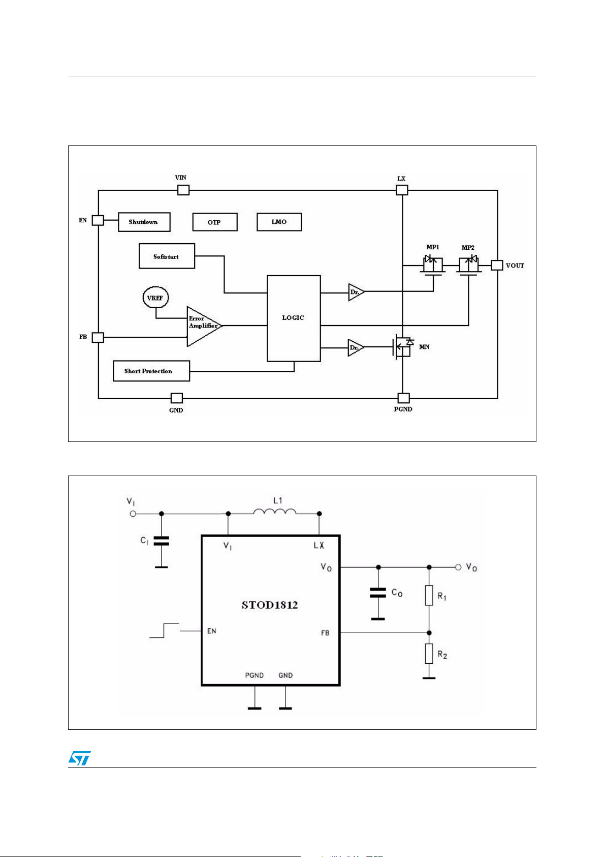
Figure 1. Internal block diagram
Figure 2. Schematic diagram
3/19
Page 4

Pin configuration STOD1812
2 Pin configuration
Figure 3. Pin connections (top view)
Table 2. Pin description
Pin n° Symbol Description
1 OUT Output voltage
2 OUT Output voltage
3 GND Ground
4 FB Feedback
5EN
6V
7L
8L
I
X
X
DC supply voltage enable control pin. ON =V
shutdown mode.
Input supply voltage.
Switching node
Switching node
9 PGND Power ground
10 PGND Power ground
Exp Pad Exposed Pad. It must be connected to power ground
. When pulled low put the device in
I
4/19
Page 5

STOD1812 Maximum ratings
3 Maximum ratings
Table 3. Absolute maximum ratings
Symbol Parameter Value Unit
V
I
DC supply voltage -0.3 to 6 V
EN Enable pin -0.3 to 6 V
FB Feedback pin -0.3 to 6 V
Switching node -0.3 to 20 V
Switching current Internally limited A
Converter output voltage -0.3 to 20 V
Power dissipation Internally limited mW
Storage temperature range -65 to 150 °C
Operating temperature range -40 to 125 °C
V
T
L
I
LX
OUT
P
STG
T
X
D
J
Table 4. Thermal data
Symbol Parameter Value Unit
R
thJA
Thermal resistance junction-ambient (tested on 2 layers board) 30.9 °C/W
Table 5. ESD data
Symbol Parameter Value Unit
ESD Human Body Model 2 kV
5/19
Page 6

Electrical characteristics STOD1812
4 Electrical characteristics
Table 6. Electrical characteristics
(T
= -40 °C to 125 °C, VI = 3.6 V, CI = CO = 4.7 µF, L = 2.2 µH, IO = 80 mA, V
J
V
= 18 V, R1=270 kΩ, R2 = 20 kΩ unless otherwise specified).
O
Symbol Parameter Test conditions Min. Typ. Max. Unit
Supply section
EN
= VI,
V
I
O
UVLO_H
UVLO_L
Supply input voltage IO=0 to 120mA 2.5 5.5 V
I
Load current VI=2.5V to 5.5V 120 mA
Under voltage lockout
HIGH
Under voltage lockout
LOW
2.1 2.2 V
=120mA 1.3 mA
I
O
2.3 2.4 V
No Load, Switching 0.3 mA
I
Q
V
EN
V
EN
I
EN
Quiescent current
VFB=VI - No Load, No Switching 35 50 µA
=GND 100 300 nA
V
EN
H Enable high threshold VI=2.5V to 5.5V 1.2 V
L Enable low threshold VI=2.5V to 5.5V 0.4 V
Enable input current VEN=Vi 500 nA
Dynamic performance
T
ON MAXTON
T
SS
D
MAX
ν Efficiency
max time 0.5 µs
Soft-start time From enable to output regulation 0.6 ms
Maximum duty cycle 95 %
I
=5 to 30mA 75 %
O
=30 to 120mA 85 %
I
O
Step-up converter section
ΔV
ΔV
6/19
V
I
V
O_MAX
ΔV
O_SLO
ΔV
O_LOT
FB1
FB
O_SLI
O_LIT
Feedback voltage VI=2.5V to 5.5V 1.18 1.21 1.24 V
Feedback leakage
current
=2.5V to 5.5V 30 100 nA
V
I
Output voltage range VI=2.5V to 5.5V; IO=0 to 120mA 18 V
Static line regulation VI=2.5V to 5.5V, IO1=120mA, 0.6 %/V
Static load regulation IO=0 to 120mA, VI=3.6V; 0.0016 %/mA
Line transient
regulation
Load transient
regulation
VI=2.5V to 3.0V, IO1=120mA,
=50µs TA=25°C
T
R=TF
IO=5 to 120mA and IO=120 to 5mA,
TR=TF=10µs TA=25°C, peak to peak
80 mV
250 mV
Page 7

STOD1812 Electrical characteristics
Table 6. Electrical characteristics (continued)
(T
= -40 °C to 125 °C, VI = 3.6 V, CI = CO = 4.7 µF, L = 2.2 µH, IO = 80 mA, V
J
V
= 18 V, R1=270 kΩ, R2 = 20 kΩ unless otherwise specified).
O
Symbol Parameter Test conditions Min. Typ. Max. Unit
=5 to 120mA at 200Hz-Pulse
I
O
TDMA noise standard,
0.5V
PP
TA=25°C see Figure 14
40 mV
0.60 0.80 Ω
0.25 0.65 Ω
R
R
DSON
SVR
I
PK
DSON
Supply voltage
rejection
Inductor peak current TA=25°C 2.4 A
Resistance on
P
P-channel
Resistance on
N
N-channel
Thermal shutdown
EN
= VI,
OTP
OTP
Over temperature
protection
Over temperature
HYST
protection hysteresis
150 °C
20 °C
7/19
Page 8

Functional description STOD1812
5 Functional description
5.1 Boost controller
STOD1812 is a boost converter operating in PFM (pulsed frequency modulation) mode. The
converter monitors the output voltage through the bridge resistor divider R
when the feedback voltage falls below the feedback voltage, the boost switch t
and the inductor current ramps up. The inductor current is measured by detecting the
temperature compensated drain voltage of the boost MOSFET. The boost turns off when its
drain voltage reaches the internal reference, the main switch remains off until the minimum
off time has passed and the feedback voltage is below the reference again. A maximum ON
time prevents the switch t
In order to calculate the values of the bridge resistors with a fixed V
from staying ON for an excessively long period.
SW
O
can be used:
R
V
V
O
O
1,21
1,21
-1 =
-1 =
R
1
1
R
R
2
2
and R2, and
1
turns on
SW
, the following formula
5.2 Enable
The ENABLE pin is a logic input signal that turns on the controller when the voltage on this
pin is equal to or higher than 1.2 V. When the voltage is at or below 0.4 V the STOD1812
goes into shutdown mode. In this case, the true-shutdown switch is turned off and the
overall power consumption is reduced to 0.1 µA. No pull-up or pull-down is present on this
pin.
5.3 Efficiency
The total consumption of some PMOLED displays can be as low as 1 mA. In order to
increase the battery life of the device, the STOD1812 offers high efficiency over a wide
range of output load current and input voltages. See typical application efficiency
performance in Section 8 on page 11.
5.4 Under voltage lockout (UVLO)
The minimum supply voltage is 2.5 V, under which the undervoltage lockout circuit operates
with a typical threshold of 2.3 V.
8/19
Page 9

STOD1812 Typical application information
6 Typical application information
Figure 4. Typical application circuit connections
Table 7. External components
Symbol Parameter Min. Typ. Max. Unit
L Inductor (I
C
C
Ceramic capacitor SMD 4.7 µF
I
Ceramic capacitor SMD 4.7 µF
O
R1 Feedback resistor (for V
R2 Feedback resistor (for V
= 2.5 A) 2.2 µH
SAT
= 18 V) 270 kΩ
O
= 18 V) 20 kΩ
O
Note: The external components suggested in this document should be considered as a design
reference guide. The performance data mentioned in the electrical characteristics table are
not guaranteed for all the possible electrical parameters of the components included in this
list. However, the operation of STOD1812 is not limited to the use of components included in
this list.
9/19
Page 10

Demonstration board STOD1812
7 Demonstration board
Figure 5. Demonstration board photo
Figure 6. Suggested demonstration board schematic (top layer view)
Figure 7. Suggested demonstration board schematic (bottom layer view)
10/19
Page 11

STOD1812 Typical application performance
O
O
8 Typical application performance
(VO = 18 V, L = 2.2 µH, CI = CO = 4.7 µF, R1 = 270 kΩ, R2 = 20 kΩ)
Figure 8. Efficiency vs output current Figure 9. Efficiency vs input voltage
100
100
100
Efficiency [%]
Efficiency [%]
Figure 10. Efficiency vs temperature Figure 11. Frequency vs temperature
VI = V
= 3.6 V, IO = from 5 mA to 120 mA, T = 25°C
VI = V
= 3.6 V, IO = from 5 mA to 120 mA, T = 25°C
EN
90
90
80
80
70
70
60
60
50
50
40
40
0 20 40 60 80 100 120
0 20 40 60 80 100 120
EN
[mA]
[mA]
I
I
100
VI = V
= from 2.5 V to 5.5 V, IO = 120 mA, T = 25 °C
VI = V
= from 2.5 V to 5.5 V, IO = 120 mA, T = 25 °C
EN
90
90
80
80
70
70
60
60
Efficiency [%]
Efficiency [%]
50
50
40
40
2.533.544.555.5
2.533.544.555.5
EN
[V]
[V]
V
V
I
I
2.5
100
100
90
90
80
80
70
70
60
60
Efficiency [%]
Efficiency [%]
50
50
40
40
-75 -50 -25 0 25 50 75 100 125 150 175
-75 -50 -25 0 25 50 75 100 125 150 175
Figure 12. Line transient Figure 13. Load transient response
VI = V
= 3.6 V, IO = 120 mA
VI = V
= 3.6 V, IO = 120 mA
EN
EN
T [°C]
T [°C]
2.5
2.3
2.3
2.1
2.1
1.9
1.9
1.7
1.7
1.5
1.5
1.3
1.3
1.1
1.1
Frequency [MHz]
Frequency [MHz]
0.9
0.9
0.7
0.7
0.5
0.5
I
O
V
O
V
= V
= 3.6 V, IO = 80 mA
V
= V
= 3.6 V, IO = 80 mA
IN
EN
IN
EN
-75 -50 -25 0 25 50 75 100 125 150 175
-75 -50 -25 0 25 50 75 100 125 150 175
T [°C]
T [°C]
VI = from 2.5 V to 3 V, IO = 120 mA, VI (t
T = 25 °C
RISE
= t
FALL
) = 50µs,
VI = 3.6 V, IO from 5mA to 120mA, t
T = 25 °C
RISE
= t
FALL
= 10 µs,
11/19
Page 12

Typical application performance STOD1812
Figure 14. TDMA noise
VI=V
INH
V
O
VI = V
= from 2.9 V to 3.4 V, IO = 120 mA,
INH
VI (t
) = 50 µs, T = 25 °C
RISE
12/19
Page 13

STOD1812 Package mechanical data
9 Package mechanical data
In order to meet environmental requirements, ST offers these devices in ECOPACK®
packages. These packages have a lead-free second level interconnect. The category of
second Level Interconnect is marked on the package and on the inner box label, in
compliance with JEDEC Standard JESD97. The maximum ratings related to soldering
conditions are also marked on the inner box label. ECOPACK is an ST trademark.
ECOPACK specifications are available at: www.st.com.
13/19
Page 14

Package mechanical data STOD1812
Figure 15. DFN10L package outline
14/19
8049731/A
Page 15

STOD1812 Package mechanical data
Table 8. DFN10L mechanical data
mm. inch.
Dim.
Min. Typ. Max. Min. Typ. Max.
A 0.70 0.75 0.80 0.028 0.030 0.031
A1 0 0.02 0.05 0 0.001 0.002
A3 0.20 0.008
b 0.18 0.25 0.30 0.007 0.010 0.012
D 2.90 3 3.10 0.114 0.118 0.122
D2 2.23 2.38 2.48 0.088 0.094 0.098
E 2.90 3 3.10 0.114 0.118 0.122
E2 1.49 1.64 1.74 0.059 0.065 0.069
e 0.50 0.020
L 0.30 0.40 0.50 0.012 0.016 0.020
15/19
Page 16

Package mechanical data STOD1812
Tape & reel QFNxx/DFNxx (3x3) mechanical data
mm. inch.
Dim.
Min. Typ. Max. Min. Typ. Max.
A180 7.087
C 12.8 13.2 0.504 0.519
D 20.2 0.795
N60 2.362
T 14.4 0.567
Ao 3.3 0.130
Bo 3.3 0.130
Ko 1.1 0.043
Po 4 0.157
P 8 0.315
16/19
Page 17

STOD1812 Package mechanical data
Figure 16. DFN10L footprint - recommended data
17/19
Page 18

Revision history STOD1812
10 Revision history
Table 9. Document revision history
Date Revision Changes
25-Mar-2008 1 Initial release.
18/19
Page 19

STOD1812
Please Read Carefully:
Information in this document is provided solely in connection with ST products. STMicroelectronics NV and its subsidiaries (“ST”) reserve the
right to make changes, corrections, modifications or improvements, to this document, and the products and services described herein at any
time, without notice.
All ST products are sold pursuant to ST’s terms and conditions of sale.
Purchasers are solely responsible for the choice, selection and use of the ST products and services described herein, and ST assumes no
liability whatsoever relating to the choice, selection or use of the ST products and services described herein.
No license, express or implied, by estoppel or otherwise, to any intellectual property rights is granted under this document. If any part of this
document refers to any third party products or services it shall not be deemed a license grant by ST for the use of such third party products
or services, or any intellectual property contained therein or considered as a warranty covering the use in any manner whatsoever of such
third party products or services or any intellectual property contained therein.
UNLESS OTHERWISE SET FORTH IN ST’S TERMS AND CONDITIONS OF SALE ST DISCLAIMS ANY EXPRESS OR IMPLIED
WARRANTY WITH RESPECT TO THE USE AND/OR SALE OF ST PRODUCTS INCLUDING WITHOUT LIMITATION IMPLIED
WARRANTIES OF MERCHANTABILITY, FITNESS FOR A PARTICULAR PURPOSE (AND THEIR EQUIVALENTS UNDER THE LAWS
OF ANY JURISDICTION), OR INFRINGEMENT OF ANY PATENT, COPYRIGHT OR OTHER INTELLECTUAL PROPERTY RIGHT.
UNLESS EXPRESSLY APPROVED IN WRITING BY AN AUTHORIZED ST REPRESENTATIVE, ST PRODUCTS ARE NOT
RECOMMENDED, AUTHORIZED OR WARRANTED FOR USE IN MILITARY, AIR CRAFT, SPACE, LIFE SAVING, OR LIFE SUSTAINING
APPLICATIONS, NOR IN PRODUCTS OR SYSTEMS WHERE FAILURE OR MALFUNCTION MAY RESULT IN PERSONAL INJURY,
DEATH, OR SEVERE PROPERTY OR ENVIRONMENTAL DAMAGE. ST PRODUCTS WHICH ARE NOT SPECIFIED AS "AUTOMOTIVE
GRADE" MAY ONLY BE USED IN AUTOMOTIVE APPLICATIONS AT USER’S OWN RISK.
Resale of ST products with provisions different from the statements and/or technical features set forth in this document shall immediately void
any warranty granted by ST for the ST product or service described herein and shall not create or extend in any manner whatsoever, any
liability of ST.
ST and the ST logo are trademarks or registered trademarks of ST in various countries.
Information in this document supersedes and replaces all information previously supplied.
The ST logo is a registered trademark of STMicroelectronics. All other names are the property of their respective owners.
© 2008 STMicroelectronics - All rights reserved
STMicroelectronics group of companies
Australia - Belgium - Brazil - Canada - China - Czech Republic - Finland - France - Germany - Hong Kong - India - Israel - Italy - Japan -
Malaysia - Malta - Morocco - Singapore - Spain - Sweden - Switzerland - United Kingdom - United States of America
www.st.com
19/19
 Loading...