

STGB7NB40LZ
N-CHANNEL CLAMPED 14A - D2PAK
INTERNALLY CLAMPED PowerMESH™ IGBT
TYPE V
CES
V
CE(sat)
I
C
STGB7NB40LZ CLAMPED < 1.50 V14A
■ POLYSILICON GATE VOLTAGE DRIVEN
■ LOW THRESHOLD VOLTAGE
■ LOW ON-VOLTAGE DROP
■ LOW GATE CHARGE
■ HIGH CURRENT CAPABILITY
■ HIGH VOLTAGE CLAMPING FEATURE
DESCRIPTION
Using thelatest highvoltage t echnology based on a
patented strip layout, STMicroelectronics has
designed an advanced family of IG BTs, the
PowerMESH
™
IGBTs, with outstanding
performances. The built in collector-gate zener
exhibits a very precise active clamping while the
gate-emitter zener supplies an ESD protection.
APPLICATIONS
■ AUTOMOTIVE IGNITION
3
1
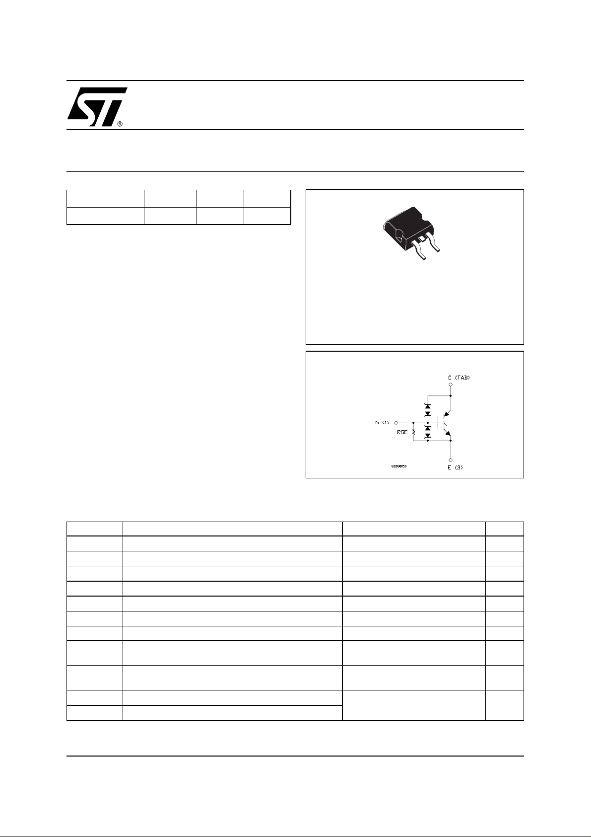
D2PAK
INTERNAL SCHEMATIC DIAGRAM
ABSOLUTE MAXIMUM RATINGS
Symbol Parameter Value Unit
V
V
V
P
E
CES
ECR
GE
I
C
R
G
TOT
E
CL
ECAV
T
stg
T
j
Collector-Emitter Voltage (VGS=0)
CLAMPED V
Reverse Battery Protection 20 V
Gate-Emitter Voltage CLAMPED V
Collector Current (continuous) at 100°C 14 A
Minimum External Gate Resistor 500 Ω
Total Dissipation at TC= 25°C
100 W
Derating Factor 0.66 W/°C
Single Pulse Collector to Emitter Avalanche Energy
=13A;Tj= 150°C (see fig.1-2)
I
C
Reverse Avalanche Energy
= 7 A ;f= 100 Hz ; Tc= 25°C
I
C
Storage Temperature
Operating Junction Temperature
130 mJ
10 mJ
–55 to 175 °C
1/8March 2003
STGB7NB40LZ
THERMAL DATA
Rthj-case Thermal Resistance Junction-case Max 1.5 °C/W
Rthj-amb Thermal Resistance Junction-ambient Max (free air) 62.5 °C/W
ELECTRICAL CHARACTERISTICS (T
= 25°C UNLESS OTHERWISE SPECIFIED)
CASE
OFF
Symbol Parameter Test Conditions Min. Typ. Max. Unit
BV
BV
(CES)
(ECS)
Collector-Emitter Clamped
Voltage
Emitter Collector Break-down
IC=10mA,VGE=0,
370 400 430 V
Tc= - 40°C to 150°C; RG=1KΩ
IEC= 75 mA, VGE=0, 20 27 V
Voltage
BV
GE
Gate Emitter Break-down
IG=±2mA 12 16 V
Voltage
I
CES
I
GES
Collector-Emitter Leakage
Current
Gate-Emitter Leakage
Current (V
CE
=0)
VGE=200V,VGE=0,RG=1KΩ
Tc=25°C
Tc=150°C
V
=±10V,VCE= 0 1000 µA
GE
25
250
ON (1)
Symbol Parameter Test Conditions Min. Typ. Max. Unit
V
GE(th)
V
CE(SAT)
R
GE
Gate Threshold Voltage VCE=VGE,IC= 1 mA, Tc=25°C
= 1 mA, Tc=150°C
Collector-Emitter Saturation
Voltage
V
CE=VGE,IC
VGE=4.5 V, IC=7A,Tj=25°C
V
=5.0 V, IC=14A,Tc=25°C
GE
Gate Emitter Resistance
1.2
0.75
1.3 1.50
10 20
2.2
1.8
1.9
30
DYNAMIC
Symbol Parameter Test Conditions Min. Typ. Max. Unit
V
C
ies
C
oes
C
res
Input Capacitance
Output Capacitance 80 pF
Reverse Transfer
Capacitance
Q
g
Gate Charge VCE=40V,IC=7A,
=25V,f=1MHz,VGE=0
CE
V
=5V
GE
910 pF
15 pF
22 nC
µA
µA
V
V
V
V
KΩ
SWITCHING ON
Symbol Parameter Test Conditions Min. Typ. Max. Unit
=14V,RG=1KΩ,
V
CE
RL=1Ω, VGE=5 V
VCE= 300 V, RG=1KΩ ,
R
=46Ω, VGE=5 V
L
0.9
4.5
4.4
3.6
2/8
t
d(on)
t
d(off)
Delay Time
t
r
Current Rise Time
Delay Time
t
f
Current Fall Time
µs
µs
µs
µs
Thermal Imped ance
STGB7NB40LZ
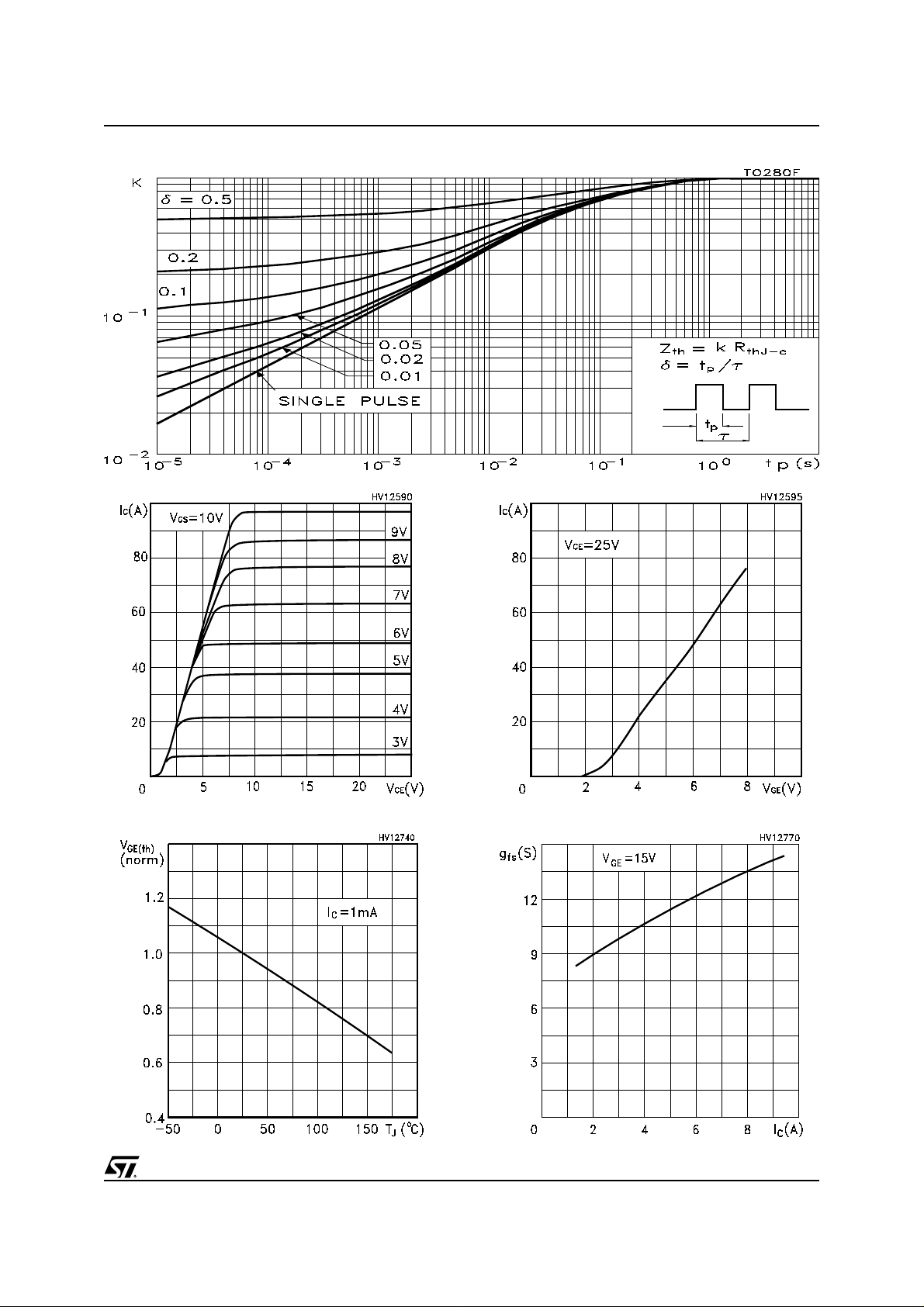
Output Characteristics
Normalized Gate Threshold Voltage vs Temp. Transconductance
Transfer Characteristics
3/8

STGB7NB40LZ
Normalized Collector-Emitter On Voltage vs
Temperature
Capacitance Variations
Collector-Emitter On Voltage vs Gate-Emitter
Voltage
Gate-Charge vs Gate-Emitter Voltage
Normalized Break-dow n Voltage vs Temp. Clamping Voltage vs Gate Resistance
4/8

And Diode Recovery Times
STGB7NB40LZ
Fig. 2: Unclamped Inductive WaveformFig. 1: Unclamped Inductive Load Test Circuit
Fig. 4: Gate Charge test CircuitFig. 3: Test Circuit For Inductiv e Load Switching
5/8

STGB7NB40LZ
D2PAK MECHANICAL DATA
DIM.
MIN. TYP MAX. MIN. TYP. MAX.
A 4.4 4.6 0.173 0.181
A1 2.49 2.69 0.098 0.106
A2 0.03 0.23 0.001 0.009
B 0.7 0.93 0.027 0.036
B2 1.14 1.7 0.044 0.067
C 0.45 0.6 0.017 0.023
C2 1.23 1.36 0.048 0.053
D 8.95 9.35 0.352 0.368
D1 8 0.315
E 10 10.4 0.393
E1 8.5 0.334
G 4.88 5.28 0.192 0.208
L 15 15.85 0.590 0.625
L2 1.27 1.4 0.050 0.055
L3 1.4 1.75 0.055 0.068
mm. inch
M 2.4 3.2 0.094 0.126
R 0.4 0.015
V2 0º 8º
3
6/8
1

STGB7NB40LZ
D2PAK FOOTPRINT
TAPE AND REEL SHIPMENT (suffix ”T4”)*
TUBE SHIPMENT (no suffix)*
REEL MECHANICAL DATA
DIM.
A 330 12.992
B 1.5 0.059
C 12.8 13.2 0.504 0.520
D 20.2 07 95
G 24.4 26.4 0.960 1.039
N 100 3.937
T 30.4 1.197
mm inch
MIN. MAX. MIN. MAX.
TAPE MECHANICAL DATA
DIM.
A0 10.5 10.7 0.413 0.421
B0 15.7 15.9 0.618 0.626
D 1.5 1.6 0.059 0.063
D1 1.59 1.61 0.062 0.063
E 1.65 1.85 0.065 0.073
F 11.4 11.6 0.449 0.456
K0 4.8 5.0 0.189 0.197
P0 3.9 4.1 0.153 0.161
P1 11.9 12.1 0.468 0.476
P2 1.9 2.1 0.075 0.082
R 50 1.574
T 0. 25 0.35 0.0098 0.0137
W 23.7 24.3 0.933 0.956
* on sales ty pe
mm inch
MIN. MAX. MIN. MAX.
BASE QTY BULK QTY
1000 1000
7/8

STGB7NB40LZ
Information furnished is believed to be accurate and reliable. However, STMicroelectronics assumes no responsibility for the
consequences of u se of such inf ormat ion nor for any in fring ement of p aten ts or othe r ri ghts of th ird p arties whic h may resul t f rom
its use. No license is granted by implication or otherwise under any patent or patent rights of STMicroelectronics. Specifications
mentioned in this publication are subject to change without notice. This publication supersedes and replaces all information
previously supplied. STMicroelectronics products are not authorized for use as critical components in life support devices or
systems without express written approval of STMicroelectronics.
Australia - Brazil - Canada - China - Finland - France - Germany - Hong Kong - India - Israel - Italy - Japan - Malaysia - Malta - Morocco
© The ST logo is a registered trademark of STMicroelectronics
© 2003 STMicroelectronics - Printed in Italy - All Rights Reserved
Singapore - Spain - Sweden - Switzerland - United Kingdom - United States.
STMicroelectronics GROUP OF COMPANIES
© http://www.st.com
8/8
 Loading...