

Page 1

Low voltage 0.5 Ω single SPDT switch with
break-before-make feature and 15 kV contact ESD protection
Features
■ Wide operating voltage range:
V
(opr) = 1.65 to 4.8 V
CC
■ Low power dissipation:
I
= 0.2 µA (max.) at TA = 85 °C
CC
■ Low "ON" resistance:
–R
–R
–R
■ Separate supply voltage for switch and control
pins
■ Latch-up performance exceeds 100mA per
JESD 78, Class II
■ ESD performance tested on common pin
(D pin):
– 15 kV IEC-61000-4-2 ESD, contact
– 8 kV HBM JESD22 A114-B Class II
■ ESD performance tested on S1 and S2 pin:
– 8 kV IEC-61000-4-2 ESD, contact
■ ESD performance test on all other pins:
– 4 kV HBM (JESD22 A114-B Class II)
– 400 V machine model (JESD22 A115-A)
– 1500 V charged-device model
Applications
■ Mobile phones
Table 1. Device summary
= 0.75 Ω (TA = 25 ºC)
ON
at V
at V
at V
= 2.25 V
CC
= 0.50 Ω (TA = 25 ºC)
ON
= 3.0 V
CC
=0.40Ω (TA =25ºC)
ON
=4.3V
CC
discharge
discharge
(JESD22 C101)
STG4160
Flip-chip 8
Description
The STG4160 is a high-speed CMOS low voltage
single analog SPDT (single pole dual throw)
switch or 2:1 multiplexer/demultiplexer switch
fabricated in silicon gate C
designed to operate from 1.65 to 4.8 V, making
this device ideal for portable applications. It offers
low ON resistance (0.40 Ω typ.) at V
The SEL inputs are provided to control the
switches.
The switch S1 is ON (connected to common port
D) when the SEL input is held high and OFF (high
impedance state exists between the two ports)
when SEL is held low. The switch S2 is ON
(connected to common Port D) when the SEL
input is held low and OFF (high impedance state
exist between the two ports) when SEL is held
high.
Additional key features are fast switching speed,
break-before-make delay time and ultra power
consumption. All inputs and outputs are equipped
with protection circuits against static discharge,
giving them ESD immunity and transient excess
voltage.
2
MOS technology. It is
= 4.3 V.
CC
Order code Package Packing
STG4160BJR Flip-chip 8 Tape and reel
February 2009 Rev 2 1/19
www.st.com
19
Page 2

Contents STG4160
Contents
1 Pin settings . . . . . . . . . . . . . . . . . . . . . . . . . . . . . . . . . . . . . . . . . . . . . . . . 3
1.1 Pin connections . . . . . . . . . . . . . . . . . . . . . . . . . . . . . . . . . . . . . . . . . . . . . 3
1.2 Pin description . . . . . . . . . . . . . . . . . . . . . . . . . . . . . . . . . . . . . . . . . . . . . . 3
2 Logic diagram . . . . . . . . . . . . . . . . . . . . . . . . . . . . . . . . . . . . . . . . . . . . . . 4
3 Maximum ratings . . . . . . . . . . . . . . . . . . . . . . . . . . . . . . . . . . . . . . . . . . . . 5
4 Electrical characteristics . . . . . . . . . . . . . . . . . . . . . . . . . . . . . . . . . . . . . 6
5 Test circuits . . . . . . . . . . . . . . . . . . . . . . . . . . . . . . . . . . . . . . . . . . . . . . . 10
6 Package mechanical data . . . . . . . . . . . . . . . . . . . . . . . . . . . . . . . . . . . . 14
7 Revision history . . . . . . . . . . . . . . . . . . . . . . . . . . . . . . . . . . . . . . . . . . . 16
2/19
Page 3

STG4160 Pin settings
1 Pin settings
1.1 Pin connections
Figure 1. STG4160 pin connections
VL
S2
GND
S1
1.2 Pin description
Table 2. Pin assignment
Pin number Symbol Name and function
1 S1 Independent channel
2 GND Ground (0 V)
3 S2 Independent channel
4V
5V
6 SEL Control
7 D Common channel
Bump View Top View
45
3 6
2
7
8
1
VCC
SEL
D
GND
S1
GND
S2
VL
L
CC
8
1
7
2
6
3
4
5
Logic supply voltage
Positive supply voltage
D
SEL
V
CS00028
8 GND Ground (0 V)
3/19
Page 4

Logic diagram STG4160
2 Logic diagram
Figure 2. Functional diagram
D
Figure 3. Circuit equivalent logic
S1
S2
SEL
S2
S1
Table 3. Truth table
SEL Switch S1 Switch S2
HON
L
1. High impedance
4/19
OFF
(1)
OFF
ON
(1)
Page 5

STG4160 Maximum ratings
3 Maximum ratings
Stressing the device above the rating listed in the “Absolute maximum ratings” table may
cause permanent damage to the device. These are stress ratings only and operation of the
device at these or any other conditions above those indicated in the Operating sections of
this specification is not implied. Exposure to Absolute maximum rating conditions for
extended periods may affect device reliability. Refer also to the STMicroelectronics SURE
Program and other relevant quality documents.
Table 4. Absolute maximum ratings
Symbol Parameter Value Unit
V
CC
V
V
V
V
I
IKC
I
IK
I
OK
I
O
I
OP
I
or I
CC
P
T
stg
T
1. Derate above 70 ºC by 18.5 mW/C
Table 5. Recommended operating conditions
Supply voltage -0.5 to 5.5 V
Logic supply voltage -0.5 to 5.5 V
L
DC input voltage -0.5 to VCC +0.5 V
I
DC control input voltage -0.5 to VL +5.5 V
IC
DC output voltage -0.5 to VCC +0.5 V
O
DC input diode current on control pin (V
DC input diode current (V
<0V) ±50 mA
SEL
<0V) -50 mA
SEL
DC output diode current ± 20 mA
DC output current ± 300 mA
DC output current peak (pulse at 1ms, 10% duty cycle) ± 500 mA
DC VCC or ground current ± 100 mA
GND
Power dissipation at TA= 70ºC
D
(1)
500 mW
Storage temperature -65 to 150 °C
Lead temperature (10 sec) 260 °C
L
Symbol Parameter Value Unit
V
V
V
V
V
T
dt/dv
1. VL pin should not be left floating.
Supply voltage 1.65 to 4.8 V
CC
Logic supply voltage
L
Input voltage 0 to V
I
Control input voltage 0 to V
IC
Output voltage 0 to V
O
Operating temperature -40 to 85 °C
op
Input rise and fall time control
input
(1)
1.65 to V
= 1.65 to 2.7 V 0 to 20
V
L
= 3.0 to 4.8 V 0 to 10
V
L
CC
CC
L
CC
V
V
V
V
ns/V
5/19
Page 6
Electrical characteristics STG4160
4 Electrical characteristics
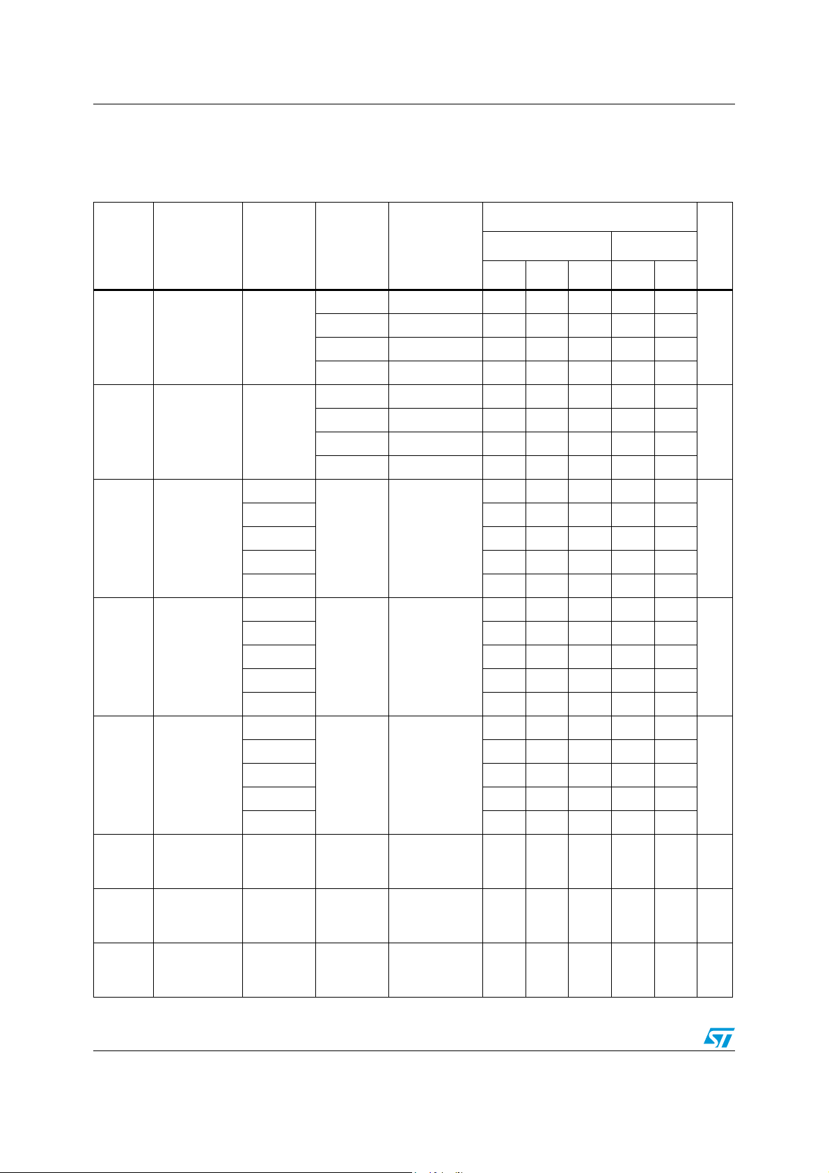
Table 6. DC specifications
Symbol Parameter
V
IH
V
IL
High level
input voltage
Low level
input voltage
V
CC
(V)
1.65 – 4.3
1.65 – 4.3
1.8
2.25 0.75 1.0 1.3
ON
ON resistance
R
3 0.50 0.65 0.8
3.7 0.45 0.55 0.7
4.3 0.40 0.5 0.65
1.8
2.25 20
310
3.7 10
ΔR
ON resistance
match
ON
between
channels
(1)
4.3 10
Val ue
V
(V)
L
Test condition
= 25 °C -40 to 85 °C
A
Min Typ Max Min Max
1.65 – 1.95 1.25 1.25
2.3 – 2.7 1.75 1.75
3.0 – 3.6 2.34 2.34
4.3 2.80 2.80
1.65 – 1.95 0.6 0.6
2.3 – 2.7 0.8 0.8
3.0 – 3.6 1.05 1.05
4.3 1.5 1.5
1.5 2.5 3.7
=0V to
V
S
1.65 – 4.3
V
CC
IS=100mA
40
=0V to
V
S
1.65 – 4.3
V
CC
IS=100mA
UnitT
V
V
Ω
mΩ
1.8
R
FLAT
ON resistance
flatness
(2)
2.25 300 430 550
3 150 190 270
1.65 – 4.3
3.7 140 180 230
VS=0V to
V
CC
IS=100mA
4.3 140 180 220
I
OFF
I
ON
I
D
Sn OFF state
leakage
current
Sn ON state
leakage
current
D ON state
leakage
current
4.3 4.3
4.3 4.3
4.3 4.3
VS= 0.3 to 4.0
V
D
VS= 0.3 to 4.0
V
D
VS= open
V
D
6/19
= 0.3 to 4.0
= open
= 0 to 4.0
1.0 1.7 2.0
mΩ
-30 30 -300 300 nA
-30 30 -300 300 nA
-30 30 -300 300 nA
Page 7
STG4160 Electrical characteristics
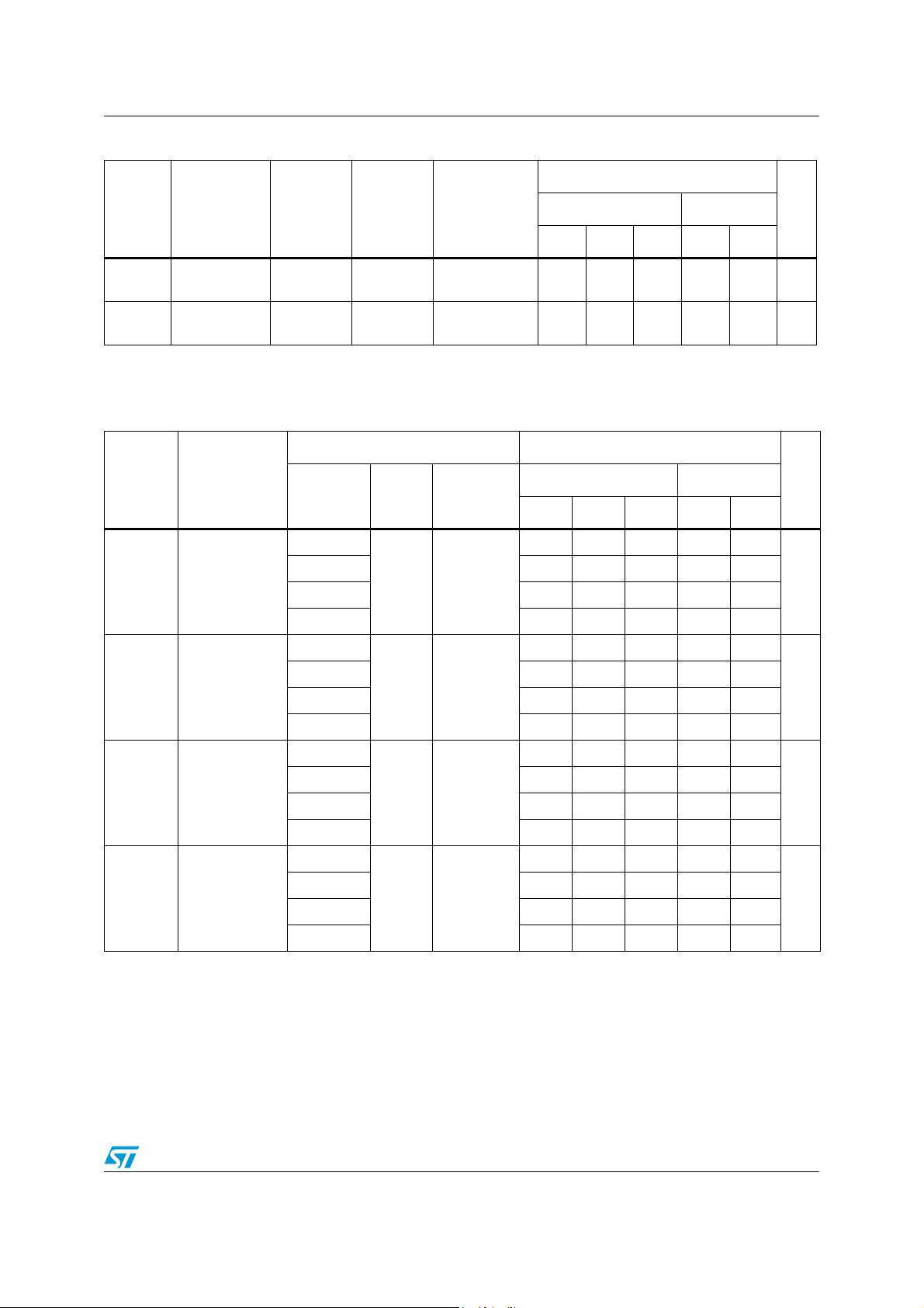
Table 6. DC specifications (continued)
Val ue
Symbol Parameter
V
CC
(V)
V
(V)
L
Test condition
= 25 °C -40 to 85 °C
A
Min Typ Max Min Max
UnitT
CC
Quiescent
supply current
SEL leakage
current
- R
ON(Max)
ON(Min)
1.65 – 4.3 1.65 – 4.3
1.65 – 4.3 1.65 – 4.3
I
I
SEL
1. ΔRON = R
2. Flatness is defined as the difference between the maximum and minimum value of on-resistance as measured over the specified analog
signal ranges.
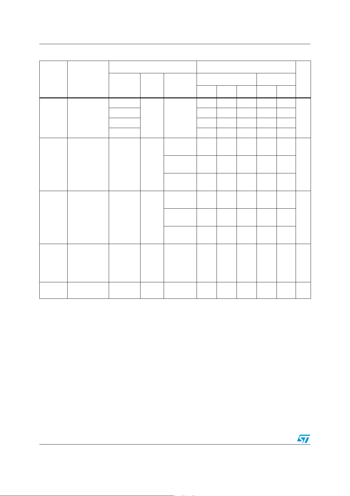
Table 7. AC electrical characteristics (CL = 35 pF, RL = 50 Ω, tr = tf ≤5ns)
V
SEL=VCC
GND
V
SEL
GND
or
=4.3V or
-0.05 0.05 -0.2 0.2 μA
-0.2 0.2 -2 2 μA
Test conditions Value
Symbol Parameter
, t
PHL
Propagation
delay
t
PLH
V
(V)
CC
V
(V)
L
1.65 – 1.95
2.3 – 2.7 0.14
3.0 – 3.3 0.12
1.65 –
4.3
T
= 25°C -40 to 85°C
A
Min Typ Max Min Max
0.18
3.6 – 4.3 0.12
t
ON
TURN-ON time
1.65 – 1.95
= V
V
S
2.3 – 2.7 48 62 80
3–3.6 33 43 56
1.65 –
4.3
CC
RL = 50 Ω
CL = 30 pF
70 123 160
4.3 29 38 49
36 45 60
t
OFF
TURN-OFF
time
1.65 – 1.95
= V
V
S
2.3 – 2.7 35 47 62
3–3.6 30 40 51
1.65 –
4.3
CC
RL = 50 Ω
= 30 pF
C
L
4.3 29 38 50
1.65 – 1.95
= 35 pF
4.3
C
L
R
L
V
S
= 50 Ω
= VCC/2
Break-before-
t
D
make time
delay
2.3 – 2.7 10 22
1.65 –
3 – 3.6 5 15
10 42
4.3 5 12
Unit
ns
ns
ns
ns
7/19
Page 8
Electrical characteristics STG4160
Table 7. AC electrical characteristics (CL = 35 pF, RL = 50 Ω, tr = tf ≤5 ns) (continued)
Test conditions Value
Symbol Parameter
V
(V)
CC
V
(V)
L
1.65 – 1.95
Q
Charge
injection
2.3–2.7 98
1.65 –
3.0 – 3.3 133
4.3
C
V
= 1 nF
L
GEN
= 0 V
3.6 – 4.3 162
= 1 V
V
S
RMS
f = 100 kHz
V
= 1V
S
S
= 1V
RMS
RMS
OIRR
Off isolation
(1)
1.65 – 4.3 4.3
f = 1 MHz
V
f = 5 MHz
= 1V
V
S
RMS
f = 100 kHz
V
= 1V
S
S
= 1V
RMS
RMS
Xtalk Crosstalk 1.65 – 4.3 4.3
f = 1 MHz
V
f = 5 MHz
= 600 Ω
R
L
= 50 pF
C
THD
Total harmonic
distortion
2.3–4.3 4.3
L
VS = V
CC
f = 600 Hz
to 20 kHz
BW
1. OFF-isolation = 20 log10 (VD/VS), VD = output, VS = input to off switch
-3dB Bandwidth
(switch ON)
1.65 – 4.3 4.3 R
= 50 Ω 50 MHz
L
TA = 25°C -40 to 85°C
Min Typ Max Min Max
75
77
67
50
80
67
50
0.01 %
Unit
pC
dB
dB
8/19
Page 9
STG4160 Electrical characteristics
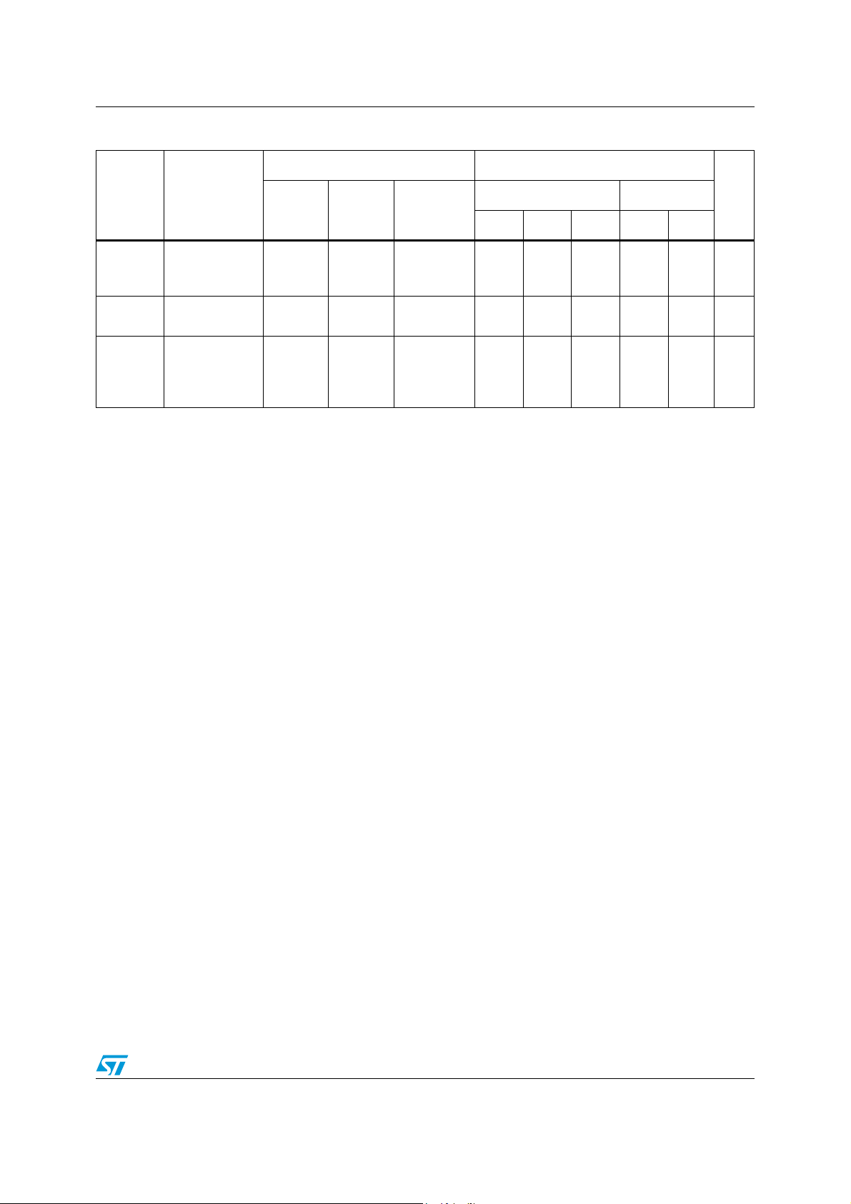
Table 8. Capacitive characteristics
Test condition Value
Symbol Parameter
V
CC
(V)
Control pin
C
SEL
input
1.8 –4.3 1.8–4.3 VL=V
capacitance
SN
Sn port
capacitance
1.8–4.3 1.8–4.3 V
C
D port
C
capacitance
D
when the switch
1.8– 4.3 1.8–4.3 V
is enabled
V
(V)
T
= 25 °C -40 to 85 °C
L
A
Unit
Min Typ Max Min Max
CC
L=VCC
L=VCC
30 pf
94 pf
227 pf
9/19
Page 10
Test circuits STG4160
5 Test circuits
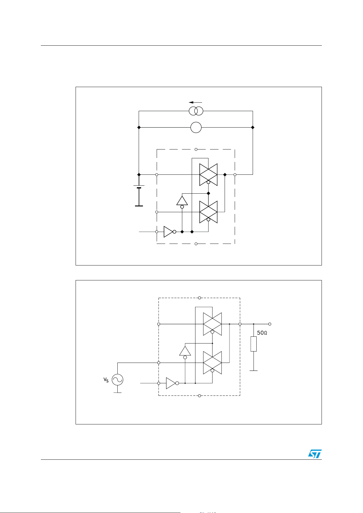
Figure 4. ON resistance
I
DS
V
V
CC
VS
GND
Figure 5. Bandwidth
S1
S2
IN
GND
V
CC
S1
D
CS14071
D
V
OUT
S2
IN
V
CC
10/19
GND
CS00371
Page 11
STG4160 Test circuits
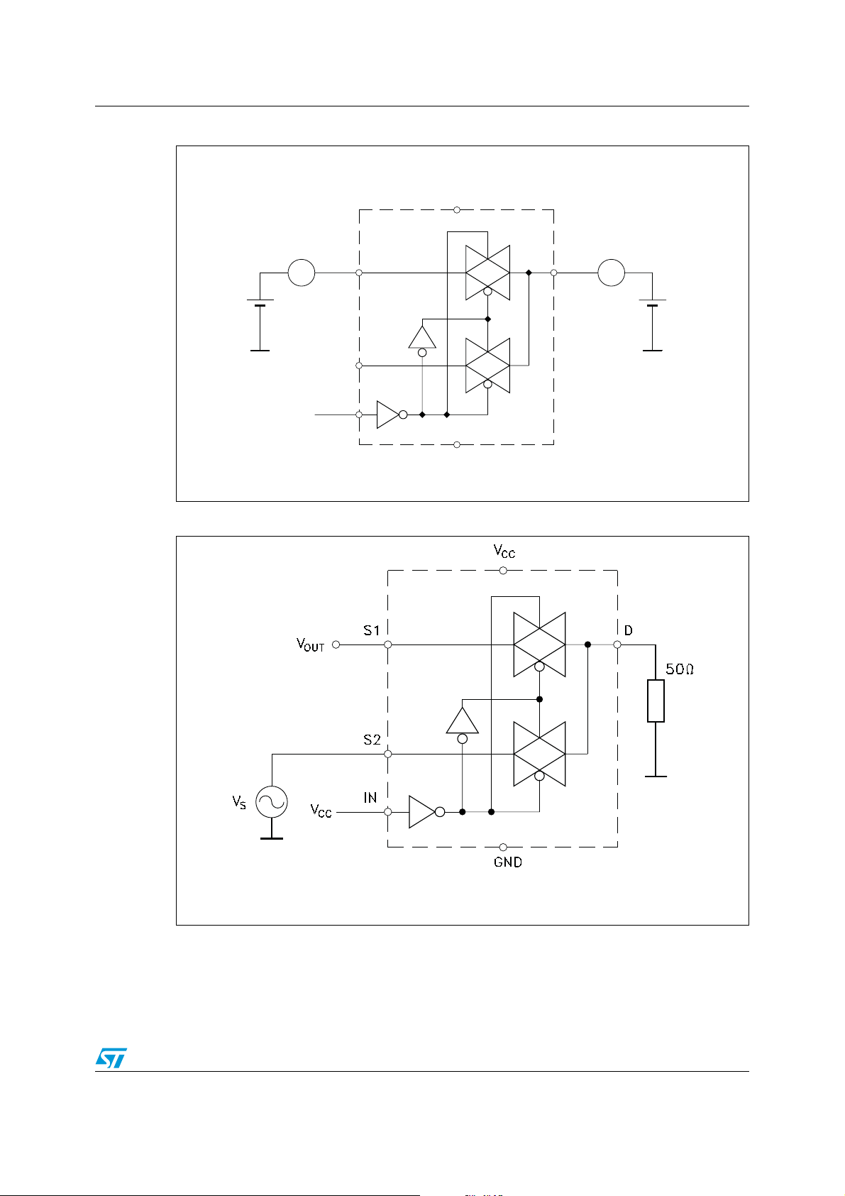
Figure 6. OFF leakage
V
CC
I
S(OFF)
A
V
SS
S2
V
CC
Figure 7. Channel-to-channel crosstalk
IN
GND
I
D(OFF)
D
A
V
D
CS14081
CS14091
11/19
Page 12
Test circuits STG4160
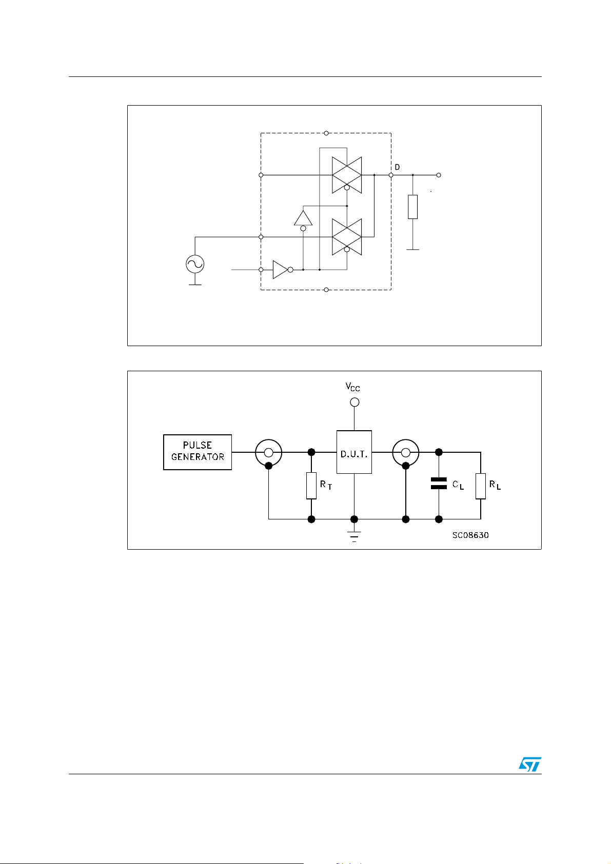
Figure 8. OFF isolation
V
CC
GND
V
S
Figure 9. Test circuit
S1
S2
IN
GND
50 Ω
V
OUT
CS00381
1. CL = 5/35 pF or equivalent: (includes jig capacitance)
= 50 Ω or equivalent
2. R
L
= Z
3. R
T
of pulse generator (typically 50 Ω )
OUT
12/19
Page 13
STG4160 Test circuits
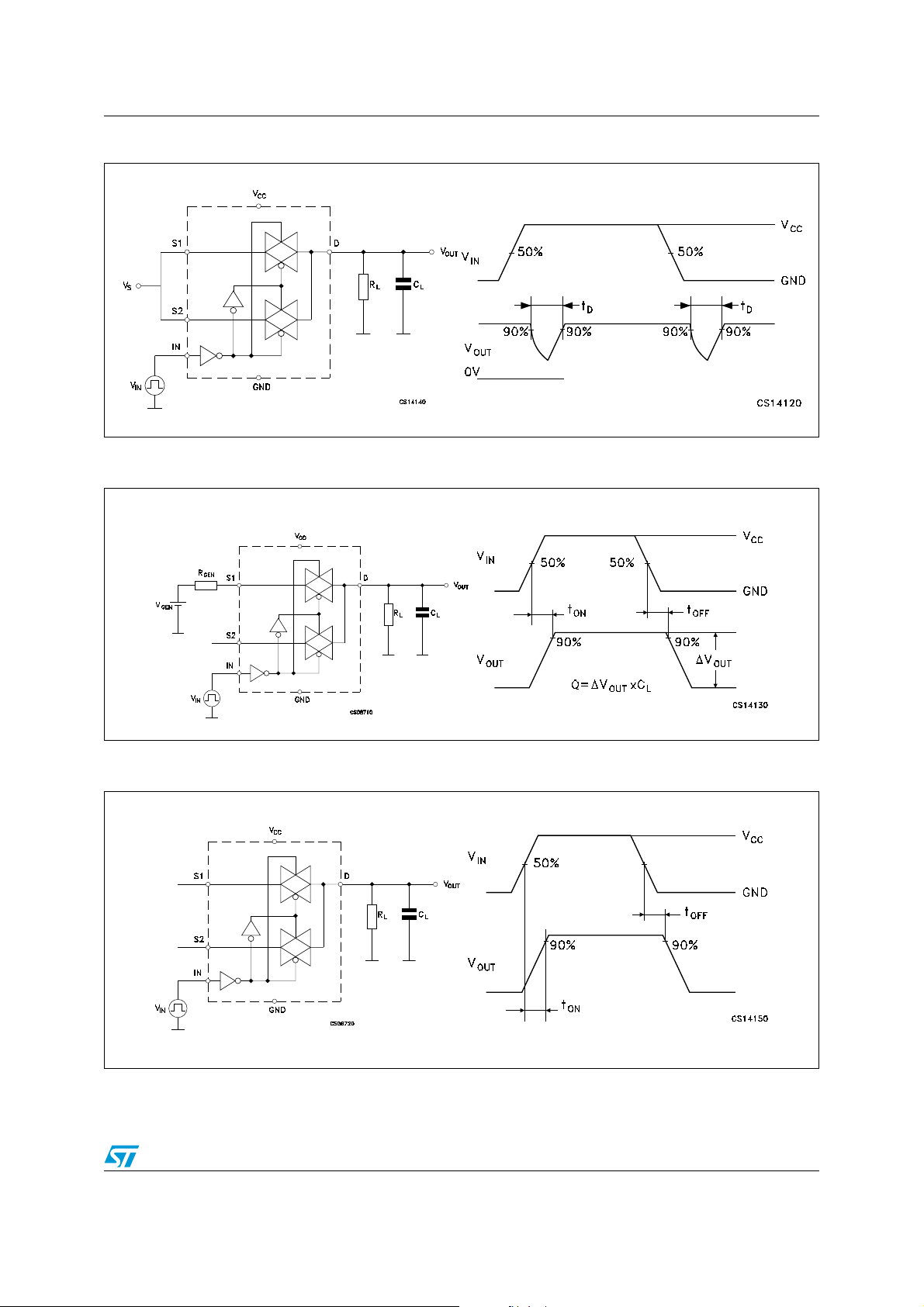
Figure 10. Break-before-make time delay
Figure 11. Switching time and charge injection
(V
GEN
=0V, R
=0Ω, RL=1MΩ, CL= 100 pF)
GEN
Figure 12. Turn ON, turn OFF delay time
13/19
Page 14
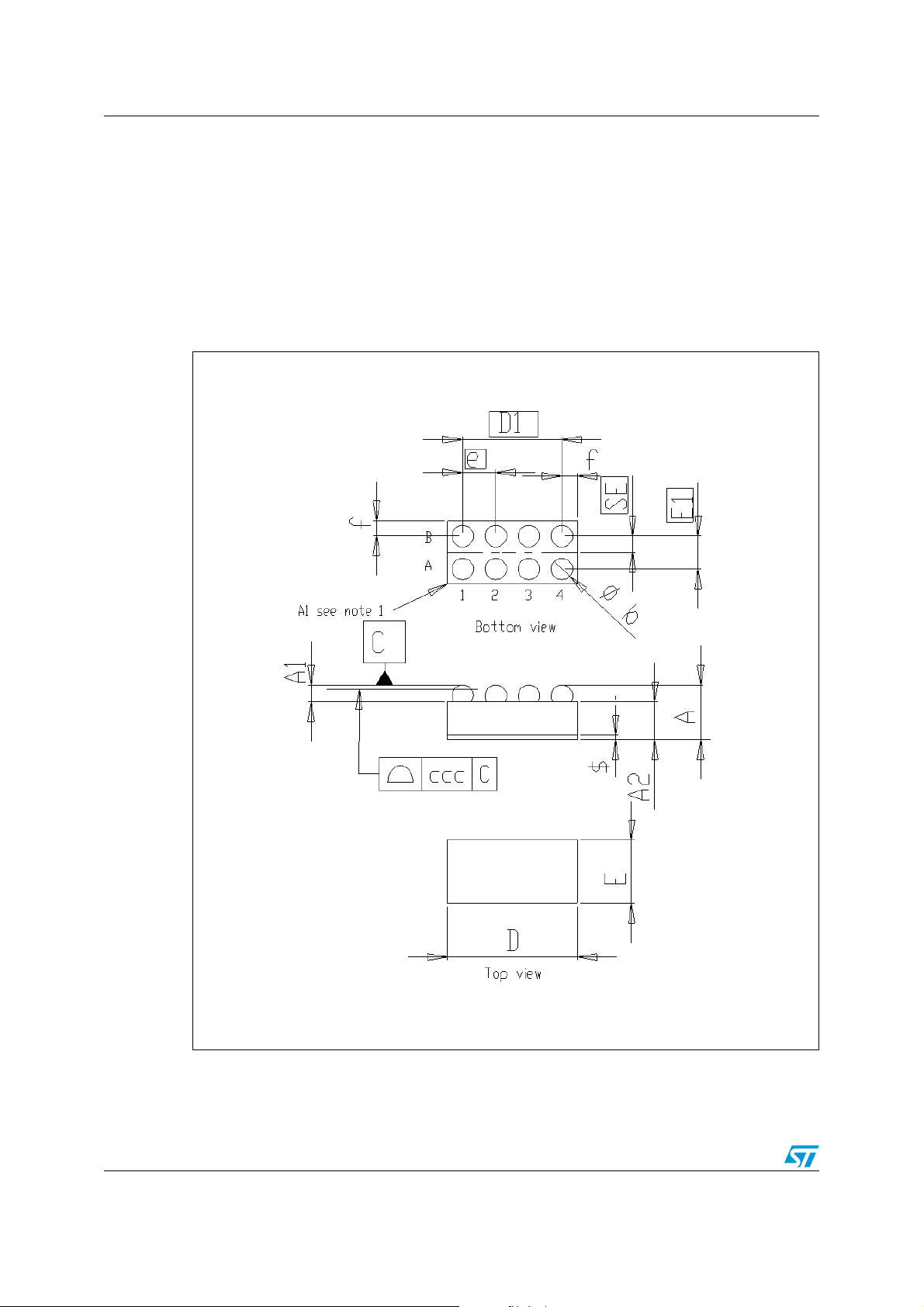
Package mechanical data STG4160
6 Package mechanical data
In order to meet environmental requirements, ST offers these devices in ECOPACK®
packages. These packages have a Lead-free second level interconnect. The category of
second Level Interconnect is marked on the package and on the inner box label, in
compliance with JEDEC Standard JESD97. The maximum ratings related to soldering
conditions are also marked on the inner box label. ECOPACK is an ST trademark.
ECOPACK specifications are available at: www.st.com.
Figure 13. Flip-chip 8 package outline
1. Drawing not to scale.
14/19
Page 15
STG4160 Package mechanical data
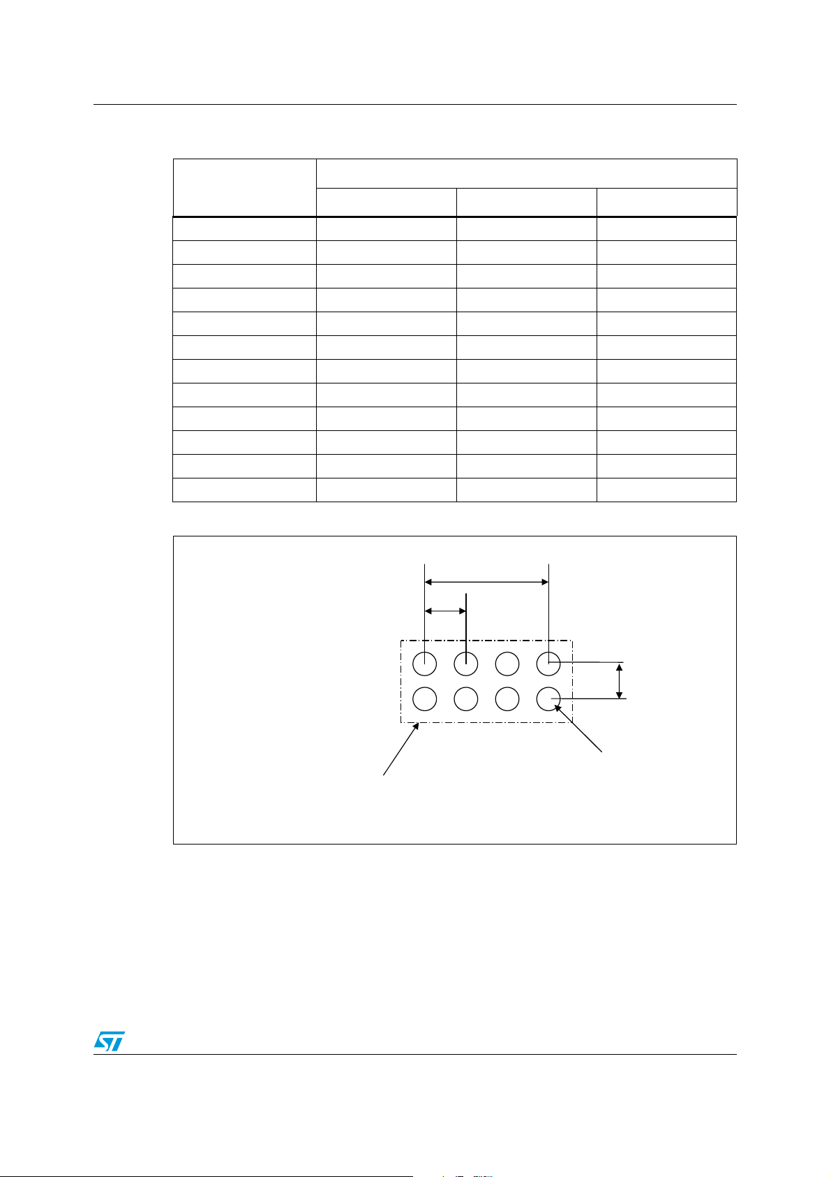
Table 9. Flip-chip 8 mechanical data
Millimeters
Symbol
Min Typ Max
A 0.535 0.58 0.625
A1 0.18 0.205 0.23
A2 0.355 0.375 0.395
b 0.215 0.255 0.295
D 1.85 1.9 1.95
D1 1.5
e 0.45 0.5 0.55
E 0.85 0.9 0.95
E1 0.45 0.5 0.55
SE 0.25
f 0.19 0.2 0.21
ccc 0.08
Figure 14. Flip-chip 8 footprint
GRID PLACEMENT AREA
A
B
1.5
0.5
12
3
0.5
4
0.22
15/19
Page 16
Package mechanical data STG4160
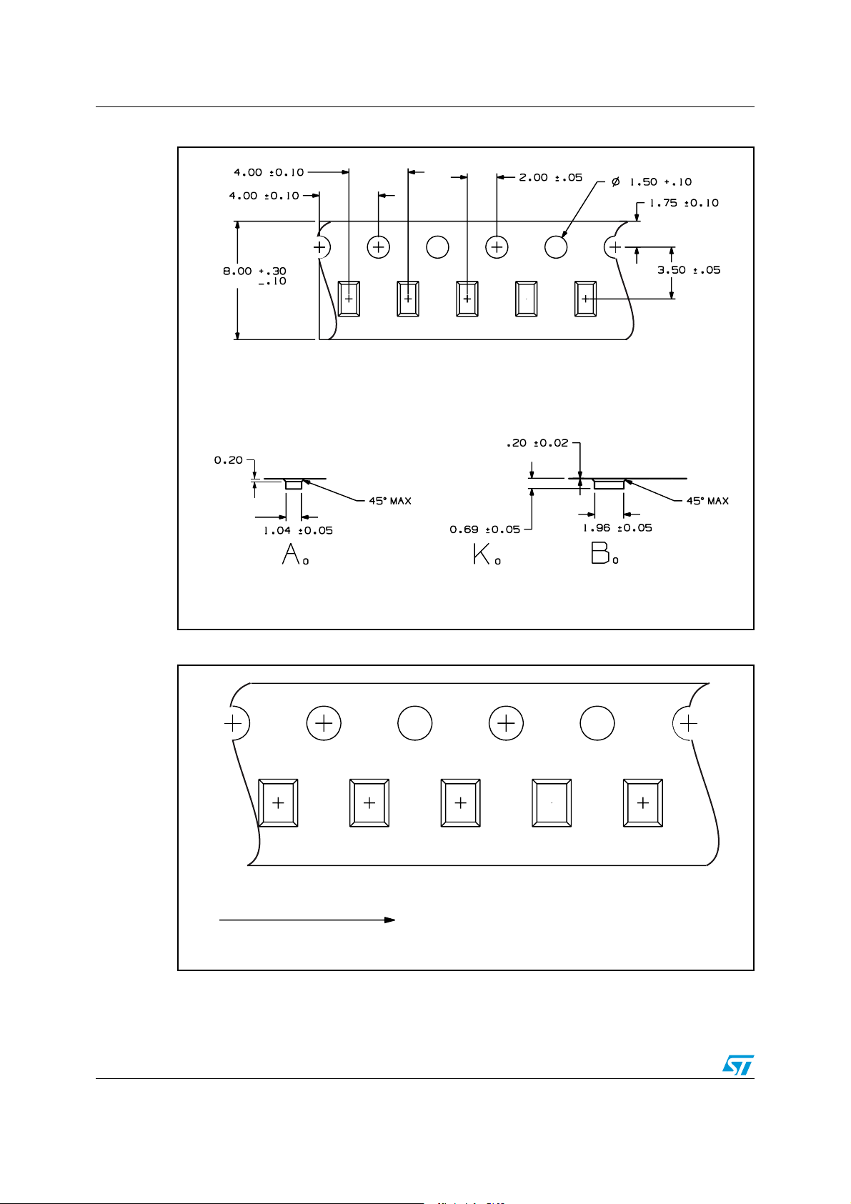
Figure 15. Flip-chip 8 tape and reel
Figure 16. Tape orientation
5SERDIRECTIONOFFEED
!-6
!-6
16/19
Page 17
STG4160 Package mechanical data
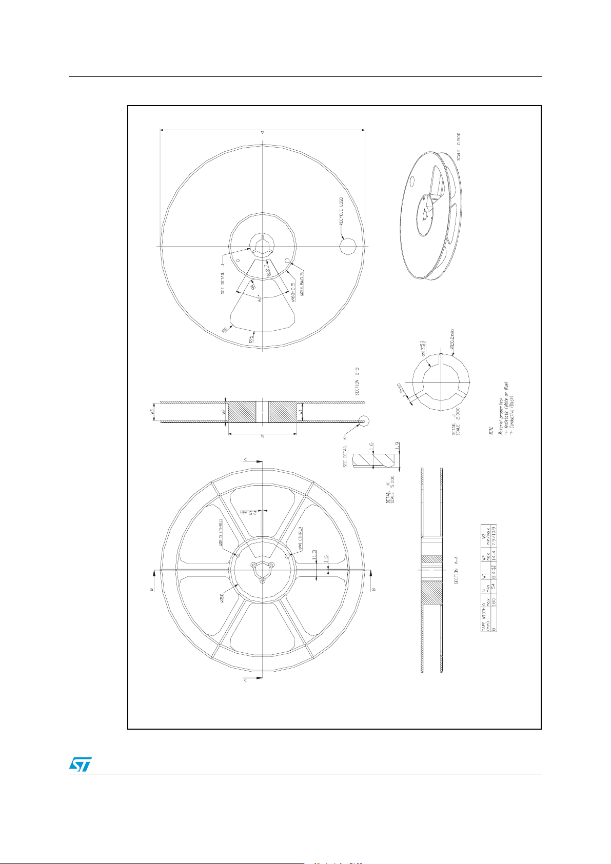
Figure 17. Reel information
17/19
Page 18
Revision history STG4160
7 Revision history
Table 10. Document revision history
Date Revision Changes
11-Sep-2008 1 Initial release.
19-Feb-2009 2 Updated: ION values in Table 6: DC specifications.
18/19
Page 19

STG4160
Please Read Carefully:
Information in this document is provided solely in connection with ST products. STMicroelectronics NV and its subsidiaries (“ST”) reserve the
right to make changes, corrections, modifications or improvements, to this document, and the products and services described herein at any
time, without notice.
All ST products are sold pursuant to ST’s terms and conditions of sale.
Purchasers are solely responsible for the choice, selection and use of the ST products and services described herein, and ST assumes no
liability whatsoever relating to the choice, selection or use of the ST products and services described herein.
No license, express or implied, by estoppel or otherwise, to any intellectual property rights is granted under this document. If any part of this
document refers to any third party products or services it shall not be deemed a license grant by ST for the use of such third party products
or services, or any intellectual property contained therein or considered as a warranty covering the use in any manner whatsoever of such
third party products or services or any intellectual property contained therein.
UNLESS OTHERWISE SET FORTH IN ST’S TERMS AND CONDITIONS OF SALE ST DISCLAIMS ANY EXPRESS OR IMPLIED
WARRANTY WITH RESPECT TO THE USE AND/OR SALE OF ST PRODUCTS INCLUDING WITHOUT LIMITATION IMPLIED
WARRANTIES OF MERCHANTABILITY, FITNESS FOR A PARTICULAR PURPOSE (AND THEIR EQUIVALENTS UNDER THE LAWS
OF ANY JURISDICTION), OR INFRINGEMENT OF ANY PATENT, COPYRIGHT OR OTHER INTELLECTUAL PROPERTY RIGHT.
UNLESS EXPRESSLY APPROVED IN WRITING BY AN AUTHORIZED ST REPRESENTATIVE, ST PRODUCTS ARE NOT
RECOMMENDED, AUTHORIZED OR WARRANTED FOR USE IN MILITARY, AIR CRAFT, SPACE, LIFE SAVING, OR LIFE SUSTAINING
APPLICATIONS, NOR IN PRODUCTS OR SYSTEMS WHERE FAILURE OR MALFUNCTION MAY RESULT IN PERSONAL INJURY,
DEATH, OR SEVERE PROPERTY OR ENVIRONMENTAL DAMAGE. ST PRODUCTS WHICH ARE NOT SPECIFIED AS "AUTOMOTIVE
GRADE" MAY ONLY BE USED IN AUTOMOTIVE APPLICATIONS AT USER’S OWN RISK.
Resale of ST products with provisions different from the statements and/or technical features set forth in this document shall immediately void
any warranty granted by ST for the ST product or service described herein and shall not create or extend in any manner whatsoever, any
liability of ST.
ST and the ST logo are trademarks or registered trademarks of ST in various countries.
Information in this document supersedes and replaces all information previously supplied.
The ST logo is a registered trademark of STMicroelectronics. All other names are the property of their respective owners.
© 2009 STMicroelectronics - All rights reserved
STMicroelectronics group of companies
Australia - Belgium - Brazil - Canada - China - Czech Republic - Finland - France - Germany - Hong Kong - India - Israel - Italy - Japan -
Malaysia - Malta - Morocco - Singapore - Spain - Sweden - Switzerland - United Kingdom - United States of America
www.st.com
19/19
 Loading...