

查询STGB3NB60SD供应商
STGB3NB60SD
N-CHANNEL 3A - 600V D2PAK
Power MESH™ IGBT
TYPE
V
CES
V
CE(sat)
I
c
STGB3NB60SD 600 V <1.5 V 3 A
■ HIGH INPUT IMPEDANCE
(VOLTAGE DRIVEN)
■ VERY LOW ON-VOLTAGE DROP (V
■ HIGH CURRENT CAPABILITY
■ OFF LOSSES INCLUDE TAIL CURRENT
■ INTEGRATED FREEWHEELING DIODE
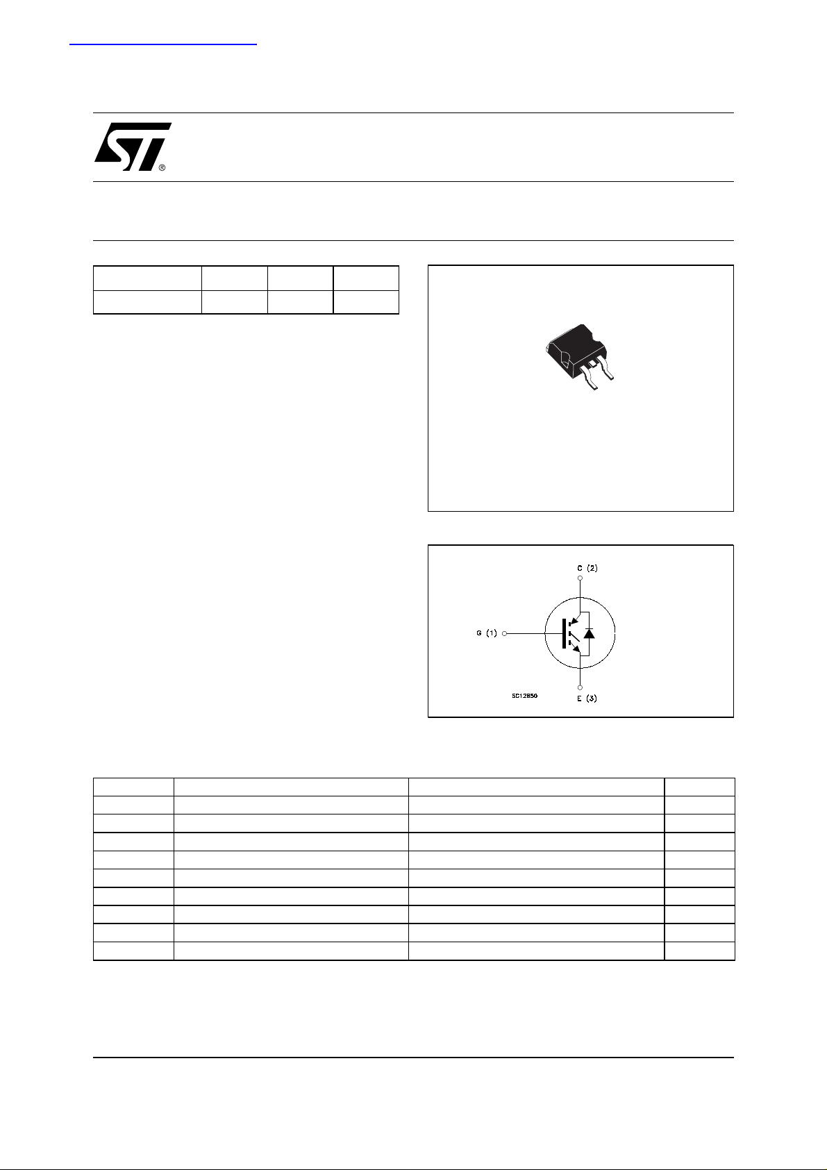
■ SURFACE-MOUNTING D
2
PAK (TO-263)
cesat
)
POWER PACKAGE IN TAPE & REEL
(SUFFIX “T4”)
DESCRIPTION
Using the latest high voltage technology based on a
patented strip layout, STMicroelectronics has designed
an advanced fa mily o f IGB Ts, the PowerMESH™ IGB Ts,
with outstanding pe rfomances . The suffix “S” identifi es a
family optimized to a chiev e minim um on -volta ge drop for
low frequency applications (<1kHz).
APPLICATIONS
■ GAS DISCHARGE LAMP
■ STATIC RELAYS
■ MOTOR CONTROL
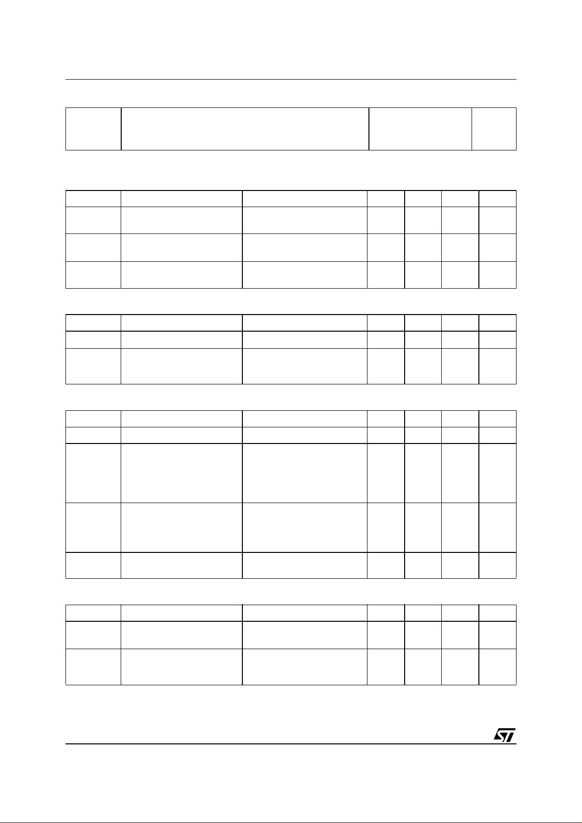
3
1
D2PAK
TO-263
(suffix“T4”)
INTERNAL SCHEMATIC DIAGRAM
ABSOLUTE MAXIMUM RATINGS
Symbol Parameter Value Unit
V
CES
V
GE
I
C
I
C
(•) Collector Current (pulsed) 25 A
I
CM
P
tot
T
stg
T
j
(•)Pulse w id th limited by s afe operating area.
Collector-Emitter Voltage (VGS = 0) 600 V
Gate-Emitter Voltag e ± 20 V
Collector Current (continuos) at Tc=25°C 6 A
Collector Current (continuos)at Tc=100°C 3 A
Total Dissipation at Tc = 25°C 70 W
Derating Factor 0.46 W/°C
Storage Temperature –60 to 175 °C
Max. Operating Junction Temperature 175 °C
1/8November 2000
STGB3NB60SD
THERMA L D ATA
R
thj-case
R
thj-amb
R
thc-sink
Thermal Resistance Junction-case Max 2.14 °C/W
Thermal Resistance Junction-ambient Max 62.5 °C/W
Thermal Resistance Case-sink Typ 0.5 °C/W
ELECTRICAL CHARACTERISTICS (T
= 25 °C unless otherwise specified)
case
OFF
Symbol Parameter Test Conditions Min. Typ. Max. Unit
V
BR(CES)
Collector-Emitter
ID = 250 µA VGE = 0 600
Breakdown Voltage
Collector cut-off (VGE = 0) VCE = Max Rating Tj = 25 °C
V
= Max Rating Tj = 125 °C
CE
Gate-body Leakage
Current (V
DS
= 0)
V
= ± 20V VCE = 0
GS
10
100
±100 nA
ON
(*)
I
CES
I
GSS
Symbol Parameter Test Conditions Min. Typ. Max. Unit
V
V
GE(th)
V
CE(SAT)
Gate Threshold Voltage
Collector-Emitter Saturation
Voltage
= VGE I
CE
= 15 V IC = 1.5 A
V
GE
= 15 V IC = 3 A
V
GE
V
= 15 V ID = 3 A Tj = 125 °C
GE
= 250 µA
C
2.5 5 V
1
1.2
1.5
1.1
DYNAMIC
Symbol Parameter Test Conditions Min. Typ. Max. Unit
g
fs
C
ies
C
oes
C
res
Forward Transconductance VCE = 25 V IC = 3 A 1.7 2.5 S
Input Capacitance VCE = 25V f = 1 MHz VGE = 0 255 330 pF
Output Capacitance 30 40 pF
Reverse Transfer Capacitanc-
5.6 7 pF
es
V
µA
µA
V
V
V
Q
G
Q
GE
Q
GC
I
CL
Total Gate Charge VCE=480V IC=3 A VGE=15 V 18 nC
Gate-Emitter Charge 5.4 nC
Gate-Collector Charge 5.5 nC
Latching Current V
= 480 V RG = 1 K
clamp
T
=150 °C
j
12 A
Ω
SWITCHING ON
Symbol Parameter Test Conditions Min. Typ. Max. Unit
125
150
50
1100
2/8
t
d(on)
t
(di/dt)
E
on
DelayTime
r
Rise Time
Turn-on Current Slope
on
Turn-on Switching Losses
VCC = 480 V IC = 3 A
= 15 V RG = 1 k
V
GE
VCC = 480 V IC = 3 A
= 15 V RG = 1 k
V
GE
T
=125 °C
j
Ω
Ω
ns
ns
A/µs
J
µ
STGB3NB60SD
ELECTRICAL CHARACTERISTICS (continued)
SWITCHING OFF
Symbol Parameter Test Conditions Min. Typ. Max. Unit
= 480 V IC = 3 A
V
CC
= 1 k
R
GE
V
CC
R
GE
T
j
Ω
= 480 V IC = 3 A
= 1 k
Ω
= 125 °C
VGE = 15 V
VGE = 15 V
tr(
t
d(Voff
E
off(**
tr(
t
d(Voff
E
off(**
t
c
Voff
t
f
t
c
Voff
t
f
Cross-Over Time
)
Off Voltage Rise Time
)
Delay Time
Fall Time
)
Turn-off Switching Loss
Cross-Over Time
)
Off Voltage Rise Time
)
Delay Time
Fall Time
)
Turn-off Switching Loss
COLLECTOR-EMITTER DIODE
Symbol Parameter Test Conditions Min. Typ. Max. Unit
I
f
I
fm
V
t
rr
Q
rr
I
rrm
(•)Pulse width li m i ted by max. junction temperature
(*)Pulsed: Pulse dur ation = 300 µs, duty cycle 1. 5 %.
(∗∗)Losses I nclude Also T he Tail (Jedec St andardization)
Forward Current
Forward Current pulsed
Forward On-Voltage
f
Reverse Recovery Time
Reverse Recovery Charge
Reverse Recovery Current
= 3 A
I
f
= 1 A
I
f
If = 3 A VR = 200 V
di/dt = 100 A/µs T
= 125 °C
j
1.8
1.0
3.4
0.72
1.15
2.8
1.45
3.6
1.2
1.8
1.55
1.15
1700
4500
9.5
3
25
1.9 V
µ
µ
µ
µ
mJ
µ
µ
µ
µ
mJ
A
A
V
ns
nC
A
s
s
s
s
s
s
s
s
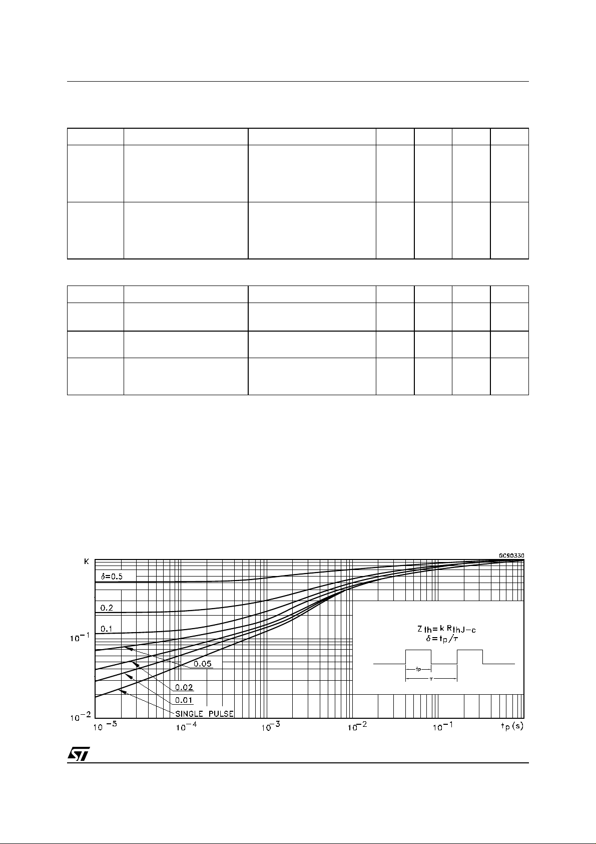
Thermal Impedance
3/8

STGB3NB60SD
Output Characteristic s Transfer Characteristics
Transconductance Collector-Emitter on Voltage vs Temperature
Collector-Emiter on Voltage vs Collector Current Gate Threshold vs Temperature
4/8

Normalized Breakdown Voltage vs Temperature Capacitance Variations
Gate charge Gate-Emitter Voltage Off Switching Losses vs Ic
STGB3NB60SD
Off Switching Losses vs Tj Swittching Off Safe Operating Area
5/8

STGB3NB60SD
Diode Forward vs Tj Diode Forward Voltage
Fig. 1: Gate Charge test Circuit Fig. 2 Test Circuit For Inductive Load Switching
Fig. 3: Switch ing W a ve f o rms
6/8

D2PAK MECHANICAL DATA
STGB3NB60SD
DIM.
A 4.4 4.6 0.173 0.181
A1 2.49 2.69 0.098 0.106
A2 0.03 0.23 0.001 0.009
B 0.7 0.93 0.027 0.036
B2 1.14 1.7 0.044 0.067
C 0.45 0.6 0.017 0.023
C2 1.23 1.36 0.048 0.053
D 8.95 9.35 0.352 0.368
D1 8 0.315
E 10 10.4 0.393
E1 8.5 0.334
G 4.88 5.28 0.192 0.208
L 15 15.85 0.590 0.625
L2 1.27 1.4 0.050 0.055
L3 1.4 1.75 0.055 0.068
M 2.4 3.2 0.094 0.126
R 0.4 0.015
V2 0º8º
MIN. TYP MAX. MIN. TYP. MAX.
mm. inch
7/8

STGB3NB60SD
Information furnished is believed to be accurate and reliable. However, STM ic roelectronics assumes no responsi bility for the consequ ences
of use of such information nor for any infringement of patents or other rights of third parties which may result from its use. No license is granted
by implic ation or o th erwise under any patent or patent rights of STMi croelectronics. Sp ecifications menti oned in thi s publication are subject
to change without notice. This publication supersedes and replaces all information previously supplied. STMicroelectronics products are not
authorized for use as cri tical comp onents in lif e support dev i ces or systems wi thout exp ress written approval of STMicroel ectronics.
The ST log o i s registered trademark of STMicroelectronics
© 20 00 STMicroelectronics - All Rig hts Reserved
All other names are the property of their respective ow ners.
Australi a - Brazil - Ch i na - Finland - F rance - Germ any - Hong Kong - India - Italy - Japan - Malaysia - Mal t a - Morocc o -
Singapor e - Spain - Sweden - Switz erl and - United Kingdom - U.S.A.
STMicroelect ro n ics GRO UP OF COMPANI ES
http://www.st.com
8/8
 Loading...