

Sony STRDG-820 Service manual
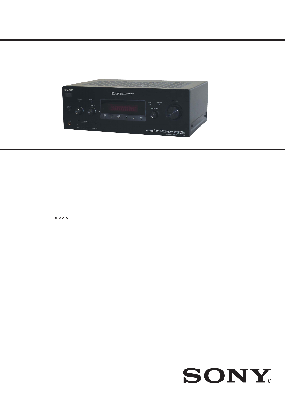
STR-DG820
SERVICE MANUAL
Ver. 1.1 2008.08
This receiver incorporates Dolby* Digital and Pro Logic Surround and the DTS** Digital Surround System.
* Manufactured under license from Dolby Laboratories. Dolby, Pro Logic, Surround Ex, and the double-D
symbol are trademarks of Dolby Laboratories.
** Manufactured under license under U.S. Patent #’s: 5,451,942; 5,956,674; 5,974,380; 5,978,762; 6,226,616;
6,487,535 & other U.S. and worldwide patents issued & pending. DTS is a registered trademark and the
DTS logos, Symbol, DTS-HD and DTS-HD Master Audio are trademarks of DTS, Inc. © 1996-2007 DTS,
Inc. All Rights Reserved.
This receiver incorporates High-Definition Multimedia Interface (HDMITM) technology.HDMI, the HDMI
logo and High-Definition Multimedia Interface are trademarks or registered trademarks of HDMI Licensing LLC.
XM Ready® is a registered trademark of XM Satellite Radio Inc. All rights reserved.
This product is manufactured under license from Neural Audio Corporation and THX Ltd. Sony Corporation
hereby grants the user a non-exclusive, non-transferable, limited right of use to this product under USA and
foreign patent, patent pending and other technology or trademarks owned by Neural Audio Corporation and THX
Ltd. “Neural Surround”, “Neural Audio”, “Neural” and “NRL” are trademarks and logos owned by Neural Audio
Corporation, THX is a trademark of THX Ltd., which may be registered in some jurisdictions. All rights reserved.
“x.v.Color” and “x.v.Color” logo are trademarks of Sony Corporation.
“BRAVIA” and are trademarks of Sony Corporation.
US Model
Canadian Model
AEP Model
UK Model
E Model
Australian Model
AUDIO POWER
SPECIFICATIONS (US model)
POWER OUTPUT AND TOTAL
HARMONIC DISTORTION:
With 8 ohm loads, both channels driven, from
20Hz–20,000Hz;rated100wattsper
channel minimum RMS power, with no more
than 0.09% total harmonic distortion from 250
milliwatts to rated output.
Amplifier section
Models of area code U, CA
Power Output
Minimum RMS Output Power
(8 ohms, 20 Hz – 20 kHz , THD 0.09%)
Stereo Mode Output Pow er
(8 ohms, 1 kHz, THD 0.7%)
Surround Mode Output Power
(8 ohms, 1 kHz, THD 10% )
1)
100 W + 100 W
110 W + 110 W
2)
150 W per channel
SPECIFICATIONS
Models of area code CEL, CEK, ECE, AU,
1)
TW, E51
Minimum RMS Output Power
(8 ohms, 20 Hz – 20 kHz, THD 0.09%)
Stereo Mode Output Power
(8 ohms, 1 kHz, THD 0.7%)
Surround Mode Output Powe r
(8 ohms, 1 kHz, THD 10%)
Models of area code KR
Minimum RMS Output Power
(8 ohms, 20 Hz – 20 kHz, THD 0.09%)
Stereo Mode Output Power
(8 ohms, 1 kHz, THD 0.7%)
Surround Mode Output Powe r
(8 ohms, 1 kHz, THD 10%)
85 W + 85 W
100 W + 100 W
2)
140 W per channel
1)
75 W + 75 W
90 W + 90 W
2)
130 W per channel
1)
Measured under the following co nditions:
Area code Power requirements
U, CA 120 V AC, 60 Hz
CEL, CEK, ECE 230 V AC, 50 Hz
AU, E51 240 V AC, 50 Hz
TW 110 V AC, 60 Hz
KR 220 V AC, 60 Hz
2)
Reference power output forfront, center, surround
and surround back speakers. Depend ing on the
sound field settings and the source , there may be
no sound output.
Frequency response
Analog 10 Hz – 70 kHz,
Input
Analog Sensitivity: 500 mV/
+0.5/–2 dB (with sound
field and equalizer
bypassed)
50 kohms
3)
S/N
:96dB
4)
(A, 500 mV
)
MULTI CHANNEL AV RECEIVER
Digital (Coaxial) Impedance: 75 ohms
Digital (Optical) S/N: 100 dB
Output (analog)
AUD IO O UT Volta ge: 50 0 mV/
SUBWOOFER Voltage: 2 V/1 kohm
Equalizer
Gain levels ±10 dB, 1 dB step
3)
INPUT SHORT (with sound field and equalizer
bypassed).
4)
Weighted network, input level.
FM tuner section
Tuning range 87.5 MHz – 108.0 MHz
Antenna (aerial) FM wire antenna (aerial)
Antenna (aerial) terminals
Intermediate frequency
S/N: 100 dB
(A, 20 kHz LPF)
(A, 20 kHz LPF)
10 kohms
75 ohms, unbalanced
10.7 MHz
– Continued on next page –
9-889-096-02
2008H05-1
2008.08
©
Sony Corporation
Audio&Video Business Group
Published by Sony Techno Create Corporation
STR-DG820
Ver. 1.1
AM tuner section
Tuning range
Area code Tuning scale
U, CA 530 kHz –
CEL, CEK, ECE – 531 kHz –
AU, E51 530 kHz –
KR, TW 530 kHz –
Antenna (aerial) Loop antenna
Intermediate frequency
5)
You can change the AM tuning scale to 9 kHz or
10 kHz. After tuning in any AM station, turn off
the receiver. While holding down TUNING
MODE, press POWER on the receiver. All preset
stations will beerase dwhen you change the tuning
scale. To reset the scale to 10 kHz (or 9 kHz),
repeat the procedure.
Video section
Inputs/Outputs
Video: 1 Vp-p, 75 ohms
COMPONENT VIDEO:
General
Power requirements
Area code Power requirements
U, CA 120 V AC, 60 Hz
CEL, CEK, ECE 230 V AC, 50/6 0 Hz
AU 240 V AC, 50 Hz
TW 110 V AC, 60 Hz
KR 220 - 230 V AC, 50/60 Hz
E51 120/220/240 V AC, 50/60 Hz
Power output (DIGITAL MEDIA PORT)
DC OUT: 5V , 0.7 A MAX
Power consumption
Area code Power consumption
U 250 W
CA 320 VA
CEL, CEK, ECE,
AU, KR, E51
TW 220 W
Power consumption (during standby mode)
Dimensions (width/heigh t/depth) (Approx.)
Mass (Approx.) 18 lb 12 oz (8.5 kg) (U, CA)
Supplied accessories
Operating instructions
Quick Setup Guide (1)
FM wire antenna (aerial) (1)
AM loop antenna (aeri al) (1)
Remote commander (R M-AAP021) (1)
R6 (size-AA) batteries (2)
Optimizer microphone (ECM-AC2) (1)
Design and specifications are subject to
change without notice.
About area codes
The area code of the receiver you purchased is
shown on the lower right po rtion of the rear panel
(see the illustration below).
SURROUND BACK
L
CENTER
R
SPEAKERS
R
SPEAKERS
Any differences in operation, according to the area
code, are clearly indicat ed in the text, for example,
“Models of area co de AA only”.
SURROUND
L
R
FRONT AFRONT B
L
L
R
10 kHz step 9 kHz step
1,710 kHz
1,710 kHz
1,610 kHz
450 kHz
Y: 1 Vp-p, 75 ohms
P
P
80 MHz HD Pass Throu gh
230 W
0.7 W
(When “CTRL:H DMI” in
HDMI menu is set to
“CTRL OFF”)
17 × 6 1/4 × 12 5/8 inches
(430 × 157.5 × 318 mm)
including proje cting parts
and controls
531 kHz –
5)
1,710 kHz
1,602 kHz
531 kHz –
5)
1,710 kHz
531 kHz –
5)
1,602 kHz
B/CB:0.7Vp-p,75ohms
R/CR:0.7Vp-p,75ohms
8.4 kg (CEL, CEK,
ECE, AU, TW, KR, E51)
Area code
5)
5)
5)
Notes on chip component replacement
• Never reuse a disconnected chip component.
• Notice that the minus side of a tantalum capacitor may be damaged by heat.
SAFETY CHECK-OUT
After correcting the original service problem, perform the following safety check before releasing the set to the customer:
Check the antenna terminals, metal trim, “metallized” knobs,
screws, and all other exposed metal parts for AC leakage.
Check leakage as described below.
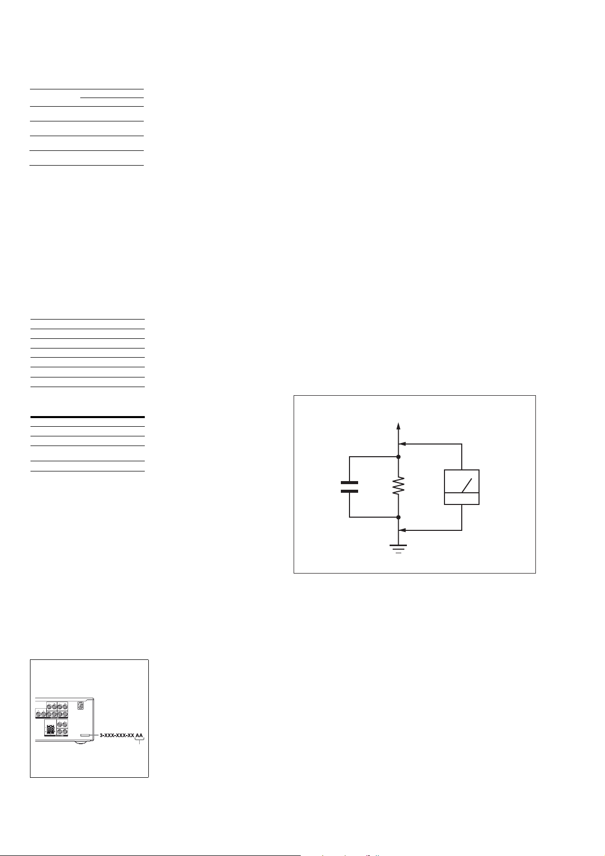
LEAKAGE TEST
The AC leakage from any exposed metal part to earth ground and
from all exposed metal parts to any exposed metal part having a
return to chassis, must not exceed 0.5 mA (500 microamperes.).
Leakage current can be measured by any one of three methods.
1. A commercial leakage tester, such as the Simpson 229 or RCA
WT-540A. Follow the manufacturers’ instructions to use these
instruments.
2. A battery-operated AC milliammeter. The Data Precision 245
digital multimeter is suitable for this job.
3. Measuring the voltage drop across a resistor by means of a
VOM or battery-operated AC voltmeter. The “limit” indication
is 0.75 V, so analog meters must have an accurate low-voltage
scale. The Simpson 250 and Sanwa SH-63Trd are examples
of a passive VOM that is suitable. Nearly all battery operated
digital multimeters that have a 2 V AC range are suitable. (See
Fig. A)
To Exposed Metal
Parts on Set
AC
1.5 kΩ0.15 μF
voltmeter
(0.75 V)
Earth Ground
Fig. A. Using an AC voltmeter to check AC leakage.
SAFETY-RELATED COMPONET WARNING!
COMPONENTS IDENTIFIED BY MARK 0 OR DOTTED LINE
WITH MARK 0 ON THE SCHEMATIC DIAGRAMS AND IN
THE PARTS LIST ARE CRITICAL TO SAFE OPERATION.
REPLACE THESE COMPONENTS WITH SONY PARTS
WHOSE PART NUMBERS APPEAR AS SHOWN IN THIS
MANUAL OR IN SUPPLEMENTS PUBLISHED BY SONY.
ATTENTION AU COMPOSANT AYANT RAPPORT
LES COMPOSANTS IDENTIFIÉS PAR UNE MARQUE 0 SUR
LES DIAGRAMMES SCHÉMATIQUES ET LA LISTE DES
PIÈCES SONT CRITIQUES POUR LA SÉCURITÉ DE FONCTIONNEMENT. NE REMPLACER CES COM- POSANTS QUE
PAR DES PIÈCES SONY DONT LES NUMÉROS SONT DONNÉS DANS CE MANUEL OU DANS LES SUPPLÉMENTS
PUBLIÉS PAR SONY.
À LA SÉCURITÉ!
2

STR-DG820
SECTION 1
SERVICING NOTES
Ver. 1.1
TABLE OF CONTENTS
1. SERVICING NOTES ............................................. 3
2. GENERAL .................................................................. 4
3. DISASSEMBLY
3-1. Disassembly Flow .......................................................... 9
3-2. Case ................................................................................. 9
3-3. Front Panel Block ........................................................... 10
3-4. Back Panel Block ........................................................... 10
3-5. Main Block ..................................................................... 11
3-6. MAIN Board ................................................................... 11
4. TEST MODE ............................................................ 12
5. ELECTRICAL CHECK ......................................... 13
6. DIAGRAMS
6-1. Block Diagram - MAIN Section - ................................... 14
6-2. Block Diagram - HDMI Section - ................................... 15
6-3. Block Diagram - DSP/XM Section - .............................. 16
6-4. Block Diagram - AUDIO Section - ................................. 17
6-5. Block Diagram - POWER SUPPLY Section - ................ 18
6-6. Printed Wiring Board - MAIN Board - ........................... 20
6-7. Schematic Diagram - MAIN Board (1/3) - ..................... 21
6-8. Schematic Diagram - MAIN Board (2/3) - ..................... 22
6-9. Schematic Diagram - MAIN Board (3/3) - ..................... 23
6-10. Printed Wiring Board
- HDMI Board (Component Side) - ................................ 24
6-11. Printed Wiring Board
- HDMI Board (Conductor Side) - .................................. 25
6-12. Schematic Diagram - HDMI Board (1/2) - ..................... 26
6-13. Schematic Diagram - HDMI Board (2/2) - ..................... 27
6-14. Printed Wiring Board
- XM Board (US, Canadian models) - ............................ 28
6-15. Schematic Diagram
- XM Board (US, Canadian models) - ............................ 29
6-16. Printed Wiring Board - DSP Board - .............................. 30
6-17. Schematic Diagram - DSP Board - ................................. 31
6-18. Printed Wiring Boards
- DIGITAL AUDIO Section (1/2) - ................................. 32
6-19. Printed Wiring Board
- DIGITAL AUDIO Section (2/2) - ................................. 33
6-20. Schematic Diagram
- DIGITAL AUDIO Section (1/2) - ................................. 34
6-21. Schematic Diagram
- DIGITAL AUDIO Section (2/2) - ................................. 35
6-22. Printed Wiring Board - MICOM Board - ........................ 36
6-23. Schematic Diagram - MICOM Board - .......................... 37
6-24. Printed Wiring Board - DISPLAY Board - ..................... 38
6-25. Schematic Diagram - DISPLAY Board - ........................ 39
6-26. Printed Wiring Board - VIDEO Board - ......................... 40
6-27. Schematic Diagram - VIDEO Board - ............................ 41
6-28. Printed Wiring Boards - PANEL Section - ..................... 42
6-29. Schematic Diagram - PANEL Section - .......................... 43
6-30. Printed Wiring Board - SPEAKER Board - .................... 44
6-31. Schematic Diagram - SPEAKER Board - ....................... 44
6-32. Printed Wiring Board - DCDC Board - .......................... 45
6-33. Schematic Diagram - DCDC Board - ............................. 45
6-34. Printed Wiring Boards - POWER Section - .................... 46
6-35. Schematic Diagram - POWER Section - ........................ 47
UNLEADED SOLDER
Boards requiring use of unleaded solder are printed with the leadfree mark (LF) indicating the solder contains no lead.
(Caution: Some printed circuit boards may not come printed with
the lead free mark due to their particular size)
: LEAD FREE MARK
Unleaded solder has the following characteristics.
• Unleaded solder melts at a temperature about 40 °C higher
than ordinary solder.
Ordinary soldering irons can be used but the iron tip has to be
applied to the solder joint for a slightly longer time.
Soldering irons using a temperature regulator should be set to
about 350 °C.
Caution: The printed pattern (copper foil) may peel away if the
heated tip is applied for too long, so be careful!
• Strong viscosity
Unleaded solder is more viscou-s (sticky, less prone to fl ow)
than ordinary solder so use caution not to let solder bridges
occur such as on IC pins, etc.
• Usable with ordinary solder
It is best to use only unleaded solder but unleaded solder may
also be added to ordinary solder.
NOTE OF REPLACING THE IC3506 AND IC3508 ON
THE HDMI BOARD
IC3506 and IC3508 on the HDMI board cannot exchange with single. When IC3506 and IC3508 on the HDMI board are damaged,
exchange the entire mounted board.
NOTE OF REPLACING THE IC5021 ON THE DSP
BOARD
IC5021 on the DSP board cannot exchange with single. When
IC5021 on the DSP board is damaged, exchange the entire mounted board.
NOTE OF REPLACING THE IC7005 ON THE MICOM
BOARD
IC7005 on the MICOM board cannot exchange with single. When
IC7005 on the MICOM board is damaged, exchange the entire
mounted board.
7. EXPLODED VIEWS
7-1. Case Section .................................................................... 70
7-2. Front Panel Section ......................................................... 71
7-3. Back Panel Section ......................................................... 72
7-4. Chassis Section ............................................................... 73
8. ELECTRICAL PARTS LIST .............................. 74
Note: Refer to supplement-1 for the HDMI and DSP boards of print-
ed wiring boards, schematic diagram and electrical parts list
of Chilean, Peruvian, Korean, Taiwan and Australian models.
3
STR-DG820
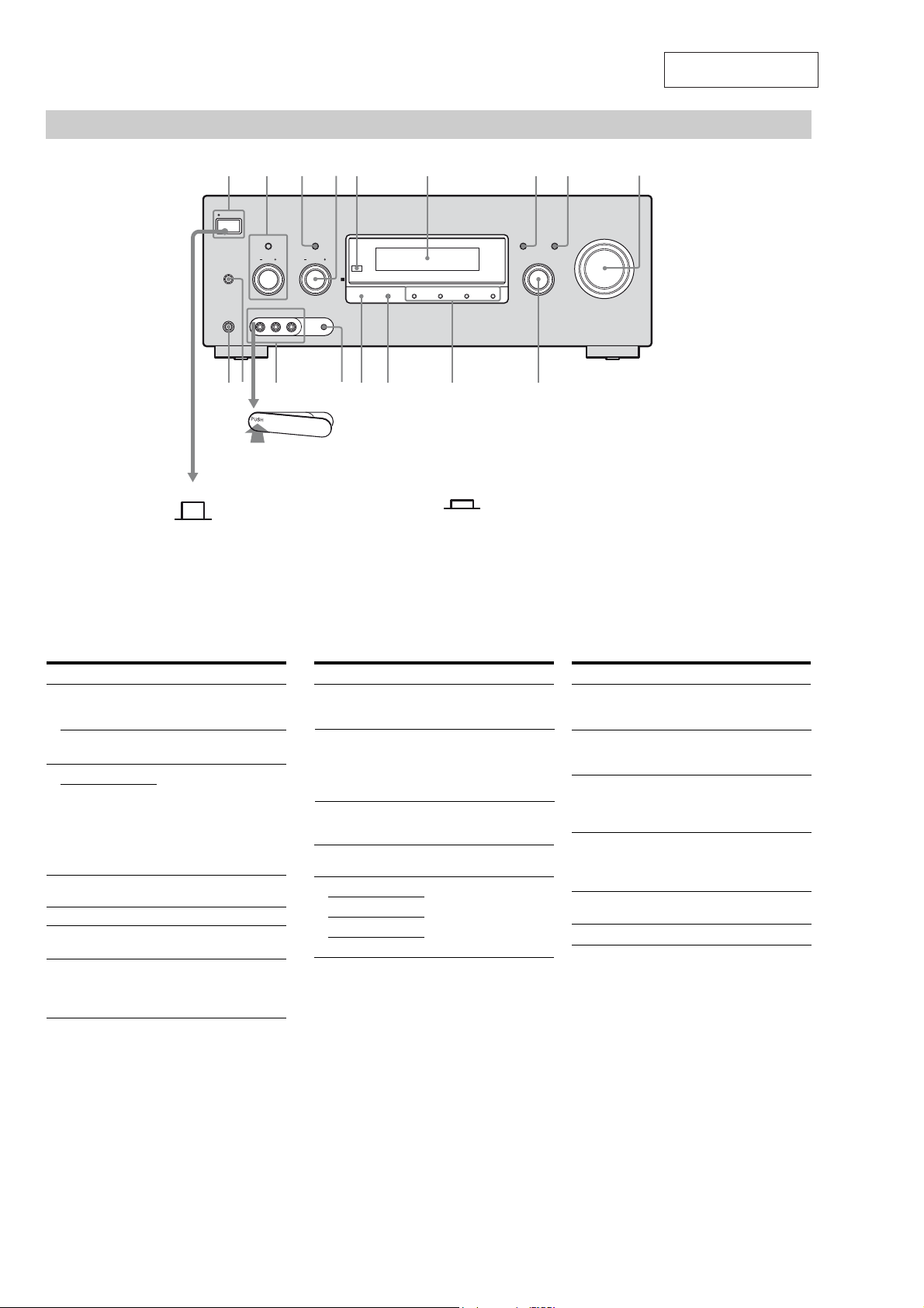
Front panel
ON/STANDBY
POWER
TONE MODE
TUNING MODE
TONE
SPEAKERS
(OFF/A/B/A+B)
PHONES
VIDEO 2 IN/PORTABLEAV IN
VIDEO L AUDIO R AUTO CAL MIC
TUNING
RKRI RE RT RB RH RG
SECTION 2
GENERAL
DISPLAY INPUT MODE
INPUT SELECTOR
MEMORY/
ENTER
To remove the cover
Press PUSH.
When you remove the cover, keep it out
of reach from children.
A.DIRECT
2CH/
A.F.D. MOVIE MUSICDIMMER
This section is extracted
from instruction manual.
MASTER VOLUME
Status of the POWER button
Off
The receiver is turned off (initial
setting).
The ON/STANDBY lamp lights off.
Press POWER to turn the receiver on.
You cannot turn the receiver on using
the remote.
Name Function
" POWER Press to turn the receiver on
ON/STANDBY
lamp
# TONE MODE Adjusts the tonal quality
TONE +/–
$ TUNING MODE Press to select the tuning
% TUNING +/– Turn toscan a station.
& Remote sensor Receives signals from
' Display window The current status of the
or off.
Show the status of the
receiver.
(bass/treble level) of the
front speakers.
Press TONE MODE
repeatedly to select bass or
treble level, then turn
TONE +/– to adjust the
level.
mode.
remote commander.
selected component or alist
of selectable items appears
here.
Name Function
( DISPLAY Press repeatedly to select
) INPUT MODE Press to select the input
* MASTER
VOLUME
+ INPUT
SELECTOR
, 2CH/A.DIRECT Press to select a sound field.
A.F.D.
MOVIE
MUSIC
information displayed on
the display.
mode when the same
components are connected
to both digital and analog
jacks.
Turn to adjust the volume
level of all speakers at the
same time.
Turn to select the input
source to playback.
On/Standby
/ on the remote to turn the
Press
receiver on or set it to the standby mode.
When you press POWER on the
receiver, the receiver will be turned off.
The ON/STANDBY lamp lights up in
green when the receiver is on.
The ON/STANDBY lamp lights up in
redwhenthereceiverissettostandby
mode.
Name Function
- DIMMER Press repeatedly to adjust
. MEMORY/
ENTER
/ AUTO CAL MIC
jack
0 VIDEO 2 IN/
PORTABLE AV
IN jacks
1 SPEAKERS
(OFF/A/B/A+B)
2 PHONES jack Connects to headphones.
the brightness of the
display.
Press to store a station or
enter the selection when
selecting the settings.
Connects to the supplied
optimizer microphone for
the Digital Cinema Auto
Calibration function.
Connects to a portable
audio/video component
such as a camcorder or
video game.
Switch to OFF, A, B, A+B
of the front speakers.
4
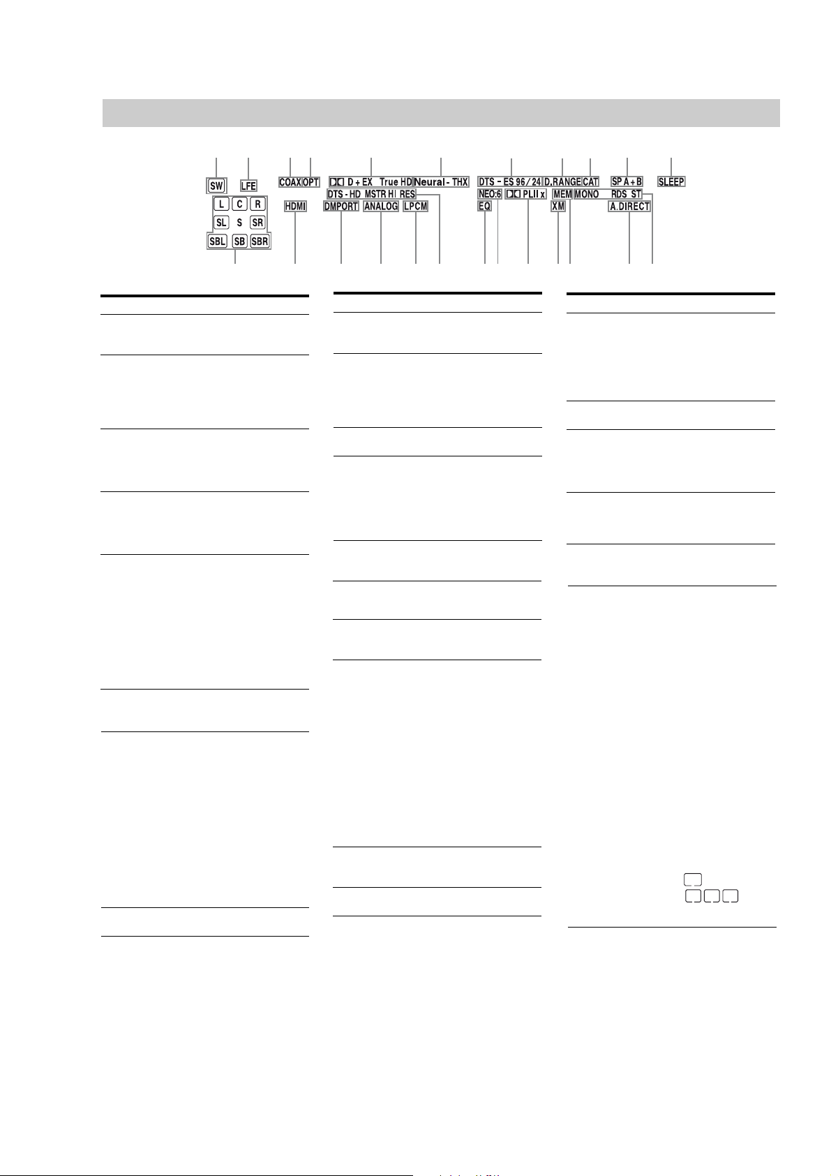
About the indicators on the display
X
R
STR-DG820
XG
Name Function
" SW Lights up when the audio signal
# LFE Lights up when the disc being
$ COAX Lights up when INPUT MODE
% OPT Lights up when INPUT MODE
&D/
D EX/
D+/
Tr ue HD
' Neural - THX Lights up when the receiver
( DTS/
DTS-ES/
DTS 96/24
) D.RANGE Lights up when dynamic range
is output from the
SUBWOOFER jacks.
played back contains an LFE
(Low Frequency Effect)
channel and the LFE channel
signal is actually being
reproduced.
is set to “AUTO” and the source
signal is a digital signal being
input through the COAXIAL
jack.
is set to “AUTO” and the source
signal is a digital signal being
input through the OPTICAL
jack.
“ D” lights up when the
receiver is decoding Dolby
Digital signals.
“D EX” lights up when the
receiver is decoding Dolby
Digital Surround EX signals.
“ D+” lights up when the
receiver is decoding Dolby
Digital Plus signals.
“ TrueHD” lights up when
the receiver is decoding Dolby
TrueHD signals.
applies Neural - THX
processing to input signals.
“DTS”lightsupwhenthe
receiver is decoding DTS
signals.
“DTS-ES” lights up when the
receiver is decoding DTS-ES
signals.
“DTS 96/24” lights up when the
receiver is decoding DTS
96 kHz/24 bit signals.
Note
When playing a DTS format
disc, besure thatyou havemade
digital connections and that
INPUT MODE is set to
“AUTO”.
compression is activated.
E
XB
XT
Name Function
* CAT Lights up when category mode
(US, Canadian
models)
+ SP A/SP B/
SP A+B
, SLEEP Lightsupwhenthesleeptimer
- Tun er
indicators
. A.DIRECT Lights up when the receiver is
/ MEM Lights up when a memory
0 XM
(US, Canadian
models)
1 PL/
PL II/
PL IIx
2 NEO:6 Lights up when DTS Neo:6
3 EQ Lights up when the equalizer is
RM
X
is set to “ONE CAT” during
XM Radio operation.
Lights up according to the
speaker system used.
However, these indicators do
not light up ifthe speaker output
is turned off or if headphones
are connected.
is activated.
Lights up when using the
receiver to tunein radio stations,
etc.
Note
“RDS” appears for models of
area code CEL, CEK, ECE
only.
processing Analog Direct
signals.
function, such as Preset
Memory etc., is activated.
Lights up when XM MiniTuner
and Home Dock are connected
and “XM RADIO” is selected.
“PL” lights up when the
receiver applies Pro Logic
processing to 2 channel signals
in order to output the center and
surround channel signals.
“PLII”lightsupwhenthe
Pro Logic II decoder is
activated.
“PL IIx” lights up when the
Pro Logic IIx decoder is
activated.
Note
Dolby Pro Logic IIx decoding
does not function for signals
with a sampling frequency of
more than 48 kHz.
Cinema/Music decoder is
activated.
activated.
RL
RK
RI
RG
H
RB
RE
RT
Name Function
4 DTS-HD
MSTR/
DTS-HD HI
RES
5 LPCM Lights up when Linear PCM
6 ANALOG Lights up when INPUT MODE
7 DMPORT Lights up when DIGITAL
8 HDMI Lights up when the receiver
9 Playback
channel
indicators
L
R
C
SL
SR
S
SB
L
SBR
SB
“DTS-HD MSTR” lights up
when the receiver is decoding
DTS-HD Master Audio signals.
“DTS-HD HI RES” lights up
when the receiver is decoding
DTS-HD High Resolution
signals.
signals are detected.
is set to “ANALOG” or no
digital signals are detected
when INPUT MODE is set to
“AUTO”.
MEDIA PORT adapter is
connected and “DMPORT” is
selected.
recognizes a component
connected via an HDMI IN jack.
The
letters(L,C,R, etc.)
indicate the channels being
played back. The boxes around
the letters vary to show how the
receiver downmixes the source
sound (based on the speaker
settings).
Front Left
Front Right
Center (monaural)
Surround Left
Surround Right
Surround (monaural or the
surround components obtained
by Pro Logic processing)
Surround Back Left
Surround Back Right
Surround Back (the surround
back components obtained by
6.1 channel decoding)
Example:
Speaker pattern: 3/0.1
Recording format: 3/2.1
Sound Field: A.F.D. AUTO
SW
LCR
SL SR
5
STR-DG820
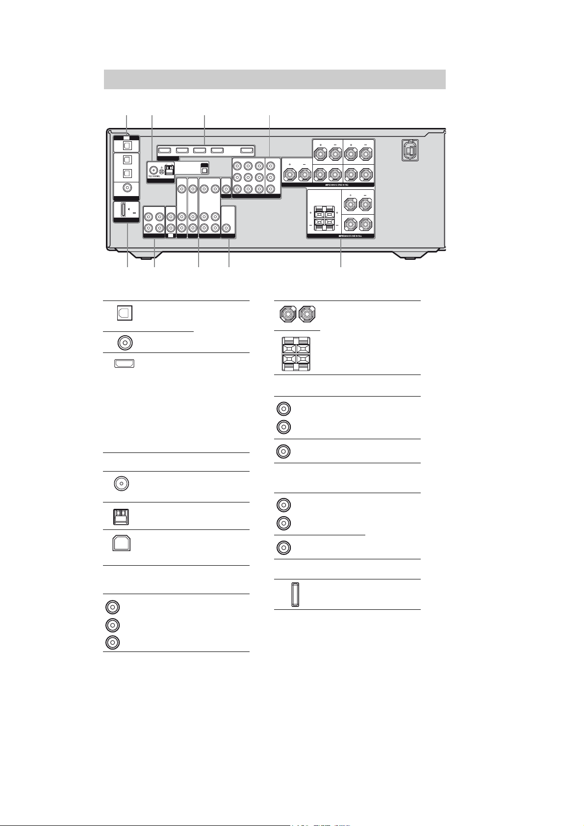
Rear panel
TV
OPTICAL
IN
VIDEO 1
IN
SAT
IN
OPTICAL
DVD
IN
COAXIAL
DIGITAL
DMPORT
(ASSIGNABLE)
DC5V
0.7A MAX
OUT IN
L
R
SA-CD/CD/CD-R
FM
ANTENNA
" DIGITAL INPUT/OUTPUT section
OPTICAL IN
jacks
COAXIAL IN
jack
HDMI IN/
OUT* jacks
# ANTENNA section
FM
ANTENNA
jack
AM
ANTENNA
terminals
XM jack Connects to the
(US, Canadian models)
$ COMPONENT VIDEO INPUT/
OUTPUT section
Y, PB/CB,PR/CR
Green
IN/OUT* jacks
(Y)
Blue
(P
B/CB)
Red
(P
)
R/CR
SAT IN DVD IN BD IN
HDMI
AM
VIDEOINVIDEO
IN
AUDIO
AUDIO
IN
IN
IN
TV
SAT
DVD
Connects toa DVD
player, etc. The
COAXIAL jack
providesabetter
sound quality.
Connects toa DVD
player, satellite
tuner, or a Blu-ray
disc player, etc.
The image is
output to a TV or a
projector while the
sound can be
output from a TV
or/and speakers
connected to this
receiver.
Connects to the
supplied FM wire
antenna.
Connects to the
supplied AM loop
antenna.
XM Mini-Tuner
and Home Dock
(not supplied).
Connects toa DVD
player, TV,
satellite tuner, etc.
XM
VIDEO
OUT
AUDIO
OUT
VIDEO 1
VIDEOINVIDEO
MONITOR
AUDIO
IN
SUBWOOFER
OUT
AUDIO
OUT
TUONI1OEDIV
SAT IN DVD IN VIDEO 1 IN MONITOR OUT
COMPONENT VIDEO
SURROUND BACK
L
CENTER
Y
B
/
P
C
B
PR/
C
R
R
SPEAKERS
R
SPEAKERS
SURROUND
L
R
FRONT AFRONT B
L
L
R
% SPEAKERS section
Connects to
speakers.
& AUDIO INPUT/OUTPUT section
AUDIO IN/
White (L)
OUT jacks
Red (R)
AUDIO OUT
Black
jack
' VIDEO/AUDIO INPUT/OUTPUT
section
AUDIO IN/
White (L)
OUT jacks
Red (R)
VIDEO IN/
Yellow
OUT* jacks
( DMPORT section
DMPORT
jack
* You can watch the selected input image when you
connect the HDMI OUT or MONITOR OUT jack
to a TV.
Connects to a
Super Audio CD
player, etc.
Connects to a
subwoofer.
Connects to a
VCR, DVD player,
etc.
Connects to a
DIGITAL MEDIA
PORT adapter.
6
STR-DG820
Ver. 1.1
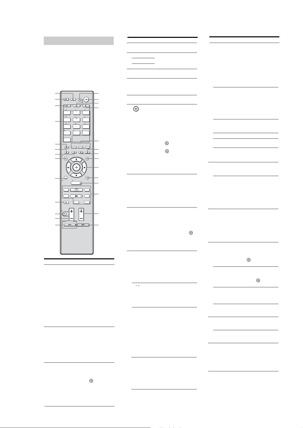
Remote commander
You can use the supplied remote to operate the
receiver and to control the Sony audio/video
components that the remote is assigned to
operate.
You can also program the remote to control
non-Sony audio/video components. Fordetails,
see “Programming the remote”.
RM-AAP021 (US, Canadian models)
RM-AAP022 (Except US, Canadian models)
XK
XI
XH
XG
XE
XT
XB
X
RM
RL
RK
RI
RH
RM SET UP
THEATER
SHIFT
VIDEO 1 VIDEO 2 BD
CLEAR
2CH/
A.DIRECT A.F.D. MOVIE MUSIC
AUTO CAL
DISPLAY
0
RETURN/
EXIT
TUNING – TUNING +
N.
DISC SKIP D.TUNING
MUTING
TOP MENU
TV INPUT
AV
SYSTEM STANDBY
TV AMP
123
456
SAT TV
DVD
789
SA-CD/
CD
ENT/MEM
0/10
-/--
/>10
XM
INPUT
SLEEP
MODE
HOME
MENU
– CATEGORY +
CATEGORY MODE
9Y
TV VOL
TV CH
MASTER VOL
PRESET
BD/DVD
F1 F2
MENU
WIDE
Name Function
" AV /
(on/standby)
# /
(on/standby)
$ TV Press to light up the button. It
Presstoturnonoroffthe
audio/video components that
the remote is programmed to
operate.
To turn the TV on or off, press
TV ($) and then press AV
/.
If you press / (#)atthe
same time, it will turn off the
receiver and other components
(SYSTEM STANDBY).
Note
The function of the AV /
switch changes automatically
each time you press the input
buttons (XG).
Press to turn the receiver on or
setittostandbymode.
To turn off all components,
press / and AV / (")at
the same time (SYSTEM
STANDBY).
To save the power in stand by
mode, set “CTRL:HDMI” to
“CTRL OFF”.
changes the remote key
function to activate the buttons
with yellow printing. It also
activate the (), 7/W/#/C
(), OPTIONSTOOLS (+),
MENU/HOME (,),
RETURN/EXIT 0 (RM), and
DISPLAY (X) buttons to
perform menu operations for
Sony TVs only.
TUNER
DMPORT
NIGHT
MODE
AMP
MENU
OPTIONS
TOOLS
RB
RT
RE
RG
Name Function
% AMP Press to light u p the button to
& A.F.D. Press to select a sound field.
MOVIE
MUSIC
' NIGHT MODE Press to activate the Night
( SLEEP Press to activate the Sleep
) AMP MENU Press to d isplay the menu to
*
,
7/W/#/C
+ OPTIONS
TOOLS
, MENU/HOME Press to display the menus of
- /
/ Press to replay the previous
N/.
a)b)
/
activate the recei ver operation.
Mode function.
Timer function and the
duration which the receiver
turns off automatically.
operate the receiver.
After pressing AMP (%),
press MENU/HOME(,)for
receiver operation, then press
7/W/# /C to select the
settings.
After pressing DVD/BD TOP
MENU (0)orDVD/BD
MENU (0), press 7/W/#/C
to select the settings, and then
press to enter the
selection.
Press alsotoenterthe
selection of the receiver,
VCR, satellite tuner, DVD
player, Blu-ray disc recor der,
PSX, DVD/VHSCOMBO, or
DVD/HDD COMBO.
Press to display and select
items from the options menus
for DVD player or Blu-ray
disc player.
To display the options of
Sony TV, press TV ($)and
then press OPTIONS
TOOLS.
the receiver, VCR, DVD
player, satellite tuner, Blu-ray
disc recorder, PSX, DVD/
VHS COMBO,or DVD/HDD
COMBO on the TV screen.
Then, use 7/W/#/C and to
perform menu operations.
To displaythe menus of Sony
TV, press TV ($)andthen
press MENU.
a)
Press to skip tracks of the
VCR, CD player, VCD
player, LD player, DVD
player, MD deck, DAT deck,
tape deck, Blu-ray disc
recorder, PSX, DVD/VHS
COMBO, or DVD/HDD
COMBO.
scene or fast forward the
current scene of the DVD
player, Blu-ray disc recor der,
DVD/VHS COMBO, or
DVD/HDD COMBO.
a)
Press to
– search tracks in the forward/
backward direction of the
CD player, VCD player,
DVD player, LD player,
MD deck, Blu-ray disc
recorder, PSX, DVD/VHS
COMBO, or DVD/HDD
COMBO.
– fast forward/rewind of the
VCR, DAT deck, or tape
deck.
Press to start playback of the
VCR, CD player, VCD
player, LD player, DVD
player, MD deck, DAT deck,
tape deck, Blu-ray disc
recorder, PSX, DVD/VHS
COMBO, or DVD/HDD
COMBO.
Name Function
a)
9
a)
Y
CATEGORY
+/–
(US, Canadian models)
TUNING +/– Press to scan a station.
D.TUNING Press to enter direct tuning
CATEGORY
MODE
(US, Canadian models)
. TV CH +
PRESET
b)
+
/–
/ F1, F2 Press F1 or F2 to select a
0 BD/DVD TOP
MENU
BD/DVD MENU Presstodisplaythemenuof
TV INPUT Press TV ($)andthen
WIDE Press TV ($)andthen
1 TV VOL +/– Press TV ($)andthen
MASTER
VOL +/–
2 MUTING Press to turn off the sound
Press to pause playback or
recording of the VCR, CD
player, VCD player, LD
player, DVD player, MD
deck, DAT deck, tape deck,
Blu-ray disc recorder, PSX,
DVD/V HS CO MBO, or
DVD/HDD COMBO. (Also
starts recordin g with
components in recor ding
standby.)
Presstostopplaybackofthe
VCR, CD player, VCD
player, LD player, DVD
player, MD deck, DAT deck,
tape deck, Blu-ray disc
recorder, PSX, DVD/VHS
COMBO, or DVD/HDD
COMBO.
Press to select a category for
XM Radio.
mode.
Press to select the category
modeforXMRadio.
b)
/– Press TV ($)andthen
press TV CH +/– to select
preset TV channels.
Press to
– select preset stations.
– select preset channels of
the VCR, satellite tuner,
Blu-ray disc recorder,
DVD player, DVD/VHS
COMBO, or DVD/HDD
COMBO.
component.
• DVD/HDD COMBO
F1: HDD mode
F2: DVD mode
• DVD/VHS COMBO
F1: DVD mode
F2: VHS mode
Press to display themenu or
on-screen guide ofthe DVD
orBlu-raydiscontheTV
screen. Then, use 7/W/#/C
and to perform menu
operations.
the DVD or Blu-ray disc on
the TV screen. Then, use 7/
W/#/C and to perform
menu operations.
press TV INPUT to select
theinputsignal(TVinputor
video input).
press WIDE to select the
wide picture mode.
press TV VOL +/– to adjust
the TV volume level.
Press to adjust the volume
level of all speakers at the
same time.
temporarily. Press
MUTING again to restore
the sound.
Press TV ($)andthen
press MUTING to activate
the TV’s muting function.
7

STR-DG820
Name Function
3 DISC SKIP Press to skip disc of the CD
4 RETURN/
EXIT 0
5 DISPLAY Press to select information
6 INPUT MODE Press AMP (), then press
7 AUTO CAL Press to activate the Digital
8 2CH/
A.DIRECT
9 Input buttons Press one of the buttons to
player, VCD player, DVD
player, or MD deck (multidisc changer only).
Press to
– return to the previous menu.
– exit the menu while the
menu or on-screen guide of
the VCD player, LD player,
DVD player, Blu-ray disc
recorder, PSX, DVD/VHS
COMBO, or satellite tuner
is displayed on the TV
screen.
To return to the previous
menu of Sony TV, press TV
() and then press
RETURN/EXIT 0.
displayed on the display
window or TV screen of the
VCR, VCDplayer, LD player,
DVD player, CD player, MD
deck, Blu-ray disc recorder,
PSX, satellite tuner, DVD/
VHS COMBO,or DVD/HDD
COMBO.
To select information of Sony
TV, press TV ($)andthen
press DISPLAY.
INPUT MODE to select the
input mode when the same
components are connected to
both digital and analog jacks.
Cinema Auto Calibration
function.
Press to select sound field
or to switch the audio of the
selected input to analog signal
without any adjustment.
select the component you
want to use. When you press
any of the input buttons, the
receiver turns on. The buttons
are factory assigned to control
Sony components as follows.
You can program the remote
to control non-Sony
components following the
steps in “Programming the
remote”.
Name Function
Button Assigned Sony
VIDEO 1 VCR (VTR mode 3)
VIDEO 2 VCR (VTR mode 2)
BD Blu-ray disc player
DVD DVD player
SAT Satellite tuner
TV TV
SA-CD/CD Super Audio CD/
TUNER Built-in tuner
DMPORT DIGITAL MEDIA
XM XM Mini-Tuner and
(US, Canadian models)
Numeric
buttons
(number 5
Press SHIFT (XH) and then
press numeric buttons to
b)
– preset/tune to preset
)
– select track numbers of the
– select channel numbers of
Press TV () and then press
the numeric buttons to select
the TV channels.
ENT/MEM Press SHIFT (XH)andthen
press ENT/MEM to enter the
value after selecting a
channel, disc or track using
the numeric buttons of the
VCR, CD player, VCD
player, LD player, MD deck,
DAT deck, tapedeck, satellite
tuner, Blu-ray disc recorder,
or PSX.
To enter the value of Sony
TV, press TV ($)andthen
press ENT/MEM.
Press SHIFT (XH)andthen
press ENT/MEM to store a
station during tuner operation.
component
CD player
PORT adapter
Home Dock
stations.
CD player, VCD player, LD
player, DVD player, MD
deck, DAT deck, or tape
deck. Press 0/10 to select
track number 10.
the VCR, satellite tuner,
Blu-ray disc recorder, PSX,
DVD/VHS COMBO, or
DVD/HDD COMBO.
Name Function
CLEAR/>10 Press SHIFT (XH)andthen
-/-- Press SHIFT (XH)andthen
: SHIFT Press to light up the buttons. It
; THEATER Press to enjoy optimal image
XK RM SET UP Press to set up the remote.
a)
This button is also availablefor DIGITAL MEDIA
PORT adapter operation. For details on the
function of the button, refer to the operating
instructions supplied with the DIGITAL MEDIA
PORT adapter.
b)
The number 5/SAT, TV CH +/PRESET + and )/
CATEGORY MODE (US, Canadian models)
buttons have tactile dots.
Use the tactile dots as references when operating
the receiver.
press CLEAR/>10 to clear a
mistake when you press the
incorrect numeric button of
the DVD player, Blu-ray disc
recorder, PSX, satellite tuner,
DVD/VHS COMBO, or
DVD/HDD COMBO.
Press SHIFT (XH)andthen
press CLEAR/>10 to select
track numbers over 10 of the
CD player, VCD player, LD
player, MD deck, tape deck,
TV, VCR, or satellite tuner.
press -/-- to select the channel
entry mode, either one or two
digit of the VCR or satellite
tuner.
To select the channel entry
mode of the TV, press TV
($) and then press -/--.
changes the remote button
function to activate the
buttons with pink printing.
suited for movies and to
output the sound from the
speakers connected to this
receiver automatically.
Note
This button will only function
if your TV is compatible with
Theater Mode. Refer to the
operating instructions
supplied with the TV for
details.
Notes
• Some functions explained in this section may not
work depending on the model.
• The above explanation is intended to serve as an
example only. Therefore, depending on the
component, the above operation may not be
possible or may operate differently than described.
8
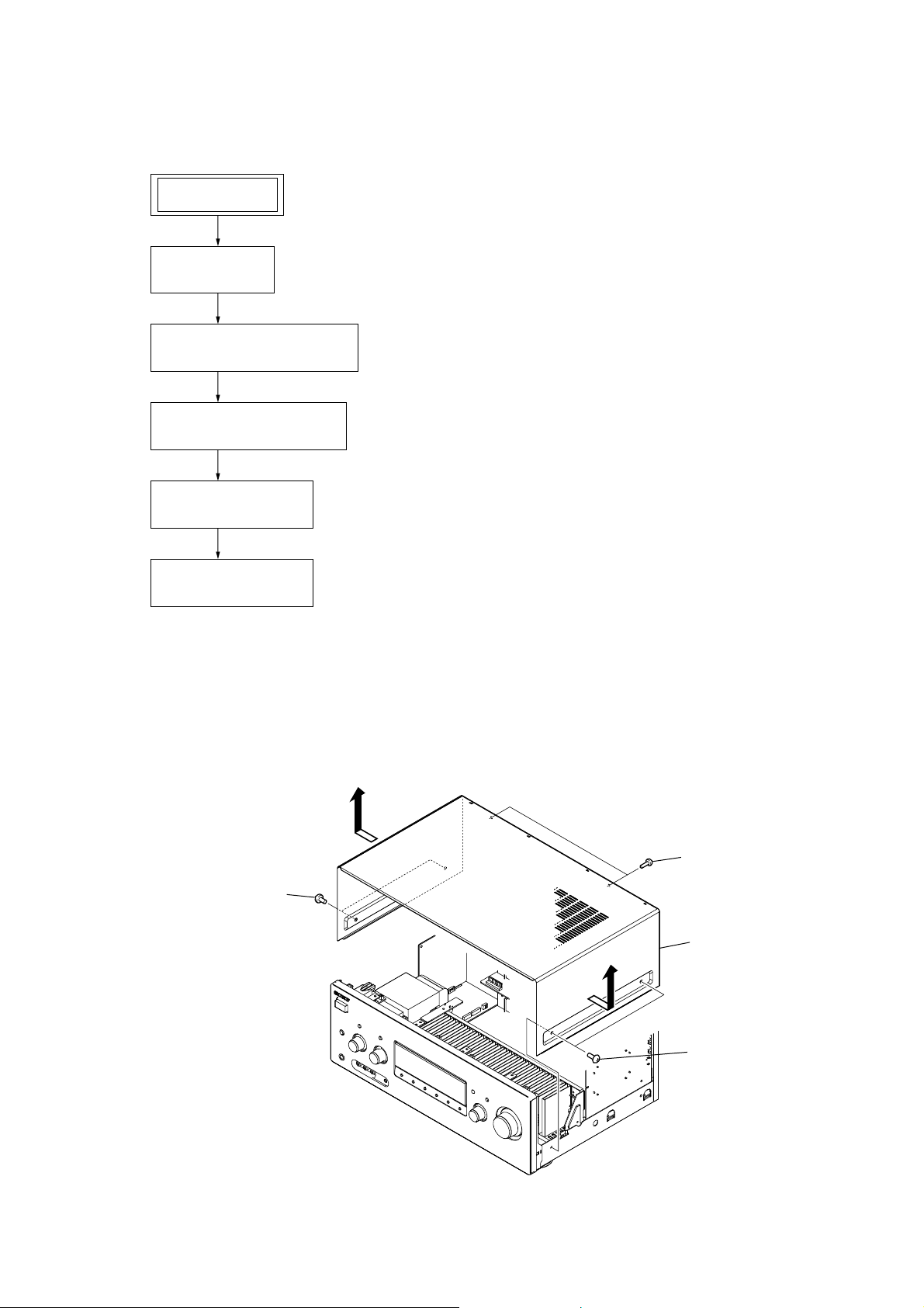
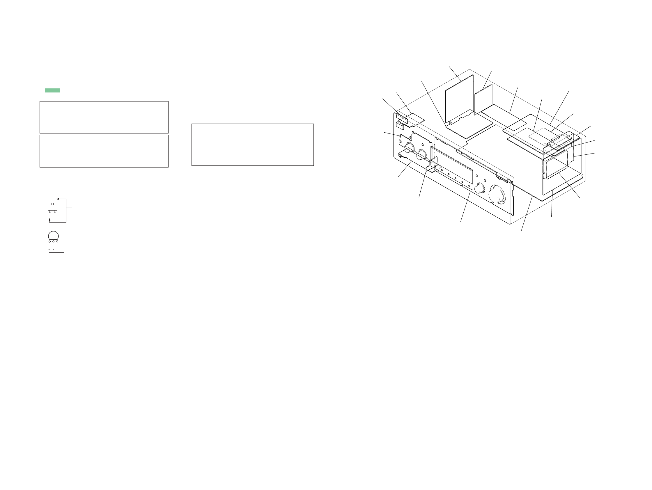
DISASSEMBLY
• This set can be disassembled in the order shown below.
3-1. DISASSEMBLY FLOW
SET
3-2. CASE
(Page 9)
3-3. FRONT PANEL BLOCK
(Page 10)
3-4. BACK PANEL BLOCK
(Page 10)
STR-DG820
SECTION 3
3-5. MAIN BLOCK
(Page 11)
3-6. MAIN BOARD
(Page 11)
Note: Follow the disassembly procedure in the numerical order given.
3-2. CASE
two screws
(BVST4 × 8 (for BLACK),
BVTT4 × 8 (for SILVER))
two screws
(BVTP3 × 8)
case
two screws
(BVST4 × 8 (for BLACK),
BVTT4 × 8 (for SILVER))
9
STR-DG820
Ver. 1.1
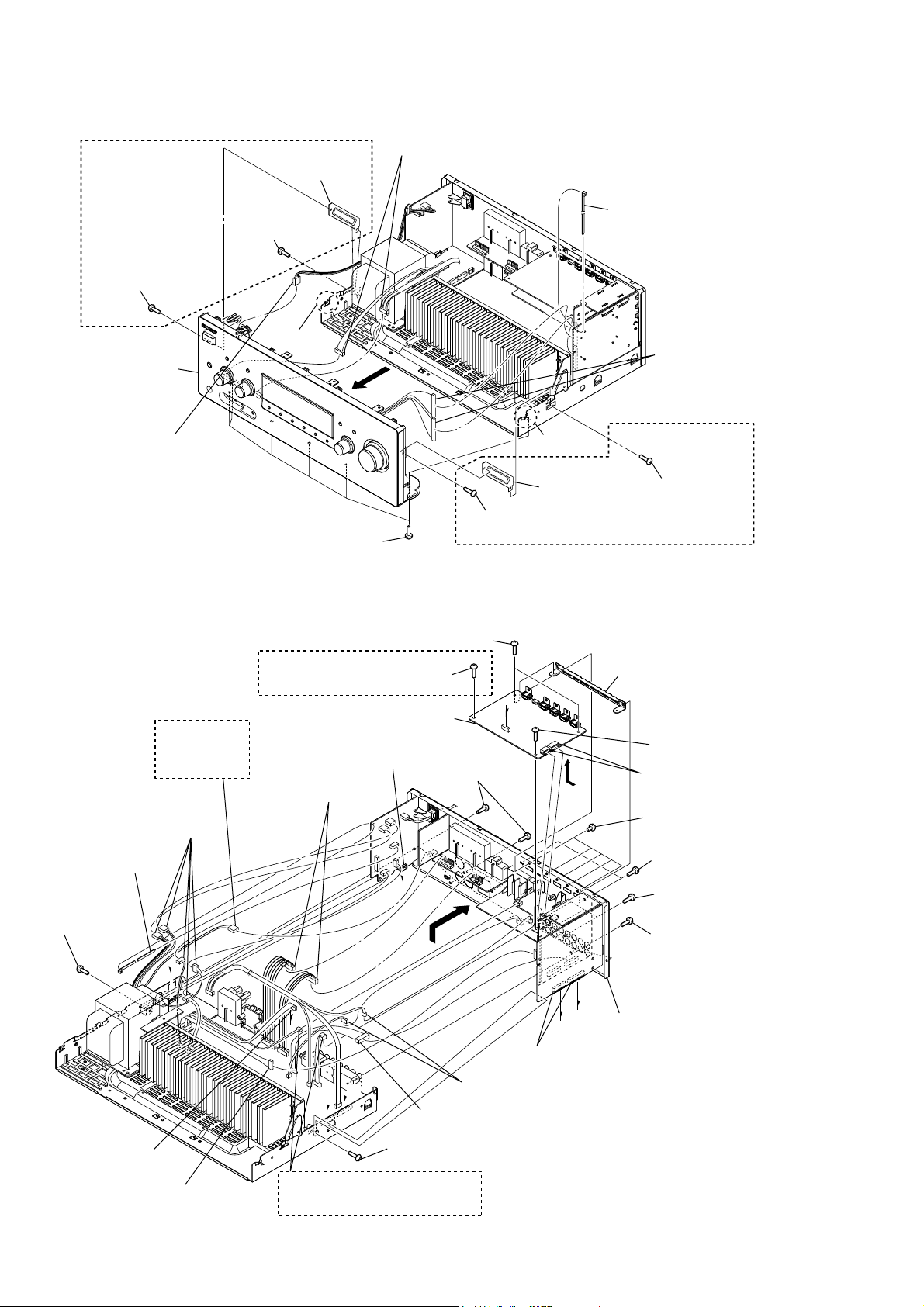
3-3. FRONT PANEL BLOCK
(AEP, ECE, UK)
screw
(BVTP3 × 8)
screw
(BVTP3 × 8)
front panel block
RB
connector
(CN1)
claw
bracket
two connectors
R
(CN721, CN725)
claw
Cut the clamp.
(CN7006, CN7007)
two connectors
• Abbreviation
ECE : Continental European, East European
and Russian models
(BVTP3 × 8)
3-4. BACK PANEL BLOCK
(AEP, ECE, UK)
(E51)
connector
XT
(CNP905)
five connectors
RI
(CN910, CN911,
CN912, CN914, CN915)
Cut the clamp.
RH
screw
RB
(BVTP3 × 8)
#
connector
(CN3507)
XB
(CN2208)
connector
two connectors
RK
(CNP285, CNP286)
"
two connectors
X
(CN102, CNP103)
six screws
RT
(CN913)
%
$
two screws
(BVTP3 × 8)
screw
(BVTP3 × 8)
HDMI board
connector
#
RM
(CN7005)
screw
R
(BVTP3 × 8)
(US, CND)
screw
(BVTP3 × 8)
eight screws
(BVTP3 × 8)
RG
two connectors
RL
(CNP203, CNP240)
connector
screw
bracket
"
%
$
two connectors
RE
(CN2222, CN2223)
• Abbreviation
CND : Canadian model
E51 : Chilean and Peruvian models
ECE : Continental European, East European
and Russian models
(BVTP3 × 8)
(AEP, ECE, UK)
HDMI bracket
screw
(BVTP3 × 8)
two connectors
(CN3003, CN3504)
five screws
(BVTT3 × 6)
two screws
(BVTP3 × 8)
three screws
(BVTP3 × 8)
screw
(BVTP3 × 8
(except AEP, ECE, UK),
BV3 × 8 CU
(AEP, ECE, UK))
back panel block
XE
10
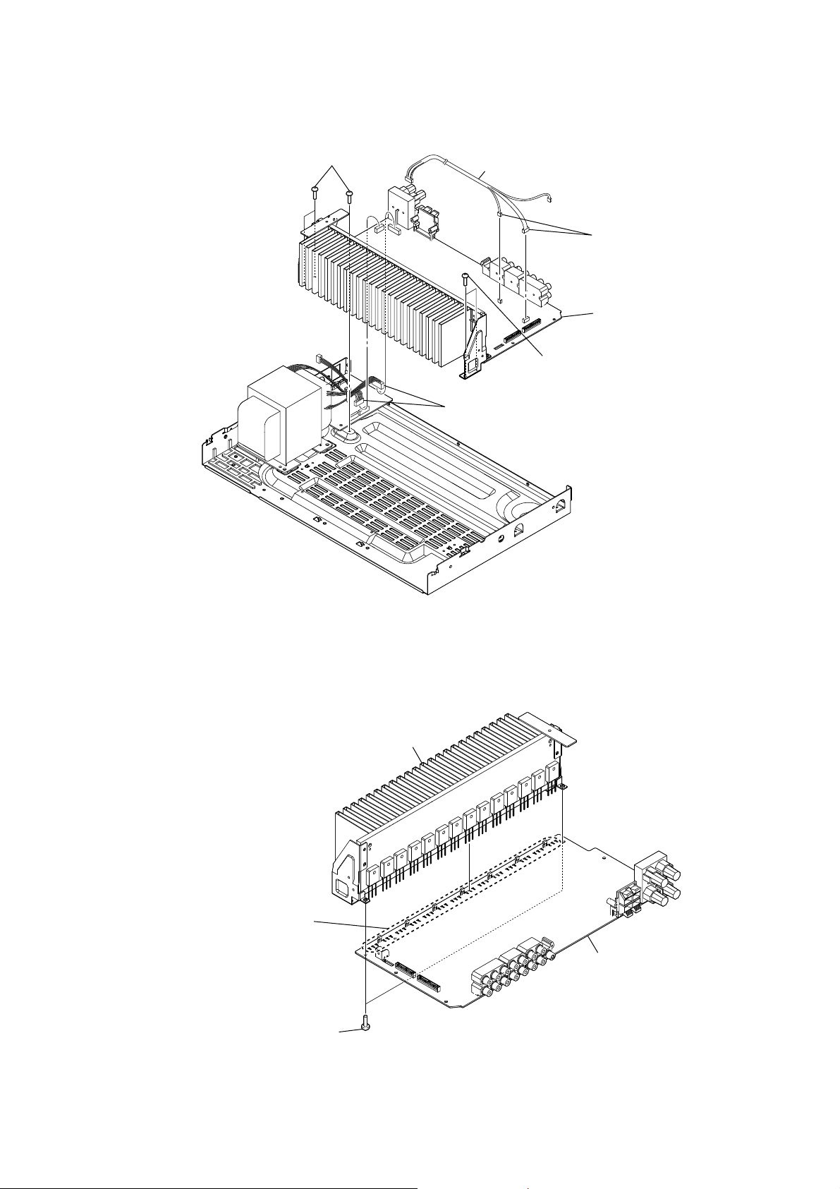
3-5. MAIN BLOCK
three screws
(BV3)
lead wire
(BV3)
two connectors
(CNP920, CNP940)
(CNP432, CNP500)
two screws
STR-DG820
two connectors
main block
3-6. MAIN BOARD
Note: This illustration sees the MAIN board from back side.
heatsink block
Remove the
forty-two solders.
two screws
(BVTP3 × 8)
MAIN board
11
STR-DG820
Ver. 1.1
SECTION 4
TEST MODE
DIGITAL MEDIA PORT TEST
Procedure:
1. Connect the DMPORT check jig (P/N: J-2501-309-A) with the
DMPORT jack (CN2226) on the DIGITAL AUDIO board.
2. While pressing the [MEMORY/ENTER] and [A.F.D.] buttons,
press the [POWER] button to turn on the main power.
3. The message “DMPORT T.” appears on the fl uorescent indica-
tor tube and enter the digital media port test mode. (Confi rma-
tion of communication line)
When “NO DETECT”, “UART NG” and “UART TO” are dis-
played on the fl uorescent indicator tube, confi rm the connec-
tion of the DMPORT check jig, and enter the mode again.
Each time the [>] button on the remote commander is
pressed, the connect check and adaptor version check are
switched.
Press the [.] button on the remote commander, connected
confi rmation of the DMPORT check jig is done again.
4. To a pinjack of the DMPORT check jig input information relevant to audio signal (sine-wave 1.0V rms) and composite video
signal (white 100% 1.0Vp-p, color bar, etc.).
5. Confi rm the output of speakers and monitor TV. (Confi rmation
of analog signal)
6. To release from this mode, press the [x] button on the remote
commander.
color
pattern
generator
oscillator
AF
J001
DIGITAL AUDIO board
CN2226
DMPORT
check jig
(Part No.:
J-2501-309-A)
VIDEO board
J210
TV
monitor
set
FL/FR
speaker
MAIN board
TB601
XM FACTORY TEST MODE
(US and Canadian models only)
Mode to confi rm operation of XM. Doing display of ID of XM
antenna and output of audio signal that XM antenna generates, it is
confi rmed that there are no problems in the communication of the
XM antenna and the tranmission of the audio signal.
Procedure:
1. The XM antenna was connected, while pressing the [TUNING
MODE] and [MOVIE] buttons, press the [POWER] button to
turn on the main power.
2. Whenever the [DISPLAY] button is pressed, the output of the
audio signal of 1 kHz L/R, 20 Hz L/R, 5 kHz L/R, muting, 1
kHz L and 1kHz R are switched.
COMMAND MODE CHANGE MODE
The command mode of the remote-commander which this set receives can be changed.
Procedure:
1. While pressing the [2CH/A. DIRECT] button, press the [POW
ER] button to turn on the main power.
2. Either the message “C.MODE AV1” or “C.MODE AV2” appears. Select the desired mode.
FLUORESCENT INDICATOR TUBE PATTERN CHECK
MODE
All fl uorescent segments are tested. When this test is activated, all
segments turn on at the same time, then each segment turns on one
after another.
Procedure:
1. While pressing the [TONE MODE] and [A.F.D.] buttons, press the
[POWER] button to turn on the main power.
2. All segments turn on.
12
MEMORY CLEARING MODE
All preset contents are cleared when this mode is activated. Use
this mode before returning the product to clients upon completion
of repair.
Procedure:
1. While pressing the [TONE MODE] and [2CH/A.DIRECT]
buttons, press the [POWER] button to turn on the main power.
2. The message “CLEARING” appears and the memories are reset to the default values.
3. When done, the message “CLEARED” appears.
SOUND FIELD CLEAR MODE
The preset sound fi eld is cleared when this mode is activated. Use
this mode before returning the product to clients upon completion
of repair.
Procedure:
1. While pressing the [MUSIC] button, press the [POWER] button to turn on the main power.
2. The message “S. F. CLEAR” appears and initialization is performed.
TUNER AM STEP CHANGE MODE
(US, Canadian, Chilean, Peruvian, Korean, Taiwan and
Australian models only)
Either the 9 kHz step or 10 kHz step can be selected for the AM
channel step.
Procedure:
1. Press the [POWER] button to turn on the main power.
2. Turn the [INPUT SELECTOR] dial to select the “AM TUNER”.
3. Press the [POWER] button to turn off the main power.
4. While pressing the [TUNING MODE] button, press the [POW
ER] button to turn on the main power.
5. Either the message “AM9k Step” or “AM10k Step” appears, select the desired step.
HISTORY MODE
The state that the set is used is memorized.
Procedure:
1. While pressing the [MEMORY/ENTER] and [MUSIC] buttons, press the [POWER] button to turn on the power and
“HISTORY” is displayed.
2. Each time the [M] [m] key of remote commander is pressed,
the item is switched in order as follows.
Items Display
Protector count COUNT XX
Total single power on time S xxHxxM
Sound fi eld xxxxxxxxxx
Input function xxxxxxxxxx
Input mode xxxxxxxxxx
Digital select xxxxxxxxxx
Stream information xxxxxxxxxx
Signal confi guration CONF xxxxx
Headphones HEADPH xxx
Volume VOL xxx
Bass BASS xxdB
Treble TREB xxdB
Level FL/FR FL/R xx xx
Level SL/SR SL/R xx xx
Level CT/SW C/SW xx xx
Level BL/BR BL/R xx xx
Total power on time T xxHxxM
Muting MUTING xxx
Power on counter
(Rebox test mode)
REBOX xx
SECTION 5
ELECTRICAL CHECK
STR-DG820
SPECIAL MENU MODE
Procedure:
1. Press the [POWER] button to turn on the main power, then while pressing the [TONE MODE] button, press the [A.F.D.], [2CH/A.
DIRECT], [MUSIC], [MOVIE] button in order, the message “SPECIALIZE” appears.
2. Press the [M] [m] button on the remote commander, the message “< SPECIAL>” appears.
3. Press the [,] button on the remote commander, the item is appears.
4. Each time the [M] [m] button on the remote commander is pressed, the item is switched in order as follows.
Some items can change the content. Display the cursor by pressing the [,] button on the remote commander, and changing the content
by pressing the [M] [m] button on the remote commander, and fi x the content by pressing the [<] button on the remote commander
when you want to change the content of the item.
5. To release from this mode, while pressing the [TONE MODE] button, press the [A.F.D.], [2CH/A. DIRECT], [MUSIC], [MOVIE] button in order again, the message “OFF” appears.
Items Display Remark
When [,] button on the remote commander is pressed, the message “G82
Model/Destination change MODEL
Main micom version display M.Ver X.XX X.XX: System controller software version
HDMI mico mversion display H.Ver X.XX X.XX: HDMI controller software version
DSP serial fl ash version display S.Ver X.XX
HD update HD UPDATE
HDCP key read HDCP KEY
Auto cal mic test SP OUT
FL display fonts test FL FONT
FL display test All segments turn on
DSP halt DSP HALT
Super reset RESET
RAM watch menu RAM WATCH
EEPROM debug EEPROM
Protector on/off PROTECTOR
Audio swap SWAP MODE
Volume value display (FL/FR) F****RXXXX
Volume value display (SL/SR) S****AXXXX
Volume value display (CT/SW) C****WXXXX
Volume value display
(SBL/SBR)
DAC mute information disclosure 1 U XXXXXXXX
DAC mute information disclosure 2 L XXXXXXXX
FL display duty change DUTY
B****BXXXX
** XXX” is appears
**: Destination
XXX: FIX or AUT
X.XX: Serial fl ash software version
When [,] button on the remote commander is pressed, the message “ON”
or “OFF” is appears
When [,] button on the remote commander is pressed, the message “ON”
or “OFF” is appears
When [,] button on the remote commander is pressed, the message
“SOURCE” or “mic” is appears
SOURCE: normal mode, MIC: mode that output audio from mic input
When [,] button on the remote commander is pressed, the message
“0X**=X” is appears
**: 20 to FF, X: character
Each time [DISPLAY] button to change as follows
all on t test pattern 1 t test pattern 2 t all off t all on
When [,] button on the remote commander is pressed, the message “ON”
or “OFF” is appears
Not used for the servicing
When EEPROM initialization is required, perform the “memory clearing
mode”
When [,] button on the remote commander is pressed, the message
“XXXXXXXXXX” is appears
XXXXXXXXXX: Various internal RAM(Switching with [M] [m] button on the
remote commander)
When [,] button on the remote commander is pressed, the message “****
XX” is appears
****: EEPROM address, XX: EEPROM data
When [,] button on the remote commande is pressed, the message “ON”
or “OFF” is appears
When [,] button on the remote commander is pressed, the message
“XXXXXXXXXX” is appears
XXXXXXXXXX: audio swap mode
Switching with [M] [m] button on the remote commander
****: Front L-ch volume value, XXXX: Front R-ch volume value (for design
evaluation)
****: Surround L-ch volume value, XXXX: Surround R-ch volume value (for
design evaluation)
****: Center volume value, XXXX: Sub woofer volume value (for design
evaluation)
****: Surround back L-ch volume value, XXXX: Surround back R-ch volume
value (for design evaluation)
Display of module information to demand muting in system controller (for
design evaluation)
Display of module information to demand muting in system controller (for
design evaluation)
When [,] button on the remote commander is pressed, the message “XXX”
is appears
XXX: Duty value of FL display (1% to 100%) (for design evaluation)
FM AUTO STOP CHECK
signal
generator
set
Procedure:
1. Turn on the set.
2. Input the following signal from signal generator to FM antenna
input directly.
Carrier frequency : A = 87.5 MHz, B = 98 MHz, C = 108 MHz
Deviation : 75 kHz
Modulation : 1 kHz
ANT input : 1 kHz
Note: Use 75 ohm coaxial cable to connect signal generator and the set.
You cannot use video cable for checking.
Use signal generator whose output impedance is 75 ohm.
3. Set to FM tuner function and scan the input FM signal with
automatic scanning.
4. Confi rm that input frequency of A, B and C are detected and
automatic scanning stops.
When the station signal is received in good condition, automatic
scanning stops.
STR-DG820
1313
STR-DG820
STR-DG820
1414
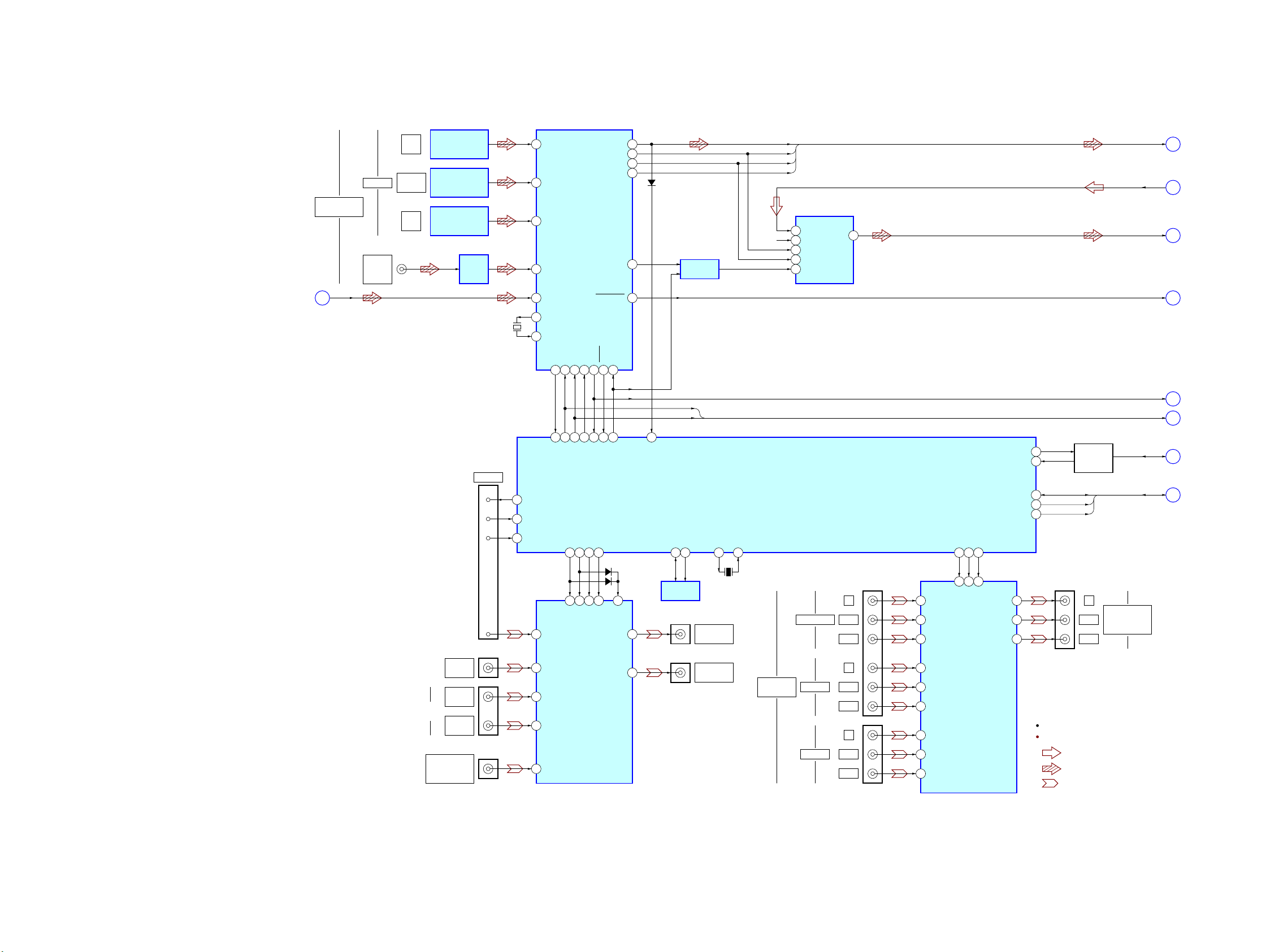
SYSTEM CONTROLLER
IC7001 (1/4)
DIGITAL OPTICAL
RECEIVER
IC2201
TV
IN
SCHMITT
TRIGGER
IC2239
DIGITAL AUDIO
INTERFACE RECEIVER
IC2208
J2001
COAXIAL
DVD
IN
A/D CONVERTER
IC2233
D2203
RX0 RDATA
CEC DATA
SWITCH
Q7001 – 7004
VIDEO AMP
IC210
DIGITAL OPTICAL
RECEIVER
IC2202
VIDEO 1
IN
VIDEO 2 IN/
PORTABLE AV IN
VIDEO
DVD
VIDEO IN
SAT
VIDEO IN
DIGITAL OPTICAL
RECEIVER
IC2204
SAT
IN
OPTICAL
VIDEO 1 IN
DVD IN
J211
(1/2)
DIGITAL
(ASSIGNABLE)
COMPONENT
VIDEO
2 21
XMCK
DIR_DO
R-CH
27
DOUT
9
RBCK
DIR_BCK
17
BCK
8
VINL
13
VINR
14
LRCK
7
SCKI
6
RLRCK
DIR_LRCK
20
RMCK
DIR_MCK
16
SI_A
SI_A, DIR_BCK,
DIR_LRCK, DIR_MCK
L_OUT
SI_B
RX2
4
RX3
5
RX4
8
VIN3
7 1
DMPORT_RX
141
CH1 IN1
1
CH2 IN1
8
CH3 IN1
17
CH1 IN2
3
CH2 IN2
10
CH3 IN2
15
VIN1
9
RX6/UI
10
XIN
DO
29
37
COMPOSITE_SW1
160
80
SW1
14
COMPONENT_SW1
165
SW1
2
COMPONENT_SW2
166
SW1
4
VMUTE
167
PS
23
COMPOSITE_SW2
159
SW2
10
COMPOSITE_SW3
158
SW3
4
COMPOSITE_SW4
157
X1_(CLOCK_OUT)
40
EEPROM_SDA
174
EEPROM_SCL
175
X0_(CLOCK_IN)
39
SW46SW5
VOUT1
2
DIR_ERROR REER
36
79
DIR_CKST CKST
34
78
DIR_DATA0
77
COM1_DATA DI
38
81
COM1_CLK CL
40
83
DIR_CE CE
39
82
DIR_XMODE XMODE
41
84
XOUT
28
A
SPDIF
SWITCHING
IC2234
B
AUDIO /VO
33
DIR_NON_AUDIO
E
DIR_ERROR
F
COM1_DATA, COM1_CLKCOM1_CLK
COM1_DATA
G
CEC
H
SDA, SCL
HDMI_RESET
J
D
C
X2201
24.576MHz
D211
D210
VIN5
3
VIN4
VIN2
5
CN2226 (1/2)
17
DMPORT_VIDEO
5
DMPORT_RX
DMPORT_TX
140
6
DMPORT_TX
DMPORT_DET
76
7
DET
DMPORT
J703 (1/2)
VIDEO 1
VIDEO IN
13
24
CH1 OUT
101
CEC_IN
117
HDMI_SDA
SDA
SCL
HDMI_RESET
118
HDMI_SCL
65
HDMI_UCOM_RST
120
CEC_OUT
22
CH2 OUT
20
CH3 OUT
J210 (1/2)
MONITOR
VIDEO OUT
J210 (2/2)
15
VOUT2
VIDEO 1
VIDEO OUT
J211 (2/2)
Y
P
B/CB
PB/CB
Y
P
B/CB
PB/CB
SAT IN
CH1 IN3
5
CH2 IN3
12
CH3 IN3
13
Y
P
B/CB
PB/CB
Y
P
B/CB
PB/CB
J220 (1/2) J220 (2/2)
J221
COMPONENT
VIDEO
MONITOR OUT
VIDEO AMP
IC220
X7001
4MHz
EEPROM
IC7005
:VIDEO
: AUDIO (ANALOG)
: AUDIO (DIGITAL)
SIGNAL PATH
R-ch is omitted due to same as L-ch.
6-1. BLOCK DIAGRAM - MAIN Section -
SECTION 6
DIAGRAMS
(Page 15)
(Page 16)
(Page 16)
(Page 16)
(Page 16)
(Page 15)
(Page 15)
(Page 17)
(Page 16)
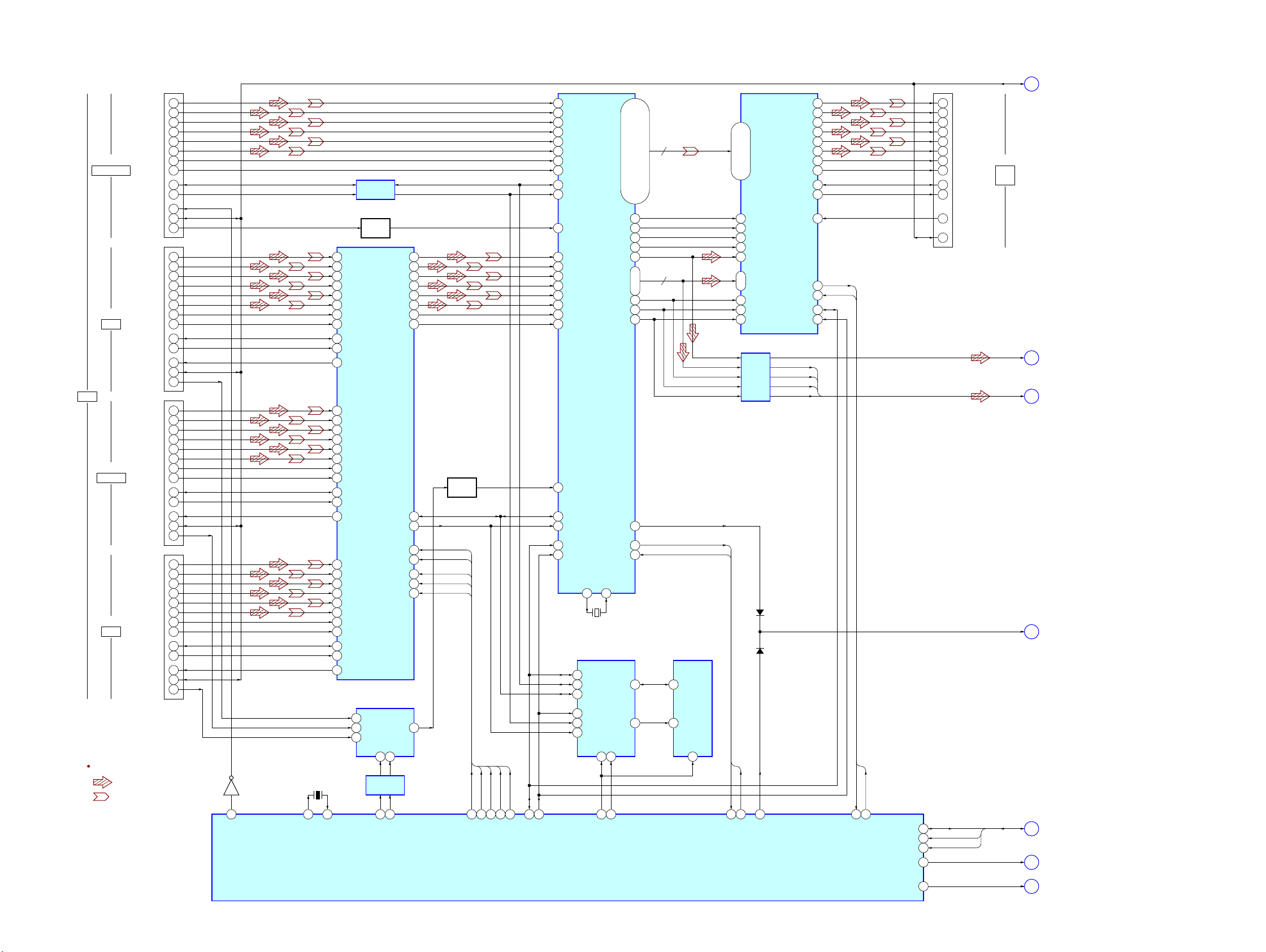
STR-DG820
STR-DG820
1515
CN3500
SAT IN
ADT0P YDT0P52 31
YDT0N
32
YDT1P
28
YDT1N
29
YDT2P
25
YDT2N
26
YCLKP
34
YCLKN
35
ADT0N51
7DATA0+
HDMI INPUT
SELECTOR
IC3501
HDMI
RECEIVER
IC3506
9DATA0–
ADT1P
55
ADT1N
54
4DATA1+
6DATA1–
ADT2P
58
ADT2N
57
1DATA2+
3DATA2–
ACLKP
49
ACLKN
48
10CLOCK+
12CLOCK–
SDA_A
45
SCL_A
46
16SDA (5V)
15SCL (5V)
HPD_A
4419HOT PLUG DET
13CEC
18+5V POWER
CN3503
VIDEO 1 IN
7DATA0+
9DATA0–
4DATA1+
6DATA1–
1DATA2+
3DATA2–
10CLOCK+
12CLOCK–
16SDA (5V)
15SCL (5V)
19HOT PLUG DET
13CEC
18+5V POWER
7DATA0+
9DATA0–
4DATA1+
6DATA1–
1DATA2+
3DATA2–
10 CLOCK+
12 CLOCK–
16 SDA (5V)
15 SCL (5V)
19 HOT PLUG DET
13 CEC
CN3505
HDMI
OUT
CN3501
DVD IN
BDT0P
71
BDT0N
70
7DATA0+
9DATA0–
BDT1P
74
BDT1N
73
4DATA1+
6DATA1–
BDT2P
77
BDT2N
76
1DATA2+
3DATA2–
R0X0+
44
HSYNC
20 HSYNC2
VSYNC
21 VSYNC3
ODCK
5 IDCK88
DE
19 DE1
SPDIF
78
SPDIF
SD0 – SD3
BCK
LRCK
MCK
A
MUTE
(HDMI_ERROR)
L
SDA, SCL,
HDMI_RESET
J
SD0 – SD3, BCK,
LRCK, MCK
K
SPDIF4
SCK 86 SCK11
WS CSDA
85 WS10 49
CSCL
48MCLK 89 MCLK5
R0X0–
43
R0X1+
48
R0X1–
47
R0X2+
52
R0X2–
51
R0XC+
40
R0XC–
39
DSDA0
33
DSCL0
34
R1X0+
62
R1X0–
61
R1X1+
66
R1X1–
65
R1X2+
70
R1X2–
69
R1XC+
58
R1XC–
57
DSDA128
DSCL1
R1PWR5V
Q0 – Q35
SD0 – SD3
SD0 – SD3
D0 – D35
27
30
SDA_SINK
39
SCL_SINK
38
CSDA
26
CSCL
27
D3000
D3001
OUTDIS 42
HPD_SINK
40
SELA
1444_SELA
1444_SELB
1444_SELC
23
SELB
22
SELC
21
TX0+
34
TX0–
33
TX1+
37
TX1–
36
TX2+
40
TX2–
39
TXC+
31
TXC–
30
DSDA 47
DSCL
46
HPD
51
BCLKP
68
BCLKN
67
10CLOCK+
12CLOCK–
SDA_B63
SCL_B
64
16SDA (5V)
15SCL (5V)
HPD_B6219HOT PLUG DET
13CEC
18+5V POWER
HDMI
CN3502
BD IN
CDT0P9
CDT0N
8
7DATA0+
9DATA0–
CDT1P
12
CDT1N
11
4DATA1+
6DATA1–
CDT2P
15
CDT2N
14
1DATA2+
3DATA2–
CCLKP
6
CCLKN
5
10CLOCK+
12CLOCK–
SDA_C2
SCL_C
3
16SDA (5V)
15SCL (5V)
HPD_C8019HOT PLUG DET
CEC
H
13CEC
18+5V POWER
LEVEL SHIFT
IC3502
SWITCH
Q3501
R0PWR5V
35
SWITCH
Q3500
2Y15
2Y2 2-COM
P5V_SELA
XOUT
XIN
P5V_SELB
2 3
2Y3
4
10
SIGNAL SELECTOR
IC3503
A
9
55
HPD_IN1
Q3505
22 56
1444_SELA
51
1444_SELB
52
1444_SELC
1444_OEB
1444_HPD
53
B
EDID_SELA
EDID_SELB
A
35 36
CSDA
CSCL
28 27
B
INVERTER
IC3513
1444_OEB
1444_HPD
54 21
INT
102
MUTEOUT
75
RESET# 100
RX_INT
RX_RST
RX_INT
RX_RST
20 19
MUTE
65
INT
24
RESET#
25
TX_INT
TX_RST
TX_INT
TX_RST
43 42
2Y01
1Y0
12
2Y3
4
1Y3
11
SDA5
SCL
6
2Y15
1Y1
14
2-COM
3
1-COM
13
VUCOM_SDA
SDA
SCL
HDMI_RESET
33
NON_LPCM
M
NON_LPCM 64
TX_5VPWR
N
TX_5VPWR 41
VUCOM_SCL
34
RESET
10
DATA SELECTOR
IC3504
EEPROM
IC3505
10 9
AB WP
7
XTALOUT94XTALIN
95
X3500
28.322MHz
16 – 13, 10 –7, 3 – 1, 144,
141 – 138, 135 –132, 129 – 126,
123 – 120, 117 –114, 111 – 108,
98 – 90, 86 – 77,
75 – 67, 63 – 56
36
4
81 – 84
9 – 6
BUFFER
IC3507
1311
X3000
10MHz
HDMI
TRANSCEIVER
IC3508
HDMI CONTROLLER
IC3000
:VIDEO
: AUDIO (DIGITAL)
SIGNAL PATH
6-2. BLOCK DIAGRAM - HDMI Section -
(Page 14)
(Page 14)
(Page 16)
(Page 16)
(Page 14)
(Page 16)
(Page 18)
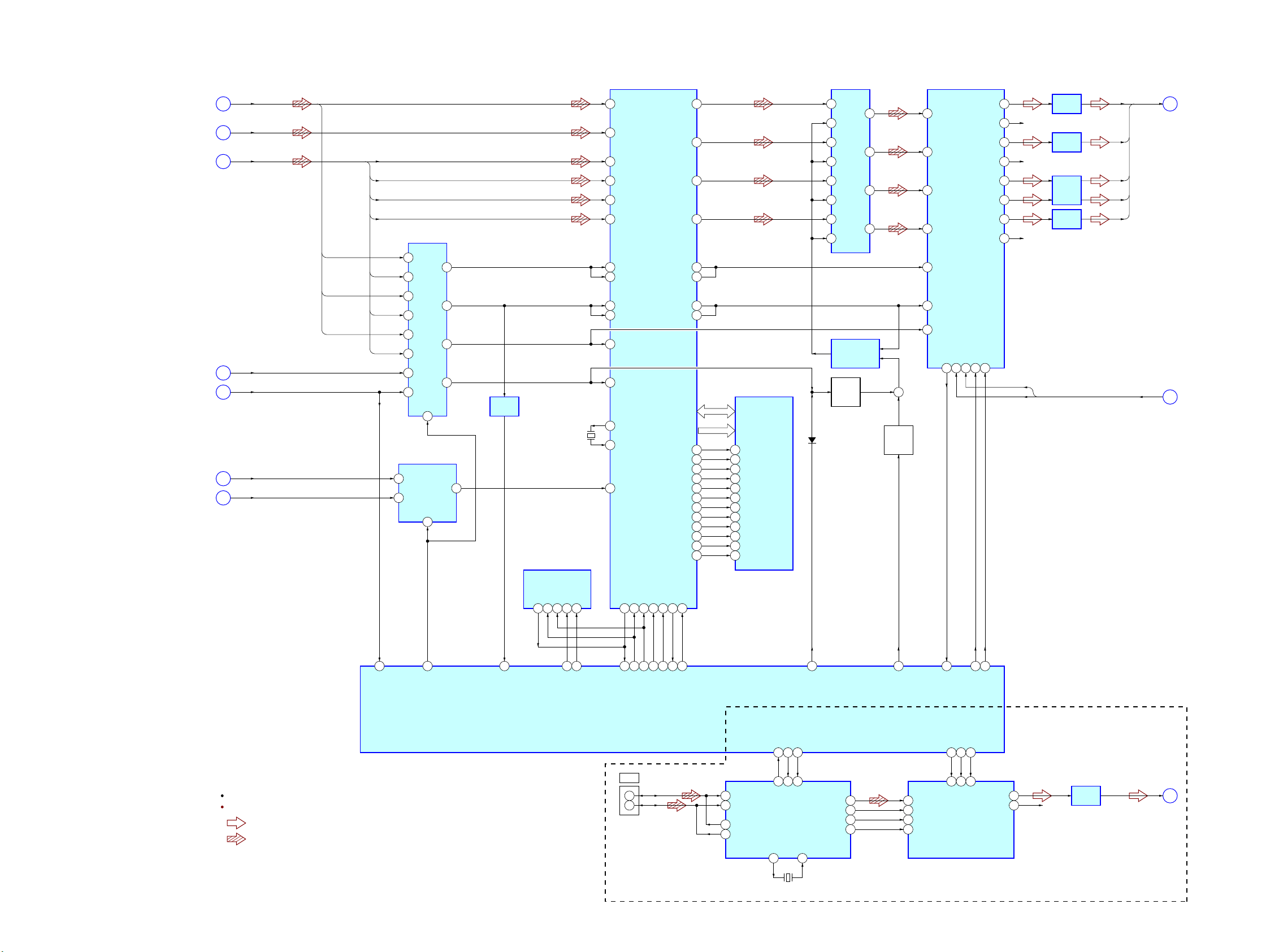
STR-DG820
STR-DG820
1616
DIR_BCK
DIR_LRCK
DIR_MCK
SI_A
SI_A, DIR_BCK,
DIR_LRCK, DIR_MCK
B
BCK
SD1
LRCK
MCK
SD0
SD0 – SD3, BCK,
LRCK, MCK
K
SI_B
D
DIR_ERROR
F
DIR_NON_AUDIO
E
NON_LPCM
M
MUTE
(HDMI_ERROR)
L
SIGNAL SELECTOR
IC2212
SIGNAL SELECTOR
IC2236
A3
14
DSP
IC5021
AXR0[10]
/AXR1[3]
B8
AXR0[11]
/AXR1[2]
A8
AXR0[12]
/AXR1[1]
B7
ACLKR0
A5
ACLKR1
E1
AXR0[13]
/AXR1[0]
B6
SD2
AXR0[14]
/AXR2[1]
A6
SD3
AXR0[15]
/AXR2[0]
AHCLKX0/
AHCLKX2
B5
B3
Y3
13
12
AXR0[0]
A14
AXR0[1]
B13
AXR0[2]
A13
AXR0[3]
B12
ACLKX0
A4
ACLKX1
E2
AFSR0
B4
AFSX2
C11
AFSR2
SPI0_SOMI
C12
Y2
9
A2
11
B2
10
A1
5
B1
6
AFSR1
F1
C2
Y1
7
A0
2
B0
3
1
Y0
SELECT
4
MUTING
IC2232
B2
9
A2
Y2
10
8
Y3
11
B3
12
A3
13
B1
5
A1
4
Y1
6
B0
2
A0
1
D/A CONVERTER
IC2238
DATA1
45
DATA2
R-CH
46
DATA3
47
DATA4
31
Y0
3
CH0
7
CH1
6
5
COMMON
A
2SO5SI6
SCK1CE#
1
BUFFER
IC2211
90
HDMI/DIR
SELECT
64
HDMI_ERROR
(MUTE)
169
FSRATE
137
B14
SPI0_MISO
SPI0_SIMO
138
B15
SPI0_MOSI
SPI0_CLK
139
C16
SPI0_CLK
SPI0_SCS#
95
C15
SPI0_CS#
92
SFLASH_CE#
7
HOLD#
33
MDO34MDI35MC36ML37RST
91
SFLASH_HOLD#
SPI0_ENA#
93
D16
SPI0_ENA#
ACLKX2
163
D11
SPI0_INT
69
DA_MD0
75
DAC_MUTE
72
DIGI/ANA
70
DA_LATCH
71
DA_RESET
COM1_DATA, COM1_CLKCOM1_CLK
COM1_DATA
G
XML
Q
RESET#
94
G2
DSP_RESET
3+D
2ÐD
J101
XM
COMRXP
18
DATA∗
2
BCK
R-CH
1
LRCK
3
SCK
16
COMRXM
19
COMTXP
23
COMTXM
22
XM_MIXMO
3
148
SCTXOUT
XM_MOXMI
5
149
SRCXIN
XM_RESET
OSCOUT26OSCIN
28
X101
45.1584MHz
11
150
RESET∗
XM_DAC_MDI
13
144
MD(MDI)
XM_DAC_MC
14
143
MC
XM_DAC_MS
15
142
ML(MS)
XM RECEIVER
IC102
D/A CONVERTER
IC105
I2SDATA
37
VOUTL
7
VOUTR
8
I2SSCLK
39
I2SLRCLK
41
I2SOCLK
43
LINE AMP
IC104
SERIAL FLASH
IC5020
MUTING
CONTROLLER
IC2226
BCK
40
AFSX0
A3
AFSX1
EM_D[0] –
EM_D[31]
F2
EM_CLK
R14
LRCK
41
SCKI
38
VOUT3
12
VOUT4
11
LINE AMP
IC2220
VOUT5
C
SL
10
VOUT6
9
LINE AMP
IC2221
R-CH
VOUT1
14
VOUT2
13
LINE AMP
IC2222
R-CH
VOUT7
16
VOUT8
20
LINE AMP
IC2219
SW
FL
SBL
FL, SL, C,
SW, FBL
P
+
MUTING
SWITCH
Q2205
MUTING
SWITCH
Q2206
SD-RAM
IC5022
CLK
DQ0 – DQ31
EM_A[0] –
EM_A[10]
A0 – A10
68
EM_CKE
T14
CKE
67
EM_CS[0]#
F15
CS#
20
EM_RAS#
F16
RAS#
19
EM_CAS#
R3
CAS#
18
EM_WE#
T3
WE#
17
EM_BA[0]
G15
BA0
22
EM_BA[1]
H16
BA1
23
EM_DQM[0]
R4
DQM0
16
EM_DQM[1]
T13
DQM1
71
EM_DQM[2]
P13
DQM2
28
EM_DQM[3]
R15
DQM3
59
D2201
SYSTEM CONTROLLER
IC7001 (2/4)
OSCIN
J2
OSCOUT
J3
X002
25MHz
: AUDIO (ANALOG)
: AUDIO (DIGITAL)
SIGNAL PATH
R-ch is omitted due to same as L-ch.
(US, Canadian)
6-3. BLOCK DIAGRAM - DSP/XM Section -
(Page 14)
(Page 14)
(Page 15)
(Page 14)
(Page 15)
(Page 14)
(Page 17)
(Page 17)
(Page 15)
(Page 14)
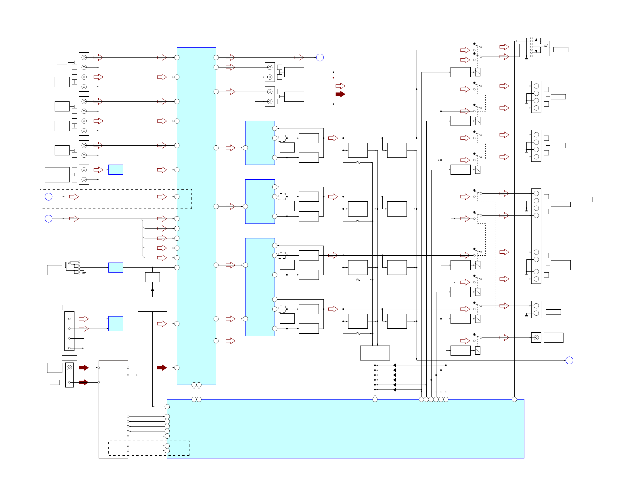
STR-DG820
STR-DG820
1717
6-4. BLOCK DIAGRAM - AUDIO Section -
L
TV IN
R
L
SA-CD/CD
CD-R IN
DVD
AUDIO IN
R
L
SA-CD/CD
CD-R OUT
R
J401
(1/2)
R-CH
R-CH
R-CH
L
R
L
SAT
AUDIO IN
R
J403
J404 (1/2)
J401 (2/2)
R-CH
R-CH
VIDEO 1
AUDIO IN
L
R
L
R
R-CH
J703 (2/2)
Q
XML
VIDEO 2 IN
PORTABLE AV IN
AUDIO
L
R
R-CH
P
FL, SL, C,
SW, FBL
SBL
SL
FL
C
SW
LINE AMP
IC706
MIC AMP
IC705
MIX AMP
IC3002
INL9
RECL1
47
29
LOUT
76
L
VIDEO 1
AUDIO OUT
R
R-CH
J404 (2/2)
RECL2
27
FLOUT
14
+VOUT1
2
NF1
5
INL7
51
INL12
41
INL11
43
IN1
6
INL13
38
INL0
47
INL15
34
LIN
72
SLIN
68
SBLIN
66
CIN
70
SWIN
71
INL1 (TUNER_L)
DATA
63
10
67
CN2226 (2/2)
13
L+
11
L–
14
R+
12
R–
DMPORT
TUNER (FM/AM)
AM
INL2
(DMPORT_L)
61
INL3
59
FM ANT
AM ANT
L CH
R CH
DO
R-CH
R-CH
R-CH
RDS_DATA
RDS_INT
DI
CLK
CE
FM75Ω
COAXIAL
ANTENNA
105 TUN_DO
8 MIC_MUTE
SD
EVOL_DATA
CLK
11
66
EVOL_CLK
68
PROTECTOR
25
SW_PREOUT_RY
34
HP_DET
27
C. SL. SBL_RY
23
SBR_RY
26
SP A/B_RY
24
SP A_RY
32
HP_RY
109 T U N _ S D
104 R D S _ D A TA
164 RDS_INT
107 TUN_DATA
106 TUN_CLK
108 TUN_CE
(AEP, ECE, UK)
MUTING
Q713
MUTING
CONTROL SWITCH
Q712, 714
D709
J701
AUTO
CAL MIC
SYSTEM CONTROLLER
IC7001 (3/4)
INPUT SELECTOR,
ELECTRICAL VOLUME
IC400
–VOUT1
3
BIAS
Q701, 702
BOOSTER
Q703
BOOSTER
Q704
CURRENT
DETECT
Q711, 712
POWER_DETECT
R
L_OUT
C
AF POWER
SENSOR
Q720
POWER AMP
IC700
SLOUT
18
+VOUT1
2
NF1
5
IN1
6
–VOUT1
3
BIAS
Q801, 802
BOOSTER
Q803
BOOSTER
Q804
CURRENT
DETECT
Q811, 812
AF POWER
SENSOR
Q820
POWER AMP
IC800
SBL OUT
20
+VOUT1
2
NF1
5
IN1
6
–VOUT1
3
BIAS
Q601, 602
BOOSTER
Q603
BOOSTER
Q604
CURRENT
DETECT
Q611, 612
AF POWER
SENSOR
Q620
POWER AMP
IC600
COUT
16
SWOUT
15
+VOUT2
12
NF2
9
IN2
8
–VOUT2
11
BIAS
Q651, 652
BOOSTER
Q653
BOOSTER
Q654
CURRENT
DETECT
Q661, 662
AF POWER
SENSOR
Q670
AF POWER
PROTECTOR
Q320, 321, 323 – 325
RY301
RELAY DRIVE
Q301
RY355
RELAY DRIVE
Q355
RY360
RELAY DRIVE
Q360
RY365
RELAY DRIVE
Q365
RY350
RELAY DRIVE
Q350
RY375
RELAY DRIVE
Q375
RY370
RELAY DRIVE
Q370
D7007
D7002
D7009
D7005
D7008
D7004
SUBWOOFER
AUDIO OUT
J405
CENTER
TB001
+
–
+
–
+
–
SURROUND
BACK
R-CH
L
R
TM2880
+
–
+
–
SURROUND
L
R
TB603
+
–
–
FRONT B
R-CH
R-CH
–1
–1
–2
–2
–1
–2
–2
–1
+
L
R
TB601
J702
–2
–1
+
–
–
FRONT A
PHONES
SPEAKERS
+
: AUDIO (ANALOG)
: TUNER
SIGNAL PATH
R-ch is omitted due to same as L-ch.
(US, Canadian)
(EXCEPT AEP, ECE, UK)
Abbreviation
: Continental European, East European
and Russian models
ECE
(EXCEPT AEP, ECE, UK)
(EXCEPT AEP, ECE, UK)
(EXCEPT AEP, ECE, UK)
(Page 16)
(Page 16)
(Page 14)
(Page 18)
Ver. 1.1
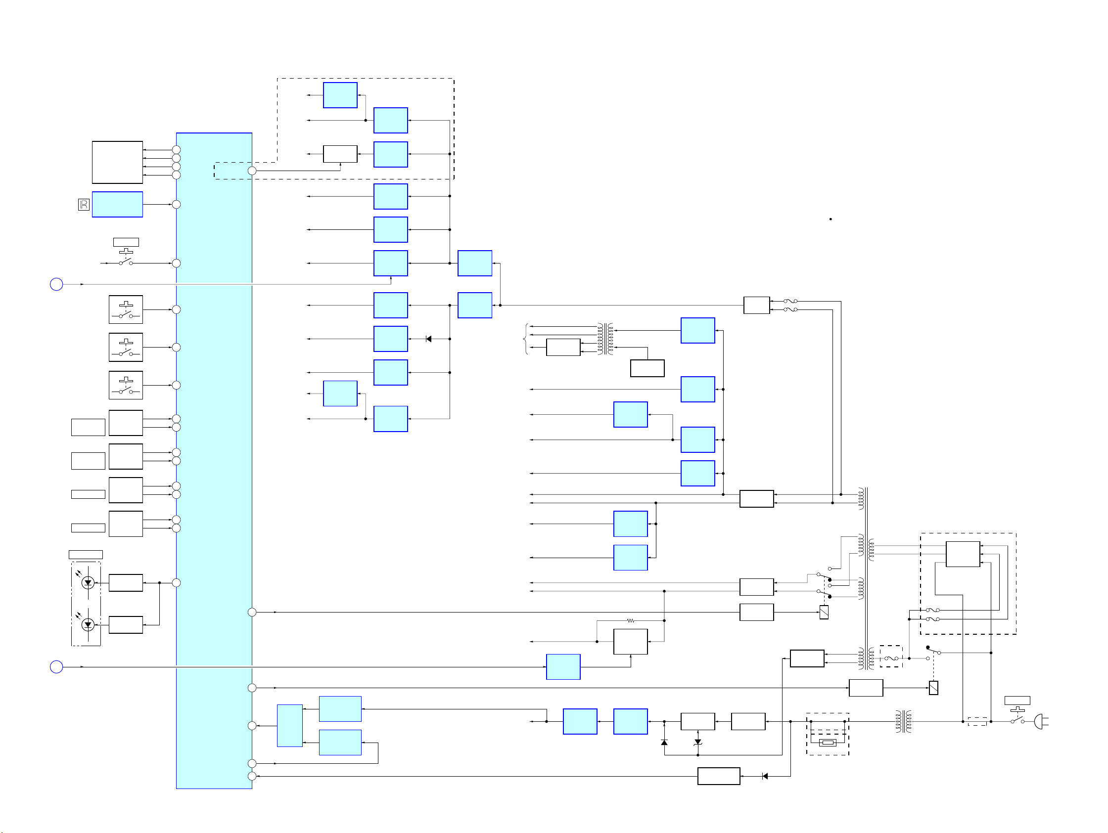
STR-DG820
STR-DG820
1818
RY910
RY920
RELAY DRIVE
Q911
RELAY DRIVE
Q920
ND701
FLUORESCENT
INDICATOR TUBE
SYSTEM CONTROLLER
IC7001 (4/4)
FL_DATA
155
FL_CLK
156
FL_LATCH
154
FL_BK
153
REMOTE CONTROL
RECEIVER
IC701
119 SIRCS-IN
2 POW-SW_DETSTBY +3.3V
98 AD-KEY1
SW1 (1/2)
POWER
S711, 712
99 AD-KEY2
S701 – 705
100 AD-KEY3
S113 – 115,
S708
16 FUNC1
15 FUNC2
ROTARY
ENCODER
INPUT
SELECTOR
S715
10 VOL1
9VOL2
ROTARY
ENCODER
MASTER
VOLUME
S722
18 TUNE1
17 TUNE2
ROTARY
ENCODER
– TUNING +
RV103
20 TONE1
19 TONE2
3 LED_STDBY
LED DRIVE
Q709, 710
LED DRIVE
Q701, 711
ROTARY
ENCODER
– TONE +
RV104
ON/STANDBY
D701
(GRN)
(RED)
(AC IN)
SW1 (2/2)
POWER
T910 (US, CND, E51, TW)
T911 (AEP, ECE, UK, KR, AUS)
SUB POWER
TRANSFORMER
171POW_RY
22BRIDGABLE_RELAY
145XM_POWER
126RST_TRG
170STOP
131INTIX
TH910
(US, CND, TW)
(EXCEPT E51)
(AEP, ECE, UK, E51, KR, AUS)
D919, 920
D3511, 3512
AC OFF DETECT
Q910
RECT
D915 – 918
RECT
D940 – 943
REGULATOR
Q912 – 914
D922D914
+5V
REGULATOR
IC910
–5V
REGULATOR
IC202
OVER LOAD
DETECTOR
IC565
LIMITER
SWITCH
Q500, 501
+3.3V
REGULATOR
IC7006
RESET SIGNAL
GENERATOR
IC7003
RESET
SWITCH
IC7002
RESET SIGNAL
BUFFER
IC7004
STBY +3.3V
POWER AMP B–
B+
B–
F910
VIDEO –5V
+9V
REGULATOR
IC7007
TUNER +9V
FOR FLUORESCENT
INDICATOR TUBE
RECT
D704 – 707
OSC
Q705, 706
T701
DC/DC
TRANSFORMER
+5V
REGULATOR
IC201
+12V
REGULATOR
IC708
VIDEO +5V
HDMI +3.3V
+7V
REGULATOR
IC350
+7V
+5V
REGULATOR
IC2230
+5V
+1.26V
REGULATOR
IC5015
DSP +1.26V
–7V
REGULATOR
IC352
–7V
–15V
+15V
RECT
D921
RECT
D910 – D913
RECT
D4001
T901
MAIN POWER
TRANSFORMER
F4001
F4002
+4V
REGULATOR
IC4001
+6.2V
REGULATOR
IC4000
+3.3V
REGULATOR
IC3511
HDMI +5V
(FOR TX)
+5V
REGULATOR
IC3510
HDMI +5V
+5V
REGULATOR
IC3509
DMPORT +5V
+5V
REGULATOR
IC2240
XM +5.3V
+5.3V
REGULATOR
IC106
B+ SWITCH
Q105, 106
HDMI +1.8V
TX_5VPWR
N
+1.8V
REGULATOR
IC3512
DSP +3.3V
+3.3V
REGULATOR
IC2241
+2.5V
+2.5V
REGULATOR
IC2242
+3.3V
REGULATOR
IC101
XM +3.3V
XM +5V
+5V
REGULATOR
IC107
R
POWER_DETECT
(US, CND)
Abbreviation
(E51)
(EXCEPT E51)
: Canadian modelCND
: Chilean and Peruvian modelsE51
: Continental European, East European and Russian modelsECE
: Korean modelKR
: Australian modelAUS
: Taiwan modelTW
F903
F902
VOLTAGE
SELECTOR
S901
6-5. BLOCK DIAGRAM - POWER SUPPLY Section -
(Page 15)
(Page 17)
Ver. 1.1
STR-DG820
STR-DG820
1919
For Schematic Diagrams.
Note:
• All capacitors are in μF unless otherwise noted. (p: pF)
50 WV or less are not indicated except for electrolytics
and tantalums.
• All resistors are in Ω and 1/4 W or less unless otherwise
specifi ed.
• f : internal component.
• 2 : nonfl ammable resistor.
• 5 : fl usible resistor.
• C : panel designation.
THIS NOTE IS COMMON FOR PRINTED WIRING BOARDS AND SCHEMATIC DIAGRAMS.
(In addition to this, the necessary note is printed in each block.)
• A : B+ Line.
• B : B– Line.
• Voltages and waveforms are dc with respect to ground
under no-signal (detuned) conditions.
no mark : TUNER
• Voltages are taken with a VOM (Input impedance 10 MΩ).
Voltage variations may be noted due to normal production
tolerances.
• Waveforms are taken with a oscilloscope.
Voltage variations may be noted due to normal production
tolerances.
• Circled numbers refer to waveforms.
• Signal path.
J : AUDIO (DIGITAL)
F : AUDIO (ANALOG)
f : TUNER
E : VIDEO
• Abbreviation
AUS : Australian model
E51
: Chilean and Peruvian models
CND : Canadian model
ECE : Continental European, East European and
Russian models
KR : Korean model
TW : Taiwan model
For Printed Wiring Boards.
Note:
• X : Parts extracted from the component side.
• Y : Parts extracted from the conductor side.
• f : Internal component.
• : Pattern from the side which enables seeing.
(The other layers' patterns are not indicated.)
• Indication of transistor.
CEB
These are omitted.
• Circuit Boards Location
Caution:
Pattern face side:
(SIDE B)
Parts face side:
(SIDE A)
Parts on the pattern face side seen from
the pattern face are indicated.
Parts on the parts face side seen from
the parts face are indicated.
Caution:
Pattern face side:
(Conductor Side)
Parts face side:
(Component Side)
Parts on the pattern face side seen from
the pattern face are indicated.
Parts on the parts face side seen from
the parts face are indicated.
Note:
The components identifi ed by mark 0 or dotted
line with mark 0 are critical for safety.
Replace only with part
number specifi ed.
Note:
Les composants identifi és
par une marque 0 sont
critiques pour la sécurité.
Ne les remplacer que par
une piéce portant le numéro spécifi é.
• HDMI board and DSP board are multi-layer printed boards.
However, the patterns of intermediate-layers have not
been included in diagrams.
Ver. 1.1
C
Q
B
E
These are omitted.
DCDC board
POWER SW board
LED board
JOG board
FRONT V2 board
DCAC JACK board
STANDBY board
DISPLAY board
AC SELECT board
(Chilean and Peruvian models)
SPEAKER board
VIDEO board
DIGITAL AUDIO board
MAIN board
HDMI board
XM board
(US and Canadian models)
CONNECTOR board
TUNER (FM/AM)
MICOM board
DSP board
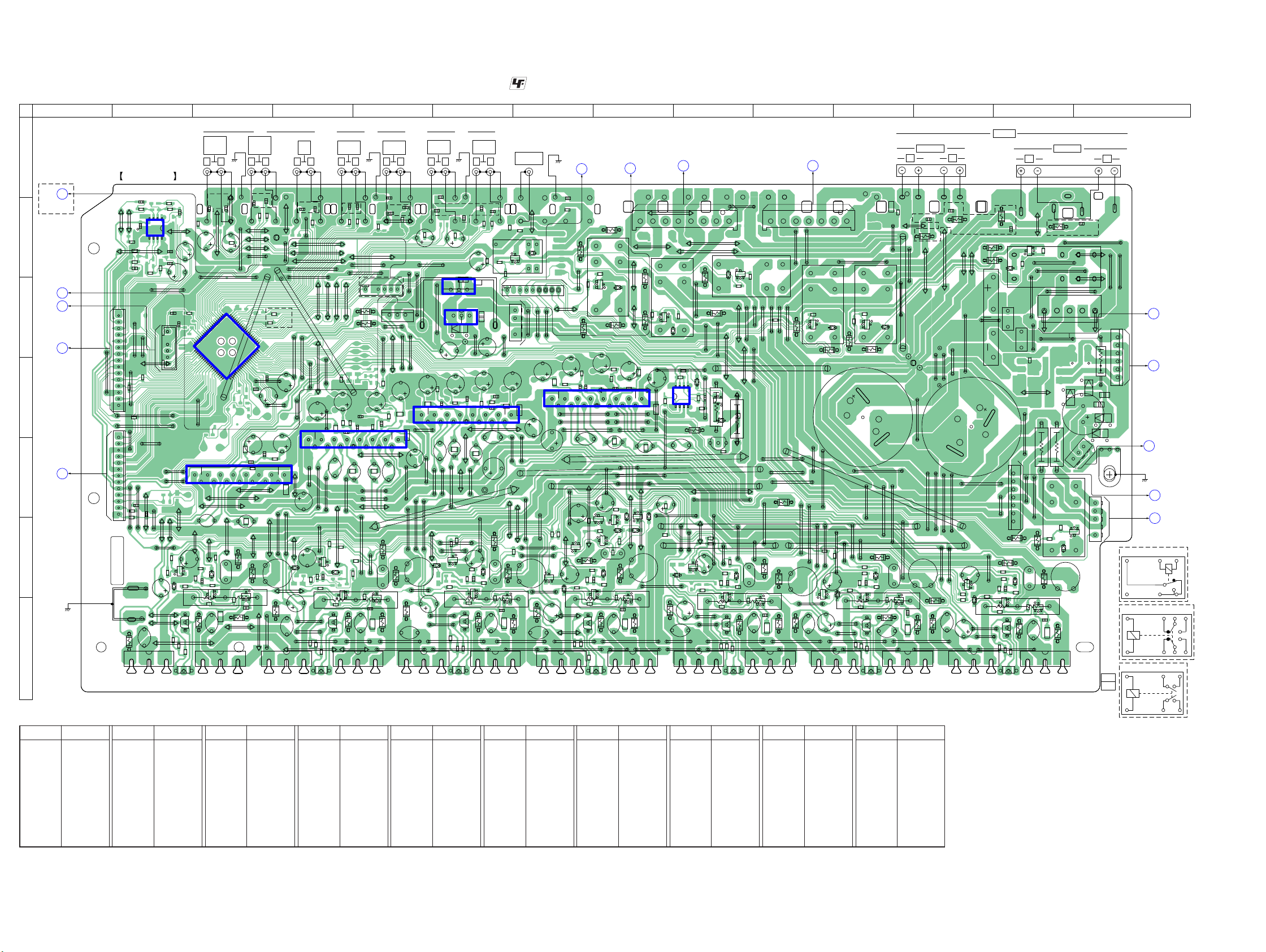
STR-DG820
STR-DG820
2020
B
E
B
E
B
E
BE
B
E
B
E
BE
B
E
BE
BE
B
E
B
E
B
E
20
21
41
60
40
61
80
1
B
E
B
E
B
E
B
E
B
E
B
E
BE
B
E
B
E
B
E
B
E
B
E
B
E
B
E
BE
B
E
B
E
B
E
B
E
B
E
B
E
B
E
D940
R401
D365
D941
R402
D942
R403
D943
R404
R405
R408
R409
D561
D370
Q661
R601
Q662
R602
R603
R604
R605
D375
R606
R607
R608
D761
D570
Q861
R801
Q862
R802
R803
Q670
R804
R611
R805
R806
R807
R614
R808
R615
R616
D770
Q870
R811
R620
R814
R621
R815
IC565
R622
R816
R623
R624
R431
R820
R821
R822
R823
JR398
R630
R824
C400
JR399
R632
C403
C405
R830
R449
C602
C604
R450
R451
R453
R454
R455
C802
R458
C804
R459
C611
R651
R652
R653
R654
R656
R657
R658
C811
R466
R467
C620
R851
R852
R853
C430
R854
C431
R661
R856
R857
R470
R664
R858
R665
R666
C820
R861
R670
R864
R671
R865
R866
R673
R674
R677
C449
R870
R871
R872
R873
C450
R680
R874
Q301
R880
C652
C654
Q501
C852
C854
C661
JR406
Q320
C861
Q321
Q323
C670
Q324
Q325
D611
IC400
Q711
Q712
C870
D811
C489
D620
Q720
D820
C499
JR434
Q920
JR435
JR632
Q350
Q355
Q360
R301
R304
Q365
Q561
R501
Q562
R502
R503
R504
Q370
R505
R506
R507
D661
Q375
Q761
R701
Q762
R702
R703
R704
Q570
R705
R706
R707
R320
R708
D861
R323
D670
R325
R326
R327
Q770
R328
R711
R714
R715
R716
D870
R720
R721
R722
R723
R724
CL001
R921
CL002
R923
CL003
R730
CL004
C500
CL005
CL006
CL007
CL008
R350
R353
R931
R355
C702
R358
C704
R551
R552
R553
R360
R554
R555
R556
R363
R557
R558
C711
R365
R368
R751
R752
R753
R754
R561
R756
R757
R758
R564
R370
R565
R566
R373
C720
R375
R378
R761
R764
R570
R765
R571
R766
R572
R573
R574
R770
R771
R772
R773
R774
C350
R580
C352
R780
C552
C554
CC01
D301
CC02
CC03
CC04
C940
CC05
C941
CC08
CC09
C752
C754
D500
C561
D501
CC11
CC12
CC13
CC14
C761
C570
D320
Q611
JR702
Q612
D325
D326
D327
C770
JR321
D711
JR322
Q811
C3022
Q812
Q620
C3025
C3026
C3027
D720
Q820
C3032
IC3002
C3037
R3010
D920
R3011
R3012
R3013
D350
CC51
CC52
D352
CC53
CC54
R3020
CC55
R3021
D355
R3022
R3023
CC58
CC59
D360
132
EB
132
I
O
132
1
5
1
8
1
7
E
B
1321
3
2
2
14
1
15
2
14
1
15
1
13
1
15
E
B
132132
E
B
132132
143
1
9
3
E
B
132132
E
B
132132
1
5
3
1
2
14
15
2
14
1
15
1
3
EB
132
4
IO
1
3
1
7
1
6
1
6
3
E
B
EBE
B
EB
EBEB
E
BEB
Q654
JW758
TB601
TB603
CNP912
JW760
Q851
JW761
Q852
JW762
Q853
Q854
HS350
IC350
IC352
JW766
JW767
JW768
JW769
CNP920
R609
JW770
JW771
JW772
JW773
R610
R612
JW776
R613
JW777
JS510
JS511
R809
JW779
R810
JW781
R812
CN602
JW782
R813
CN603
JW783
LP400
JS710
JS711
JW785
JS712
JW789
R628
CNP940
R629
L678
JW790
JS335
JW791
JS336
JS337
JS338
JW794
JS339
JW795
R828
JW798
R829
JW799
JS340
L878
C408
C409
JS920
JS921
C601
JS922
JS923
C603
JWH1
C605
JWH2
C606
JWH3
C607
CN434
JWH4
C608
JWH5
C609
JWH7
JS350
JWH9
C801
C803
JS930
C805
C806
C807
C808
C809
JS550
JS551
JS552
JS553
JS554
JS555
R659
JS556
JS557
JS558
JS559
C621
R660
R662
R663
JS560
JS3001
JS561
R859
C629
JS3002
JS562
JS563
JS564
JS565
C821
JS566
JS567
JS568
R860
JS569
R862
R863
C829
JS570
JS571
JS572
JS573
R678
R679
R487
R488
C644
R878
R879
JS3022
JS390
C458
JS391
C459
JS392
JS393
JS394
C844
JS395
C651
JS397
C653
JW600
JS399
C655
JW601
C656
JW602
C657
JW603
C658
JW604
Q500
C659
JW605
JW606
JW607
JW608
C851
JW609
JS3037
C853
JW800
C855
JW801
C856
JW802
C857
JW803
C858
JW610
JW804
C471
C859
Q701
JW611
Q702
JW612
Q703
JW613
JW807
Q704
JW614
JW615
JW616
JW617
JW618
JW619
C671
JW813
JW620
JW814
JW621
JW815
JW622
JW816
JW623
JW817
C679
JW819
JW626
C487
JW627
C488
C871
JW629
RR11
RR12
RR13
IC600
RR14
JW630
C879
JW631
JW825
JW632
JW826
JW633
JW827
JW634
JW635
JW829
JW636
JW637
IC800
JW638
JW639
JW830
JW831
JW832
JW833
JW640
JW834
JW641
JW835
JW642
JW836
JW643
JW837
JW644
CNP410
JW838
JW645
CNP411
JW839
JW646
JW647
JW648
L728
JW840
J401
JW841
JW842
J403
JW843
J404
JW650
J405
JW651
JW845
JW652
JW846
JW653
Q551
JW655
Q552
JW656
Q553
JW657
Q554
JW658
JW659
R302
R303
JW852
JW660
Q751
JW661
JW855
Q752
Q753
Q754
JW664
JW859
JW665
CNP432
JW667
JS400
JS401
JS402
JS403
JS404
JW860
JW861
JW862
JW863
JS408
JW864
JW670
JS409
JW671
JW866
JW672
JW867
JS600
JW868
R510
JS601
R511
JW675
JS602
JW676
JS603
JW677
JS410
JS604
JS411
JS605
R709
JW679
JS606
JS607
JS608
JWH10
JW870
JS609
JWH11
JW871
JWH12
JW872
R710
CN500
JW681
R712
R713
JS610
JW684
JS611
JW685
JS612
JW686
JW687
JW688
JW689
JS810
L578
JW690
JW691
JW692
JW693
JW694
JW695
JW696
R728
R729
JW699
JS432
L778
R920
GD1
GD2
R922
GD3
GD4
R545
R351
R546
R352
C701
R356
C703
R357
C705
C706
C707
C320
C708
C709
C323
R361
C325
R362
C904
R940
R559
R366
R367
JS458
JS459
R560
CN350
R562
R563
JS460
JS461
R759
R371
R372
C721
R376
R377
R760
R762
R763
C729
RY301
JS470
C920
CN941
JS471
C921
JS472
C922
JS473
C923
R578
R579
C544
C351
C545
C546
C353
R778
R779
R392 R393
C744
C551
C553
C555
C556
C557
C558
C559
C751
C753
JW700
C755
C756
C757
C758
JW704
C759
Q601
JW705
Q602
JW706
Q603
JW707
Q604
JW708
JW321
JW709
JW322
JW323
JW324
JW325
JW326
JW327
JW328
JW710
JW329
Q801
C571
Q802
JW712
Q803
JW713
Q804
JW714
JW715
JW716
JW717
JW330
JW718
RY920
JW331
C579
JW332
C771
CN792
IC500
JW720
JW721
C3024
RY350
C779
RY355
IC700
W001
ET902
W002
JW731
B400
RY360
C3034
CNP500
JW737
JW738
RY365
D921
JW739
L628
JW740
JW741
JW743
RY370
JW745
JW746
JW747
JW748
RY375
JW749
JSH550
L828
JSH551
JW750
JW751
JW752
JW753
JW754
Q651
JW755
Q652
JW756
Q653
1
8
4
5
1
6
1
8
4
5
(CHASSIS)
(CHASSIS)
1-875-588-
LR
FRONT B
FRONT A
RL
SPEAKERS
LR
TV
IN
LR
SA-CD/CD/
CD-R
IN
LR
SA-CD/CD/
CD-R
OUT
LR
SAT
AUDIO IN
LR
DVD
AUDIO IN
LR
VIDEO 1
AUDIO OUT
LR
VIDEO 1
AUDIO IN
SUB WOOFER
AUDIO OUT
(CHASSIS) (CHASSIS) (CHASSIS)
(CHASSIS)
J
MAIN POWER
TRANSFORMER
T901
MAIN POWER
TRANSFORMER
T901
L
STANDBY
BOARD
CN914
M
K
STANDBY BOARD
CN911
E
FRONT V2
BOARD
CN721
H
FRONT V2
BOARD
CN725
D
XM
BOARD
CN102
FRONT V2
BOARD
CN725
C
B
A
DIGITAL
AUDIO
BOARD
CN2222
DIGITAL
AUDIO
BOARD
CN2223
G
VIDEO
BOARD
CNP203
F
MICOM
BOARD
CN7005
N
SPFAKER
BOARD
CNP285
MAIN BOARD
(US, CND)
(US, CND)
(EXCEPT US, CND)
(EXCEPT US, CND)
(EXCEPT US, CND)
(EXCEPT US, CND)
(EXCEPT US, CND)
(EXCEPT US, CND)
(EXCEPT US, CND)
(EXCEPT US, CND)
(EXCEPT US, CND)
P
SPFAKER
BOARD
CNP286
A
B
C
D
E
F
G
12345678910111213 14
RY350, 355, 360, 365, 370, 375
-1
-2
RY301
RY920
-1
-2
12, 21
(12, 21)
6-6. PRINTED WIRING BOARD - MAIN Board -
• : Uses unleaded solder.
• See page 19 for Circuit Boards Location.
Ref. No. Location Ref. No. Location Ref. No. Location Ref. No. Location Ref. No. Location
Ref. No. Location
• Semiconductor Location
Ref. No. Location Ref. No. Location Ref. No. Location Ref. No. Location
D301 B-7
D320 F-8
D325 F-8
D326 E-8
D327 E-8
D350 C-11
D352 C-6
D355 B-9
D360 C-8
D365 C-10
D370 C-8
D375 F-13
D500 D-9
D501 D-9
D561 F-2
D570 F-3
D611 F-7
D620 F-8
D661 F-4
D670 F-4
D711 F-9
D720 F-9
D761 F-6
D770 F-6
D811 F-12
D820 F-13
D861 F-11
D870 F-11
D920 B-13
D921 C-12
D940 D-14
D941 D-14
D942 D-13
D943 D-14
IC350 C-6
IC352 C-6
IC400 C-3
IC500 E-3
IC565 D-9
IC600 E-4
IC700 D-6
IC800 D-7
IC3002 B-2
Q301 B-7
Q320 E-8
Q321 E-7
Q323 F-8
Q324 F-8
Q325 E-8
Q350 C-11
Q355 B-9
Q360 C-8
Q365 C-10
Q370 C-8
Q375 F-13
Q500 E-9
Q501 D-9
Q551 G-2
Q552 G-2
Q561 F-3
Q562 F-3
Q570 F-2
Q601 G-7
Q602 G-8
Q611 F-8
Q612 F-7
Q620 F-7
Q651 G-4
Q652 G-4
Q661 F-5
Q662 F-4
Q670 F-4
Q701 G-9
Q702 G-9
Q711 F-10
Q712 F-9
Q720 F-9
Q751 G-6
Q752 G-6
Q761 F-6
Q762 F-6
Q770 F-6
Q801 G-13
Q802 G-13
Q811 G-13
Q812 G-13
Q820 F-12
Q851 G-11
Q852 G-11
Q861 F-11
Q862 F-11
Q870 F-10
Q920 B-13
(Page 36)
(Page 40)
(Page 44)
(Page 44)
(Page 46)
(Page 46)
(Page 46)
(Page
46)
(Page
42)
(Page 28)
(Page 42)
(Page 42)
(Page 33)
(Page 33)
Ver. 1.1
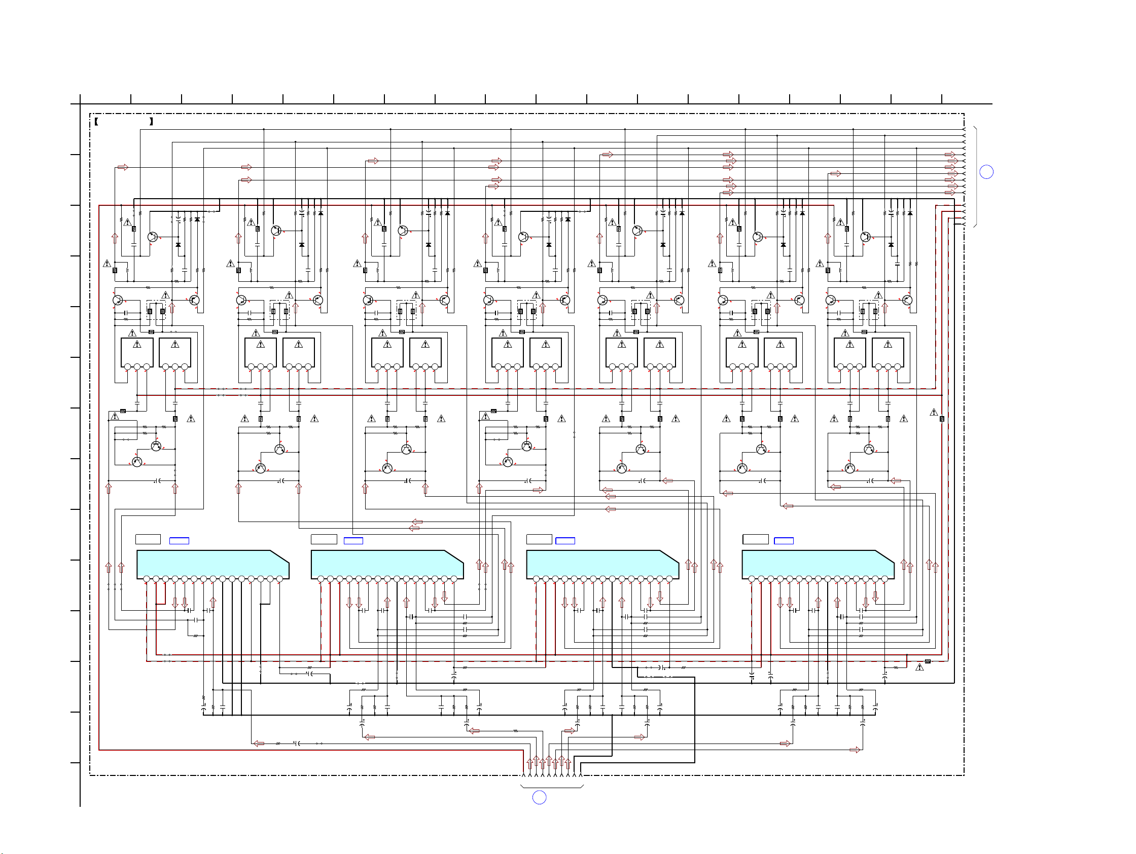
STR-DG820
STR-DG820
2121
• See page 48 for IC Block Diagrams.
6-7. SCHEMATIC DIAGRAM - MAIN Board (1/3) -
2
IC B/D
IC B/D
(2/3)
BOARD
MAIN
(3/3)
MAIN
BOARD
1
IC B/D IC B/D
0
1.1
-35.7
0
35.7
-1.1
0
-35.7
1.1
-1
0
35.7
0
-35.7
1.1
-1.1
0
35.7
0
-35.7
1.1
-1.1
0
35.7
0
-35.7
1.1
-1.1
0
35.7
0
-35.7
1.1
-1.1
0
35.7
0
-35.7
1.1
-1.1
0
35.7
0
0
0
0
0
0
0
0
0
0
0
0
0
0
0
0
0
0
0
0
0
-35
0
0
0
-35
0
0
-35
0
0
-35
0
0
-35
0
0
-35
0
0
-35
0
2.7
00
2.7
0
2.70
2.7
0
2.7
0
2.70
2.7
-1.11.1
0.5
-1.1
-0.6-0.6
-1
0.4
1.1 -1
-0.6
-1.1
0.5
1.1 -1.1
-0.6
-1.1
0.5
1.1 -1.1
-0.6
-1.1
0.5
1.1 -1.1
-0.6
-1.1
0.5
1.1 -1.1
-0.6
-1.1
0.5
1.1 -1.1
-35.4
35.7
1.1
-1
-34
0
0
0
0
-33.8
-1.1
1.1
2.3
35.7
0
-1.1
35.7
2.2
0
-33.8
-35.4
35.7
-33.9
0
-1.1
0
1.1
1.1
0
-1.1
35.7
2.3
0
-33.8
-35.4
35.7
-33.8
0
-1.1
0
1.1
1.1
0
35.7
2.2
0
-35.4
-35.4
35.7
-33.7
-1.1
1.1
19876543215 14 13 12 11 10
UPC2581V-S
IC500
MUTE
-VOUT1
+VOUT1
COMP1
NF1
IN1
GND
IN2
NF2
COMP2
-VOUT2
+VOUT2
VCC
VCC
VEE
R555 22k
2SA1163L-TE85L
Q562
2SA1163L-TE85L
Q561
L578
123
BCE
2SA1115TP-EF
Q551
5W0.22
R563
10
R579
1.5k
R564
15k
R572
15kR565
123
BCE
4.7
R578
50V10
C571
2.2k
R556
47k
R580
220p
C561
560
R558
68k
R566
6.2kR562
0.022
C579
4.7k
R561
82k
R557
25V
47
C557
500V
47p
C559
0.01C570
500V
C558
47p
2SC3623ATP-LK
Q552
2SA1163L-TE85L
Q611
560
R658
500V
47p
C609
15k
R672
500V
C658
47p
2SA1115TP-EF
Q601
123
BCE
6.2kR662
47k
R680
2.2k
R656
10 50V
C621
25V47
C607
2SA1163L-TE85L
Q662
1.5kR664
2SC3623ATP-LK
Q602
2SA1115TP-EF
Q651
82k
R607
L628
1.5k
R614
15k
R622
4.7k
R611
560
R608
50V10
C671
0.022
C679
82k
R657
220p
C611
4.7kR661
R628
4.7
0.022
C629
2SA1163L-TE85L
Q661
68kR666
123
BCE
25V
47
C657
123
BCE
10
R679
R629
10
15k
R615
123
BCE
47k
R630
L678
15kR665
R663
2SA1163L-TE85L
Q612
2.2k
R606
0.01C670
R613
0.01C620
6.2kR612
220pC661
68k
R616
2SC3623ATP-LK
Q652
500V
47p
C659
4.7
R678
2SA1163L-TE85L
Q711
560
R808
R813
123
MN2488-OPY-MK
Q803
BCE
47k
R830
R863
500V
C758
47p
2SA1163L-TE85L
Q862
2SA1115TP-EF
Q701
123
BCE
25V47
C807
4.7kR811
47k
R780
82k
R857
2SA1115TP-EF
Q801
68kR854
2SA1163L-TE85L
Q762
1.5kR764
2SC3623ATP-LK
Q702
4.7kR861
1.5kR714
100p
C804
500V
C708
47p
0.01C870
560
R708
50V10
C771
123
MP1620-OPY-MK
Q804
BCE
220pC711
4.7kR761
500V3p
C805
25V
47
C857
68kR766
68kR704
1.5kR814
R805
22k
25V
47
C757
123
BCE
10
R779
10
R729
19876543215 14 13 12 11 10
UPC2581V-S
IC800
MUTE
+VOUT1
-VOUT1
COMP1
NF1
IN1
GND
IN2
NF2
COMP2
-VOUT2
+VOUT2
VCC
VCC
VEE
L878
15kR815
500V3p
C855
123
BCE
15k
R822
2SA1163L-TE85L
Q712
2.2k
R706
500V
C858
47p
0.01C720
1.5kR864
R705 22k
100p
C704
220pC761
2SC3623ATP-LK
Q752
100p
C754
4.7
R778
560
R758
500V
47p
C709
0.01C820
15k
R772
2SA1163L-TE85L
Q811
68kR754
100p
C854
2.2k
R856
0.022
C879
500V
47p
C809
2SA1163L-TE85L
Q812
2.2k
R756
68kR804
50V10
C721
L828
123
BCE
220pC861
500V3p
C705
25V47
C707
68kR816
2SA1115TP-EF
Q851
2SA1115TP-EF
Q751
50V10
C821
10
R879
82k
R707
19876543215 14 13 12 11 10
UPC2581V-S
IC700
MUTE
+VOUT1
-VOUT1
COMP1
NF1
IN1
GND
IN2
NF2
COMP2
-VOUT2
+VOUT2
VCC
VCC
VEE
L728
2.2k
R806
15k
R722
4.7kR711
10
R829
500V
C808
47p
0.022
C779
2SA1163L-TE85L
Q861
82k
R757
560
R858
4.7
R728
0.022
C729
2SA1163L-TE85L
Q761
123
BCE
6.2kR862
500V
47p
C859
15kR865
15k
R872
68kR866
47k
R880
15kR715
L778
4.7
R878
6.2kR812
15kR765
2SC3623ATP-LK
Q852
R763
0.01C770
R713
6.2kR712
82k
R807
500V3p
C755
50V
10
C871
123
BCE
0.022
C829
68kR716
4.7
R828
220pC811
500V
47p
C759
100V
10
C546
1
R546
1
R545
100V
10
C545
500V3p
C605
500V3p
C655
19876543215 14 13 12 11 10
UPC2581V-S
IC600
MUTE
+VOUT1
-VOUT1
COMP1
NF1
IN1
GND
IN2
NF2
COMP2
-VOUT2
+VOUT2
VCC
VCC
VEE
1k
R601
50V
C601
10
68kR604
100p
C602
100p
C654
100p
C604
50V
C651
10
R605
22k
1k
R651
100p
C652
68kR654
68k
R652
1k
R751
1k
R701
50V
C751
10
100p
C752
100p
C702
50V
C701
10
68k
R752
68k
R702
1k
R851
1k
R801
50V
C851
10
100p
C852
100p
C802
50V
C801
10
68k
R852
68k
R802
R730
47k
MA2J1110GLS0
D661
MA2J1110GLS0
D570
MA2J1110GLS0D870
MA2J1110GLS0D820
MA2J1110GLS0
D611
MA2J1110GLS0
D861
MA2J1110GLS0
D561
MA2J1110GLS0D670
MA2J1110GLS0
D811
MA2J1110GLS0
D761
MA2J1110GLS0D770
MA2J1110GLS0D720
MA2J1110GLS0
D620
MA2J1110GLS0
D711
100p
C554
500V33p
C553
68k
R552
1k
R551
500V
3p
C555
100p
C552
R554
68k
50V
C551
10
JR632 0
22kR720
22kR670
22kR870
22kR770
22kR820
22kR620
22kR570
50V
C644
10
50V
C844
10
50V
C744
10
50V
C544
10
500V33pC603
4.7k
R771
4.7k
R821
4.7k
R871
4.7k
R621
22k
R824
22k
R674
22k
R724
22k
R624
22k
R874
22k
R574
22k
R774
47k
R573
47k
R773
47kR873
47kR723
47k
R673
47kR823
47k
R623
100
R760
100
R859
100
R709
100
R809
100
R810
100
R860
100
R710
100
R660
100
R659
100
R759
100
R560
100
R559
100
R610
100
R609
2.2kR853
2.2kR703
2.2kR803
2.2kR753
R553
2.2k
2.2kR653 2.2kR603
JS712
JS710
JS610
JS611
JS511
JS810
JS711
500V
C608
47p
6.2kR762
JS556
JS557
JS558
JS559
JS560
JS561
JS562
JS563
JS564
JS565
JS566
JS567
JS568
JS569
JS570
JS571
JS572
JS573
JS604
JS605
JS606
JS607
JS608
JS609
JS612
68k
R602
500V
33p
C853
500V
33p
C803
500V
33p
C653
500V
33p
C703
500V
33p
C753
10V
C706
220
10V
C606
220
10V
C756
220
10V
C556
220
10V
C856
220
10V
C656
220
10V
C806
220
4.7k
R671
4.7k
R721
4.7k
R571
70
71
72
73
74
75
76
77
78
79
80
81
82
83
84
868788899192939495
96
POWER AMP
IC600
POWER AMP
IC700
(1/3)
MAIN BOARD
BOOSTER BOOSTER
BIAS
Q801, 802
BIAS
Q851, 852
BIAS
Q701, 702
BIAS
Q601, 602
BIAS
Q751, 752
BIAS
Q651, 652BIAS
Q551, 552
711
D
B
1669 1710
F
5
N
15
L
K
3
G
1 1812
C
M
E
H
8
J
4 13
A
142
I
2SC3052EF-T1-LEF
Q570
AF POWER
SENSOR
DETECT
CURRENT
Q561, 562
MP1620-OPY-MK
Q554
BOOSTER
MN2488-OPY-MK
Q553
BOOSTER
POWER AMP
IC500
POWER AMP
IC800
MP1620-OPY-MK
Q654
BOOSTER
MN2488-OPY-MK
Q653
BOOSTER
MN2488-OPY-MK
Q753
BOOSTER
MP1620-OPY-MK
Q754
BOOSTER
MN2488-OPY-MK
Q603
BOOSTER
MP1620-OPY-MK
Q604
BOOSTER
MN2488-OPY-MK
Q703
BOOSTER
MP1620-OPY-MK
Q704
BOOSTER
MN2488-OPY-MK
Q853
BOOSTER
MP1620-OPY-MK
Q854
BOOSTER
2SC3623ATP-LK
Q802
2SC3052EF-T1-LEF
Q820
Q811, 812
CURRENT
DETECT
AF POWER
SENSOR
2SC3052EF-T1-LEF
Q870
AF POWER
SENSOR
DETECT
CURRENT
Q861, 862
2SC3052EF-T1-LEF
Q720
AF POWER
SENSOR
DETECT
CURRENT
Q711, 712
2SC3052EF-T1-LEF
Q620
AF POWER
SENSOR
DETECT
CURRENT
Q611, 612
2SC3052EF-T1-LEF
Q770
AF POWER
SENSOR
DETECT
CURRENT
Q761, 762
2SC3052EF-T1-LEF
Q670
AF POWER
SENSOR
DETECT
CURRENT
Q661, 662
5W0.22
5W0.22
5W0.22
5W0.22
5W0.22
5W0.22
(Page 23)
(Page 22)
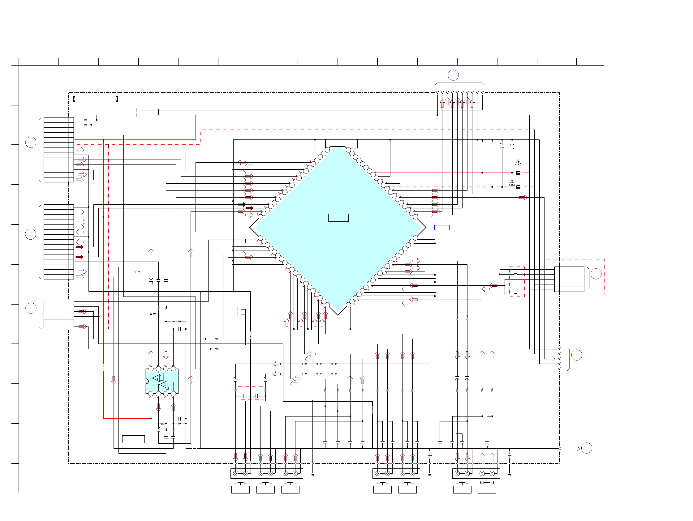
STR-DG820
STR-DG820
2222
• See page 48 for IC Block Diagrams.
6-8. SCHEMATIC DIAGRAM - MAIN Board (2/3) -
IC B/D
BOARD
XM
D
CN102
3
BOARD
MAIN
(3/3)
BOARD
(3/3)
4
MAIN
V2
FRONT
C
CN725
BOARD
CN2223
BOARD
(2/2)
B
DIGITAL
AUDIO
DIGITAL
A
(2/2)
BOARD
AUDIO
CN2222
2
(1/3)
MAIN
BOARD
0
0
0
0
0
0
0
0
0
-6.8
0.6
0.6
6.9
0.1
0.2
0.2
0.2
0
0
0
0
0
0
0
0
0
0
0
0
0
0
0
0
0
0
0
0
0
0.2
0.2
0
0
0
0
0
0
07
0
0
0
0
0
-6.9
R3011
47k
C3037
1
C3032 1
R3022
47k
C3025
0.1
C3022
1
R3020
47k
C3026
0.1
8765
4321
NJM4565M(TE2)
IC3002
CC02
100p
CC52
100p
50V
C409
4.7
R451
1k
50V
C459
4.7
R402
1k
R459
1k
R409
1k
CC01
100p
CC51
100p
CC09
100p
R401
1k
R452
1k
J401
6P
CC59
100p
R453
1k
CC03
100p
CC53
100p
R403
1k
R454
1k
CC04
100p
CC54
100p
R404
1k
C403
2200p
R405
1k
50V
C458
4.7
R455
1k
R408
1k
CC05 100p
CC08 100p
50V
C408
4.7
CC58 100p
CC55 100p
R458
1k
C405
2200p
0.1
C489
100pC449
0.1
C499
100pC450
JR434
0
JR435
0
C430 220p
C431
220p
1
2
3
4
5
6
7
8
9
10
11
12
13
14
15
16
17
18
19
20
21
22
23
24
25
26
27
28
29
30
31
32
33
34
35
36
37
38
39
40
41
42
43
44
45
46
47
48
49
50
51
52
53
54
55
56
57
58
59
60
61
62
63
64
65
66
67
68
69
70
71
72
73
74
75
76
77
78
79
80
GND
GND
RECL4
RECR4
RECL3
RECR3
RECL2
RECR2
RECL1
RECR1
GND
INL16
INR16
INL15
INR15
INL14
INR14
INL13
INR13
GND
INL12
INR12
INL11
INR11
INL10
INR10
INL9
INR9
INL8
INR8
INL7
INR7
INL6
INR6
INL5
INR5
INL4
INR4
INL3
(DCAC_MIC)
INR3
(DCAC_MIC)
INL2
DMPORT_L)
INR2
(DMPORT_R)
INL1 (TUNER_L)
INR1 (TUNER_R)
GND
SBLIN
SBRIN
SLIN
SRIN
CIN
SWIN
LIN
RIN
GND
ROUT
LOUT
GND
ROUT SUB
LOUT SUB
GND
13P
CNP410
15P
CNP411
R3023
47k
R430
1k
R431 1k
JS409 JS410 JS411
JS461JS459 JS460
JS400
1kR449
1k
R450
JS408
JS458
JS3002
JS3037
JS3022
JS3001
J403
4P
J404
4P
JS401
1
3
4
5
6
6P
CN434
XMR
XMGND
XML
-7V
+7V
R488
2.2
25V
C488
47
94
88
89
91
87
96
86
93
92
95
97
98
99
100
101
W001-002
MAIN BOARD (2/3)
VEE
VCC
6P
CNP432
(CHASSIS)
(CHASSIS) (CHASSIS)
(EXCEPT US,CND)
(EXCEPT US,CND)
(US,CND)
SA-CD/CD/
R
TV IN
RLRLL
SA-CD/CD/
CD-R INCD-R OUT
DVD AUDIO
RRLL
IN IN
SAT AUDIO
L
AUDIO OUT AUDIO IN
VIDEO 1 VIDEO 1
RRL
(EXCEPT US,CND)
711
D
B
6910
F
5 15
K
3
G
1 12
C
E
H
8
J
4 13
A
142
I
MIX AMP
IC3002
BD3471KS2
IC400
IC400
INPUT SELECTOR,
ELECTRICAL VOLUME
GND
HPFN
LPF01
LPF02
LPFN2
LPFN1
SWVOL
VCC
DGND
DATA
CLK
VEE
FROUT
FLOUT
SWOUT
COUT
SROUT
SLOUT
SBROUT
SBLOUT
VIDEO2-AU_R
NC
MIC_GND
A-GND
MIC MONO
VIDEO2-AU_L
2
6
4
3
5
1
AGND
SL OUT
+7V
SBR OUT
SBL OUT
L IN
AGND
R IN
TUNER R
AGND
TUNER L
DMPORT L-
DMPORT R-
DMPORT L+
DMPORT R+
1
2
3
4
5
6
7
8
9
10
11
12
13
14
15
VOL IC CLK
VOL IC DATA
VACS CTRL
PROTECTOR
+7V
-7V
FR OUT
AGND
FL OUT
SW
AGND
C OUT
SR OUT
1
2
3
4
5
6
7
8
9
10
11
12
13
50V
C3034
4.7
R3021
47k
C3027
1
R3012
47k
R3013
47k
R3010
47k
50V
C3024
4.7
R487
2.2
25V
C487
47
(Page 21)
(Page
35)
(Page
35)
(Page
43)
(Page 29)
(Page 23)
(Page 23)
Ver. 1.1
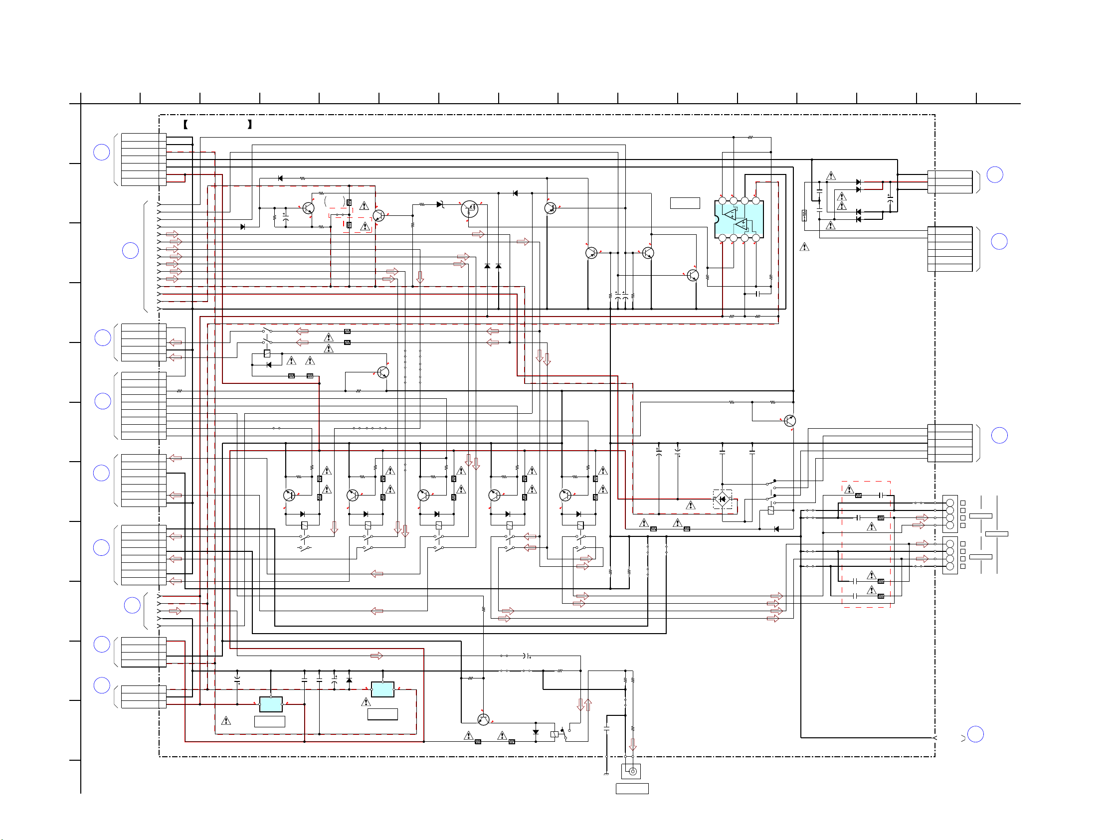
STR-DG820
STR-DG820
2323
6-9. SCHEMATIC DIAGRAM - MAIN Board (3/3) -
MAIN
4
(2/3)
BOARD
CN911
K
STANDBY
BOARD
1
BOARD
MAIN
(1/3)
BOARD
CN721
E
FRONT
V2
CN7005
F
MICOM
BOARD
CN285
N
SPEAKER
BOARD
SPEAKER
P
CN286
BOARD
(2/3)
BOARD
3
MAIN
CNP203
G
VIDEO
BOARD
BOARD
CN725
H
FRONT
V2
MAIN POWER
M
T901
TRANSFORMER
TRANSFORMER
T901
J
MAIN POWER
CN914
BOARD
STANDBY
L
-5.5
0.7
-6.9
7
-5.5
-4.4
-5.5
0
3.8
3.8
0
-35.1
0
0
6.3 6.4
-5.5
-35.6
-35.1
-35.9
-35.7
3.6
-35.7
16
0.5
-35.1
16
0.6
-17.1
16
-6.9
7
0.7
0
0.70.70.70.70.7
0.10.10.10.10.1
C400
2200p
RY301
50VC471 4.7
R467
100k
RY920
2.2k
R921
1
2
3
4
5
5P
CNP920
R1 (UPPER TAP)
R1 (LOWER TAP)
R1 GND
R1 (LOWER TAP)
R1 (UPPER TAP)
39k
R326
2SC3052EF-T1-LEF
Q324
50V10C325
2SA1163L-TE85L
Q323
10k
R327
6.8kR325
2SC2713G-TE85L
Q325
2SA1163L-TE85L
Q320
2SC3052EF-T1-LEF
Q321
1k
R328
10k
R503
220k
R507
10k
R504
8765
4321
470k
R502
10kR505
0.1
C500
1SR154-400TE-25D352
0.47
C350
0.47
C352
1SR154-400TE-25D943
0.47C940
0.47
C941
1SR154-400TE-25D940
2.2kR375
RY375
RY365
2SC3052EF-T1-LEF
Q365
2.2k
R365
2SC3052EF-T1-LEF
Q360
RY360
2SC3052EF-T1-LEF
Q355
RY355 RY350
2SC3052EF-T1-LEF
Q350
2.2k
R350
RT1P241C-TP-1
Q501
1k
R355
1k
R360
R301
2.2k
MA2J1110GLS0
D360
MA2J1110GLS0
D365
MA2J1110GLS0
D920
MA2J1110GLS0
D326
MA2J1110GLS0
D501
MA2J1110GLS0
D350
MA2J1110GLS0
D325
MA2J1110GLS0
D355
MA2J1110GLS0
D375
MA2J1110GLS0
D320
MA2J1110GLS0D327
MA2J1110GLS0
D301
RY370
MA2J1110GLS0
D370
2SC3052EF-T1-LEF
Q370
R370
2.2k
1
2
3
4
5
6
6P
CNP940
F1
NC
GND
F2
R4 -AC
R4 +AC
10
RR12
3P
CNP500
R371
33
R372
47
47
R367
33
R366
47
R362
33
R361
47
R357
33
R356
47
R352
33
R351
47
R37733R376
R302
100
R303
100
47
R922
JS390
33
R920
D5SBA20-4003
D921
~
~
C923 0.01F 71V
C922
0.01F
71V
2W
680
R393
2W
R392
680
JS510
2W
R510
100
MAZ8300GMLS0
D500
10k
R501
JS397
47kR506
1
2
3
4
5
6
7
8
8P
CN602
1
2
3
4
5
6
7
7P
CN603
JSH550
JS550
JS551
JS552
JS553
JS554
JS555
JS600
JS601
JS602
JS603
JS470 JS471
JS472
JS473
JS350
JS395
JS393
JS394
JS392
JS391
JR406 0
∗
R511
JSH551
IO
G
TA7807S
IC350
12
3
12
3
47k
R373
47k
R358
47k
R363
47k
R368
47k
R353
47k
R304
47k
R378
47k
R923
J405
1
2
3
4
5
6
7
7P
CNP912
1
2
3
3P
CN941
GND (R4)
+7V (R4)
GND (R4)
10V330C320
10V330
C323
20k
R320
39k
R323
1/2W
0.15
R940
16V
100
C353
81
78
84
83
80
76
77
82
74
73
70
72
79
71
75
101
98
99
100
97
0
JR3980JR399
W001-002
MAIN BOARD (3/3)
VCC
VEE
AF POWER PROTECTOR
Q320, 321, 323-325
RELAY DRIVE
RELAY DRIVE
RELAY DRIVE
RELAY DRIVE
RELAY DRIVE
LIMITTER SWITCH
Q500, 501
-2
-1
-1
-2
-1
-2
-1
-2
-1
-2
-1
-2
(CHASSIS)
-1
-2
470 2W (EXCEPT US,CND)
∗R511
330 2W (US,CND)
EXCEPT
US,CND
(US,CND)
(EXCEPT US,CND)
CN500
4P
3
3
4
2
2
1
1
CN792
5
5P
3
4
2
1
CN350
5
9P
3
4
2
1
6
7
8
9
R
L
R
L
L
R
R
L
711
D
B
166910
F
5 15
L
K
3
G
1 12
C
E
H
8
J
4 13
A
142
I
R2 RETURN GND
HP_GND
-15V
STBY GND
R2 GND
+15V
+15V
NC
HP DETECT
R-CH
L-CH
GND
SW_PREOUT_RY
NC
HP_DET
HP_RY
FRONT_A/B
C/SR/SBL RY
FRONT_A_RY
SBR_RY
BRIDGEABLE RY
SR
SR_GND
NC
SBL
SBL_GND
NC
SBR
SBR_GND
C
NC
C_GND
NC
NC
SL
SL_GND
+7V
GND
-7V
NC
+15V
GND
-15V
2SC1815GR-TPE2
Q500
NJM4565M(TE2)
IC565
OVER LOAD DETECTOR
IC565
FRONT A
TB601
TB603
FRONT B
+
+
-
-
+
+
-
-
IC352
-7V REGULATOR
IC350
+7V REGULATOR
TA79007SB
IC352
IO
G
16V
100
C351
2SC3052EF-T1-LEF
Q375
RELAY DRIVE
16V
3300
C904
1SR154-400TE-25
D941
1SR154-400TE-25
D942
10
RR13
10
RR14
10
RR11
0.01
CC12
0.01
CC13
0.01
CC14
0.01
CC11
R466
1k
R470
47k
2SC3052EF-T1-LEF
Q301
RELAY DRIVE
AUDIO OUT
SUB WOOFER
100V
0.22
C921
2SC3052EF-T1-LEF
Q920
RELAY DRIVE
100V
0.22
C920
SPEAKERS
(Page
47)
(Page 21)
(Page 43)
(Page 37)
(Page 44)
(Page 44)
(Page
22)
(Page 41)
(Page 43)
(Page 47)
(Page 47)
(Page 47)
(Page 22)
Ver. 1.1
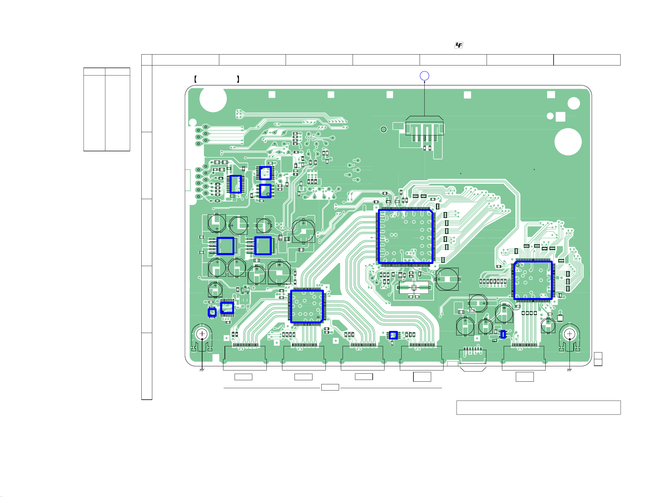
STR-DG820
STR-DG820
2424
1
5
1
19
1
19
1
19
1
19
1
19
R3610
R3611
R3612
R3613
L3506
ET3501
ET3502
R3645
R3649
R3651
R3654
R3655
JL3506
JL3507
JL3508
JL3509
CN3500 CN3501 CN3502 CN3503 CN3505
CN3507
Q3505
JL3543
JL3544
C3511
JL3545
JL3546
JL3547
JL3548
JL3549
C3518
JL3550
IC3501
IC3502
C3533
IC3503
IC3504
C3534
IC3505
IC3506
IC3507
C3538
IC3508
R3510
R3511
R3514
R3515
R3517
IC3510
R3518
IC3511
IC3512
C3543
IC3513
C3544
C3545
C3546
C3547
R3520
TP3000
R3521
R3523
R3524
R3529
C3554
R3530
R3532
R3533
C3562
R3541
R3548
C3571
C3576
C3577
C3579
R3554
C3580
C3584
C3586
C3587
CL3000
R3561
C3589
CL3001
CL3002
R3563
CL3003
CL3004
R3565
CL3005
CL3006
R3567
CL3007
FL3500
C3590
R3568
CL3008
FL3501
C3591
CL3009
FL3502
FL3503
C3593
R3570
CL3010CL3011
R3572
CL3012
R3573
CL3013
CL3014
R3575
CL3015
CL3016
R3577
CL3017
R3578
CL3018
CL3019
R3580
CL3020
CL3021
R3582
CL3022
R3583
CL3023
CL3024
R3585
CL3025
R3586
CL3026
R3587
CL3027
R3588
CL3028
R3590
R3593
R3594
R3595
R3596
R3597
R3598
R3599
RB3500
RB3501
RB3502
RB3503
RB3504
RB3505
RB3506
RB3507
RB3508
RB3509
CN3001
RB3510
RB3511
RB3512
RB3513
RB3514
RB3515
RB3516
RB3517
C3000
C3001
C3002
C3003
C3004
C3005
C3006
X3500
C3602
C3603
C3604
C3605
R3002
C3606
R3004
R3005
C3609
R3006
R3008
R3009
C3610
R3010
R3011
R3012
R3013
R3014
R3016
FB3500
FB3503
FB3504
FB3505
FB3506
FB3507
R3020
FB3509
R3023
R3600
R3602
R3603
FB3510
R3029
R3606
R3607
R3608
R3609
T
DCDC BOARD
CN4101
(CHASSIS)(CHASSIS)
18
4
5
1
1
10
11
20
8
16
9
1
8
4
5
1
20
60
41
40 21
1
25
75
51
100 76
26
5
43
1
50
61
80
1
10
11
E
20
1
8
45
1
36
108
73
109
144
72
37
1
5
1
5
1-875-647-
12
(12)
HDMI BOARD (COMPONENT SIDE)
A
B
C
D
E
1234567
HDMI
BD IN
(NC)
DVD IN
SAT IN
VIDEO 1
IN
HDMI
OUT
6-10. PRINTED WIRING BOARD - HDMI Board (Component Side) -
• : Uses unleaded solder.
• See page 19 for Circuit Boards Location.
Ref. No. Location
• Semiconductor
Location
IC3501 D-3
IC3502 E-4
IC3503 D-2
IC3504 B-2
IC3505 B-2
IC3506 C-4
IC3507 B-2
IC3508 D-6
IC3510 E-10
IC3511 C-2
IC3512 C-2
IC3513 D-1
Q3505 D-2
Note: When IC3506 and IC3508 cannot exchange with single. When IC3506
and IC3508 are damaged, exchange the entire mounted board.
(Page 45)
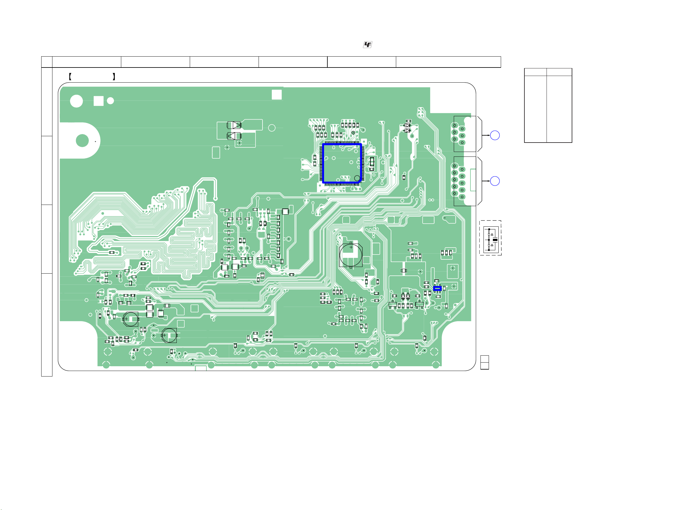
STR-DG820
STR-DG820
2525
6-11. PRINTED WIRING BOARD - HDMI Board (Conductor Side) -
• : Uses unleaded solder.
• See page 19 for Circuit Boards Location.
R3030
R3031
R3032
R3033
R3034
R3035
R3036
R3037
R3038
L3500
L3501
L3502
L3503
L3504
L3505
R3621
R3622
R3623
R3624
R3625
R3626
R3627
R3628
R3629
C3651
R3630
R3631
R3632
R3633
R3634
R3635
R3636
R3637
R3638
R3639
R3640
R3641
R3644
R3646
R3647
R3648
R3650
R3652
R3653
JL3500
JL3501
JL3502
JL3503
JL3504
JL3505
JL3510
JL3511
JL3512
X3000
JL3523
JL3524
JL3525
JL3526
JL3527
JL3528
JL3529
JL3530
JL3531
JL3532
JL3533
JL3534
JL3535
JL3536
C3503
JL3537
FB3000
Q3500
JL3538
C3505
Q3501
JL3539
C3506
C3507
C3508
C3509
JL3540
JL3541
JL3542
C3510
C3512
C3513
C3514
C3515
C3516
C3517
C3519
JL3551
JL3552
C3520
C3521
C3522
C3523
C3524
D3500
D3501
C3525
C3526
C3527
C3528
R3501
C3529
R3503
R3505
C3530
R3508
R3509
C3531
C3532
C3535
D3511
D3512
C3539
IC3509
R3512
C3540
C3541
C3542
C3548
C3549
R3522
R3525
R3526
R3527
C3550
R3528
C3551
C3552
C3553
C3555
C3556
C3557
C3558
C3559
R3531
R3536
C3560
C3561
C3563
C3564
C3565
C3566
C3567
C3568
C3569
R3542
R3543
R3545
R3546
R3547
C3570
C3572
C3573
C3578
R3551
R3552
R3553
R3556
R3557
R3558
R3559
C3581
C3582
C3583
C3585
R3560
C3588
R3562
R3564
R3566
C3592
C3598
R3571
C3599
R3574
R3579
R3589
R3591
R3592
C3600
D3000
D3001
R3001
R3003
C3608
IC3000
R3015
R3018
FB3508
R3021
R3024
R3025
R3026
R3027
R3604
R3028
R3605
1
25
75
76
100
50
26
51
1
2
9
10
1
2
5
6
CN3504
CN3003
1-875-647-
12
(12)
HDMI BOARD (CONDUCTOR SIDE)
A
B
C
D
12345 6
EE
13
4
5
S
R
MICOM BOARD
CN7002
MICOM BOARD
CN7003
X3000
Ref. No. Location
• Semiconductor
Location
D3000 A-6
D3001 A-6
D3500 D-6
D3501 D-6
D3511 A-3
D3512 A-3
IC3000 B-5
IC3509 D-6
Q3500 D-6
Q3501 D-5
(Page 36)
(Page 36)
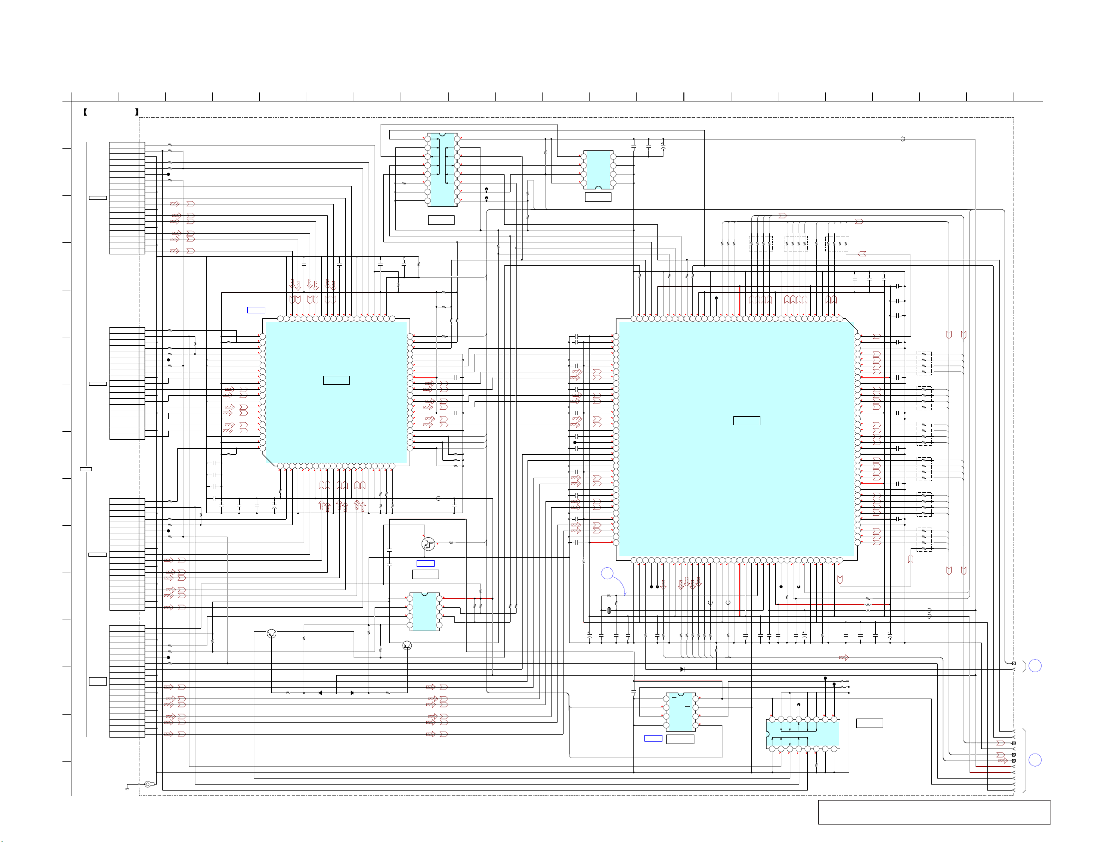
STR-DG820
STR-DG820
2626
1
HDMI
11
(2/2)
BOARD
12
HDMI
BOARD
(2/2)
IC B/D
IC B/D
IC B/D
1.8
3.3
3.3
3.3
3.3
3.3
3.3
3.3
3.3
3.3
3.3
3.3
3.3
1.8
0
3.3
3.3
3.3
3.3
3.3
3.3
3.3
3.3
3.3
3.3
3.3
3.3
1.8
0
0.4
0.4
3.303.3
000
0
1.2
1.2
1.2
3.3
1.2
1.2
1.2
1.2
3.3
1.8
1.2
1.2
1.2
1.2
1.8
1.8
1.4
1.9
3.3
1.2
1.2
1.2
1.2
1.2
3.3
1.8
1.2
1.2
2.1
2.1
1.8
2.1
2.1
2.1
2.1
3.3
2.1
2.1
2.1
2.1
1.8
2.1
2.1
2.1
2.1
3.3
2.1
2.1
2.1
0
00000
0
3.3
0
1.8
1.8
1.8
3.3
3.3
1.6
1.6
3.3
3.3
3.3
3.3
3.3
0
1.8
2.1
3.3
3.3
3.3
3.3
3.3
3.3
3.3
3.3
3.3
3.3
3.3
0
0
0
0
3.3
0
0
000
1.2
3.3
3.3
3.3
3.3
3.3
3.3
3.3
3.3
3.3
3.3
3.3
3.3
3.3
3.3
3.3
3.3
3.3
3.3
3.3
3.3
3.3
3.2
0
0
0
0.3
0.3
000
3.3
0
3.3
3.3
3.3
3.3
3.3
3.3
3.3
3.3
3.3
3.3
1.4
0.4
3.3
0.4
0
3.3
0.4
0.4
1.9
3.3
3.9
0
3.3
0.4
0.4
3.3
0
0
0
0
4.9
00000
4.9
0
4.9
4.9
0
3.3
3.3
3.3
3.3
0
4.9
10uH
L3500
0.1
C3556
0.1
C3539
0.1
C3538
0.1
C3528
0.1
C3524
0.1
C3525
0.1
C3526
0.1
C3527
0.1
C3529
0.1
C3521
0.1
C3522
0.1
C3530
0.1
C3523
0.1
C3532
0.1
C3535
0.1
C3541
10uHL3501
10uHL3502
0.1
C3545
0.1
C3549
6.3V
220
C3554
6.3V
220
C3555
47R3567
47
R3570
47
R3572
47
R3575
47
R3577
47
R3578
0.1
C3542
R3589 100
47
R3571
47
R3574
JL3500
JL3501
JL3502
0
R3501
0
R3503
0
R3505
0R3565
8
7
6
5
4
3
2
1
BR24L02F-WSE2
IC3505
10k
R3586
JL3508
JL3509
47k
R3522
47k
R3523
47k
R3524
22
RB3501
22
RB3502
47
RB3500
0
R3564
28.322MHz
X3500
1M
R3587
12p
C3544
15p
C3543
47
R3514
47
R3515
47
R3517
47
R3518
47
R3520
47
R3521
0.1
C3517
6.3V
220
C3518
JL3503
R3511 47
R3530
47k
R3510 47
R3508 0
0.1
C3548
47
R3566
0.1
C3552
0.1
C3553
R3568
0
0.1
C3550
R3591
4.7k
47
R3562
47
R3563
JL3505
JL3506
JL3507
JL3511
JL3512
JL3510
FB3503
6.3V
220
C3546
12345678910111213141516171819202122
2324252627282930313233343536
73 74 75 76 77 78 79 80 81 82 83 84 85 86 87 88 89 90 91 92 93 94 95 96 97 98 99
100
101 102 103 104 105 106 107 108
111
Q10
Q9
Q8
IOGND
ODCK
IOVCC33
Q7
Q6
Q5
Q4
CGND
CVCC18
Q3
Q2
Q1
Q0
IOGND
IOVCC33
DE
HSYNC
VSYNC
EVNODD
CGND
CVCC18
CVCC18
CSDA
CSCL
DSDA1
DSCL1
R1PWR5V
IOGND
IOVCC33
DSDA0
DSCL0
R0PWR5V
AGND
AVCC1 8
AVCC3 3
R0XC-
R0XC+
AGND
AVCC3 3
R0X0-
R0X0+
AGND
AVCC3 3
R0X1-
R0X1+
AGND
AVC33
R0X2-
R0X2+
AGND
AVCC1 8
RSVDNC
AVCC3 3
R1XC-
R1XC+
AGND
AVCC3 3
R1X0-
R1X0+
AGND
AVCC3 3
R1X1-
R1X1+
AGND
AVCC3 3
R1X2-
R1X2+
AGND
AVCC1 8
IOGND
IOVCC33
MUTEOUT
RSVDNC
RSVDNC
SPDIF
CGND
CVCC18
SD0
SD1
SD2
SD3WSSCK
IOGND
IOVCC33
MCLK
CGND
CVCC18
DVCC18
DGND2
XTALOUT
XTALIN
XTALVCC
REGVCC
RSVDNC
RSVDL
RESET#
SCDT
INT
IOGND
IOVCC33
CI2CA
CGND
CVCC18
Q35
Q34
Q33
Q32
IOGND
IOVCC33
Q31
Q30
Q29
Q28
CGND
CVCC18
Q27
Q26
Q25
Q24
IOGND
IOVCC33
Q23
Q22
Q21
Q20
CGND
CVCC
Q19
Q18
Q17
Q16
IOGND
IOVCC33
Q15
Q14
Q13
Q12
CGND
CVCC18
Q11
0.1
C3531
E
ET3501
12345678910
11 12 13 14 15 16 17 18 19
20
4142434445464748495051525354555657585960
RXTM
SDA_C
SCL_C
GND
CCLKN
CCLKP
VCC
CDT0N
CDT0P
GND
CDT1N
CDT1P
VCC
CDT2N
CDT2P
GND
VCC
REXT
OPACTRLN
CEC_TX
CVCC
HPD_B
SDA_B
SCL_B
GND
GND
BCLKN
BCLKP
VCC
BDT0N
BDT0P
GND
BDT1N
BDT1P
VCC
BDT2N
BDT2P
GND
VCC
HDP_C
4.7k
R3552
0
R3551
10k
R3553
10k
R3536
10k
R3554
47
R3557
10kR3558
10kR3559
10kR3560
1k
R3532
1k
R3531
1k
R3547
VCCA
SCLA
SDAA
GND EN
SDAB
SCLB
VCCB
R3545 47
R3546 47
C3511
0.1
C3508
0.1
JL3532
R3647 10k
0.1
C3514
R3648 10k
16 15 14 13 12
11 10 9
87654321
SN74LV4052APWR
IC3503
JL3504
0
R3541
JL3531
4.7k
R3652
1k
R3645
1k
R3644
R3542
4.7k
R3543
4.7k
1SS367-T3SONYD3000
DTC114YKA-T146
Q3505
0R3548
0
R3529
0
R3533
R3561
47
R3527
10k
ISA1235AC1TP-1EF
Q3501
R3525 4.7k
MA2J1110GLS0D3501
R3528
22k
4.7kR3512
10k
R3526
22k
R3509
MA2J1110GLS0D3500
G1
A1
Y2
GND A2
Y1
G2
VCC
0.1
C3610
0R3573
10k
R3649
10k
R3015
0.1
C3562
R3650
R3651
220
R3579
220
R3583
0.1
C3510
0.1
C3513
0.1
C3515
0.1
C3520
0.1
C3519
0.1
C3516
0.1
C3512
0.1
C3509
0.1
C3503
0.1
C3505
0.1
C3506
0.1
C3507
47
R3580
1k
R3588
1k
R3653
FB3500
FB3504
FB3505
68
R3582
68
R3585
22R3590
19P
CN3500
19P
CN3501
52
53
54
56
59
60
61
62
63
51
55
57
58
SCK
SPDIF
SD0
WS
MCK
SD2
SD3
SD1
Q[5]
Q[6]
Q[7]
Q[8]
Q[9]
Q[10]
Q[11]
Q[19]
Q[18]
Q[17]
Q[16]
Q[20]
Q[21]
Q[22]
Q[23]
ODCK
VSYNC
HSYNC
DE
1444_HPD
RX_INT
RX_RST
Q[24]
Q[25]
Q[26]
Q[27]
Q[0]
Q[1]
Q[2]
Q[3]
Q[12]
Q[13]
Q[14]
Q[15]
Q[28]
Q[29]
Q[30]
Q[31]
Q[32]
Q[33]
Q[34]
Q[35]
HPD_IN1
Q[4]
+5V_SELA
+5V_SELB
1444_SELA
1444_SELB
1444_SELC
EDID_MUX_B
EDID_MUX_A
1444_OEB
INH
GND
GND A
B
VCC
SDA
SCL
WP
VCC
GND
A2
A1
A0
B
GND
GND
INH
VCC
A
HDMI BOARD (1/2)
(CHASSIS)
INVERTER
SWITCH
711
D
21
B
1669 1710
F
5
N
15
L
K
193
G
201 1812
C
M
E
H
8
J
4 13
A
142
I
O
IC3501
CXB1444R-T6
IC3501
HDMI INPUT SELECTOR
SII9135CTU
IC3506
IC3506
HDMI RECEIVER
47
RB3503
22
RB3504
22
RB3505
47
RB3506
22
RB3507
22
RB3508
61
62
63
64
65
66
67
68
69
70
71
72
73
74
75
76
77
78
79
80
HPD_SINK
CEC_RX
OUTDIS
VCC
HDP_A
SDA_A
SCL_A
GND
ACLKN
ACLKP
VCC
ADT0N
ADT0P
GND
ADT1N
ADT1P
VCC
ADT2N
ADT2P
GND
CECL_LINE
21
22
23
24
25
26
27
28
29
30
31
32
33
34
35
36
37
38
39
40
SELC
SELB
SELA
GND
YDT2P
YDT2N
VCC
YDT1P
YDT1N
GND
YDT0P
TDT0N
VCC
YCLKP
YCLKN
GND
GND
SCL_SINK
SDA_SINK
0
R3556
PCA9517DP
IC3502
LEVEL SHIFT
IC3502
8
7
6
54
3
2
1
8
7
6
54
3
2
1
TC7WT125FU(TE12R)
IC3513
INVERTER
IC3513
SIGNAL SELECTOR
IC3503
VIDEO 1
IN
1
2
3
4
5
6
7
8
9
10
11
12
13
14
15
16
17
18
19
DATA2+
DATA2 SHIELD
DATA2-
DATA1+
DATA1 SHIELD
DATA1-
DATA0+
DATA0 SHIELD
DATA0-
CLOCK+
CLOCK SHIELD
CLOCK-
CEC
RESERVE(NC)
SCL(5V)
SDA(5V)
DDC/CEC GND
+5V POWER
HOT PLUG DET
1
2
3
4
5
6
7
8
9
10
11
12
13
14
15
16
17
18
19
DATA2+
DATA2 SHIELD
DATA2-
DATA1+
DATA1 SHIELD
DATA1-
DATA0+
DATA0 SHIELD
DATA0-
CLOCK+
CLOCK SHIELD
CLOCK-
CEC
RESERVE(NC)
SCL(5V)
SDA(5V)
DDC/CEC GND
+5V POWER
HOT PLUG DET
BD IN
19P
CN3502
19P
CN3503
DATA2+
DATA2 SHIELD
DATA2-
DATA1+
DATA1 SHIELD
DATA1-
DATA0+
DATA0 SHIELD
DATA0-
CLOCK+
CLOCK SHIELD
CLOCK-
CEC
RESERVE(NC)
SCL(5V)
SDA(5V)
DDC/CEC GND
+5V POWER
HOT PLUG DET
1
2
3
4
5
6
7
8
9
10
11
12
13
14
15
16
17
18
19
DVD IN
DATA2+
DATA2 SHIELD
DATA2-
DATA1+
DATA1 SHIELD
DATA1-
DATA0+
DATA0 SHIELD
DATA0-
CLOCK+
CLOCK SHIELD
CLOCK-
CEC
RESERVE(NC)
SCL(5V)
SDA(5V)
DDC/CEC GND
+5V POWER
HOT PLUG DET
1
2
3
4
5
6
7
8
9
10
11
12
13
14
15
16
17
18
19
SAT IN
8
7
6
5
4
3
2
1
16
15
14
13
12
11
10
9
SN74LV4052APWR
IC3504
IC3504
DATA SELECTOR
IC3505
EEPROM
10V
47
C3609
0.1
C3533
0.1
C3547
0.1
C3540
0.1
C3534
0.1
C3551
0.1
C3561
0.1
C3559
0.1
C3558
0.1
C3557
0.1
C3560
37
38
39
40
41
42
43
44
45
46
47
48
49
50
51
52
53
54
55
56
57
58
59
60
61
62
63
64
65
66
67
68
69
70
71
72
109
110
112
113
114
115
116
117
118
119
120
121
122
123
124
125
126
127
128
129
130
131
132
133
134
135
136
137
138
139
140
141
142
143
144
ISA1235AC1TP-1EF
Q3500
SWITCH
HDMI
6-12. SCHEMATIC DIAGRAM - HDMI Board (1/2) -
Note: When IC3506 cannot exchange with single. When IC3506
is damaged, exchange the entire mounted board.
(Page 27)
(Page 27)
• See page 48 for Waveforms. • See page 48 for IC Block Diagrams. • See page 56 for IC Pin Function Description.
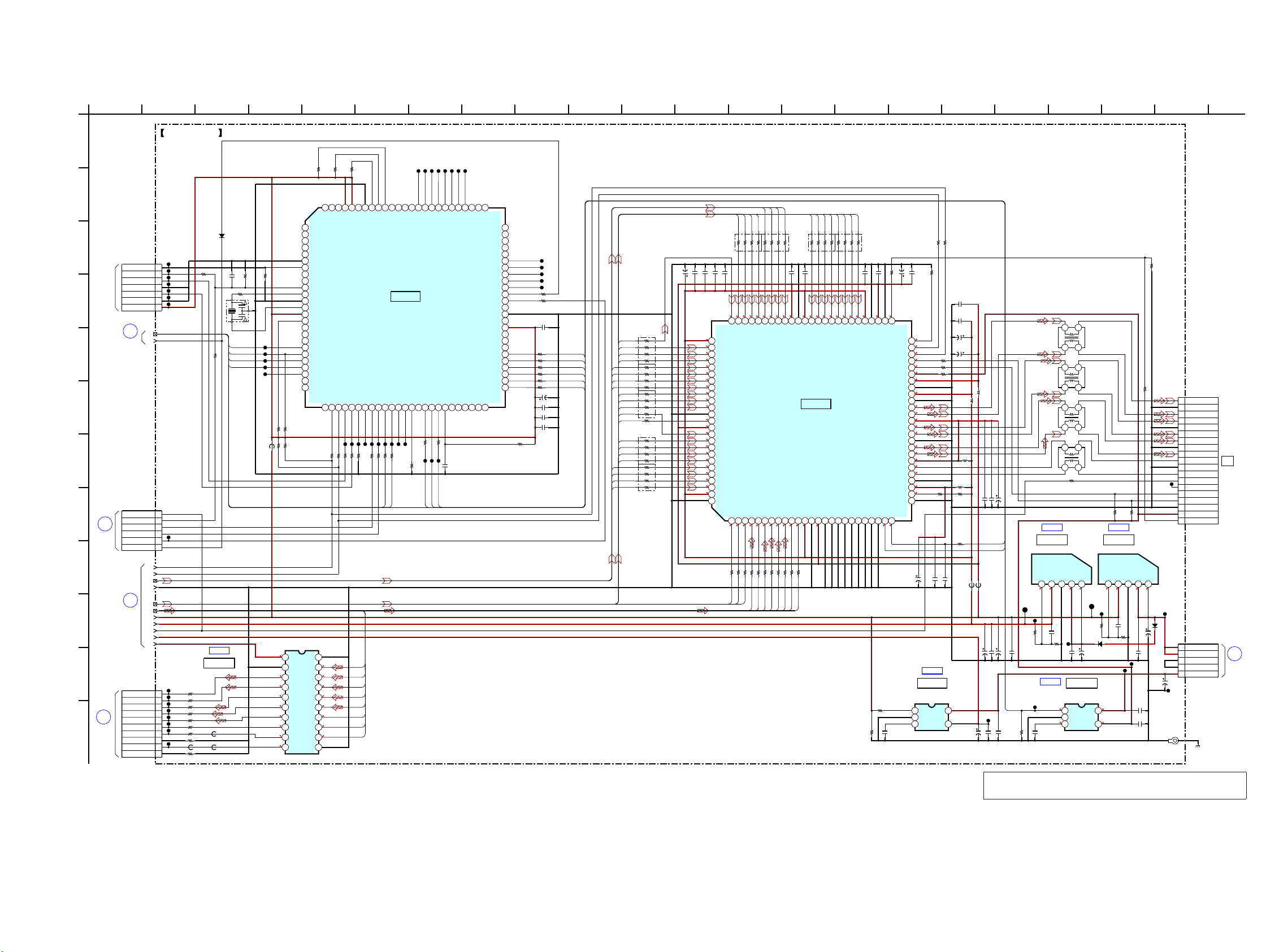
STR-DG820
STR-DG820
2727
11
HDMI
BOARD
(1/2)
IC B/D
S
BOARD
MICOM
CN7003
BOARD
CN4101
DCDC
T
IC B/D
IC B/D
IC B/D IC B/D
12
(1/2)
BOARD
HDMI
BOARD
MICOM
R
CN7002
1.8
0
1.8
2.1
1.2
1.2
1.2
1.2
1.2
1.2
1.2
1.2
1.2
3.3
1.2
1.1
1.2
1.2
1.2
1.2
1.2
1.2
1.2
00000000000
1.8
3.3
3.3
3.3
0
0
1.8
0
0
0
0
0
0
1.8
1.8
1.8
0.2
1.4
1.9
4.9
1.8
3.3
4.9
4.9
0
3.3
1.8
2.1
2.1
2.1
2.1
2.1
2.1
2.1
2.1
2.1
2.1
2.1
2.1
2.1
2.1
2.1
2.1
2.1
1.8
3.3
3.3
0
0
0
0
0
0
0
0
0
0
0
0
0
0
0
0
1.2
3.3
4
4
1.2
1.8
3.2
3.2
3.2
1.3
6
4.9
0.01
C3600
FB3509
10uH
L3504
10uH
L3503
10uH
L3506
0.1
C3568
0.1
C3569
0.1
C3570
100
R3623
680
R3625
10V
100
C3587
10V
100
C3586
10
R3626
10
R3627
47
R3629
JL3526
JL3525
47k
R3640
0R3641
R3634
10k
1.8k
R3638
1.8k
R3639
10V100
C3591
1
C3593
1
C3602
1
C3651
10V100
C3590
1
C3592
10V100
C3603
10V
100
C3604
JL3529
JL3528
47
R3631
4.7k
R3624
47
RB3513
47
RB3512
47
RB3511
47
RB3510
47
RB3515
0R3603
0R3604
0R3605
0R3621
47R3592
0
R3628
HDMI3.3V
123456 789101112131415
16 17 18 19 20 21 22 23 24 25
51525354555657585960616263646566676869707172737475
DE
HSYNC
VSYNC
SPDIF
MCLK
SD3
SD2
SD1
SD0WSSCK
CVCC18
GND
IOVCC33
DCLK
DR0
DL0
DR1
DL1
DR2
DL2
DR3
DL3
INT
RESET#
CVCC18
D18
D17
D16
D15
D14
D13
D12
D11
D10
D9
GND
IDCK
IOVCC33
D8
D7
D6
D5
D4
D3
D2
D1
D0
CVCC18
GND
12345
TK73400AU3G0L-C
IC3511
VCONT
VIN
GND
VOUT
FB
56k
R3632
33kR3635
0.01
C3598
12345
TK73400AU3G0L-C
IC3512
VCONT
VIN
GND
VOUT
FB
47R3606
47R3607
47R3608
47R3609
47R3610
47R3611
47R3612
47R3613
0.01
C3599
3.3k
R3633
6.8k
R3636
JL3527
JL3523
E
ET3502
10MHz
X3000
0.1
C3003
0.1
C3004
FB3000
10V100
C3002
47
R3010
47R3012
47R3018
47R3021
47R3024
47R3025
47
R3027
47
R3036
47
R3031
47
R3035
47
R3030
47
R3034
47
R3033
47R3032
47R3001
10k
R3008
10k
R3004
0.1
C3000
10kR3005
100R3002
10k
R3006
22R3013
22R3014
10k
R3026
10k
R3029
0.1
C3005
0.1
C3006
0.1
C3001
CL3012
CL3013
CL3015
CL3017
CL3019
CL3020
CL3021
CL3022
CL3023
CL3024
CL3025
CL3026
CL3027
CL3016
CL3014
CL3018
CL3011
CL3010
CL3009
CL3008
CL3007
CL3006
CL3005
CL3003
CL3002
CL3004
CL3001
CL3000
0
R3028
1SS367-T3SONY
D3001
JL3524
JL3534
HDMI1.8V
0R3003
0
R3630
5
4
3
2
1
5
4
3
2
1
CONT
GND
NOISE
VOUT
VIN
0.01
C3572
10k
R3622
0.22
C3585
0.22
C3588
EC21QS06-TE12L
D3512
100
R3646
R3023
10k
10k
R3020
R3016
10k
EC21QS06-TE12L
D3511
JL3533
JL3530
JL3535
10kR3037
1
2
3
4
5
5P
CN3507
+4V
+4V
D_GND
BLANK
+6.2V
(NC)
CN3001
47R3038
6P
CN3003
JL3536
JL3537
JL3538
JL3539
JL3540
JL3541
JL3542
CL3028
20
19
18
17
16
15
14
13
12
11
G
A1
A2
A3
A4
A5
A6
A7
A8
GNDY8
Y7
Y6
Y5
Y4
Y3
Y2
Y1
G2
Vcc
JL3543
JL3544
JL3545
JL3546
JL3547
JL3548
JL3549
JL3550
10P
CN3504
100R3596
100
R3593
100
R3597
100
R3595
100R3594
FB3507
FB3506
470R3598
FB3510
0
R3600
0R3602
100
R3599
FB3508
1.5k
R3009
1.5k
R3011
47
RB3509
47
RB3514
47
RB3516
68
RB3517
19P
CN3505
DATA2+
DATA2 SHIELD
DATA2-
DATA1+
DATA1 SHIELD
DATA1-
DATA0+
DATA0 SHIELD
DATA0-
CLOCK+
CLOCK SHIELD
CLOCK-
CEC
RESERVE(NC)
SCL(5V)
SDA(5V)
DDC/CEC GND
+5V POWER
HOT PLUG DET
JL3551
JL3552
26
27
28
29
30
31
32 33
34 35 363738 39
40
41
42 43
44
45 4647484950
767778
79
80
81
8283
84
8586
87
88
8990
91
9293
94
9596
97
98
99
100
NC
NC
NC
NC
NC
BYTE
CNVSS
NC
NC
RESET
XOUT
VSS
XIN
VCC_3.3V
NMI
NC
NC
NC
RX_RST
RX_INT
1444_HPD
HPD_IN1
NC
NC
NC
NC
CSCL
CSDA
232COUT (VU TX)
232CIN (VU RX)NCNC
VUCOM_SDA
VUCOM_SCL
EDID_SELA
EDID_SELBNCNCNCVDAC_RESET
TX_5VPWR
TX_RST
TX_INTNCNCNCNCNCNC
NC
1
4
2 3
FL3500
1
4
2 3
FL3501
1
4
2 3
FL3502
1
4
23
FL3503
0.1
C3571
0.1
C3567
0.1
C3566
0.1
C3564
0.1
C3563
0.1
C3565
0.1
C3573
0.1
C3579
0.1
C3582
0.1
C3578
10V100
C3576
52
51
Q[5]
Q[6]
Q[7]
Q[8]
Q[9]
Q[10]
Q[11]
Q[16]
Q[17]
Q[18]
Q[19]
VSYNC
HSYNC
DE
ODCK
TX_RST
MCK
SD3
SD2
SD1
SD0WSSCK
Q[0]
Q[1]
Q[2]
Q[3]
Q[15]
Q[14]
Q[13]
Q[12]
Q[28]
Q[29]
Q[30]
Q[31]
Q[32]
Q[33]
Q[34]
Q[35]
Q[20]
Q[21]
Q[22]
Q[23]
Q[24]
Q[25]
Q[26]
Q[27]
EDID_MUX_A
EDID_MUX_B
TX_INT
SPDIF
Q[4]
TX_RST
TX_INT
TX_5VPWR
HPD_IN1
RX_RST
1444_HPD
RX_INT
TX_5VPWR
CONT
GND
NOISE VOUT
VIN
HDMI BOARD (2/2)
(CHASSIS)
711
D
21
B
1669 1710
F
5 15
L
K
193
G
201 1812
C
E
H
8
J
4 13
A
142
I
22
232C_IN
232C_OUT
3.3V
RESET
GND
CNVSS
GND
1
2
3
4
5
6
7
BUFFER
IC3507
SPDIF
SD0
SD1
SD2
SD3
LRCK
BCK
GND
MCLK
GND
1
2
3
4
5
6
7
8
9
10
10
9
8
7
6
5
4
3
2
1
IC3507
TC74VHC541FT(EL)
76
77
78
79
80
81
82
83
84
85
86
87
88
89
90
91
92
93
94
95
96
97
98
99
100
HPD
TMODE
IOVCC33
GND
VPP18
D35
D34
D33
D32
D31
D30
D29
D28
CVCC18
GND
IOVCC33
D27
D26
D25
D24
D23
D22
D21
D20
D19
AGND
EXT_SWG
PVCC1
AGND
TXC-
TXC+
AVCC18
TX0-
TX0+
AGND
TX1-
TX1+
AVCC18
TX2-
TX2+
AGND
PVCC2
AGND
AVCC33
DCCPWR5V
DSCL
DSDA
CSCL
CSDA
CI2CA
26
27
28
29
30
31
32
33
34
35
36
37
38
39
40
41
42
43
44
45
46
47
48
49
50
SII9134CTU
IC3508
HDMI TRANSCEIVER
IC3508
0
R3637
OUT
HDMI
1
2
3
4
5
6
7
8
9
10
11
12
13
14
15
16
17
18
19
10V
47
C3608
0.22
C3605
1
C3606
TK11150CSCL-G
IC3510
IC3510
+5V REGULATOR
10V
47
C3589
TK11150CSCL-G
IC3509
IC3509
+5V REGULATOR
10V
47
C3577
+1.8V REGULATOR
IC3512
+3.3V REGULATOR
IC3511
57
59
62
60
56
54
63
58
55
53
61
1
2
3
4
5
6
CEC
HDMI_MICOM_RESET
VUCOM_SDA
VUCOM_SCL
NON_LPCM
HDMI_ERROR
1444_SELA
1444_SELB
1444_SELC
1444_OEB
P5V_SELA
P5V_SELB
NC
NC
NC
VCC_3.3V
NC
VSS
NC
NON LPCM
MUTE
NC
NC
NC
NC
NC
NC
NC
NC
NC
NC
51
52
53
54
55
56
57
58
59
60
61
62
63
64
65
66
67
68
69
70
71
72
73
74
75
NCNCNCNCNCNCNCNCNCNCNCNCNCNCNC
MODEL_SW3
MODEL_SW2
MODEL_SW1
AVSS
NC
VREF
AVCC
NCNCNC
M30620FCPGP U5C
IC3000
IC3000
HDMI CONTROLLER
1
2
3
4
5
6
7
8
9
10
11
12
13
14
15
16
17
18
19
20
21
22
23
24
25
10uH
L3505
10V
47
C3583
10V
47
C3584
0.1
C3581
0.1
C3580
1444_SELA
1444_SELB
1444_SELC
1444_OEB
+5V_SELA
+5V_SELB
MCK
SCK
WS
SD3
SD2
SD1
SD0
SPDIF
• See page 48 for IC Block Diagrams. • See page 56 for IC Pin Function Description.
6-13. SCHEMATIC DIAGRAM - HDMI Board (2/2) -
Note: When IC3508 cannot exchange with single. When IC3508
is damaged, exchange the entire mounted board.
(Page 26)
(Page
37)
(Page
26)
(Page
37)
(Page
45)
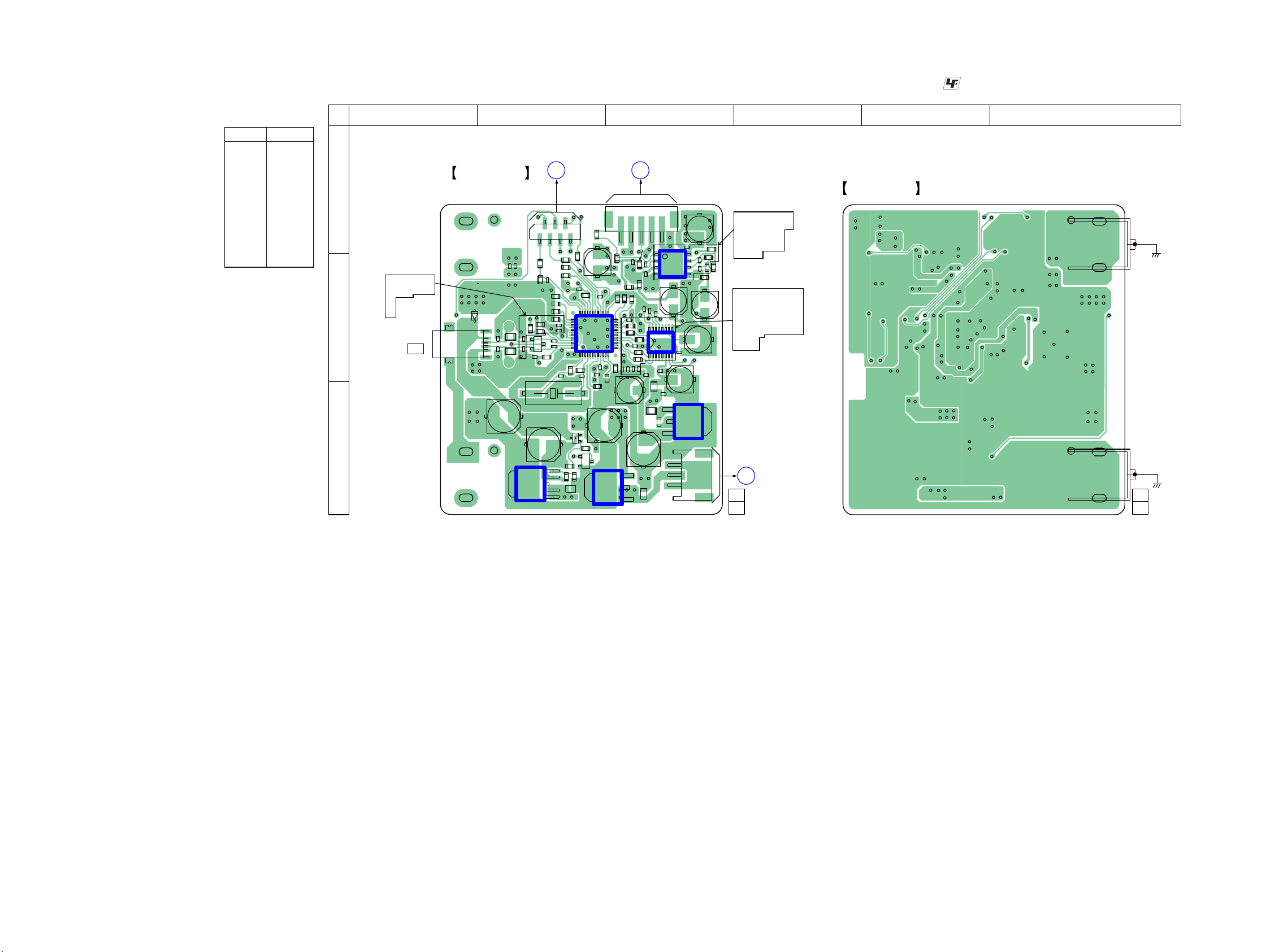
STR-DG820
STR-DG820
2828
1
8
9
16
1
3
2
1
7
6
1
5
EP101
EP102
Q105
Q106
L101
L102
FB101
FB104
R101
R102
R103
R104
R107
R108
R109
R110
R112
R115
R116
R117
R118
R119
CN101
CN102
R120
R121
R123
R124
R126
R127
R128
R130
R131
R132
R133
R137
R138
C101
C102
C103
C104
R143
R144
C108
R145
R146
R147
C110
C111
X101
12
1
13
48
36
37
24
25
C113
C118
C119
R156
R158
C120
C121
C122
C123
C124
C125
R162
C126
R163
C127
C128
C129
C130
C131
C132
C133
C134
C135
C136
C137
C138
R174
C139
R176
C140
C142
C143
C144
C145
C153
C157
C159
D101
C161
C163
D103
C164
C165
C166
C174
C175
C176
IC101
IC102
IC104
IC105
IC106
IC107
CNP103
J101
E
E
C105
C106
C107
C109
R122
R125
C116
R129
R134
1
45
8
XM BOARD
(COMPONENT SIDE)
XM BOARD (CONDUCTOR SIDE)
(CHASSIS)
(CHASSIS)
1
4
A
K
XM
K
D
MAIN
BOARD
CN434
U
MICOM
BOARD
CN7013
V
DCDC
BOARD
CN4101
1-875-744-
11
(11)
1-875-744-
11
(11)
1
4
5
2
3
1
3
2
3
1
2
+
+
+
+
+
+
+
+
+
+
+
A
B
C
12345 6
6-14. PRINTED WIRING BOARD - XM Board (US, Canadian models) -
• : Uses unleaded solder.
• See page 19 for Circuit Boards Location.
(Page 36)
(Page 20)
(Page 45)
Ref. No. Location
• Semiconductor
Location
D101 B-2
D103 B-1
IC101 C-3
IC102 B-2
IC104 B-3
IC105 B-3
IC106 C-2
IC107 C-3
Q105 C-2
Q106 C-2
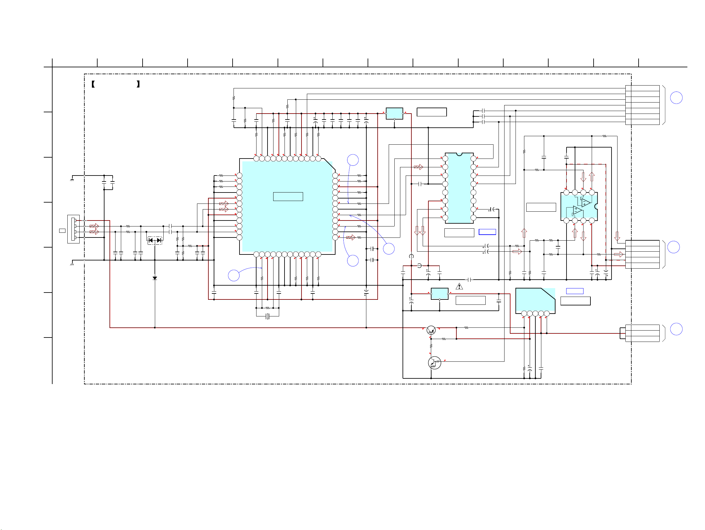
STR-DG820
STR-DG820
2929
• See page 48 for Waveforms. • See page 48 for IC Block Diagrams. • See page 56 for IC Pin Function Description.
6-15. SCHEMATIC DIAGRAM - XM Board (US, Canadian models) -
MICOM
U
BOARD
CN7013
BOARD
(2/3)
D
CN434
MAIN
IC B/D
IC B/D
11
12
13
14
BOARD
DCDC
CN4101
V
0
3.2
3.3
3.3
0
3.3
3.3
3.3
3.3
0
0
3.3
3.3
1.2
1.2
3.3
1.2
1.2
3.3
0
3.3
0
1.7
1.7
3.3
1.7
0
1.6
3.3
1.6
0
3.3
0
3.3
3.3 5
1.71. 7
0
1.7
5
2.5
2.5
3.3
0
2.5
0
56.3
1.3
5.3
6.3
6.3
5.3 5.3
3.2
0.1
5.3
7
0
0
0
0
-6.9
47kR122
47kR145
FB101
4P
J101
1
2
3
4
16
15
14
13
12
11
10
98
7
6
5
4
3
2
1
PCM1753DBQR
IC105
100kR102
0
L102
47kR118
100R108
10kR115
47kR146
100R107
10kR147
10k
R103
4.7k
R158
100k
R101
FB104
47kR121
100k
R128
VCC
GND
OUT
BA33BC0FP-E2
IC101
1
3
2
4321
5678
NJM4565M(TE2)
IC104
10kR116
100
R130
220R125
45.1584MHz
X101
12k
R120
680
R123
1kR138
100
R131
10k
R104
680
R133
10k
R112
100R127
0.47
C161
KDS160-RTK
D103
VCC
GND
OUT
BA50BC0FP-E2
IC107
13
2
680
R174
12k
R137
100
R110
0.47
C157
0.47
C102
150R156
47kR109
100R129
0
L101
8.2k
R124
NSAD500F-T1B
D101
100
R143
100kR126
1kR144
8.2k
R132
100
R134
DTC114YKA-T146
Q105
10k
R176
47kR119
100
R117
12345
BA00BC0WFP-E2
IC106
16V
100
C101
16V
100
C159
50V10
C104
50V
10
C122
50V
10
C125
16V
100
C145
16V100C153
50V
10
C137
50V
10
C113
50V
10
C142
50V
10
C139
0.1
C103
0.1
C108
0.1
C105
0.1
C110
0.1
C123
0.1
C121
0.1
C111
0.1
C116
0.1
C124
0.1
C138
0.1
C140
0.1
C127
0.1
C126
0.1
C136
0.1
C130
0.1
C119
0.1
C144
0.1
C143
1000p
C107
1000p
C109
1000p
C106
5p
C166
5p
C165
22pC131
22pC132
22pC134
22pC133
100p
C174
100p
C176
100p
C175
680p
C118
680p
C129
6800pC120
6800p
C128
0.01
C135
0.1
C164
0.1
C163
1
2
3
3P
CNP103
13
14
15
16
17
18
19
20
21
22
23
24
25 26 27 28
29 30 31 32 33 34 35 36
12 11 10 9 87654321
37
38
39
40
41
42
43
44
45
46
47
48
F2602E-01-TR
IC102
LSOPTXRX
VSS
SCTXOUT
VDD
SCRXIN
VSS
COMMSEL
VDD
IRQ*
VSS
RESET*
SLAVESL
COMRXDIG
COMTXDIG
COMTXEN
VSS
VDD
COMRXP
COMRXM
VDD
VSS
COMTXM
COMTXP
VSS
VSS
OSCOUT
VDD
OSCIN
VSS
TEST
VSS
HSDPDATA
VDD
HSDPCLK
VSS
HSDPEN
I2SDATA
VSS
I2SSCLK
VDD
I2SLRCLK
VSS
I2SOCLK
VSS
SAIICLK
VDD
SAIIDATA
SAIIEN
2SB1689-T106
Q106
1
2
3
4
5
6
7
7P
CN101
100k
R162
330k
R163
1
2
3
4
5
5P
CN102
VCOM
XM_DACMS
ZEROL
MC
DGND
VOUTR
AGND
XM_MOXMI
VOUTL
BCK
DATA*
6.3VDC
ML(MS)
LRCK
XM_RESET
DGND
XMDAC_MC
VCC(5V)
ZEROR
DGND
XM_DBPOWER
XMDAC_MDI
MD(MDI )
XM_MIXMO
NC
SCK
XMR
XMGND
XML
-7V
+7V
+5V REGULATOR
IC107
+5.3V REGULATOR
IC106
IC104
LINE AMP
IC105
D/A CONVERTER
IC102
XM RECEIVER
IC101
+3.3V REGULATOR
XM BOARD
EP101
(CHASSIS)
(CHASSIS)
EP102
VCC
VEE
NC
OUT
GND
VCC
CTL
B+ SWITCH
Q105, 106
XM
D
B
10 11
F
53
G
1 12
C
E
89674 13
A
142
(Page 37)
(Page 22)
(Page 45)
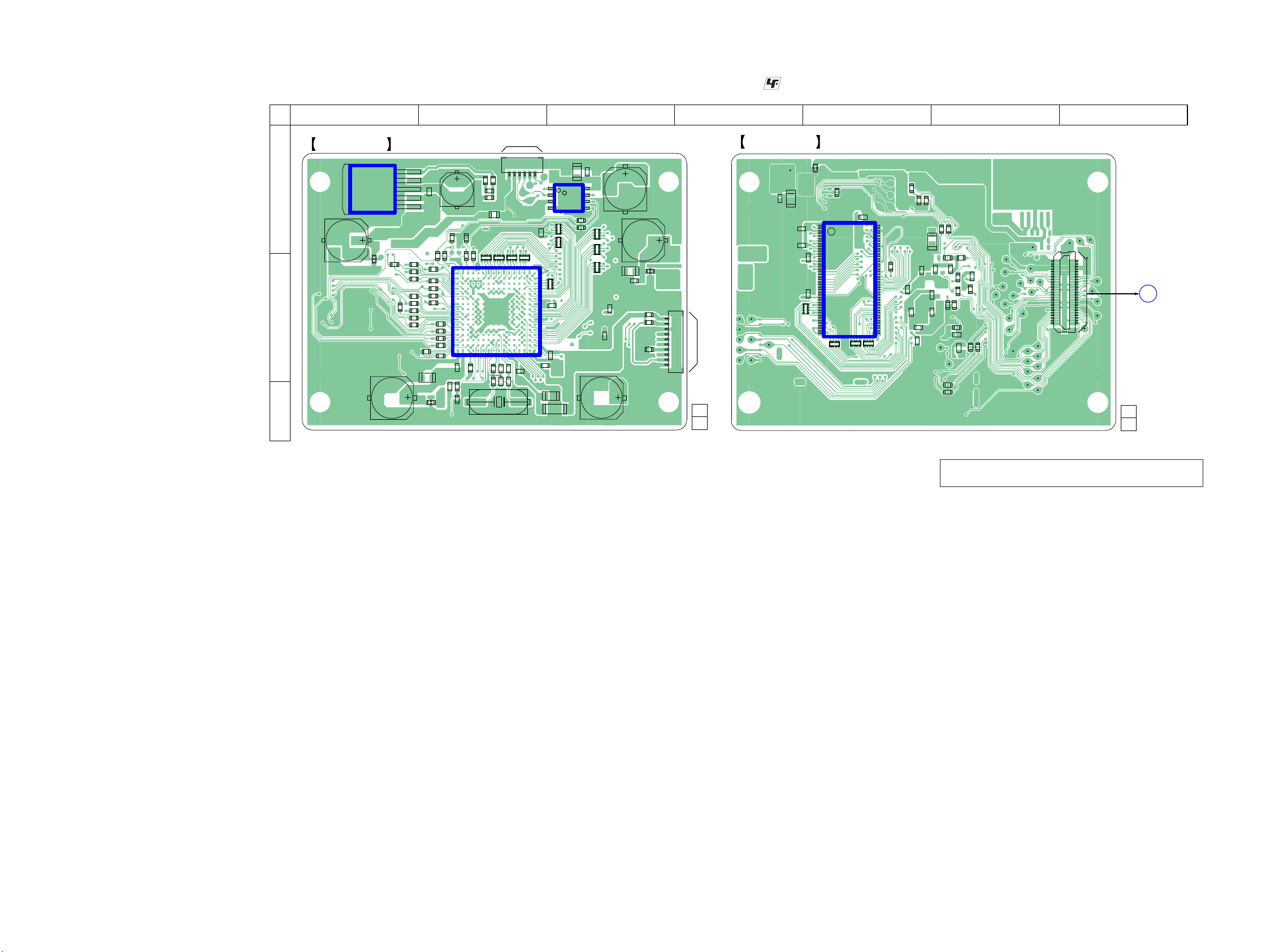
STR-DG820
STR-DG820
3030
R5358
R5359
CN5002
C5199
R5368
R5369
R5375
R5376
R5377
R5384
R5385
R5387
X002
R5397
R5365
R5363
CN5003
C5001
C5007
C5200
C5201
C5012
R5402
R5403
IC5015
IC5020
R5411
IC5021
R5413
C5088
C5091
C5094
C5095
FL5006
FL5009
FL5011
FL5013
R5279
R5280
C5117
FB5003
RB009
RB011
C5132
RB015
RB016
RB019
RB021
RB022
RB024
R5379
R5002
RB025
RB026
R5321
R5322
R5323
R5324
R5325
R5326
R5327
C5161
C5162
C5163
C5164
R5331
C5165
R5332
C5166
R5333
R5334
C5168
R5335
R5336
R5337
C5170
C5172
C5173
R5341
C5178
R5347
R5349
C5181
R5350
C5185
C5188
R5355
R5357
C5195
C5196
C5197
C5198
CL5001
CL5002
CL5003
CL5004
CL5005
R5373
R5378
R5386
R5391
R5392
R5393
R5394
R5399
CL5036
CL5044
CL5045
CL5046
CL5047
CL5048
CN5001
CL5051
CL5052
CL5059
C5202
CL5062
R5404
R5405
R5406
R5407
R5410
R5412
IC5022
R5414
FL5010
CL5102
CL5104
CL5105
CL5107
CL5108
CL5109
CL5110
CL5111
CL5112
CL5113
CL5114
CL5115
CL5116
CL5117
CL5118
R5290
CL5120
CL5121
R5299
CL5139
CL5152
CL5153
CL5156
CL5157
CL5158
CL5159
CL5160
CL5161
CL5162
CL5163
CL5164
CL5165
CL5166
C5120
C5126
RB010
RB012
RB013
RB014
C5139
C5140
C5144
C5150
C5155
C5175
C5176
C5177
C5179
R5346
R5348
C5180
C5182
C5183
C5189
1
10
1
8
5
4
1-875-772-
(NC)
(NC)
11
(11)
DSP BOARD (SIDE A)
1
1
2
49
50
43
44
86
1-875-772-
11
(11)
DSP BOARD (SIDE B)
X
DIGITAL
AUDIO
BOARD
CN2206
A
B
C
1234567
1
5
A16B16 C16D16 E16 F16 G16H16 J16 K16 L16M16 N16P16 R16 T16
A15B15 C15D15 E15 F15 G15H15 J15 K15 L15M15 N15P15 R15 T15
A14B14 C14D14 E14 F14 G14H14 J14 K14 L14M14 N14P14 R14 T14
A13B13 C13D13 E13 F13 G13H13 J13 K13 L13M13 N13P13 R13 T13
A12B12 C12D12 E12 F12 G12H12 J12 K12 L12M12 N12P12 R12 T12
A11B11 C11D11 E11 F11 G11H11 J11 K11 L11M11 N11P11 R11 T11
A10B10 C10D10 E10 F10 G10H10 J10 K10 L10M10 N10P10 R10 T10
A9 B9 C9 D9 E9 F9 G9 H9 J9 K9 L9 M9 N9 P9 R9 T9
A8 B8 C8 D8 E8 F8 G8 H8 J8 K8 L8 M8 N8 P8 R8 T8
A7 B7 C7 D7 E7 F7 G7 H7 J7 K7 L7 M7 N7 P7 R7 T7
A6 B6 C6 D6 E6 F6 G6 H6 J6 K6 L6 M6 N6 P6 R6 T6
A5 B5 C5 D5 E5 F5 G5 H5 J5 K5 L5 M5 N5 P5 R5 T5
A4 B4 C4 D4 E4 F4 G4 H4 J4 K4 L4 M4 N4 P4 R4 T4
A3 B3 C3 D3 E3 F3 G3 H3 J3 K3 L3 M3 N3 P3 R3 T3
A2 B2 C2 D2 E2 F2 G2 H2 J2 K2 L2 M2 N2 P2 R2 T2
A1 B1 C1 D1 E1 F1 G1 H1 J1 K1 L1 M1 N1 P1 R1 T1
6-16. PRINTED WIRING BOARD - DSP Board -
• : Uses unleaded solder.
• See page 19 for Circuit Boards Location.
(Page 32)
Note: When IC5021 cannot exchange with single. When IC5021
is damaged, exchange the entire mounted board.
 Loading...