

Sony STRDG-810 Service manual
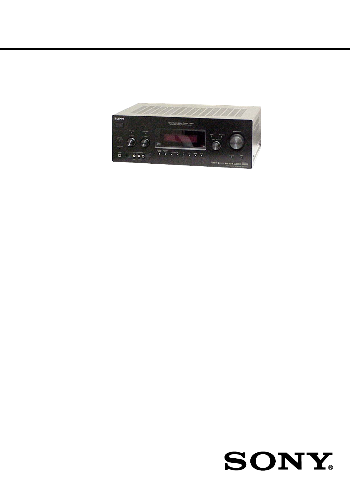
STR-DG810
SERVICE MANUAL
Ver. 1.0 2007. 03
This receiver incorporates Dolby* Digital and Pro
Logic Surround and the DTS** Digital Surround
System.
* Manufactured under license from Dolby
Laboratories.
“Dolby”, “Pro Logic”, “Surround EX”, and the
double-D symbol are trademarks of Dolby
Laboratories.
** “DTS” and “DTS-ES | Neo:6” are registered
trademarks of DTS, Inc. “96/24” is a trademark
of DTS, Inc.
This receiver incorporates High-Definition
Multimedia Interface (HDMITM) technology.
HDMI, the HDMI logo and High-Definition
Multimedia Interface are trademarks or registered
trademarks of HDMI Licensing LLC.
XM is a registered trademark of XM Satellite Radio
Inc.
This product is manufactured under license from
Neural Audio Corporation.
Sony Corporation hereby grants the used a nonexclusive, non-transferable, limited license right to
use this product under the US and foreign patents
pending and other related technology owned by
Neural Audio Corporation.
SPECIFICATIONS
AUDIO POWER SPECIFICATIONS
POWER OUTPUT AND TOTAL HARMONIC
DISTORTION:
(Models of area code US only)
With 8 ohm loads, both channels driven, from
20 – 20,000 Hz; rated 100 watts per channel
minimum RMS power, with no more than
0.09 % total harmonic distortion from 250
milliwatts to rated output.
Amplifier section
Models of area code US
Minimum RMS Output Power (8 ohms, 20 Hz –
20 kHz, THD 0.09%)
Stereo Mode Output Power (8 ohms, 1 kHz,
THD 1%)
Surround Mode Output Power
THD 10%)
1)
100 W + 100 W
110 W + 110 W
2)
150 W/ch
(8 ohms 1 kHz,
– Continued on next page –
US Model
“Neural” and “Neural Audio” and “Neural
Surround” are trademarks of Neural Audio
Corporation.
9-887-624-01
2007C04-1
© 2007. 03
Sony Corporation
Home Audio Division
Published by Sony Techno Create Corporation
MULTI CHANNEL AV RECEIVER
1

STR-DG810
1) Measured under the following conditions:
Area code Power requirements
US 120 V AC, 60 Hz
2) Reference power output for front, center, surround and
surround back speakers. Depending on the sound field
settings and the source, there may be no sound output.
Frequency response
Analog 10 Hz – 70 kHz
Inputs
Analog Sensitivity: 500 mV/
Digital (Coaxial) Impedance: 75 ohms
Digital (Optical) S/N: 100 dB
Output (Analog)
AUDIO OUT Voltage: 500 mV/10 kohms
SUB WOOFER Voltage: 2 V/1 kohm
Equalizer
Gain levels ±10 dB, 1 dB step
3) INPUT SHORT (with sound field and equalizer
bypassed).
4) Weighted network, input level.
+0.5/–2 dB (with sound
field and equalizer bypassed)
50 kohms
3)
S/N
: 96 dB
(A, 500 mV
S/N: 100 dB
(A, 20 kHz LPF)
(A, 20 kHz LPF)
4)
)
FM tuner section
Tuning range 87.5 – 108.0 MHz
Antenna FM wire antenna
Antenna terminals 75 ohms, unbalanced
Intermediate frequency 10.7 MHz
AM tuner section
Tuning range
Models of area code US
With 10-kHz tuning scale: 530 – 1,710 kHz
With 9-kHz tuning scale: 531 – 1,710 kHz
Antenna Loop antenna
Intermediate frequency 450 kHz
5) You can change the AM tuning scale to 9 kHz or 10 kHz.
After tuning in any AM station, turn off the recei ver . While
holding down TUNING MODE, press ?/1. All preset
stations will be erased when you change the tuning scale.
To reset the scale to 10 kHz (or 9 kHz), repeat the
procedure.
5)
5)
General
Power requirements
Area code Power requirements
US 120 V AC, 60 Hz
Power output (DIGITAL MEDIA PORT)
DC OUT 5 V, 700 mA
Power consumption
Area code Power consumption
US 250 W
Power consumption (during standby mode)
0.3 W (When “CONTROL”
in VIDEO menu is set to
“CTRL OFF”)
AC outlets:
Area code AC outlets
US 1 switch, 120 W/1A MAX
Dimensions (w/h/d) (Approx.)
430 × 157.5 × 316 mm
(16 7/8 × 6 2/8 × 12 4/8
inches) including
projecting parts and
controls
Mass (Approx.) 8.1 kg (17 lb 14 oz)
Supplied accessories
FM wire antenna (1)
AM loop antenna (1)
Remote commander RM-AAP016 (1)
R6 (size-AA) batteries (2)
Optimizer microphone ECM-AC2 (1)
Design and specifications are subject to change
without notice.
Video section
Inputs/Outputs
Video: 1 Vp-p/75 ohms
COMPONENT VIDEO: Y: 1 Vp-p/75 ohms
PB/CB: 0.7 Vp-p/
75 ohms
PR/CR: 0.7 Vp-p/
75 ohms
80 MHz HD Pass Through
2
STR-DG810
SAFETY CHECK-OUT (US MODEL)
After correcting the original service problem, perform the following safety check before releasing the set to the customer:
Check the antenna terminals, metal trim, “metallized” knobs, screws,
and all other exposed metal parts for AC leakage.
Check leakage as described below.
LEAKAGE TEST
The AC leakage from any exposed metal part to earth ground and
from all exposed metal parts to any exposed metal part having a
return to chassis, must not exceed 0.5 mA (500 microampers.).
Leakage current can be measured by any one of three methods.
1. A commercial leakage tester, such as the Simpson 229 or RCA
WT-540A. Follow the manufacturers’ instructions to use these
instruments.
2. A battery-operated AC milliammeter. The Data Precision 245
digital multimeter is suitable for this job.
3. Measuring the voltage drop across a resistor by means of a
VOM or battery-operated AC voltmeter. The “limit” indication is 0.75 V, so analog meters must have an accurate lowvoltage scale. The Simpson 250 and Sanwa SH-63Trd are examples of a passive VOM that is suitable. Nearly all battery
operated digital multimeters that have a 2 V A C range are suitable. (See Fig. A)
To Exposed Metal
Parts on Set
MODEL IDENTIFICATION
— BACK PANEL —
Part No.
MODEL PART No.
US 2-898-468-0s
NOTE OF REPLACING THE IC3511 AND IC3513 ON THE
HDMI RE BOARD
When IC3511 and IC3513 on the HDMI RE board are damaged,
exchange the new HDMI RE board for the HDMI RE board which
IC damaged. When throwing aw ay the HDMI RE board, be sure to
throw away after destroying IC3511 and IC3513 physically with
the hammer etc.
AC
0.15 µF
1.5 k
Ω
Earth Ground
voltmeter
(0.75 V)
Fig. A. Using an AC voltmeter to check AC leakage.
SAFETY-RELATED COMPONENT WARNING!!
COMPONENTS IDENTIFIED BY MARK 0 OR DOTTED LINE
WITH MARK 0 ON THE SCHEMATIC DIAGRAMS AND IN
THE PARTS LIST ARE CRITICAL TO SAFE OPERATION.
REPLACE THESE COMPONENTS WITH SONY P ARTS WHOSE
PART NUMBERS APPEAR AS SHOWN IN THIS MANUAL OR
IN SUPPLEMENTS PUBLISHED BY SONY.
3

STR-DG810
TABLE OF CONTENTS
1. GENERAL
Description and location of parts............................................. 5
2. DISASSEMBLY
2-1. Case .....................................................................................8
2-2. Back Panel Section.............................................................. 9
2-3. Front Panel Section ............................................................. 9
2-4. DIGITAL Board ................................................................ 10
2-5. MAIN Board Section ........................................................ 10
2-6. STANDBY Board ............................................................. 11
3. TEST MODE ..................................................................... 12
4. FM TUNER CHECK ....................................................... 13
5. DIAGRAMS
5-1. Block Diagram – Tuner/Audio Section –.......................... 15
5-2. Block Diagram – Digital Section – ................................... 16
5-3. Block Diagram – Video Section – ..................................... 17
5-4. Block Diagram – HDMI SW Section –............................. 18
5-5. Block Diagram – XM Section –........................................19
5-6. Block Diagram – Key/Display Section – .......................... 20
5-7. Block Diagram – Power Section – .................................... 21
5-8. Printed Wiring Boards – Main Section – .......................... 23
5-9. Schematic Diagram – Main Section (1/2) – ...................... 24
5-10. Schematic Diagram – Main Section (2/2) – ...................... 25
5-11. Printed Wiring Board – Digital Section (1/2) – ................ 26
5-12. Printed Wiring Board – Digital Section (2/2) – ................ 27
5-13. Schematic Diagram – Digital Section (1/5) – ................... 28
5-14. Schematic Diagram – Digital Section (2/5) – ................... 29
5-15. Schematic Diagram – Digital Section (3/5) – ................... 30
5-16. Schematic Diagram – Digital Section (4/5) – ................... 31
5-17. Schematic Diagram – Digital Section (5/5) – ................... 32
5-18. Printed Wiring Board – Video Section – ........................... 33
5-19. Schematic Diagram – Video Section –.............................. 34
5-20. Printed Wiring Board – HDMI RE Section (1/2) –........... 35
5-21. Printed Wiring Board – HDMI RE Section (2/2) –........... 36
5-22. Schematic Diagram – HDMI RE Section (1/2) –.............. 37
5-23. Schematic Diagram – HDMI RE Section (2/2) –.............. 38
5-24. Printed Wiring Board – XM Section – .............................. 39
5-25. Schematic Diagram – XM Section –................................. 40
5-26. Printed Wiring Boards – DCAC, Power Key Section – .... 41
5-27. Schematic Diagram – DCAC, Power Key Section – ........41
5-28. Printed Wiring Board – Display Section – ........................ 42
5-29. Schematic Diagram – Display Section –........................... 43
5-30. Printed Wiring Board – Power Section – .......................... 44
5-31. Schematic Diagram – Power Section – ............................. 44
5-32. Printed Wiring Board – DCDC Section – ......................... 45
5-33. Schematic Diagram – DCDC Section – ............................ 45
6. EXPLODED VIEWS
6-1. Case Section ...................................................................... 60
6-2. Front Panel Section ........................................................... 61
6-3. Back Panel Section............................................................ 62
6-4. Chassis Section ................................................................. 63
7. ELECTRICAL PARTS LIST ........................................ 64
4
SECTION 1
6
US
Name Function
J DIRECT Press to listen to high
quality analog sound (page
57).
K AUTO CAL Press to activate the Auto
Calibration function
(page 30).
L INPUT
SELECTOR
Turn to select the input
source to playback (page
35, 37, 38, 57, 59, 64, 71,
74, 76, 78).
M MOVIE Press to select a sound field
(page 52, 54, 57).
MUSIC
A.F.D.
2CH
N CATEGORY +/– Used when listening to XM
Radio (page 66).
CATEGORY
MODE
O VIDEO 3 IN/
PORTABLE AV
IN jacks
Connect to a camcorder or
video game (page 25, 36).
P PHONES jack Connects to headphones
(page 87).
Q AUTO CAL MIC
jack
Connects to the supplied
optimizer microphone for
the Auto Calibration
function (page 29).
8
US
Name Function
G DTS/
DTS-ES/
DTS 96/24
“DTS” lights up when DTS
signals are input. “DTS-ES”
lights up when DTS-ES signals
are input.
“DTS 96/24” lights up when the
receiver is decoding DTS 96
kHz/24 bit signals.
Note
When playing a DTS format
disc, be sure that you have made
digital connections and that
INPUT MODE is not set to
“ANALOG” (page 71).
H CAT Lights up when you select
category mode to “ONE CAT”.
For details on presetting XM
Radio station, see page 68.
I MEMORY Lights up when a memory
function, such as Preset
Memory (page 61), etc., is
activated.
J Tun er
indicators
Lights up when using the
receiver to tune in radio stations
(page 58), etc.
K Preset
station
indicators
Lights up when using the
receiver to tune in radio stations
you have preset. For details on
presetting radio stations, see
page 60.
L D.RANGE Lights up when dynamic range
compression is activated
(page 40).
M NEO:6 Lights up when DTS Neo:6
Cinema/Music decoder is
activated (page 53).
N COAX Lights up when INPUT MODE
is set to “AUTO IN” and the
source signal is a digital signal
being input through the
COAXIAL jack, or when
INPUT MODE is set to “COAX
IN” (page 71).
O HDMI Lights up when the receiver
recognizes a component
connected via an HDMI IN jack
(page 19).
Name Function
P Playback
channel
indicators
L
R
C
SL
SR
S
SB
The letters (L, C, R, etc.)
indicate the channels being
played back. The boxes around
the letters vary to show how the
receiver downmixes the source
sound (based on the speaker
settings).
Front Left
Front Right
Center (monaural)
Surround Left
Surround Right
Surround (monaural or the
surround components obtaine d
by Pro Logic processing)
Surround back (the surround
back components obtained by
6.1 channel decoding)
Example:
Recording format (Front/
Surround): 3/2.1
Output channel: When surround
speakers are set to “NO”
(page 42)
Sound Field: A.F.D. AUTO
SW
LC
SL
R
SR
GENERAL
STR-DG810
This section is extracted
from instruction manual.
Getting Started
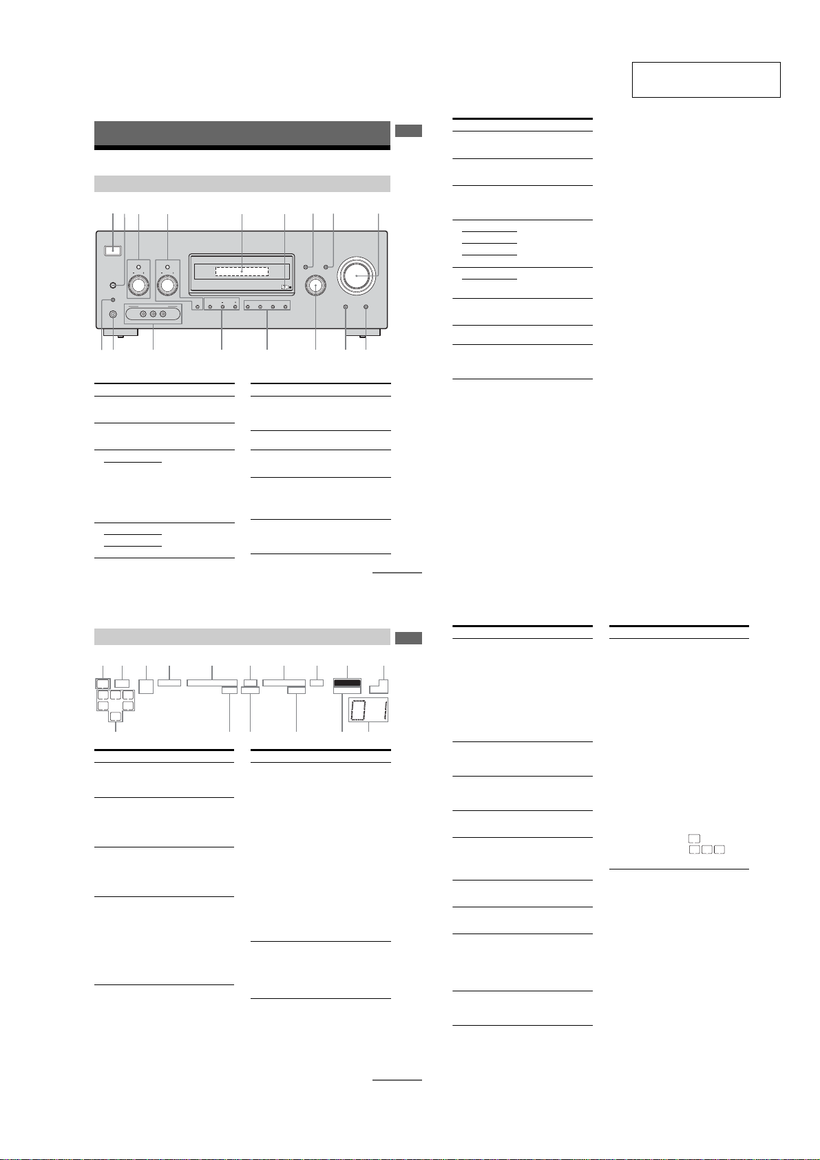
Description and location of parts
Front panel
2 9578
1
3 4
?/1
SPEAKERS
(OFF/A/B/A+B)
AUTO CAL MIC
PHONES
TONE MODE
TONE
VIDEO 3 IN/PORTABLE AV IN
VIDEO L AUDIO R
TUNING MODE
TUNING
MEMORY/
CATEGORY
CATEGORY
ENTER
MODE
qj qdqfqgqh qs
Name Function
A ?/1
(on/standby)
B SPEAKERS
(OFF/A/B/A+B)
C TONE MODE Adjusts the tonal quality
TONE +/–
D TUNING MODE Press to operate a tune r
TUNING +/–
MEMORY/ENTER
Press to turn the receiver
on or off (page 27, 37, 38,
58, 91).
Press to select OFF, A, B,
A+B of the front speakers
(page 28).
(bass/treble level) of the
front speakers.
Press TONE MODE
repeatedly to select
“BASS LVL” or “TRE
LVL”, then turn TONE
+/– to adjust the level
(page 40).
(FM/AM/XM) (page 58,
63).
6
DISPLAY INPUT MODE
INPUT SELECTOR
2CH A.F.D. MOVIE MUSIC
Name Function
E Display The current status of the
F Remote sensor Receives signals from
G DISPLAY Press to select information
H INPUT MODE Press to select the input
I MASTER
VOLUME
selected component or a
list of selectable items
appears here (page 7).
remote commander.
displayed on the display
(page 67, 77).
mode when the same
components are connected
to both digital and analog
jacks (page 71).
Turn to adjust the volume
level of all speakers at the
same time (page 34, 36, 37,
38).
MASTER VOLUME
AUTO CAL DIRECT
qa
continued
Getting Started
q;
US
5
About the indicators on the display
1 2 3 4 5 6 7 8 q;9
LFE
SW
R
LC
SR
SL S
SB
Name Function
A SW Lights up when sub woofer is
B LFE Lights up when the disc being
C SP A/SP B Lights up according to the
D ; D/
; D EX
SP A
D EX;PL IIx;PL OPT DTS -ES CAT96/24 MEMORY ST
;
SP B
set to “YES” (page 42) and the
audio signal is output from the
SUB WOOFER jack.
played back contains an LFE
(Low Frequency Effect)
channel and the LFE channel
signal is actually being
reproduced.
speaker system used. However,
these indicators do not l ight up
if the speaker output is turned
off or if headphones are
connected.
“; D” lights up when Dolby
Digital signals are input. “; D
EX” lights up when Dolby
Digital Surround EX signals are
decoded.
Note
When playing a Dolby Digital
format disc, be sure that you
have made digital connections
and that INPUT MODE is not
set to “ANALOG” (page 71).
Name Function
E ; PL/
; PL II/
; PL IIx
F OPT Lights up when INPUT MODE
“; PL” lights up when the
receiver applies Pro Logic
processing to 2 channel signals
in order to output the center and
surround channel signals.
“; PL II” lights up when the
Pro Logic II Movie/Music/
Game decoder is activated.
“; PL IIx” lights up when the
Pro Logic IIx Movie/Music/
Game decoder is activated.
However, these indicators do
not light up if both the center
and surround speakers are s et to
“NO” (page 42) and you select a
sound field using the A.F.D.
button.
Note
Dolby Pro Logic IIx decoding
does not function for DTS
format signals or for signals
with a sampling frequency of
more than 48 kHz.
is set to “AUTO IN” and the
source signal is a digital signal
being input through the
OPTICAL jack, or when
INPUT MODE is set to “OPT
IN” (page 71).
continued
Getting Started
MONOD.RANGECOAXHDMI NEO:6
qaqsqh qfqg qd
US
7
5
STR-DG810
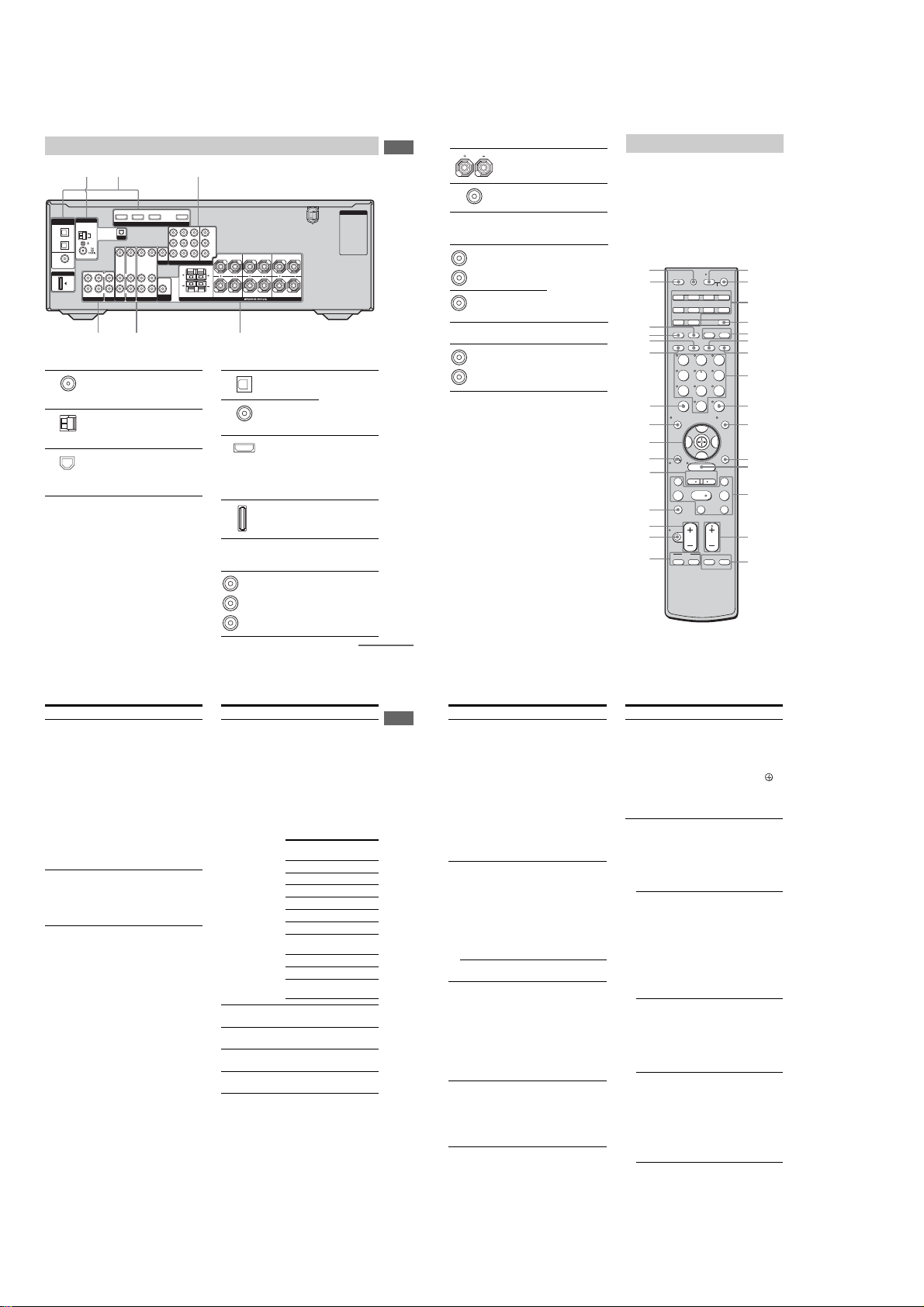
Rear panel
2 3
1
DIGITAL
ANTENNA
(ASSIGNABLE)
OPTICAL
SAT
IN
AM
VIDEO 1
IN
COAXIAL
DVD
IN
DMPORT
A ANTENNA section
VIDEO IN
L
R
R
OUT IN IN
AUDIO IN
SA-CD/CD/CD-R
TV
SAT
FM
ANTENNA
jack
AM
ANTENNA
terminals
XM jack Connects to the XM
SAT IN DVD IN VIDEO 2/BD IN OUT
HDMI
XM
VIDEO OUT
SAT IN
VIDEO IN
VIDEO OUT
VIDEO IN
MONITOR
LRL
L
AUDIO OUT
R
AUDIO IN
AUDIO OUT
AUDIO IN
SUB
WOOFER
DVD
VIDEO 1
Connects to the FM
wire antenna
supplied with this
receiver (page 26).
Connects to the AM
loop antenna
supplied with this
receiver (page 26).
Connect-and-Play
antenna (not
supplied with this
receiver) (page 63).
DVD IN VIDEO 1 IN
COMPONENT VIDEO
FRONT B
Y
P
B/CB
PR/C
MONITOR OUT
LLR
R
SPEAKERS
FRONT A
R
SURROUND
SURROUND BACK
L
R
CENTER
456
B DIGITAL INPUT/OUTPUT section
OPTICAL
IN jack
COAXIAL
IN jack
HDMI IN/
OUT jack*
DMPORT Connects to a
C COMPONENT VIDEO INPUT/
OUTPUT section
COMPONENT
Green
VIDEO
(Y)
INPUT/
Blue
OUTPUT
(P
B/CB
)
jack*
Red
(P
R/CR
)
AC OUTLET
Connects to a
DVD player, etc.
The COAXIAL
jack provides a
better quality of
loud sound (page
22, 24).
Connects to a
DVD player or a
satellite tuner, etc.
The image and the
sound are output to
TV or a projector
(page 19).
DIGITAL MEDIA
PORT adapter
(page 73).
Connects to a
DVD player, TV
or a satellite tuner,
etc. You can enjoy
high quality image
(page 21 – 24).
continued
D SPEAKER section
Getting Started
E VIDEO/AUDIO INPUT/OUTPUT
section
AUDIO IN/
White (L)
OUT jack
Red (R)
VIDEO IN/
Yellow
OUT jack*
Connects to
speakers (page 16).
Connects to sub
woofer (page 16).
Connects the video
and audio jacks of a
VCR or a DVD
player (page 21 –
25).
F AUDIO INPUT/OUTPUT section
AUDIO IN/
White (L)
OUT jack
Red (R)
*You can watch the selected input image when you
connect the MONITOR OUT jack to a TV mo nitor
(page 21).
US
9
US
10
Connects to a
Super Audio CD
player or CD
player, etc. (page
17).
Remote commander
You can use the supplied remote to operate the
receiver and to control the Sony audio/video
components that the remote is assigned to
operate. You can also program the remote to
control non-Sony audio/vi deo components.
For details, see “Programming the remote”
(page 79).
RM-AAP016
e;
wl
wk
wj
wh
wg
wf
wd
ws
wa
w;
ql
qk
qj
qh
TV
RM SET UP
VIDEO 1 VIDEO 2 VIDEO 3 DVD
SAT TV TUNER
AUX DMPORT RECEIVER
2CH A.F.D. MOVIE MUSIC
CATEGORY
SLEEP
MODE
23
1
456
789
– /– –
CLEAR
0/10
>10
GUIDE DISPLAY
V
B
v
RETURN/
MENU
EXIT
– CATEGORY +
REPLAY ADVANCE
.
<
TUNING –
m M
H
DISC SKIP
TV VOL
MASTER VOL
MUTING
DVD
TOP MENU MENU F1
AV ?/1
SYSTEM STANDBY
SA-CD/CD
AUTO CAL
D. TUNING
ENTER
MEMORY
B
OPTIONS
<
TUNING +
TV CH
PRESET
TV INPUT WIDE
?/1
TOOLS
1
2
3
4
5
6
7
8
9
q;
qa
qs
>
qd
xX
qf
F2
qg
Name Function
A AV ?/1
(on/standby)
B ?/1
(on/standby)
Press to turn on or off the
audio/video components that
the remote is programmed to
operate.
To turn the TV on or off, press
TV (wl) and then press AV
?/1.
If you press ?/1 (B) at the
same time, it will turn off the
receiver and other
components (SYSTEM
STANDBY).
Note
The function of the AV ?/1
switch changes automatically
each time you press the input
buttons (C).
Press to turn the receiver on or
off.
To turn off all components,
press ?/1 and AV ?/1 (A) at
the same time (SYSTEM
STANDBY).
Name Function
C Input buttons Press one of the buttons to
D RECEIVER Press to activate the receiver
E MOVIE,
MUSIC
F D.TUNING Press to enter direct tuning
G AUTO CAL Press to activate the Auto
select the component you
want to use. When you press
any of the input buttons, the
receiver turns on. The buttons
are factory assigned to control
Sony components as follows.
You can program the remote
to control non-Sony
components by changing th e
code. For details see
“Programming the remote”
(page 79).
Button Assigned Sony
component
VIDEO 1 VCR (VTR mode 3)
VIDEO 2 VCR (VTR mode 2)
VIDEO 3 VCR (VTR mode 1)
DVDDVD player
SATSatellite tuner
TV TV
SA-CD/CD Super Audio CD/CD
player
TUNER Built-in tuner
AUXNot assigned.
DMPORT DIGITAL MEDIA
PORT adapter
operation (page 39).
Press to select sound fields
(MOVIE, MUSIC).
mode.
Calibration function.
Name Function
Getting Started
H Numeric
buttons
(number 5
I ENTER Press to enter the value after
MEMORY Press to store a station during
J DISPLAY Press to select information
K OPTIONS
TOOLS
Press to
–preset/tune to preset stations.
a)
–select track numbers of the
)
CD player, VCD player,
DVD player, LD player,
DAT deck, tape deck or MD
deck. Press 0/10 to select
track number 10.
–select channel numbers of
the VCR, satellite tuner,
Blu-ray disc recor der, PSX,
DVD/VHS COMBO or
DVD/HDD COMBO.
Press TV (wl) and then press
the numeric buttons to se le ct
the TV channels.
selecting a channel, disc or
track using the numeric
buttons of the VCR, CD
player, VCD player, LD
player, MD deck, DAT deck,
tape deck, satellite tuner, Bluray disc recorder, or PSX.
To enter the value of Sony TV,
press TV (wl) and then press
ENTER.
tuner operation.
displayed on the TV screen of
the VCR,VCD player, LD
player, satellite tuner, CD
player, DVD player, MD
deck, Blu-ray disc recorder,
PSX, DVD/VHS COMBO or
DVD/HDD COMBO.
To select information of Sony
TV, press TV (wl) and then
press DISPLAY.
Press to display and select
items from the option menus
for DVD player or DVD/VHS
COMBO.
To display the options of Sony
TV, press TV (wl) and then
press OPTIONS TOOLS.
Name Function
L MENU Press to display the menus of
M ./>
m/M
H
b)
X
the receiver, VCR, DVD
player, satellite tuner, Blu-ray
disc recorder, PSX, DVD/
VHS COMBO or DVD/HDD
COMBO on the TV screen.
Then, use V/v/B/b and to
perform menu operations.
To display the menus of Sony
TV, press TV (wl) and then
press MENU.
b)
Press to skip tracks of the
VCR, CD player, VCD
player, LD player, DVD
player, MD deck, DAT deck,
tape deck, Blu-ray disc
recorder, PSX, DVD/VHS
COMBO or DVD/HDD
COMBO.
b)
Press to
–search tracks in the forward/
–fast forward/rewind of the
a)b)
Press to start playback of the
VCR, CD player, VCD
player, LD player, DVD
player, MD deck, DAT deck,
tape deck, Blu-ray disc
recorder, PSX, DVD/VHS
COMBO or DVD/HDD
COMBO.
Press to pause playback or
recording of the VCR, CD
player, VCD player, LD
player, DVD player, MD
deck, DAT deck, tape deck,
Blu-ray disc recor der, PSX,
DVD/VHS COMBO or DVD/
HDD COMBO. (Also starts
recording with components in
recording standby.)
backward direction of the
CD player, VCD player,
DVD player, LD player,
MD deck, Blu-ray disc
recorder, PSX, DVD/VHS
COMBO or DVD/HDD
COMBO.
VCR, DAT deck or tape
deck.
US
11
US
12
6

STR-DG810
14
US
a)
The number 5, PRESET +, TV CH +, and H
buttons have tactile dots. Use the tactile dots as
references when operating the receiver.
b)
This button is also available for Sony DIGITAL
MEDIA PORT adapter operation. For details on
the function of the button, see the operating
instructions supplied with the DIGITAL MEDIA
PORT adapter.
Notes
•The AUX on the remote is not available for
receiver operation.
•Some functions explained in this section may not
work depending on the model.
•The above explanation is intended to serve as an
example only. Therefore, de pe nding on the
component, the above operation ma y not be
possible or may operate differently than described.
Name Function
X -/-- Press to select the channel
entry mode, either one or two
digits of the VCR or satellite
tuner.
To select the channel entry
mode of the TV, press TV
(wl) and then press -/--.
>10 Press to select track numbers
over 10 of the VCR, VCD
player, LD player, CD player,
MD deck, tape deck, TV or
satellite tuner.
CLEAR Press to clear a mistake when
you press the incorrect
numeric button of the DVD
player, satellite tuner, Blu-ray
disc recorder, PSX, DVD/
VHS COMBO or DVD/HDD
COMBO.
Y
SLEEP Press to activate the S leep
Timer function and the
duration which the receiver
turns off automatically.
Z
CATEGORY
MODE
Press to select the category
mode for XM radio.
wj 2CH Press to select 2CH STEREO
mode.
wk A.F.D. Press to select A.F.D. mode.
wl TV Press to light up the button. It
changes the remote key
function to activate the
buttons with orange printing.
It also activate the OPTIONS
TOOLS (qa), MENU (L),
RETURN/EXIT O (U),
DISPLAY (J), (V) and
V/v/B/b (V) buttons to
perform menu operations for
Sony TVs only.
e; RM SET UP Press to set-up the remote.
Name Function
b)
x
TUNING +/– Press to scan a station.
TV CH +a)/– Press TV (wl), and then press
N
PRESET +
F1, F2 Press F1 or F2 to select a
O
WIDE Press TV (wl), and then pr ess
TV INPUT Press TV (wl) and then press
P DVD TOP
MENU
DVD MENU Press to display the menu of
Q MUTING Press to mute the sound
Press to stop playback of the
VCR, CD player, VCD
player, LD player, DVD
player, MD deck, DAT deck,
tape deck, Blu-ray disc
recorder, PSX, DVD/VHS
COMBO or DVD/HDD
COMBO.
TV CH +/– to select preset TV
channels.
a)
/– Press to select
–preset stations.
–preset channels of the VCR,
satellite tuner, Blu-ray disc
recorder, DVD player,
DVD/VHS COMBO or
DVD/HDD COMBO.
component
• DVD/HDD COMBO
F1: HDD mode
F2: DVD mode
• DVD/VHS COMBO
F1: DVD mode
F2: VHS mode
WIDE to select the wide
picture mode.
TV INPUT to select the input
signal (TV input or video
input).
Press to display the menu or
on-screen guide of the DVD
player on the TV screen.
Then, use V/v/B/b and to
perform menu operations.
the DVD player on the TV
screen. Then, us e V/v/B/b
and to perform menu
operations.
(page 36).
To mute the sound of the TV,
press TV (wl) and then press
MUTING.
Name Function
R TV VOL +/– Press TV (wl) and then press
MASTER
VOL +/–
S DISC SKIP Press to skip disc of the CD
T REPLAY /
ADVANCE
CATEGORY
+/–
U RETURN/
EXIT O
V
V/v/B/b
W GUIDE Press to display the EPG
TV VOL +/– to adjust the TV
volume level.
Press to adjust the volume
level of all speakers at the
same time.
player, VCD player, DVD
player or MD deck (multi-disc
changer only).
<
Press to replay the previous
<
scene or fast forward the
current scene of the DVD
player, Blu-ray disc recorder,
DVD/VHS COMBO or DVD/
HDD COMBO.
Press to select XM Radio
category you want.
Press to
–return to the previous menu.
–exit the menu while the
menu or on-screen guide of
the VCD player, DVD
player, LD player, Blu-ray
disc recorder, PSX, DVD/
VHS COMBO or satellite
tuner is displayed on the TV
screen.
To return to the previous menu
of Sony TV, press TV (wl),
and then press RETURN/
EXIT O.
After pressing RECEIVER
(D), press MENU (L) for
receiver operation, then press
V/v/B /b to select the settings.
After pressing DVD TOP
MENU (P) or DVD MENU
(P), press V/v/B/b to select
the settings, and then pr ess
to enter the selection.
Press also to enter the
selection of the receiver,
VCR, satellite tuner, DVD
player, Blu-ray disc recorder,
PSX, DVD/VHS COMBO, or
DVD/HDD COMBO.
(Electronic Program Guide) of
the TV, DVD player, satellite
tuner, Blu-ray disc recorder,
PSX or DVD/HDD COMBO.
continued
13
Getting Started
US
7
STR-DG810
)
SECTION 2
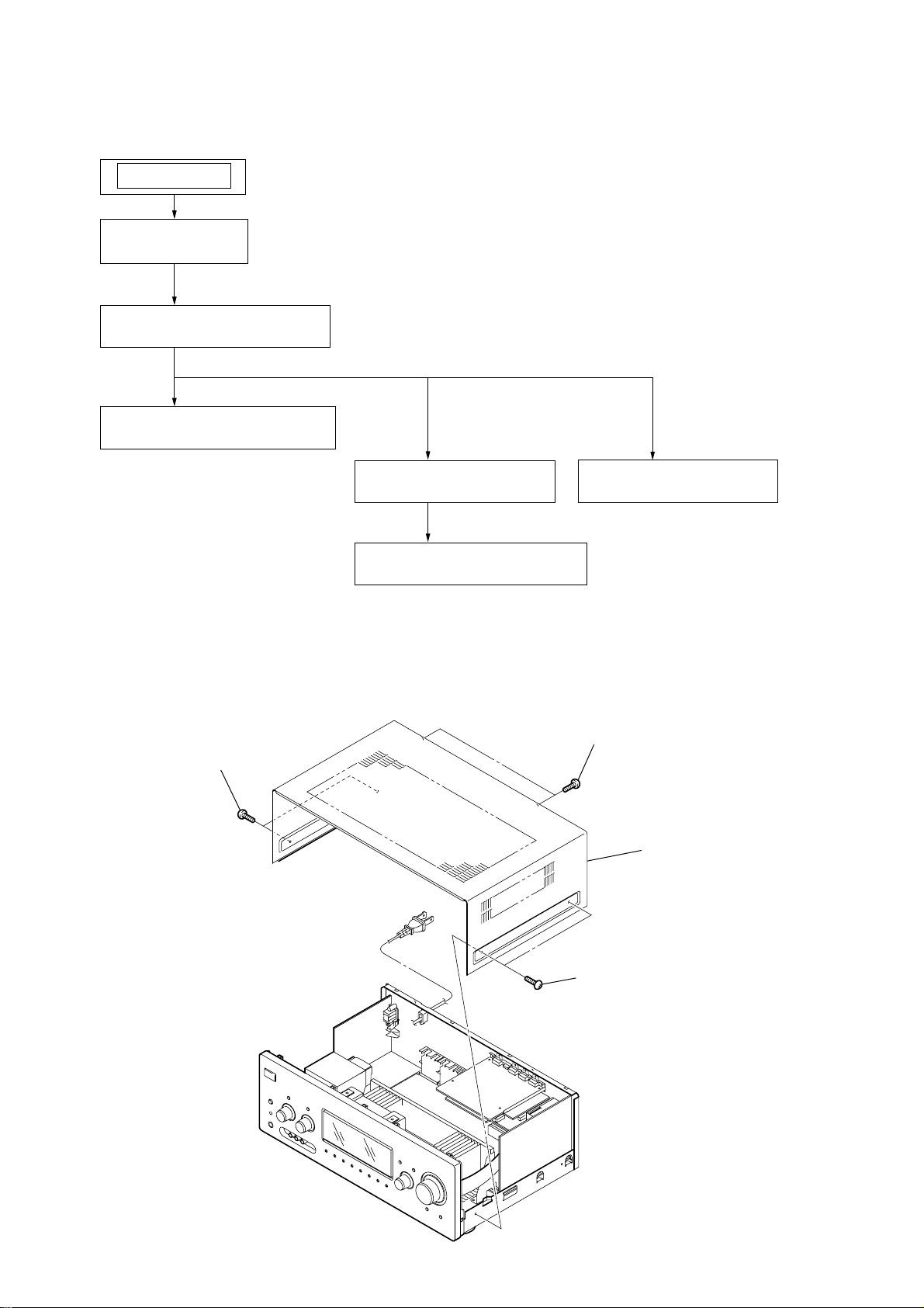
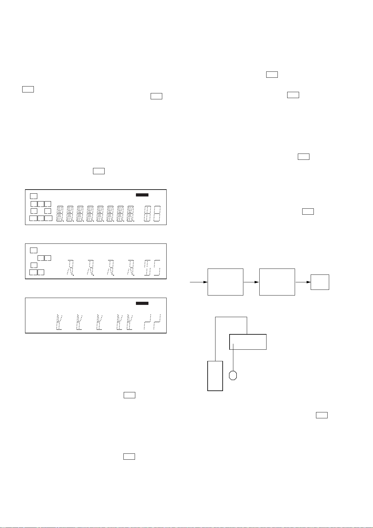
DISASSEMBLY
Note : This set can be disassemble according to the following sequence.
SET
2-1. CASE
(Page 8)
2-2. BACK PANEL SECTION
(Page 9)
2-3. FRONT PANEL SECTION
(Page 9)
2-4. DIGITAL BOARD
(Page 10)
2-5. MAIN BOARD SECTION
(Page 10)
Note : Follow the disassembly procedure in the numerical order given.
2-1. CASE
2
two
screws
(case 3 TP2)
2-6. STANDBY BOARD
(Page 11)
3
two
screws
(+BVTP 3
4
×
case
8
1
two
screws
(case 3 TP2)
8
2-2. BACK PANEL SECTION
)
)
2
CN3509 (5P)
CNP901 (2P)
1
8
three
(+BVTP 3
screws
×
qg
STR-DG810
9
screw
(+BVTP 3
8)
×
8)
0
three
(+BVTP 3
screws
×
8)
3
wire (flat type) (17 core)
(CN3511)
qa
two
screws
(+BVTP 3
qs
(+BVTP 3
×
8)
four
screws
×
8)
qd
three
screw
screws
(+BVTP 3
7
wire (flat type) (5 core
(CNS509)
qf
(+BVTP 3
×
×
8)
8)
qj
CNP203 (3P)
2-3. FRONT PANEL SECTION
5
two
(+BVTP 3
1
CNP790 (5P)
screws
×
6
wire (flat type) (9 core)
(CNS508)
ql
back panel section
5
wire (flat type) (9 core)
(CNS503)
4
CNP103 (3P)
qh
wire (flat type) (5 core)
qk
CNP202 (3P)
8)
(CN504)
3
CNP507 (3P)
4
CNP503 (3P
7
front panel section
2
wire (flat type) (27 core)
(CNS505)
6
five
screws
(+BVTP 3
×
8)
9
STR-DG810
n
2-4. DIGIT AL BOARD
3
CNP500 (7P)
2
CNP503 (8P)
1
CNP501 (3P)
5
DIGITAL board
4
screw
(+BVTP 3
×
8)
2-5. MAIN BOARD SECTION
5
(+BV3 (3
screw
6
(+BV3 (3
two
-CR)
screws
)
-CR)
4
CN915 (6P)
)
3
CNP912 (3P)
1
CNP801 (5P)
2
CNP802 (6P)
7
two
screws
(+BV3 (3
8
MAIN board sectio
-CR)
)
10
2-6. STANDBY BOARD
4
screw
(+BVTP 3
5
STANDBY board
×
STR-DG810
1
8)
3
CNP805 (3P)
CNP902 (2P)
2
CNP804 (3P)
11
STR-DG810
SPK Front Left
DCAC MIC
Receiver
SECTION 3
TEST MODE
AM CHANNEL STEP 9 kHz/10 kHz SELECTION
MODE
* Either the 9 kHz step or 10 kHz step can be selected for the AM
channel step.
* Procedure:
Turn the [INPUT SELECTOR] control to set AM and press the
?/1 button to turn off the main power.
While depressing the [TUNING MODE] button, press the ?/1
button to turn on the main power.
Either the message “9k STEP” or “10k STEP” appears for a
moment and select the desired step.
VACUUM FLUORESCENT DISPLAY TEST MODE
* All fluorescent segments are tested.
When this test is activated, all segments light on at the same
time, then each segment lights on one after another.
* Procedure:
While depressing the [TUNING MODE] and the [DISPLAY] buttons simultaneously, press the ?/1 button to turn on the main
power.
1. ALL segments light on.
SP A
SW
LFE
L
CR
SL S SR
SBL SB SBR
DDD
D
DEX DTS-ESxIIPL RDS STCAT96/24
SP B
D
D
PL OPT
MEMORY
NEO:6COAXHDMI
dB
MHz
MONOD.RANGESAT
Hzk
ft.m
KEY CHECK MODE
* Button check
* Procedure:
While depressing the [SPEAKERS $OFF/A/B/A+B%] and the [2CH]
buttons simultaneously, press the
?/1 button to turn on the
main power.
Either the message “REST 15” appears.
Every pressing of any button other than the
?/1 counts down
the buttons. The buttons which are already counted once are not
counted again. When all buttons are pressed “REST 00” appears.
SWAP ALL MODE
* The signal will be swap to all channel so that all speaker will
have sound output.
* Procedure:
1. While depressing the [SPEAKERS $OFF/A/B/A+B%] and the
[A.F.D.] buttons simultaneously, press the power ?/1 button to
turn on the main power.
2. “SWAP” appears. (No change while displayed.)
SHIPMENT MODE
All preset contents are reset to the default setting.
* Procedure:
1. While depressing the [SPEAKERS $OFF/A/B/A+B%] and the
[MUSIC] buttons simultaneously, press the power ?/1 button
to turn on the main power.
2. “CLEARED” appears and switch off the set.
2. Turn the [INPUT SELECTOR] control, confirm display.
LFE
L R
S
EX -ESx RDS
SP B
NEO:6COAXHDMI
k
m
MHz
MONOD.RANGESAT
3. Turn the [INPUT SELECTOR] control, confirm display.
LFE
SP A
SP B
D
D
EX -ESxIIPL STCAT96/24
OPT
NEO:6COAXHDMI
MEMORY
dB
Hz
ft.
MONOD.RANGESAT
4. Turn the [INPUT SELECTOR] control, all segments light off.
SOUND FIELD CLEAR MODE
* The preset sound field is cleared when this mode is activated.
Use this mode before returning the product to clients upon
completion of repair.
* Procedure:
While depressing the [2CH] button, press the ?/1 button to turn
on the main power.
The message “S.F. CLR.” a ppears for a moment and initialization is performed.
SOFTWARE VERSION DISPLAY MODE
* The software version is displayed.
* Procedure:
While depressing the [SPEAKERS $OFF/A/B/A+B%] and the
[DISPLAY] buttons simultaneously, press the ?/1 button to turn
on the main power.
The model name, destination and the software version are displayed for a moment.
DCAC FACTORY TEST MODE
DCAC Factory Test mode have two stages:
1. DCAC DSP Data Line Checking
2. DCAC board Checking
Start Pass Pass
DSP Data Line
Check
Factory Test System Setup
1. When power off:
Press the three buttons [MEMORY/ENTER] + [MOVIE] +
“DCAC[]FTM” appears.
Afterward, press the [TUNING MODE] to start DCAC factory
test mode.
Auto Cal Mic
Check
END
?/1 .
12

STR-DG810
SECTION 4
FM TUNER CHECK
1. DCAC DSP Data Line Checking
After press the [TUNING MODE], DCAC Factory test mode will start,
below display will show:
“DCAC[][][]x” x=1, 2, 3
If there is error happen, below display will show:
“ERR[]SD0x” x=1 t D1501 or R1530 problem
x=2 t D1502 problem
x=3 t D1503 problem
2. DCAC board Checking
Connect front left speaker of the receiver and AUTO CAL microphone. Turn [MASTER VOLUME] jog, there will be test tone sound
output from front left speaker, and the display will change accordingly.
“AD[]-[]xxx” xxx=0 to 255 (depends on loudness of test tone)
FM AUTO STOP CHECK
(1) Turn on the set.
(2) Input the following signal from Signal Generator to FM
antenna input directly.
* Carrier Frequency: A=87.5 MHz, B=98 MHz, C=108 MHz
Deviation : 75 kHz
Modulation : 1 kHz
ANT input : 35 dBu (EMF)
(Note)
Please use 75 ohm “coaxial cable” to connect SG and the set. You
cannot use video cable for checking.
Please use SG whose output impedance is 75 ohm.
(3) Set to FM tuner function and scan the input FM signal with
automatic scanning.
(4) Confirm that input Frequency of A, B and C are detected and
automatic scanning stops.
The stop of automatic scanning means “The station signal is
received in good condition.”
13
STR-DG810
d
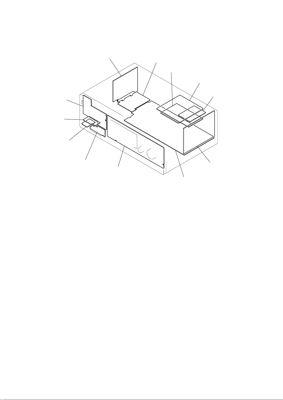
• Circuit Boards Location
SECTION 5
DIAGRAMS
POWER KEY board
DCAC board
HEADPHONE board
VIDEO 3 board
STANDBY board
DCDC board
VIDEO board
HDMI RE board
XM board
DIGITAL boar
DISPLAY board
MAIN board
14
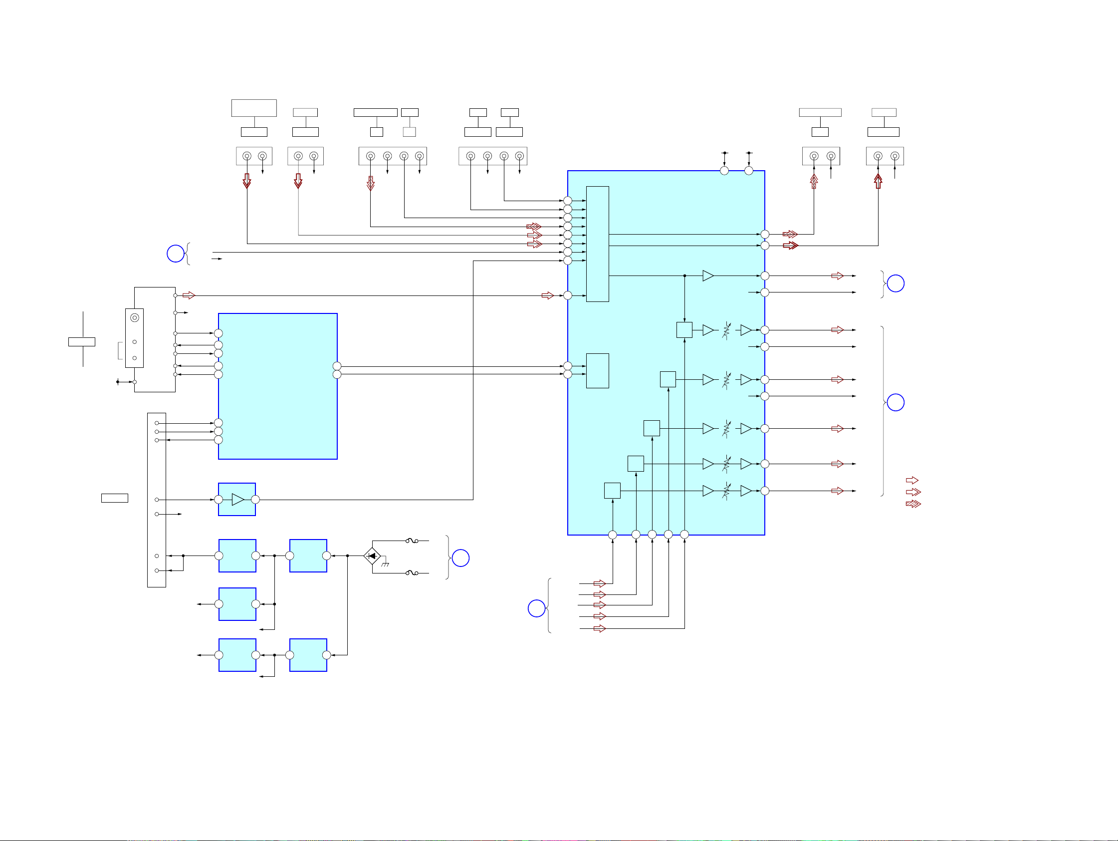
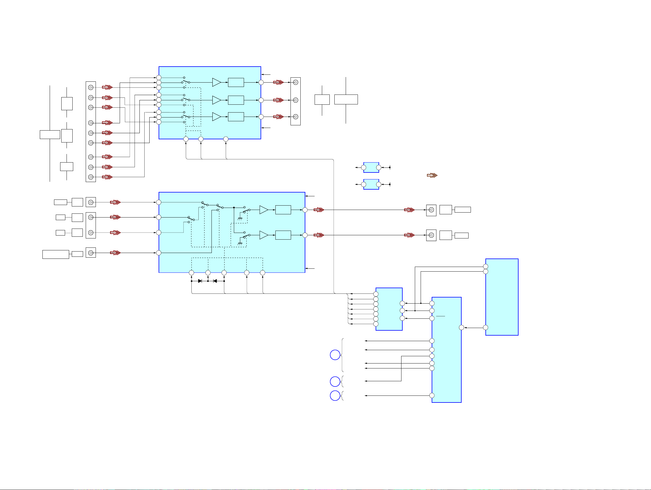
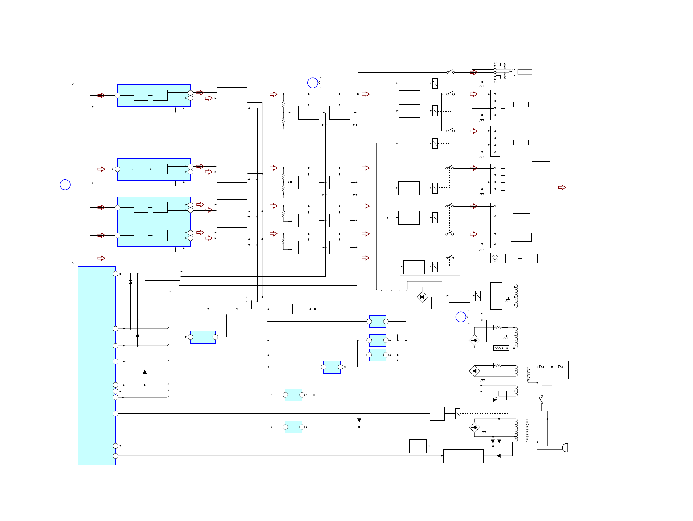
5-1. BLOCK DIAGRAM — TUNER/AUDIO SECTION —
VIDEO 3 IN/
PORTABLE AV IN
VIDEO 1
SA-CD/CD/CD-R
STR-DG810
TV
SAT
DVD
SA-CD/CD/CD-R
VIDEO 1
ANTENNA
FM 75Ω
COAXIAL
AM
TU+9V
(Page 19)
XM
SECTION
TN1
FM/AM TUNER UNIT
L-CH
R-CH
TUNED
CE
DO/ST
DI
CL
7
DET
5
RXD
6
TXD
AUDIO
LR
J298 (2/2) J405 (1/2)
XML
E
XMR
R-CH
R-CH
117
RDS SIGNAL
TUNLAT
27
26
TUNEDO
T_DI
22
T_CLK
13
101
CLINK_DET
100
CLINK_RX
CLINK_TX
99
R-CH
CONTROL
IC1010 (1/7)
-3 -4
SYSTEM
AUDIO IN
LR
R-CH
VOL DA
VOL CL
J402 (1/2)
11
10
IN IN
LRLR
-3 -4 -5 -6-2 -3
R-CH
R-CH
AUDIO IN
-1 -2 -3 -4
AUDIO IN
LRLR
R-CH
R-CH
J403
OUT
ANALOG SOUND
PROCESSOR
IC401
26
30
32
34
SEL
24
SW
28
22
36
38
L
SEL
60
MCU
I/F
59
SEL
SL
SEL
C
–7V
68 66
R-CH
R-CH
R-CH
+7V
J405 (2/2)
VCCVEE
46
44
41
42
88
87
85
84
86
LR
-1 -2
R-CH
AUDIO OUT
-1 -2
L-IN
R-IN
L-CH
R-CH
SL-CH
SR-CH
C-CH
LR
R-CH
A
C
J402 (2/2)
DIGITAL
SECTION
(Page 16)
POWER
SECTION
(Page 21)
J1302
DMPORT
VBUS
+5V
SW
SBL
SEL
SEL
BUFFER
IC3002
13
L
14
R
R–CH
3 1
81
SW-CH
• Signal path
: TUNER (FM/AM)
83
SBL-CH
: VIDEO (AUDIO)
: CD (ANALOG)
• R-ch is omitted due to
same as L-ch.
F4001
F4002
R2 AC
R2 AC
D
POWER
SECTION
(Page 21)
DIGITAL
SECTION
(Page 16)
SBLOUT
SW OUT
C OUT
B
SL OUT
L OUT
RECT
2
4
+5V
+3.3V
+5V REG
4 2
IC1012
+5V REG
3 1
IC1031
+6.3V
+3.3V REG
4 2
IC1013
+4.1V
+6.5V REG
2 1
IC4001
+4V REG
2 1
IC4100
D4001
54
56 51 52 49
STR-DG810
15 15
STR-DG810
5-2. BLOCK DIAGRAM — DIGITAL SECTION —
J2500
AUTO CAL MIC
DIGITAL
(ASSIGNABLE)
VIDEO
SECTION
(Page 17)
TUNER/
AUDIO
SECTION
(Page 15)
DVD
IN
(COAXIAL)
VIDEO1
IN
(OPTICAL)
SAT
IN
(OPTICAL)
DCAC_ON/OFF
TC74HC153_A
F
TC74HC153_B
HDMI SELECT
+3.3V(MIC)
A
BUFFER
Q2500
J1301
IC1352
IC1351
L-IN
R-IN R-CH
1
OUT
1
OUT
MIC AMP
IC2501
3
IC2502
+3.3V REG
1
6
IC1303
WAVE
SHAPER
SELECTOR
IC1302
6
5
4
AB
14 2
13
+5V
SELECTOR
5
1
23
7
IC1015
10
SWITCH
Q1007
12.288MHz
X1301
3
R-CH
5
3
21
22
1
2
DIGITAL AUDIO
I/F RECEIVER
IC1301
DIN2
INPUT
XOUT
XIN
+3.3V
31
VDD
ADC
IC1603
L IN
∆Σ
MOD.
R IN
DATA
DEMODULATOR
Pa,Pb DETECTION LOCK
C bit DETECTION
MICROPROCESSOR
I/F
CLKCEDI
38 37 36 35 46 17
45 46 47 48
HDMI
SECTION
(Page 18)
DIGITAL
DECIM.
FILTER
SCKI15BCK11LRCK
DO
SD0–SD3
LRCK
MUTE ERROR
HDMI SPDIF
12
7
CKSEL0
XSTATE
48
MCK
BCK
8
AUDIO
SD IN
CKOUT
DATAO
ERROR
XMODE
BCK
LRCK
DSP EX3
IC1009
DSPIC
80
I
I
DSPIE
SD0
CLOCK SELECTOR
IC1008
2
3
5
6
10
11
13
14
24
13
14
15
16
2
34
1
ERROR DETECT
D1301
IC1017
4 79
7 88
9
12 89
1
6
5
CLOCK
GENERATOR
IC1016
82
78
DPSIA
DPSIB
DPLRCK
DPBCK
97
NON AUDIO
1
8
DIR_ERR
16
15
INT_REQ
122
SPIDS
121
RESET
SPICLK
1256127
BUFFER
IC1004
5 2
3
MOSI
DPDVBCK
DPDVLRCK
63
1
7
DPSOA
CLKIN
XTAL
DPSOB
DPSOC
DPFSCK
DPSOD
FLAG3
SPI_MAS
126
142
143
MISO
64
65
70
94
71
87
86
98
7
X1302
25MHz
IC1014
SWITCH
5 1
SPI SELECT
IC1003
2
1
47
45
46
31
38
40
41
S.FLASH
IC1011
SO
2
SI
5
6
SCK
CE
1
5
DATA3
DATA1
DATA2
DATA4
SCKI
BCK
LRCK
8CH DAC
IC1452
MDO
MDI
34
DAC
DAC
DAC
DAC
35
MC
AMP
IC1403
VOUT5
10
VOUT6
9
VOUT1
14
VOUT2
13
VOUT3
VOUT4
11
VOUT7
16
VOUT8
20
ML
RST
3633
37
3
R-CH
5
R-CH
312
5
5
AMP
IC1405
AMP
IC1404
AMP
IC1406
1
L OUT
7
SL OUT
TUNER/
B
AUDIO
SECTION
1
C OUT
7
SW OUT
7
SBL OUT
(Page 15)
• Signal path
: TUNER (FM/AM)
: VIDEO (AUDIO)
: DVD (DIGITAL)
G
DOUT
PDWN
10
20
XMCK
DETECTION
• R-ch is omitted due to
383
39
63
64
65
83
49
50
91 90 6689
67
128
2
72
69
same as L-ch.
STR-DG810
ANALOG SW DATA
DIR CLK
DIR CE
DIR DI
DIR DO
DIR CKST
DIR XSTATE
DIR XMODE
DIR DATAO
DSP SPIDS
DSP RESET
SYSTEM
CONTROL
IC1010 (2/7)
1616
DSP INT
DIR ERROR
HDMI_FSRATE
SPI CLK
DSP MOSI
DSP MISO
SF_DSP_MAS
SF_CPU_CE
DACDO
DAC ATC
DAC DI/XMDACMDI
DAC CLK/XMDACMC
AD/DA RST
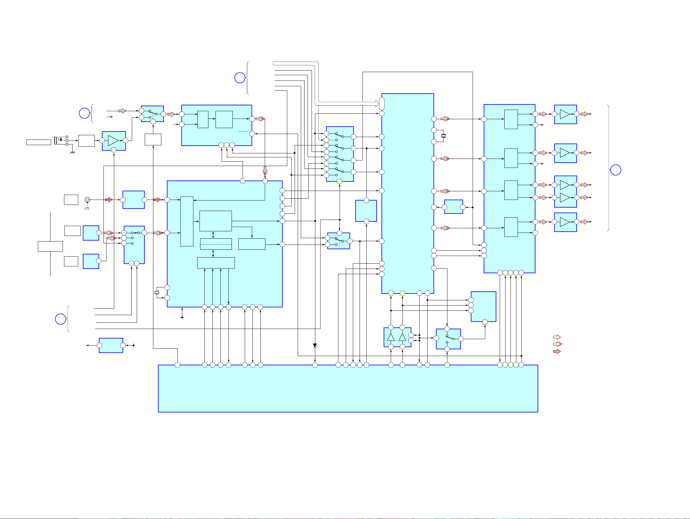
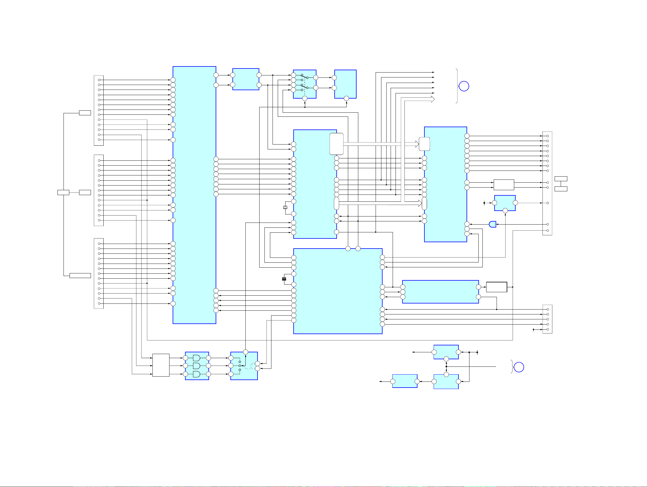
5-3. BLOCK DIAGRAM — VIDEO SECTION —
1
3
5
7
9
11
16
14
12
13
5
3
9
COMPONENT
VIDEO
VIDEO 1
VIDEO 3 IN/
PORTABLE AV IN
VIDEO 1
DVD
SAT
SAT
VIDEO
IN
DVD
VIDEO
IN
IN
P
PR/CR
P
PR/CR
P
PR/CR
–1
VIDEO
IN
–2
VIDEO
IN
–1
VIDEO
IN
–1
VIDEO
Y
B/CB
Y
B/CB
Y
B/CB
J301
–1
–2
–3
–4
V5
–6
V7
–8
–9
J201 (1/2)
J200 (1/2)
J298 (1/2)
COMPONENT VIDEO SELECT
IC304
CH1 IN1
CH1 IN2
CH1 IN3
CH2 IN1
CH2 IN2
CH2 IN3
CH3 IN1
CH3 IN2
CH3 IN3
SW1 SW2
2 4
COMP_S1 COMP_S2
INPUT
SELECTOR
IC203
V1
DVD
SAT
V3
6dB AMP
6dB AMP
6dB AMP
P.SAVE
21
75Ω
DRIVER
75Ω
DRIVER
75Ω
DRIVER
V MUTE
CH1 OUT
CH2 OUT
CH3 OUT
V+1,+2
22
20
18
V-1,-2
6dB AMP
6dB AMP
+5V-3
–5V-3
75Ω
DRIVER
75Ω
DRIVER
J302
–1
–2
–3
M.OUT
V1 OUT
Y
PB/CB
R/CR
P
1
15
VCC
MONITOR
OUT
+5V-3
COMPONENT
VIDEO
+5V-3
–5V-3
IC807
+5V
2 1
REG
IC804
–5V
2 1
REG
+15V
–15V
• Signal path
: VIDEO
J201 (2/2)
J200 (2/2)
-2
VIDEO
OUT
-3
VIDEO
OUT
MONITOR
VIDEO 1
SYSTEM CONTROL
IC1010 (3/7)
STR-DG810
SW1
14
D203 D204
V_SW1
SW5
2
SW2
10 4
V_SW2
SW3
V_SW3
SW4
6
V_SW4
VEE
–5V-3
DIGITAL
SECTION
(Page 16)
(Page 21)
POWER
SECTION
HDMI
SECTION
(Page 18)
F
H
I
V MUTE
COMP_S2
COMP_S1
V_SW4
V_SW3
V_SW2
V_SW1
HDMI SELECT
DCAC_ON/OFF
TC74HC153_A
TC74HC153_B
HP RY
REG CTRL
VIDEO CONTROL
IC230
15
QA
2
QC
QD
3
4
QE
QF
5
QG
6
7
QH
CLK
LAT
S-IN
D595LAT
35
33
D595CLK
VIDEO CONTROL
BUFFER
IC1602
11
12
14
11
CLK
12
LAT
9
S-OUT
14
S-IN
15
QA
1
QB
2
QC
5
QF
6
QG
7
QH
32
D595DATA
STR-DG810
17 17
STR-DG810
5-4. BLOCK DIAGRAM — HDMI SW SECTION —
HDMI
CN3501
SAT IN
CN3502
DVD IN
CN3503
VIDEO 2/BD IN
1
DATA2+
3
DATA2–
DATA1+
4
DATA1–
6
7
DATA0+
DATA0–
9
CLOCK+
10
CLOCK–
12
13
CEC
15
SCL(5V)
SDA(5V)
16
18
+5V POWER
HOT PLUG DET
19
1
DATA2+
3
DATA2–
4
DATA1+
6
DATA1–
7
DATA0+
9
DATA0–
10
CLOCK+
12
CLOCK–
13
CEC
15
SCL(5V)
16
SDA(5V)
18
+5V POWER
19
HOT PLUG DET
1
DATA2+
3
DATA2–
4
DATA1+
6
DATA1–
7
DATA0+
9
DATA0–
10
CLOCK+
12
CLOCK–
13
CEC
15
SCL(5V)
SDA(5V)
16
18
+5V POWER
19
HOT PLUG DET
SWITCHER
IC3503
39
58
A34
57
B34
55
A33
54
B33
52
A32
51
B32
49
A31
48
B31
46
SCL3
45
SDA3
44
HPD3
A24
77
B24
76
A23
74
B23
73
A22
71
B22
70
A21
68
B21
67
SCL2
64
SDA2
63
62
HPD2
15
A14
14
B14
12
A13
11
B13
9
A12
8
B12
6
A11
5
B11
3
SCL1
2
SDA1
80
HPD1
SDA_SINK
SCL_SINK
HPD_SINK
XOE
38
34
Y1
35
Z1
31
Y2
32
Z2
28
Y3
29
Z3
25
Y4
26
Z4
40
21
S1
22
S2
23
S3
42
DATA BUFFER
IC3507
3
SDAA6SDAB
2
SCLA SCLB
7
X3501
28.322MHz
X3502
10MHz
EEPROM DATA SELECT
IC3521
5
1
14
12
41
DSDA
42
DSDL
51
RXC+
50
RXC–
55
RXO+
54
RXO–
59
RX1+
58
RX1–
63
RX2+
62
RX2–
84 XTALOUT
85 XTALIN
44
PWR5V
91
INT
89
RESET
19
RX_RST
20
RX_INT
35
EEPROMSEL1
XOUT
11
XIN
13
21
RX_HPDI
51
TMDS_S1
52
TMDS_S2
53
TMDS_S3
54
TMDS_OEB
55
P5V_SELA
56
P5V_SELB
3
13
10 7
HDMI RX
IC3511
92-96
99-105
QE23
108-111
I
114-117
QE0
121-124
VSYNC
HSYNC
DE
SPDIF
WS
SCK
MCLK
SD3
I
SD0
CSDA
CSCL
MUTE
HDMI CONTROL
EEPROM
5
SDA
6
SCL
119,
1
128
127
70
75
76
79
71
I
74
39
40
67
IC3519
IC3509
WP
28 27
CSCLCSDA
TX_5VPWR
TX_RST
TX_INT
MUTE
RESET
232_OUT
232_IN
CNVSS
MUTE ERROR
SPDIF
LRCK
BCK
MCL
SD0–SD3
HDMI TX
IC3513
D23
49-58
I
61-70
75-79
D0
2
VSYNC
1
HSYNC
80
DE
5
SPDIF
11
WS
12
SCK
6
MCLK
SD3
7
I
I
SD0
10
44
CSDA
43
CSCL
41
42
43
65
33
TX
34
RX
10
29
30
7
30
HDMI_ERR
102
FLASH_SO/HDMI_UART_TX
103
FLASH_SO/HDMI_UART_RX
SYSTEM CONTROL
IC1010 (4/7)
G
36
TX2+
35
TX2–
33
TX1+
32
TX1–
30
TX0+
29
TX0–
TXC+
27
26
TXC–
20
DSCL
19
DSDA
18
HPD
17
INT
42
RESET
CEC OUT
HDMI RESET
DIGITAL
SECTION
(Page 16)
+6.3V
IC3501 (2/2)
29
104
DATA BUFER
5 4
11 12
CEC BUFFER
Q1103–1106
Q3504
POWER
CONTROL
IC3516
1
SDA(5V)
+5V POWER
HOT PLUG DET
HDMI+3.3V
DATA2+
DATA2–
DATA1+
DATA1–
DATA0+
DATA0–
CLOCK+
CLOCK–
SCL(5V)
CEC
10
12
15
16
18
19
13
CN3510
1
3
4
6
7
9
2
RESET
3
232_OUT
5
232_IN
1
CNVSS
3.3V
7
CN3504
HDMI
OUT
STR-DG810
+5V REG
Q305–307
POWER DETECT
IC3501 (1/2)
1
5
9
3
6
8 5
3
2
4
B
9
10
A
POWER SELECT
IC3504
HDMI+1.8V
HDMI+3.3V
+1.8V REG
3 1
IC3528
+3.3V REG
4 2
IC3526
1
1
+3.3V REG
4 2
IC3527
+4.1V
REG CTRL
I
VIDEO
SECTION
(Page 17)
1818
5-5. BLOCK DIAGRAM — XM SECTION —
XM AUDIO
DIGITAL PROCESSOR
IC102
3
SCTXOUT
5
SCRXIN
18 COMRXP
19 COMRXT
+D
2
J101
XM
–D
3
23 COMTXP
22 COMTXM
92
XM MIXMO
93
XM MIXMI
SYSTEM CONTROL
IC1010 (5/7)
STR-DG810
X101
45.158MHz
26 OSCOUT
28 OSCIN
I2SSCLK
I2SDATA
I2SLRCLK
I2SOCLK
RESET
D/A CONVERTER
IC105
13
MD
14
VOUTL
VOUTR
MC
ML
15
AUDIO AMP
IC104
7
8
6 7
2
XML
1
XMR
TUNER/AUDIO
E
SECTION
BCK
39
37
41
43
1
2
DATA
3
LRCK
SCK
16
72
DAC DI/XMDACMDI
2
DAC CLK/XMDACMC
7
XM DAC MS
(Page 15)
11
IC106
XM+5.3
4 2
V REG
IC107
XM+5V
3 1
REG
+6.3V
XM+5.3V
XM+5V
XM+3.3V
POWER CONTROL
SWITCH
Q105,106
IC101
XM+3.3V
3 1
REG
97
XMRESET
84
RDSCLK/XMDPOWER
STR-DG810
19 19
STR-DG810
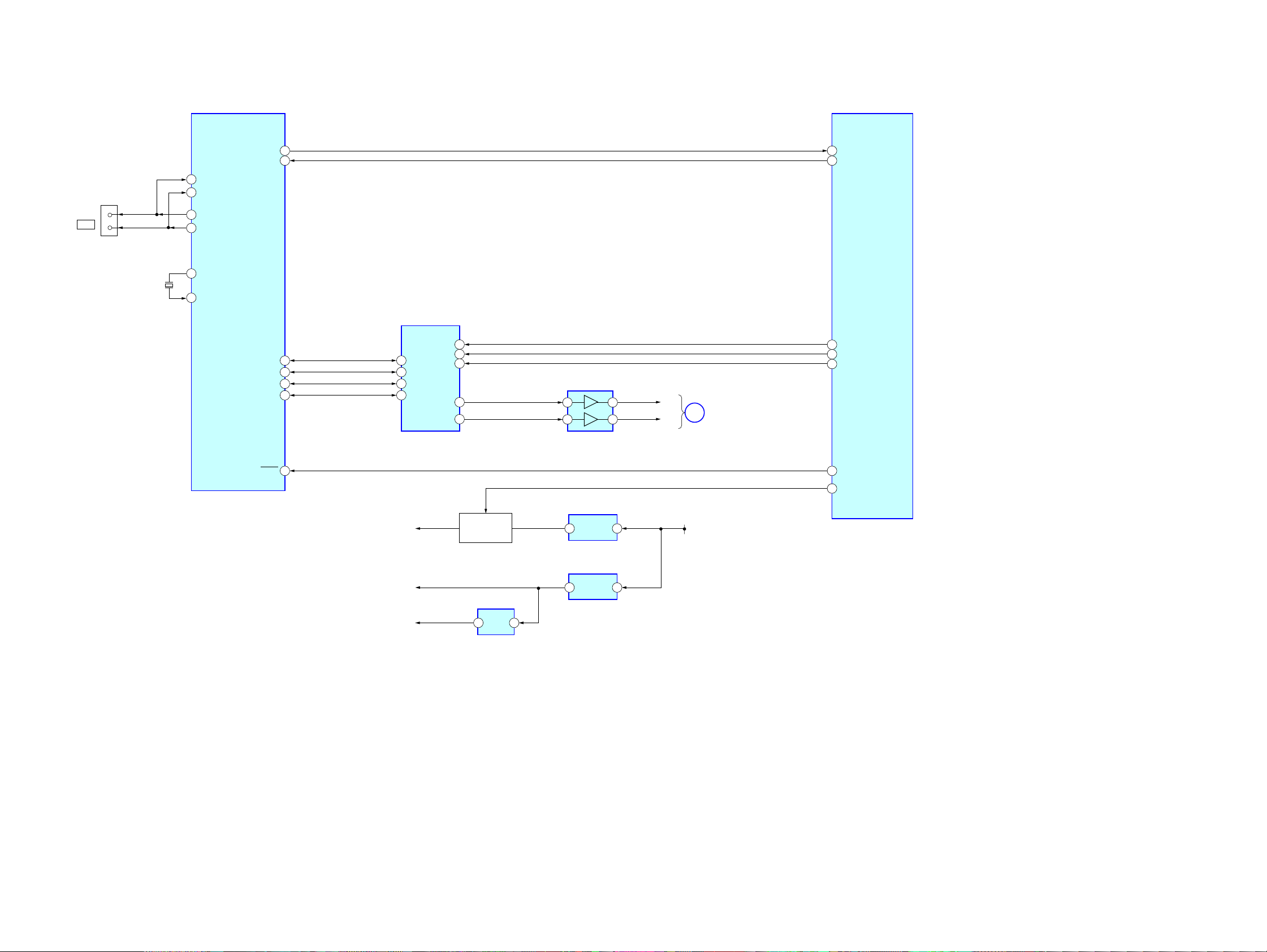
5-6. BLOCK DIAGRAM — KEY/DISPLAY SECTION —
FLASH
PROGRAMMING
CNS504
9
8
1
2
7
5
EEPROM
IC1131
SDA
SCL
SDA
SCL
FLASH-SO
FLASH-SI
MD2
XRESET
SIRCS
FL DISPLAY DRIVER
IC100
STB
9
DIN
7
CLK
8
OUT
2
2
3
2
3
SEG1
I
SEG17
GRID1
I
GRID11
REMOTE
CONTROL
SIGNAL
RECEIVER
IC103
RV102
MASTER
VOLUME
RV101
INPUT
SELECTOR
14
I
29
•
31
42
I
32
FL101
VACUUM
FLUORESCENT
DISPLAY
F1
F2
SYSTEM
CONTROL
IC1010 (6/7)
BUFFER
IC101
68
FL_LAT
71
57
X1300
12.5MHz
5
6
12.5MHz
12.5MHz
58
EEPROM DATA
98
EEPROM CLK
78
V_ENCODER(A)-DOWN
103
FLASH_SO/HDMI_UART_TX
102
FLASH_SI/HDMI_UART_RX
MD2
52
FL_DATA
FL_CLK
SIRCS IN
V_ENCODER(B)-UP
INPUT ENCODER A
INPUT ENCODER B
70
82
16
15
79
80
9
4
2
8
6
3
RESET
IC1005–1007
S100
I
/
I
55
INIT
62
RESET
85
POWERKEY
TUNING ENCODER+/- A
TUNING ENCODER+/- B
TONE JOG A
TONE JOG B
A/D KEY1
A/D KEY2
36
37
6
5
114
115
SW NETWORK
S101-108
2
3
2
3
SW NETWORK
S109–115
RV103
– TUNING +
RV104
– TONE +
STR-DG810
2020
5-7. BLOCK DIAGRAM — POWER SECTION —
STR-DG810
TUNER/
AUDIO
SECTION
(Page 15)
C
L-CH
R-CH
SL-CH
SR-CH R-CH
C-CH
SBL-CH
SW-CH
PROTECTOR
SYSTEM
CONTROL
IC1010 (7/7)
BRIDGEABLE RY
R-CH
FRONT_RY
C/SB RY
SW_RY
SP_BRY
HP DETECT
POWER_RY
STOP
SUB T
R-CH
PRE DRIVER
IC701
+VOUT2
IN 2
PRE
8
8
8
6
61
17
21
23
20
8
25
9
81
94
IN 2
IN 2
IN 1
D1110
DRIVE
DRIVE
DRIVE
DRIVE
D1107
D1111
DRIVE
PRE DRIVER
IC601
PRE
DRIVE
PRE DRIVER
IC501
PRE
DRIVE
PRE
DRIVE
PROTECTOR
D721,722,732,733
Q722,723,725,793,795
FRONT A RY
C/SB/REAR RY
SW RY
FRONT B RY
HP DETECT
BRIDGEABLE RY
-VOUT2
-45V +B
+VOUT2
-VOUT2
-45V +B
+VOUT2
-VOUT2
+VOUT1
-VOUT1
-45V +B
12
11
12
11
12
11
2
3
IC691
OVERLOAD
DETECT AMP
–45V
B-SWITCH
Q691,692
72
POWER AMP
Q701-704
POWER AMP
Q651-654
POWER AMP
Q501-504
POWER AMP
Q533,534
571,572
+B
-B
TU+9V
-20V
+7V
-7V
+A5V
+1.2V
+3.3V
(STBY)
VIDEO SECTION
(Page 17)
R-CH
R-CH
-20V REG
Q801
IC1002
+1.2V
REG
IC1904
+3.3V
REG
HP RY
H
CURRENT
DETECT
Q705,706
R-CH
CURRENT
DETECT
Q655,656
R-CH R-CH
CURRENT
DETECT
Q505,506
CURRENT
DETECT
Q535,536
IC1001
+3.3V
13
13
OVERLOAD
DETECT
D740,Q740
OVERLOAD
DETECT
D640,Q640
OVERLOAD
DETECT
D540,Q540
OVERLOAD
DETECT
D580,Q580
+5V
REG
R-CH
13
D1001
FRINT B RY
IC1902
+9V
REG
IC801
+7V
REG
-7V
REG
IC802
FRONT A RY
13
31
23
SW RY
C/SB/REAR RY
HP DETECT
+15V
-15V
RELAY
DRIVER
Q790
RELAY
DRIVER
Q710
RELAY
DRIVER
Q611
RELAY
DRIVER
Q610
RELAY
DRIVER
Q612
RELAY
DRIVER
RECT
D802
Q560
RY791
RY701
RY710
RY601
RY610
BRIDGEABLE RY
AC IN
DETECT
Q921
RY560
TUNER/
SECTION
(Page 15)
RELAY
DRIVER
Q901
RELAY
DRIVER
Q809
AUDIO
D920-923
D805-808
RY901
D910-913
SUB TRANSFORMER
VOLTAGE CONTROL
R-CH
R-CH
R-CH
D
RECT
RECT
RECT
Q922,923
R2 AC
R2 AC
-20V
RY801
F1
F2
TB001 (1/2)
TB001 (2/2)
D914
TM602
TM603
J309
RELAY
SW
D804
D924
R810
R811
R910
D915
PHONES
L
FRONT A
R
L
FRONT B
R
L
SURROUND
R
CENTER
SURROUND
BACK
AUDIO
OUT
POWER
TRANSFORMER
(MAIN)
POWER
TRANSFORMER
(SUB)
J790
WOOFER
T901
T903
SPEAKERS
IMPEDANCE
USE 8-16Ω
SUB
• Signal path
: TUNER (FM/AM)
• R-ch is omitted due to
same as L-ch.
F901 F902
AC IN
J911
AC OUTLET
~
STR-DG810
21 21
STR-DG810
THIS NOTE IS COMMON FOR PRINTED WIRING BOARDS AND SCHEMATIC DIAGRAMS.
(In addition to this, the necessary note is printed in each block.)
for schematic diagram:
• All capacitors are in µF unless otherwise noted. (p: pF)
50 WV or less are not indicated except for electrolytics
and tantalums.
• All resistors are in Ω and 1/
specified.
f
•
• 2 : nonflammable resistor.
• 5 : fusible resistor.
• C : panel designation.
Note: The components identified by mark 0 or dotted line
• A : B+ Line.
• B : B– Line.
•Voltage and waveforms are dc with respect to ground
•Voltages are taken with a VOM (Input impedance 10 MΩ).
•Waveforms are taken with a oscilloscope.
• Circled numbers refer to waveforms.
• Signal path.
: internal component.
with mark 0 are critical for safety.
Replace only with part number specified.
under no-signal (detuned) conditions.
no mark : FM
Voltage variations may be noted due to normal production tolerances.
Voltage variations may be noted due to normal production tolerances.
F : TUNER (FM/AM)
L : VIDEO (AUDIO)
I : VIDEO
J : DVD (DIGITAL)
c : CD (ANALOG)
4
W or less unless otherwise
for printed wiring boards:
• X : parts extracted from the component side.
f
•
• : Pattern from the side which enables seeing.
Caution:
Pattern face side: Parts on the pattern face side seen from the
(Side B) pattern face are indicated.
Parts face side: Parts on the parts face side seen from the
(Side A) parts face are indicated.
: internal component.
C
Q
B
E
Q
BCE
Q
B
C
E
These are omitted.
These are omitted.
• Waveforms
— DIGITAL Board —
1
IC1301 qd (CKOUT)
12.288 MHz
1 V/DIV, 50 nsec/DIV
2
IC1301 qf (BCK)
3.07 MHz
1 V/DIV, 0.2 µsec/DIV
3
IC1301 wa (XOUT)
12.288 MHz
3.5 Vp-p
3.5 Vp-p
3.1 Vp-p
— HDMI RE Board —
1
IC3511 if (XTALOUT)
28.322 MHz
1 V/DIV, 20 nsec/DIV
2
IC3519 qa (XOUT)
10 MHz
1 V/DIV, 50 nsec/DIV
— XM Board —
1
IC102 wh (OSCOUT)
2.2 Vp-p
3.4 Vp-p
1 V/DIV, 50 nsec/DIV
4
IC1009 <zcv (XTAL)
25 MHz
0.5 V/DIV, 20 nsec/DIV
5
IC1010 tj (12.5MHz)
12.5 MHz
1 V/DIV, 50 nsec/DIV
1.2 Vp-p
3.2 Vp-p
45.158 MHz
1 V/DIV, 50 nsec/DIV
0.8 Vp-p
STR-DG810
2222
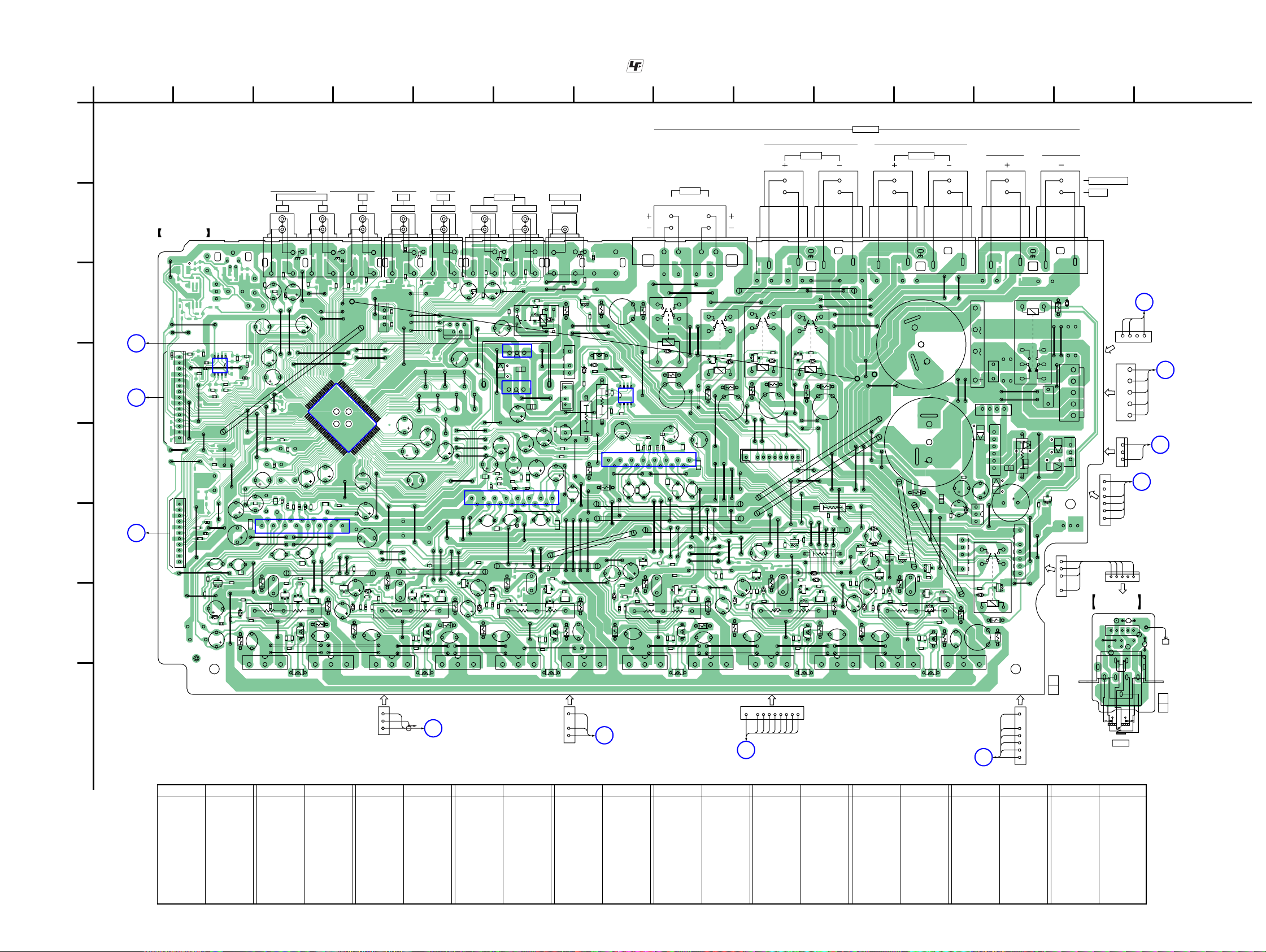
5-8. PRINTED WIRING BOARDS — MAIN SECTION — • Refer to page 14 for Circuit Boards Location. : Uses unleaded solder.
STR-DG810
A
B
C
D
E
F
G
H
XM
BOARD
CN102
(Page 39)
DIGITAL
BOARD
CNS501
(Page 27)
DIGITAL
BOARD
CNS502
(Page 27)
1
234567891011 12 13 14
MAIN BOARD
JW506
JW521
C3037
JW522
CNP501
JW309
CN500
JW367
11
1
R3022
15
R3023
C3026
4
IC3002
C3025
R3013
R3012
JW524
C3027
JW518
1
JW486
R423
C468
R429
JW312
C469
R428
JW440
C565
JW485
Q580
BE
R586
JW469
R585
C580
D580
C581
TP800
G
A
B
• Semiconductor Location
Ref. No. Location Ref. No. Location Ref. No. Location Ref. No. Location
D505 G-4
D540 G-4
D560 C-6
D580 G-2
D585 G-2
D605 G-10
D610 D-9
D611 D-10
D640 G-7
D665 G-7
JW338
C570
R3010
R3011
SPEAKERS
IMPEDANCE USE 8-16Ω
FRONT A
JW390
R767
JW411
R737
C761
R766
JW310
R763
GRY
BLU
JW459
Q722
BE
JW328
GRY
RY610
BE
Q612
R635
JW424
JW360
10
JW476
JW378
R780
JW408
R773
BE
BE
R760
R761
Q752
10
CNP914
GRY
L
R
JW413
JW366
R633
D611
R518
L501
JWH306
JWH311
JW374
JW435
JW482
R792
JW339
D722
D721
R775
Q755
C770
R769
Q756
EB
Q751
JW533
JW549 JW550
EB
TM602
J405
SA-CD/CD/CD-R
OUT
-1
L
R409
R459
R472
C459
R471
JW526
JW525
C3024
R3021
1
R3020
JW523
85
JW443
JW325
C554
R554
R587
JW346
R534
R574
C702
C3032
C762
C3022
JW505
JW431
JW438
R475
R476
JW415
C464
C495
R553
R561
JW373
C553
C741
2
R741
1
C732
JW341
JW410
C504
JW471
R537
R588
C531
R580
D585
R526
R572
JW379
C577
R576
Q533 Q534
Q536
BE
JWH305
C566
R523
R571
IN
-3
L
-2
R
R452
C409
JW460
JW552
C3034
JW527
50
51
C488
C490
R503
C567
R562
C507
C506
R502
IC501
JW319
JW386
C505
R505
JW423
JWH309
R535
C539
JW302
BE
R530
Q535
R531
EB
R570
Q571
C576
JW542
JW543
EB
Q572
JW420
JW555
JW528
C485
TV
IN
-5
L
-4
R
R402
31
R501
14
R555
R575
JW308
IC401
80
15
JW445
Q540
BE
30
JW347
C510
WP100
JW465
JW541
JW544
-6
R
R454
R404
VIO
CNP503
3
JW500
1
JW529
JW530
1
100
81
C561
JW363
C503
C733
R556
C540
D505
R546
R524
R522
C541
R557
D540
R514
C517
3
1
CNP503
SAT DVD
AUDIO IN
-1
L
C403
R405
R455
C453
C463
JW503
C493
C481
JW368
JW324
JW457
R517
Q506
C511
BE
R540
R516
JW364
R513
Q503
PNK
BLK
WHT
J403
AUDIO IN
-3
L
-2
R
R457
JW395
JW353
JW315
JW464
JW515
JW514
JW511
C492
C501
JW455
JW340
R573
JWH319
R525
R520
BE
Q505
EB
R510
R511
Q501
JW545 JW546
BE
Q502
F
-4
R
R458
R407
CN504
1
4
2
C808
JW517
JW516
JW512
JW510
C484
JW306
JW419
JW307
JW318
JW416
JW458
Q740
C519
R521
R515
C516
Q504
VIDEO 3
BOARD
CN201
(Page 33)
JW392
JW453
JW323
JW468
BE
AUDIO OUT
R474
C458
5
JW508
R703
15
JW352
R745
C710
JW539JW540
R746
-1
L
JW388
J402
VIDEO 1
AUDIO IN
-3
L
-2
R
C444
R406
R456
R408
C408
JW406
R473
C703
C705
C740
D740
R714
RY560
R468
C471
123
IC801
D896
IC802
321
JW375
C807
JW358
C701
C751
R751
R701
R702
R752
C707
C757
C706
IC701
JW314
C704
JL001
R704
JW331
D705
R717
R724
R748
R740
R722
C742
R747
C717
Q703 Q704
J309
SUB WOOFER
AUDIO OUT
-4
R
C400
JW332
R469
JW553
R710
Q702
D560
R601
R651
1
JWH308
BE
BE
Q705
EB
R699
C744
R725
Q706
EB
JW538
Q611
R470
E
B
R738
R802
R632
JW335
JW442
1
Q692
EB
CN505
D691
4
D690
R696
R698
1
CN506
4
R691
JW397
R692
B
Q691
E
JW448
JW441
R733
JW330
R732
C755
JW477
JW470
JW361
R744
JW344
JW362
JWH313
JW454
JW393
JW407
C720
R719
R721
R715
C716
Q701
1
4
CN505
JW537
RED
GRY
GRY
E
L751
JW320
R690
8
IC691
R695
1
C691
R693
R694
C653
15
14
JW474
JW452
JW409
C660
R677
D640
R648
C642
R664
VIDEO
BOARD
CNP203
(Page 33)
R768
JW428
5
4
C657
R653
IC601
R654
C655
C654
BE
Q640
C640
R667
D665
R674
R640
R672
C666
Q653
R532
R533
BE
Q560
JW396
C810
JW336
C811
C601
C651
C753
R753
C756
214
R754
C754
JW437
JW377
JW354
R723
C711
R716
R711
JW447
R713
Ref. No. Location
D680 G-10
D690 D-7
D691 D-7
D701 D-8
D705 G-5
D710 D-8
D721 F-10
D722 F-10
D732 F-10
D733 F-10
D740 G-5
D750 G-9
D765 G-9
D791 G-12
D801 F-11
D802 D-12
D804 E-12
D805 E-13
D806 E-12
D807 E-12
D808 E-13
D818 C-13
D896 D-6
IC401 D-4
IC501 F-3
IC601 E-7
IC691 D-7
IC701 E-6
IC801 D-6
IC802 D-6
IC3002 D-2
Q501 G-5
Q502 H-5
Q503 H-4
Q504 H-5
Q505 G-5
Q506 G-4
Q533 H-3
FRONT B
LR
JW483
JW382
RY710
JW451
D701
R718
L701
JW532
R602
C603
C743
R675
C661
JW433
JW383
R666
R663
C607
JW425
R603
C606
1
2
R604
C605
C604
JWH304
JW351
JWH310
JW405
JW414
JW479
R676
R673
BE
Q655
R669
BE
Q656
EB
R660
R661
Q651
JW536
JW547
EB
Q652
C656
R652
JW462
JW399
JW356
R638
C670
JW402
RY701
R731
Q710
BE
D710
R668
R734
L651
JW355
R743
JW473
JW417
JW327
JW391
JW446
JW475
JW337
JW426
JW311
JW484
JW436
JW372
R755
R756
JW463
C760
R671
R665
R764
C669
JW535
JW548
Q654
JWH312
RY601
R631
Q610
BE
D610
R618
R634
L601
JW418
JW434
JW357
CNP914
1
JW359
JW478
JWH301
R736
JW449
C722
Q750
BE
D765
C750
R778
R758
R757
R750
R772
D750
C752
C766
Q753
1
BLU
GRY
GRY
GRY
GRY
C
DIGITAL BOARD
CNP503
Ref. No. Location Ref. No. Location
Q534 H-3
Q535 G-3
Q536 G-3
Q540 G-4
Q560 C-6
Q571 G-3
Q572 H-3
Q580 F-2
Q601 G-11
Q602 H-11
(Page 27)
Q603 H-11
Q604 H-11
Q605 G-11
Q606 G-11
Q610 D-9
Q611 C-7
Q612 D-9
Q640 F-7
Q651 G-8
Q652 H-8
TB001
JW376
JW400
JW429
JW412
JW305
VIO
WP102
WP101
JW350
JW380
JW334
JW371
JW467
R794
JW365
JW450
JW317
Q795
JW534
JW342
D732
C791
EB
R770
C721
BE
Q680
C680
R655
R656
C610
C681
D680
R614
R735
JW370
R765
JW472
R771
C767
Q754
Ref. No. Location Ref. No. Location
Q653 H-7
Q654 H-8
Q655 G-8
Q656 G-8
Q680 F-10
Q691 E-6
Q692 D-7
Q701 G-6
Q702 H-6
Q703 H-6
SURROUND
L
R
C804
JW348
C803
JW389
R803
JWH317
D733
Q723
Q725
BE
BE
JW369
R623
R617
C611
D605
R624
R680
R681
R657
R622
R616
Q605
R611
JW422
C621
R613
Q603 Q604
JW321
BE
R790
BE
Q606
BE
R625
R610
EB
EB
Q602
JW343
C809
R804
JW398
JWH315
Q793
C619
R620
Q601
R615
BCEBCEBCEBCEBCEBCEBCEBCEBCEBCEBCEBCE
STANDBY
BOARD
CNP802
(Page 44)
JW322
D802
C805
JW349
JW551
CNP507
4
1
CNP802
1
D804
D807
C830
6
R806
D806
C801
C822
C832
EB
C802
Q801
D801
CN792
C620
JW381
5
RY791
1
Q790
R791
BE
D791
R621
R793
L551
R568
RED
GRY
GRY
GRY
GRY
GRY
I
Q704 H-7
Q705 G-6
Q706 G-6
Q710 D-8
Q722 F-9
Q723 F-11
Q725 F-10
Q740 G-5
Q750 F-9
Q751 G-9
TM603
RY801
JW404
JW556
R910
CN915
1
7
JW329
1-872-424-
1
7
CN915
D818
R830
JW385
JW519
CNP801
5
JW394
C806
1
CNP912
3
D805
JW507
1
C831
D808
Q809
BE
R824
JW403
JW531
CN792
GRY
5
GRY
GRY
RED
1
11
(11)
Ref. No. Location
Q752 H-9
Q753 H-9
Q754 H-10
Q755 G-9
Q756 G-9
Q790 G-12
Q793 F-11
Q795 F-10
Q801 F-12
Q809 E-12
SURROUND BACK
CENTER
CNP912
BLU
1
GRY
RED
YEL
GRN
6
CNP802
GRY
GRY
HEADPHONE
BOARD
CL073
5
CNP790
JW791
CL074
J790
PHONES
(Page 42)
DISPLAY
BOARD
CN108
GRY
GRY
CNP801
5
1
GRY
3
ORG
1
GRY
RED
15
C791
1
CL072
H
RED
CNP507
14
RED
BLU
BLK
YEL
ORG
K
TRANSFORMER
CNP790
TP790
CL071
C790
1-872-433-
J
TRANSFORMER
(Page 44)
DIGITAL
BOARD
D
CNP500
(Page 27)
T901
POWER
(MAIN)
(Page 44)
BLK
(CHASSIS)
12
(12)
T901
POWER
(MAIN)
STR-DG810
23 23
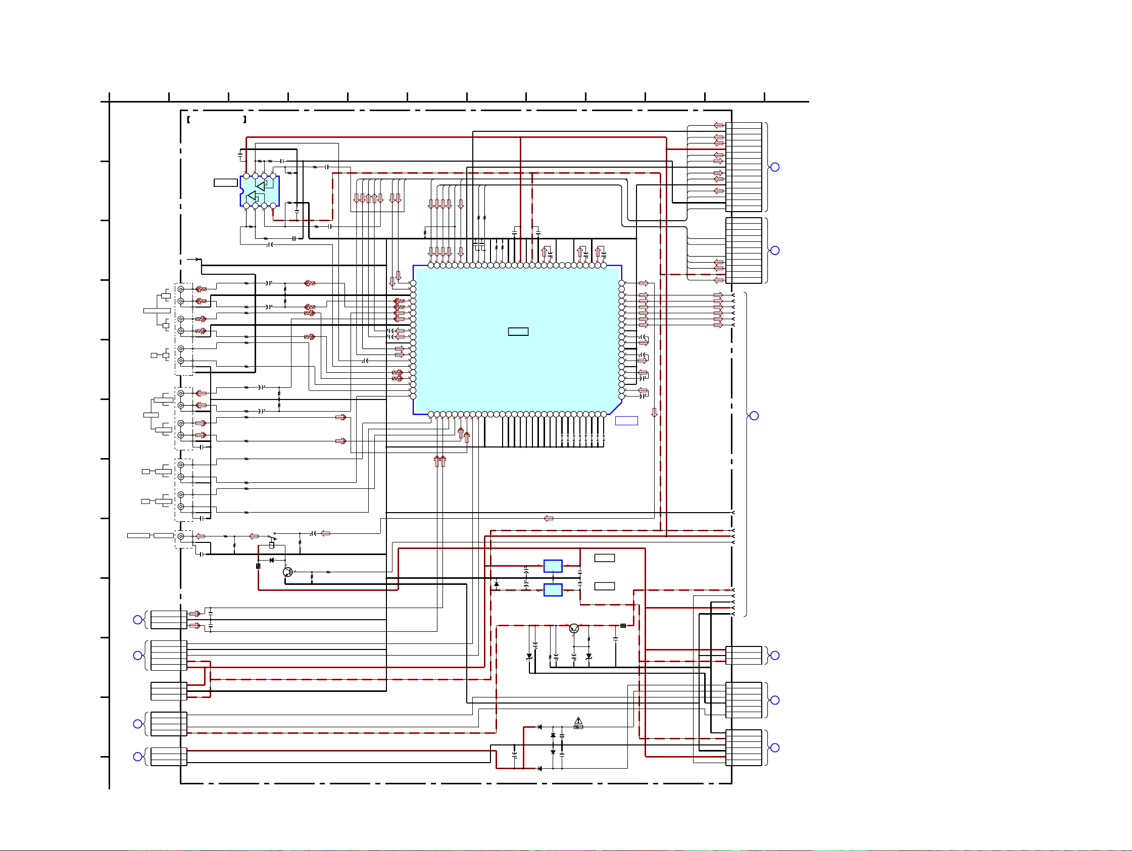
STR-DG810
5-9. SCHEMATIC DIAGRAM — MAIN SECTION (1/2) — • Refer to page 46 for IC Block Diagrams.
A
B
C
D
E
F
G
H
I
(Page 34)
(Page 40)
J
K
(Page 43)
(Page 31)
L
VIDEO 3
BOARD
CN201
XM
BOARD
CN102
DISPLAY
BOARD
CN108
DIGITAL
BOARD
(4/5)
CNP500
SUB WOOFER
F
G
H
D
SA-CD/CD/CD-R
TV
AUDIO OUT
VIDEO 1
AUDIO IN
SAT
AUDIO IN
DVD
AUDIO IN
AUDIO OUT
J405
6P
OUT
IN
IN
J402
4P
J403
4P
J309
1P
+7V (R4)
GND (R4)
L
R
L
R
L
R
L
R
L
R
L
R
L
R
L-CH
GND
R-CH
XMR
GND
XML
-7V
+7V
+7V
GND
-7V
-20V
2
MAIN BOARD
WP100
-1
-2
-3
-4
-5
-6
G
-1
-2
-3
-4
G
C444
2200p
-1
-2
-3
-4
G
C403
2200p
G
C400
2200p
CNP503
3P
1
2
3
CN504
5P
1
2
3
4
5
CN506
3P
1
3
4
CNP507
4P
1
F1
2
NC
3
F2
4
CNP912
3P
1
2
NC
3
IC3002
IC3002
NJM4565M(TE2)
BUFFER
R469
1k
220p
C463
220p
C453
(1/2)
0.1C3025
700
8765
VCC
-+
000
R3020
47k
R409
1k
R459
1k
R402
1k
R452
1k
R404
1k
R454
1k
R408
1k
R458
1k
R406
1k
R456
1k
R405
1k
R455
1k
R407
1k
R457
1k
47k
R470
R802
220
R3010
R3011
47k
47k
+
R3021
0.5%
47k
C409
C459
C408
50V4.7
C458
50V4.7
RY560
D560
1SS355WTE-17
CN500
11P
CNP501
15P
CN505
3P
CNP802
6P
CN915
6P
11
1
C OUT
2
MAIN AGND
3
SW OUT
4
L OUT
5
+7V
6
R OUT
7
R IN
8
GND
9
L IN
10
T.R OUT
11
GND
12
T.L OUT
13
C LINK_R
14
AGND
15
C LINK_L
1
V3_R
2
V3_L
3
V3_GND
4
VOL IC_CLK
5
VOL IC_DATA_LAT
6
VACS CTRL
7
SBR_OUT
8
SBL_OUT
9
SR_OUT
10
-7V
11
SL_OUT
A3
A4
A5
A6
A7
A8
A9
A10
A11
A12
A13
A14
A15
A16
A17
1
+15V
3
GND
4
-15V
6
+R4
5
-R4
4
F2
3
GND
2
NC
1
F1
1
R2 RETURN GND
3
-15V
4
STBY GND
5
R2 GND
6
+15V
7
SUB-T
A
B
MAIN
BOARD
1
(2/2)
(Page 25)
E
K
I
1241
DIGITAL
BOARD
(2/5)
CNS501
(Page 29)
DIGITAL
BOARD
(5/5)
CNS502
(Page 32)
VIDEO
BOARD
CNP203
(Page 34)
T901
POWER
TRANSFORMER
(MAIN)
(Page 44)
STANDBY
BOARD
CNP802
(Page 44)
579
C3022
1
0.5%
0
VEE
4321
-7
50V4.7C3034
50V4.7
50V4.7
47k
R473
47k
R474
R3013
47k
R3023
47k
0.1
C3026
C3032
1
47k
R471
47k
R472
R468
100k
2SC3052EF-T1-LEF
0.1
47k
C471
50V
Q560
RELAY DRIVER
0.7
47k
R533
R3012
47k
0.5%
R3022
4.7
C3027
1
L-IN
R-IN
TU-L
TU-R
C3037
1
0.5%
R532
10k
L-OUT
R-OUT
LINK-L
LINK-R
C762
50V10
C702
50V10
50V4.7C3024
6
C-OUT
SL-OUT
SR-OUT
SW-OUT
VOL-CLK
SBL-OUT
SBR-OUT
VOL-DATA
1kR429
1kR428
100pC469
100pC468
10kR475
000
CLK
DGND
INAL
INAR
DATA
PORTA
AGND8
BOUT2
AGND3
1SR154-400TE-25
10kR476
C488
0.1
0
PORTB
AGND9
ANALOG SOUND
PROCESSOR
BOUT1
AGND2
D896
D804
PTZ-TE25-5.6B
D805-808
RECT
C832
3300
16V
IC401
BD3451KS
INBSW
R423
0
0
00000
51 52 53 54 55 56 57 58 59 60 61 62 63 64 65 66 67 68 69 70 71 72 73 74 75 76 77 78 79 80
INCC
INCSL
INCSB
INCSB
INCSR
INCSW
INDR
AGND7
INBL
INBR
INCL
INCR
INDL
0
INCR
50
0
INCL
49
AGND6
48
0
ROUTBR
47
0
ROUTBL
46
0
ROUTAR
45
0
ROUTAL
44
AGND5
43
0
AOUTR
42
0
AOUTL
41
AGND4
40
0
INIR
39
0
INIL
38
0
INHR
37
0
INHL
36
0
INGR
35
0
INGL
34
0
INFR
33
0
INFL
32
0
INER
31
INEL
000000000
AGND10
IC401
INBSBR
7
VCC
INBSBL
C464
0.1
-700
VEE
AGND11
AGND12
INBC
INBSL
INBSR
7
C807
47
25V
C808
47
25V
-7
C822
47
35V
R806
22k
D808
1SR154-400TE-25
D805
1SR154-400TE-25
D806
1SR154-400TE-25
D807
1SR154-400TE-25
C495
50V10
GOUTSW
INBR
IC801
TA7807S
IC802
TA79007S
8
VINSW
INBL
G
2
1
G
AGND13
AGND1
VINSBR
GOUTSBR
INASBR
INASW
JW516
JW517
JW508
31
16.5
IO
IO
23
-17.3
Q801
2SB734-T-34
-20V REG
-22
-22.3
C801
47
35V
C831
0.47
C830
0.47
C490
000
AGND14
GOUTSBL
INASR
INASBL
JW515
-47.2
C802
47
35V
R910
0.15
1/2W
50V10
JW512
C811
0.47
C810
0.47
VINSBL
INASL
JW514
C485
50V10
0
VINSR
AGND15
GOUTSR
OUTSW
OUTSBR
OUTSBL
OUTSR
OUTSL
AGND16
GOUTL
AGND17
GOUTR
AGND18
GOUTC
AGND19
GOUTSL
INAL
INAR
INAC
123456789101112131415161718192021222324252627282930
JW510
JW511
IC801
+7V REG
IC802
-7V REG
C809
R804
0.1
10k
100V
D801
UDZSTE-1722B
OUTC
OUTR
OUTL
VINR
VINSL
VINL
VINC
0
81
82
0
83
0
84
0
85
0
86
0
87
0
88
89
0
90
0
91
92
0
93
0
94
95
0
96
0
97
98
0
99
0
100
IC B/D
R803
4.7
C484
C481
C492
C493
50V10
103
C-OUT
SW-OUT
L-OUT
R-OUT
R-IN
L-IN
TU-R
TU-L
LINK-R
LINK-L
VOL-CLK
VOL-DATA
SBR-OUT
SBL-OUT
SR-OUT
SL-OUT
50V10
50V10
50V10
STR-DG810
2424
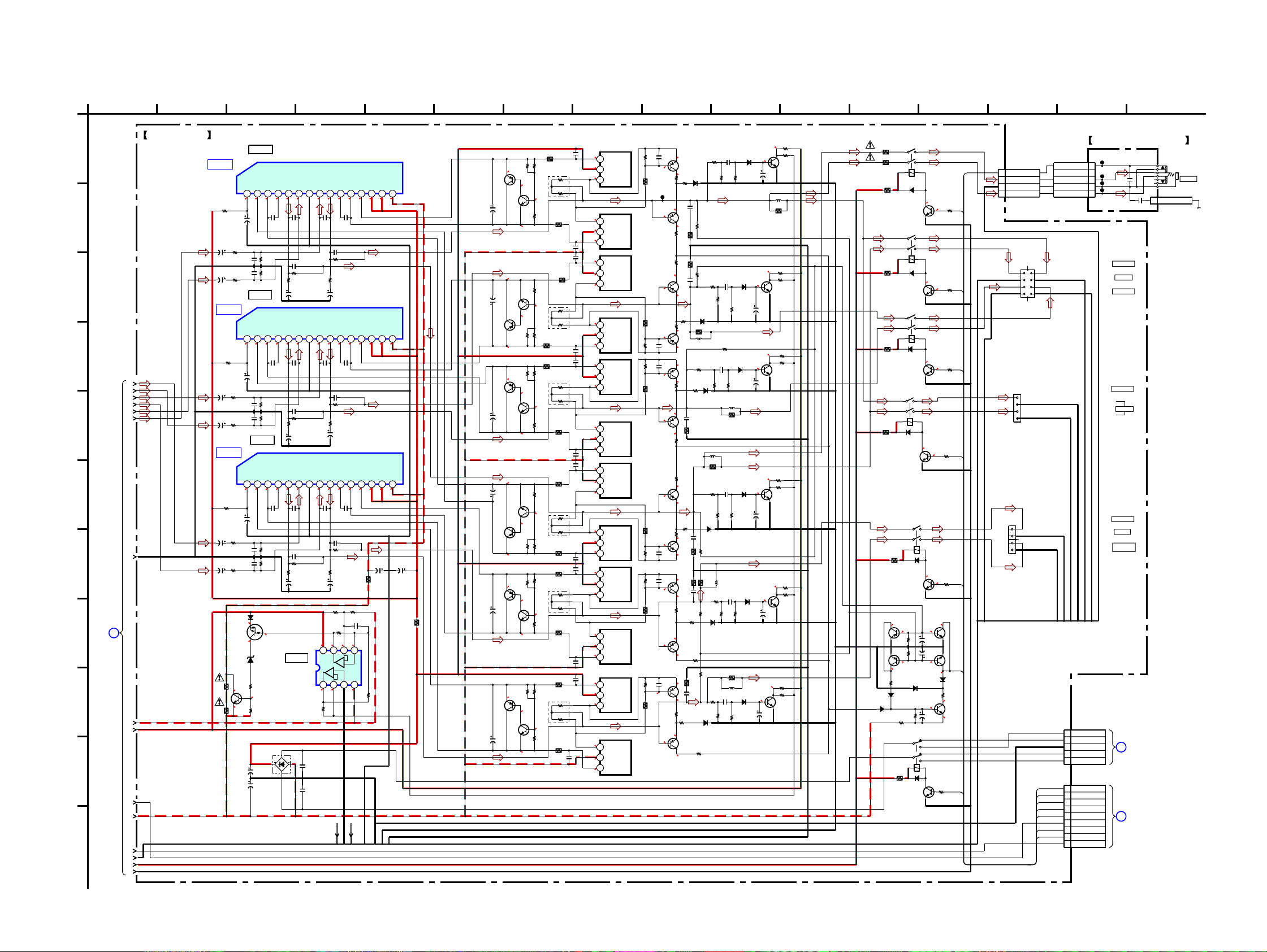
5-10. SCHEMATIC DIAGRAM — MAIN SECTION (2/2) — • Refer to page 46 for IC Block Diagrams.
STR-DG810
A
B
C
D
E
F
G
H
I
J
K
MAIN
BOARD
(1/2)
(Page
24)
3
MAIN BOARD (2/2)
IC701
IC B/D
A3
A4
A5
A6
A7
A8
A9
1
R691
R692
A10
A11
A12
A13
A14
A15
A16
A17
PRE DRIVER
+VOUT1
-VOUT1
MUTE
198765432 151413121110
2.9
1.1
R744
22k
2%
C701
50V4.7
C751
50V4.7
IC B/D
R743
22k
2%
C651
50V4.7
C601
50V4.7
IC B/D
R741
22k
2%
C561
50V4.7
C501
50V4.7
100
2W
330
2W
R651
R601
R561
R501
R701
R751
1k
1k
1k
-1.1
100V2.2
C744
C755
R702
C707
68k
1k
100p
R752
C757
68k
100p
1k
IC601
PRE DRIVER
+VOUT1
-VOUT1
MUTE
198765432 151413121110
1.1
2.9
-1.1
C605
2.2
C743
100V
R652
C657
68k
100p
C607
R602
100p
1k
IC501
PRE DRIVER
+VOUT1
-VOUT1
MUTE
198765432 151413121110
1.1
2.9
-1.1
C565
2.2
C741
100V
C567
68k
100p
R562
C507
68k
100p
R502
D691
1SS355WTE-17
6.5
Q692
DTA124ESA-TP
B- SWITCH
-5.6
6.4
D690
UDZSTE-1730B
R698
10k
-47.2
-46.7
Q691
2SC1815GR-TPE2
B- SWITCH
R699
-47.4
470k
D802
D5SBA20-4003
RECT
C803
0.01F
71V
C804
0.01F
71V
NF1
COMP1
0
-45.3
C756
100p
500V33p
NF1
COMP1
0
-45.3
C606
500V33p
100p
R603
NF1
COMP1
0
-45.3
C566
100p
500V33p
IC691
NJM4565M(TE2)
OVERLOAD
DETECT AMP
R753
2.2k
2%
C753
10V
2.2k
2%
C603
10V
R553
2.2k
2%
C553
IC691
0
100
0
100
0
µPC2581V-S
IN1
µPC2581V-S
IN1
µPC2581V-S
IN1
10V100
C805
0.22
100V
C806
0.22
100V
4
IC701
GND
IN2
0
0
C706
100p
500V3pC754
2%68kR754
IC601
GND
IN2
0
0
C656
100p
500V3pC604
2%68kR604
IC501
GND
IN2
0
0
C506
100p
500V3pC554
2%68kR554
7
8765
VCC
+-
-5.6
R694
10k
NF2
COMP2
-45.5
C705
33p
500V
R703
2.2k
2%
C703
100
10V
NF2
COMP2
-45.5
C655
33p
500V
R65368k
2.2k
2%
C653
100
10V
NF2
COMP2
-45.5
C505
33p
500V
R503
2.2k
2%
C503
10V100
R696 R695
47k
R690
220k
-5.6
-4.5
+
1.2
-1.1
-1.1
-1.1
-VOUT2
500V3pC704
2%68kR704
-VOUT2
500V3pC654
-VOUT2
500V3pC504
2%68kR505
-5.6
4321
-7
WP101WP102
VEE
R693
0.1
TP790
C791 0.1
Ω
Ω
Ω
T901
POWER
TRANSFORMER
(MAIN)
(Page 44)
DIGITAL
BOARD
(5/5)
CNP503
16
1
LEAD TO CHASSIS
J790
PHONES
5P
9P
156
HEADPHONE BOARD
CNP790
5P
CL071
1
HP_DETECT
2
NC
CL072
3
R-CH
CL073
4
GND
CL074
5
L-CH
SPEAKERS
IMPEDANCE USE 8-16
+
FRONT A
+
SURROUND
-
SPEAKERS
IMPEDANCE USE 8-16
+
L
+
R
-
SPEAKERS
IMPEDANCE USE 8-16
+
CENTER
+
SURROUND
-
5
R1 (SIDE1)
4
R2 (SIDE2)
3
GND
2
R2 (SIDE2)
1
R1 (SIDE1)
1
PROTECTOR
3
FRONT A RY
4
C/SB/REAR_RY
5
HP_CTRL
6
HP_RY
7
WOOFER_RY
8
FRONT_B_RY
9
BRIDGEABLE_RY
10
SUB_T
C790
TB001
TM602
FRONT B
TM603
BACK
J
C
(Page 32)
9821
Q703
MN2488-OPY-MK
Q704
MP1620-OPY-MK
Q654
MP1620-OPY-MK
Q653
MN2488-OPY-MK
Q603
MN2488-OPY-MK
Q604
MP1620-OPY-MK
Q754
MP1620-OPY-MK
Q753
MN2488-OPY-MK
Q503
MN2488-OPY-MK
Q504
MP1620-OPY-MK
Q533
MN2488-OPY-MK
Q534
MP1620-OPY-MK
Q505,506,535,536,605,606,
Q655,656,705,706,755,756
CURRENT DETECT
R719
C720
4.7k
220p
2%
0
R722
R721
1.5k
6.2k
JL001
0
0
Q706
2SA1163L-TE85L
R725
68k
R638
68k
-36.8
Q655
2SA1163L-TE85L
0
R671
R672
6.2k
1.5k
Q656
2SA1163L-TE85L
0
R669
4.7k
C670
2%
220p
C619
R620
220p
4.7k
2%
Q605
0
2SA1163L-TE85L
R622
R621
1.5k
6.2k
0
0
Q606
2SA1163L-TE85L
-36.8
R625
68k
R775
68k
Q755
2SA1163L-TE85L
0
R771
R772
6.2k
1.5k
Q756
2SA1163L-TE85L
0
R769
C770
4.7k
220p
2%
R520
C519
4.7k
220p
2%
0
Q505
2SA1163L-TE85L
R521
R522
1.5k
0
0
Q506
2SA1163L-TE85L
R530
C539
4.7k
220p
2%
Q535
0
2SA1163L-TE85L
R531
6.2k
0
0
Q536
2SA1163L-TE85L
0
Q705
2SA1163L-TE85L
0
15kR724
D705
1SS355WTE-17
C711
0.022
-36.8
R717
10
R667
10
C661
0.022
0
R674
15k
1SS355WTE-17
0
L651
0
R680
0
R624
0
15k
1SS355WTE-17
C611
0.022
R617
10
-36.8
0
R778
15k
C761
0
0.022
R767
10
0
0
R517
10
C511
0.022
0
R5736.2k
47k
R524
15k
R525
68k
-36.8
R523
47k
R537
0
10
C531
0.022
0
R572
1.5k
R534
15k
1SS355WTE-17
-36.8
R535
R723
47k
R673
47k
R648
D665
4.7R668
22k
R681
15k
D605
R758
D765
1SS355WTE-17
R773
47k
R518
4.7
1SS355WTE-17
R588
D585
68k
Q501-504,533,534,571,572,
Q601-604,651-654,701-704,751-754
POWER AMP
C717
33R714
500V
47p
1.1
123
R710
R711
2.2k
82k
1.1
+VOUT2
VCC
VCC
VEE
1.1
46.9
46.9
-46.7
+VOUT2
VCC
VCC
VEE
1.1
46.9
46.9
-46.7
2%68kR654
+VOUT2
VCC
VCC
VEE
1.1
46.9
46.9
-46.7
C732
C733
100V10
100V10
1R733
10k
0.1C691
10k
R732
1
Q701
2SA1115TP-EF
C710
47
25V
C660
47
25V
Q651
2SA1115TP-EF
Q601
2SA1115TP-EF
C610
47
25V
C760
47
25V
Q751
2SA1115TP-EF
Q501
2SA1115TP-EF
C510
47
25V
Q571
2SA1115TP-EF
C570
47
25V
Q702
-1.1
Q652
1.1
1.1
Q602
-1.1
Q752
1.1
1.1
Q502
1.1
Q572
R660
R610
2SC3623ATP-LK
2SC3623ATP-LK
2.2k
2.2k
2SC3623ATP-LK
2SC3623ATP-LK
R760
2.2k
R510
2.2k
2SC3623ATP-LK
R570
2.2k
2%
2SC3623ATP-LK
R716 0.22X2 5W
0.5
-0.6
R713
R715
560
33
-1.1
C716
500V47p
C669
500V47p
R665
33
R663
560
-0.6
0.5
R666 0.22X2 5W
R661
82k
C666
R664
33
500V
47p
C621
33R614
500V
47p
R611
82k
R616 0.22X2 5W
0.5
-0.6
R613
560
-1.1
R615
33
C620
500V47p
C767
500V47p
R765
R763
33
560
-0.6
0.5
R766 0.22X2 5W
R761
82k
33R764
C766
500V
47p
C517
47p
500V
R511
33R514
82k
R516
R513
R571
-0.6
560
82k
-0.6
R576
560
0.22X2 5W
R515
33
C516
500V47p
C577
500V
47p
R574
33
R526 0.22X2 5W
33R575
C576
500V47p
0.5
-1.1
0.5
-1.1
47
0
0
-47.4
-1.1
-1.1
-47.4
0
0
47
1.1
1.1
47
0
0
-47.4
-1.1
-1.1
-47.4
0
0
47
1.1
1.1
47
0
0
-47.4
-1.1
1.1
47
0
0
-47.4
-1.1
B
C
E
E
C
123
B
123
B
C
E
E
C
123
B
123
B
C
E
E
C
123
B
123
B
C
E
E
C
123
B
123
B
C
E
E
C
123
B
123
B
C
E
E
C
123
B
R748
R640
15k
L751
R768
R750
15k
D505
R580
R740
22k
4.7
22k
R546
22k
15k
22k
15k
R540
15k
R623
C681
0.01
L501
22k
C742
0.01
R747
15k
2SC3052EF-T1-LEF
C642
0.01
1SS355WTE-17
R677
15k
47k
2SC3052EF-T1-LEF
1SS355WTE-17
R657
15k
L601
R618
4.7
C752
2SC3052EF-T1-LEF
0.01
1SS355WTE-17
R757
15k
C541
0.01
R557
15k
4.7R568
L551
C581
0.01
1SS355WTE-17
R587
10 135
Q540,580,640,680,740,750
OVERLOAD DETECT
Q740
2SC3052EF-T1-LEF
D740
1SS355WTE-17
Q640
0
D640
C640
10
50V
Q680
0
D680
C680
Q750
0
D750
C750
Q540
2SC3052EF-T1-LEF
D540
1SS355WTE-17
Q580
2SC3052EF-T1-LEF
0
D580
15k
1211
4.7kR745
6.5
R746
0
47k
C740
10
50V
L701
R718
4.7
4.7kR675
6.5
R676
47k
4.7kR655
6.5
R656
47k
10
50V
R755
4.7k
6.5
R756
47k
10
50V
R555
4.7k
6.5
R556
0
47k
C540
10
50V
R585
4.7k
6.5
1SS355WTE-17
1SS355WTE-17
C580
50V
R586
47k
10
R793
82
2SC3052EF-T1-LEF
R734
82
2SC3052EF-T1-LEF
R634
82
2SC3052EF-T1-LEF
R738
82
2SC3052EF-T1-LEF
RELAY DRIVER
2SC3052EF-T1-LEF
2SA1163L-TE85L
D722
D721
2SC3052EF-T1-LEF
RY791
1W680R792
1W680R794
D791
1SS355WTE-17
Q790
RELAY DRIVER
RY701
D710
1SS355WTE-17
Q710
RELAY DRIVER
RY601
D610
1SS355WTE-17
Q610
RELAY DRIVER
RY710
D701
1SS355WTE-17
Q611
R635
82
1SS355WTE-17
Q612
RELAY DRIVER
Q795
-40
0
R790
100k
R770
100k
0
2SC3052EF-T1-LEF
-40
Q725
2SA1163L-TE85L
R780
1SS355WTE-17
10k
2SC3052EF-T1-LEF
R7371kR736
39k
R830
82
1SS355WTE-17
Q809
RELAY DRIVER
RY610
D611
Q723
D732
Q722
RY801
D818
0.2
R791
0.8
0.2
R731
2.2k
0.7
0.2
R631
0.7
0
0
R632
2.2k
0.2
0.7
R633
1k
Q793
2SC3052EF-T1-LEF
3.3
0
C791
220
10V
C721
220
10V
0
3.3
R735
6.8k
3.2
-40.7
C722
10
50V
-46.5
R824
2.2k
2.2k
62
66
1k
68
64
68
61
D733
1SS355WTE-17
69
55
Q722,723,725,793,795
CN792
4P
PROTECTOR
1
3
4
5
+
-
+
-
HP_DETECT
R-CH
GND
L-CH
R(+)
R(-)
SR(+)
SR(-)
TM602
L(-)
R(-)
TM603
4P
147
TB001
8P
REDBLK BLKRED
L(+)
L(-)
SL(+)
SL(-)
4P
L(+)
R(+)
CNP801
CNP914
61
66
68
55
62
64
69
STR-DG810
25 25
 Loading...