

Sony STR-DE885, STR-DE985 Service Manual
STR-DE885/DE985
SERVICE MANUAL
Ver 1.0 2002. 05
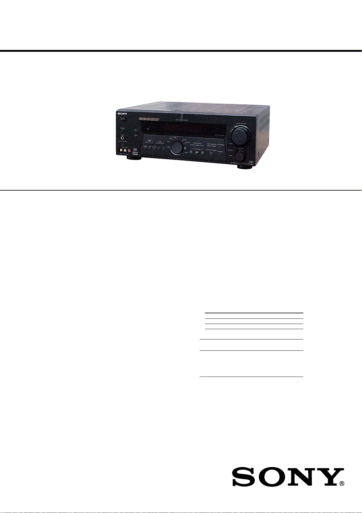
Photo: STR-DE885
This receiver incorporates Dolby* Digital and Pro
Logic Surround and the DTS** Digital Surround
System.
* Manufactured under license from Dolby
Laboratories.
“Dolby”, “Pro Logic” and the double-D symbol are
trademarks of Dolby Laboratories.
** “DTS”, “ES” and “DTS Digital Surround” are
registered trademarks of Digital Theater Systems,
Inc.
US Model
Canadian Model
STR-DE885/DE985
E Model
STR-DE885
AUDIO POWER SPECIFICATIONS
POWER OUTPUT AND TOTAL
HARMONIC DISTORTION:
With 8 ohm loads, both channels driven, from
20 – 20,000 Hz; rated 100 watts per channel
minimum RMS power, with no more than
0.09 % total harmonic distortion from 250
milliwatts to rated output (Models of area
code US only).
Amplifier section
POWER OUTPUT
Models of area code US, CND
Rated Power Output at Stereo Mode
(8 ohms 20 Hz – 20 kHz, THD 0.09 %)
Reference Power Output
(8 ohms 1 kHz, THD 0.7 %)
1)
FRONT
: 100 W/ch
1)
CENTER
SURR
SURR BACK
Models of area code E23, MX
Rated Power Output at Stereo Mode
(8 ohms 1 kHz, THD 0.7 %)
: 100 W
1)
: 100 W/ch
1)
: 100 W (DE985)
100 W + 100 W
100 W + 100 W
2)
2)
SPECIFICATIONS
Reference Power Output
(8 ohms 1 kHz, THD 10 %)
FRONT
CENTER
SURR
1) Depending on the sound field settings and the
source, there may be no sound output.
2) Measured under the following conditions:
Area code Power requirements
E23 240 V AC, 50 Hz
US, CND, MX 120 V AC, 60 Hz
Frequency response
PHONO RIAA equalization curve
MULTI CH IN (1, 2)
CD/SACD, TAPE
MD/DAT
TV/SAT, DVD/LD,
VIDEO 1, 2, 3
2)
1)
: 120 W/ch
1)
: 120 W
1)
: 120 W/ch
±0.5 dB
5)
, 10 Hz – 70 kHz
5)
, +0.5/–2 dB (with sound
5)
, MD/TAPE
6)
,field and equalizer bypassed)
– Continued on next page –
9-874-060-01
2002E0400-1
© 2002. 05
FM STEREO/FM-AM RECEIVER
Sony Corporation
Home Audio Company
Published by Sony Engineering Corporation
1
STR-DE885/DE985
Inputs (Analog)
PHONO Sensitivity: 4 mV
Impedance: 50 kilohms
MULTI CH IN (1, 2)
CD/SACD, TAPE
MD/DAT
5)
, MD/TAPE
5)
3)
S/N
5)
, Sensitivity: 250 mV
, Impedance: 50 kilohms
6)
, S/N
:86 dB (A, 4 mV
3)
: 96 dB (A, 250 mV
4)
)
4)
TV/SAT, DVD/LD,
VIDEO 1, 2, 3
3) INPUT SHORT (with sound field , equaliz er and bass boost
bypassed).
4) Weighted network, input level.
5) STR-DE985
6) STR-DE885
Inputs (Digital)
DVD/LD (Coaxial) Sensitivity: –
Impedance: 75 ohms
S/N: 100 dB
(A, 20 kHz LPF)
CD/SACD, TV/SAT , Sensitivity: –
MD/DAT
5)
, MD/TAPE
6)
, Impedance: –
VIDEO 3 (Optical) S/N: 100 dB
(A, 20 kHz LPF)
Outputs (Analog)
5)
MD/DAT
MD/TAPE
,Voltage: 250 mV
6)
(OUT), Impedance: 10 kilohms
VIDEO1, 2 (AUDIO OUT)
SUB WOOFER, V oltage: 2 V
SURR BACK, Impedance: 1 kilohms
2ND ROOM
5)
Outputs (Digital)
MD/TAPE (Optical) Sensitivity: –
EQ
BASS: 99 Hz – 1.0 kHz
(21 steps)
MID: 198 Hz – 10 kHz
(37 steps)
TREBLE: 1.0 kHz – 10 kHz
(23 steps)
Gain levels: ±10 dB, 1 dB step
FM tuner section
Tuning range 87.5 – 108.0 MHz
Antenna terminals 75 ohms, unbalanced
Intermediate frequency 10.7 MHz
Sensitivity
Mono: 18.3 dBf, 2.2 µV/75 ohms
Stereo: 38.3 dBf, 22.5 µV/75 ohms
Usable sensitivity 11.2 dBf, 1 µV/75 ohms
S/N
Mono: 76 dB
Stereo: 70 dB
Harmonic distortion at 1 kHz
Mono: 0.3%
Stereo: 0.5%
Separation 45 dB at 1 kHz
Frequency response 30 Hz – 15 kHz,
+0.5/–2 dB
Selectivity 60 dB at 400 kHz
AM tuner section
Tuning range
Models of area code US, CND
With 10-kHz tuning scale: 530 – 1710 kHz
With 9-kHz tuning scale: 531 – 1710 kHz
Models of area code E23, MX
With 10-kHz tuning scale: 530 – 1610 kHz
With 9-kHz tuning scale: 531 – 1602 kHz
Antenna Loop antenna
Intermediate Frequency 450 kHz
Usable sensitivity 50 dB/m (at 1,000 kHz or
999 kHz)
S/N 54 dB (at 50 mV/m)
Harmonic distortion 0.5 % (50 mV/m, 400 Hz)
7)
7)
7)
7)
Selectivity
At 9 kHz: 35 dB
At 10 kHz: 40 dB
7) You can change the AM tuning scale to 9 kHz or
10 kHz. After tuning in any AM station, turn off
)
the receiver. Hold down PRESET TUNING + and
press ?/1 . All preset stations will be erased when
you change the tuning scale. To reset the scale to
10 kHz (or 9 kHz), repeat the procedure.
Video section
Inputs
Video: 1 Vp-p, 75 ohms
S-video: Y: 1 Vp-p, 75 ohms
C: 0.286 Vp-p, 75 ohms
Component Video: Y: 1 Vp-p, 75 ohms
PB B-Y: 0.7 Vp-p, 75 ohms
PR R-Y: 0.7 Vp-p, 75 ohms
Outputs
Video: 1 Vp-p, 75 ohms
S-video: Y: 1 Vp-p, 75 ohms
C: 0.286 Vp-p, 75 ohms
Component Video: Y: 1 Vp-p, 75 ohms
PB B-Y: 0.7 Vp-p, 75 ohms
PR R-Y: 0.7 Vp-p, 75 ohms
General
Power requirements
Area code Power requirements
US, CND, MX 120 V AC, 60 Hz
E23 120/220/240 V AC, 50/60 Hz
Power consumption
Area code Power consumption
US STR-DE985: 265 W
CND STR-DE985: 360 VA
MX 210 W
E23 230 W
Power consumption (during standby mode)
AC outlets
Area code AC outlets
US, CND 2 switched, 120 W/1A MAX
E23, MX 1 switched, 100 W MAX
Dimensions 430 × 157.5 × 369 mm
Mass (Approx.) 9.5 kg (20 lb 16 oz)
Supplied accessories
FM wire antenna (1)
AM loop antenna (1)
Remote commander (1)
• RM-PG411 (STR-DE985)
• RM-PP411 (STR-DE885)
R6 (size-AA) batteries (2)
Audio/video/control S cord (1)
Monaural mini-plug cord (1)
Design and specifications are subject to change
without notice.
•Abbreviation
CND : Canadian model
E23 : AC 120/220/240V area in E model
MX : Mexican model
STR-DE885: 210 W
STR-DE885: 300 VA
0.5 W (when “POWER SAVE”
in the CUSTOMIZE menu is
set to “ON”).
(16 7/8 × 6 2/8 × 14 4/8 inches)
including projecting parts
and controls
2
STR-DE885/DE985
SAFETY CHECK-OUT
After correcting the original service problem, perform the following safety check before releasing the set to the customer:
Check the antenna terminals, metal trim, “metallized” knobs, screws,
and all other exposed metal parts for AC leakage.
Check leakage as described below.
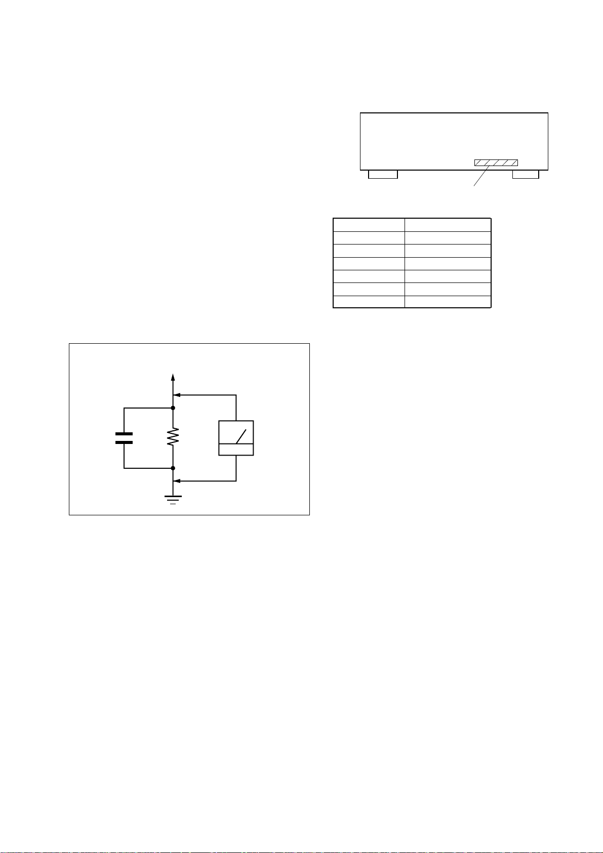
LEAKAGE TEST
The AC leakage from any exposed metal part to earth ground and
from all exposed metal parts to any exposed metal part having a
return to chassis, must not exceed 0.5 mA (500 microampers.).
Leakage current can be measured by any one of three methods.
1. A commercial leakage tester, such as the Simpson 229 or RCA
WT-540A. Follow the manufacturers’ instructions to use these
instruments.
2. A battery-operated AC milliammeter. The Data Precision 245
digital multimeter is suitable for this job.
3. Measuring the voltage drop across a resistor by means of a
VOM or battery-operated AC voltmeter. The “limit” indication is 0.75 V, so analog meters must have an accurate lowvoltage scale. The Simpson 250 and Sanwa SH-63Trd are examples of a passive VOM that is suitable. Nearly all battery
operated digital multimeters that have a 2 V AC range are suitable. (See Fig. A)
To Exposed Metal
Parts on Set
MODEL IDENTIFICATION
— BACK PANEL —
Part No.
Area code Part No.
DE885: US 4-239-124-0s
DE885: CND 4-239-124-1s
DE885: E23 4-239-124-5s
DE885: MX 4-239-124-9s
DE985: US 4-239-222-0s
DE985: CND 4-239-222-1s
1.5 k
0.15 µF
SAFETY-RELATED COMPONENT WARNING!!
COMPONENTS IDENTIFIED BY MARK 0 OR DOTTED LINE
WITH MARK 0 ON THE SCHEMATIC DIAGRAMS AND IN
THE PARTS LIST ARE CRITICAL TO SAFE OPERATION.
REPLACE THESE COMPONENTS WITH SONY PARTS WHOSE
PART NUMBERS APPEAR AS SHO WN IN THIS MANUAL OR
IN SUPPLEMENTS PUBLISHED BY SONY.
Ω
Earth Ground
AC
voltmeter
(0.75 V)
ATTENTION AU COMPOSANT AYANT RAPPORT
À LA SÉCURITÉ!!
LES COMPOSANTS IDENTIFIÉS P AR UNE MARQUE 0 SUR LES
DIAGRAMMES SCHÉMA TIQUES ET LA LISTE DES PIÈCES SONT
CRITIQUES POUR LA SÉCURITÉ DE FONCTIONNEMENT. NE
REMPLACER CES COMPOSANTS QUE PAR DES PIÈCES SONY
DONT LES NUMÉROS SONT DONNÉS DANS CE MANUEL OU
DANS LES SUPPLÉMENTS PUBLIÉS PAR SONY.
3

STR-DE885/DE985
TABLE OF CONTENTS
1. GENERAL
Main unit ................................................................................. 5
Remote button description....................................................... 6
2. DISASSEMBLY
2-1. Case .....................................................................................7
2-2. Front Panel Section ............................................................. 8
2-3. Headphone Board, Opt3 Board, Video3 Board ...................8
2-4. Back Panel Section.............................................................. 9
2-5. Digital Board ....................................................................... 9
2-6. Standby Board ................................................................... 10
2-7. Main Board ....................................................................... 10
3. TEST MODE..................................................................... 11
4. DIAGRAMS
4-1. IC Pin Descriptions ........................................................... 13
4-2. Circuit Boards Location .................................................... 21
4-3. Printed Wiring Boards – Main Section – .......................... 22
4-4. Schematic Diagram – Main Section (1/3) – ...................... 23
4-5. Schematic Diagram – Main Section (2/3) – ...................... 24
4-6. Schematic Diagram – Main Section (3/3) – ...................... 25
4-7. Printed Wiring Board – Digital Section (1/2) – ................ 26
4-8. Printed Wiring Boards – Digital Section (2/2) – ............... 27
4-9. Schematic Diagram – Digital Section (1/4) – ................... 28
4-10. Schematic Diagram – Digital Section (2/4) – ................... 29
4-11. Schematic Diagram – Digital Section (3/4) – ................... 30
4-12. Schematic Diagram – Digital Section (4/4) – ................... 31
4-13. Printed Wiring Board – Speaker Section – ....................... 32
4-14. Schematic Diagram – Speaker Section – .......................... 33
4-15. Printed Wiring Boards – Display Section – ...................... 34
4-16. Schematic Diagram – Display Section –........................... 35
4-17. Printed Wiring Board – Video Section – ........................... 36
4-18. Schematic Diagram – Video Section – .............................. 37
4-19. Printed Wiring Boards – S-video Section – ...................... 38
4-20. Schematic Diagram – S-video Section –........................... 39
4-21. Printed Wiring Board – Component Section –.................. 40
4-22. Schematic Diagram – Component Section – .................... 41
4-23. Printed Wiring Boards – Power Section –......................... 42
4-24. Schematic Diagram – Power Section – ............................. 43
4-25. IC Block Diagrams............................................................ 44
5. EXPLODED VIEWS
5-1. Case Section ...................................................................... 49
5-2. Front Panel Section ...........................................................50
5-3. Chassis Section-1 .............................................................. 51
5-4. Chassis Section-2 .............................................................. 52
6. ELECTRICAL PARTS LIST......................................... 53
4
SECTION 1
GENERAL
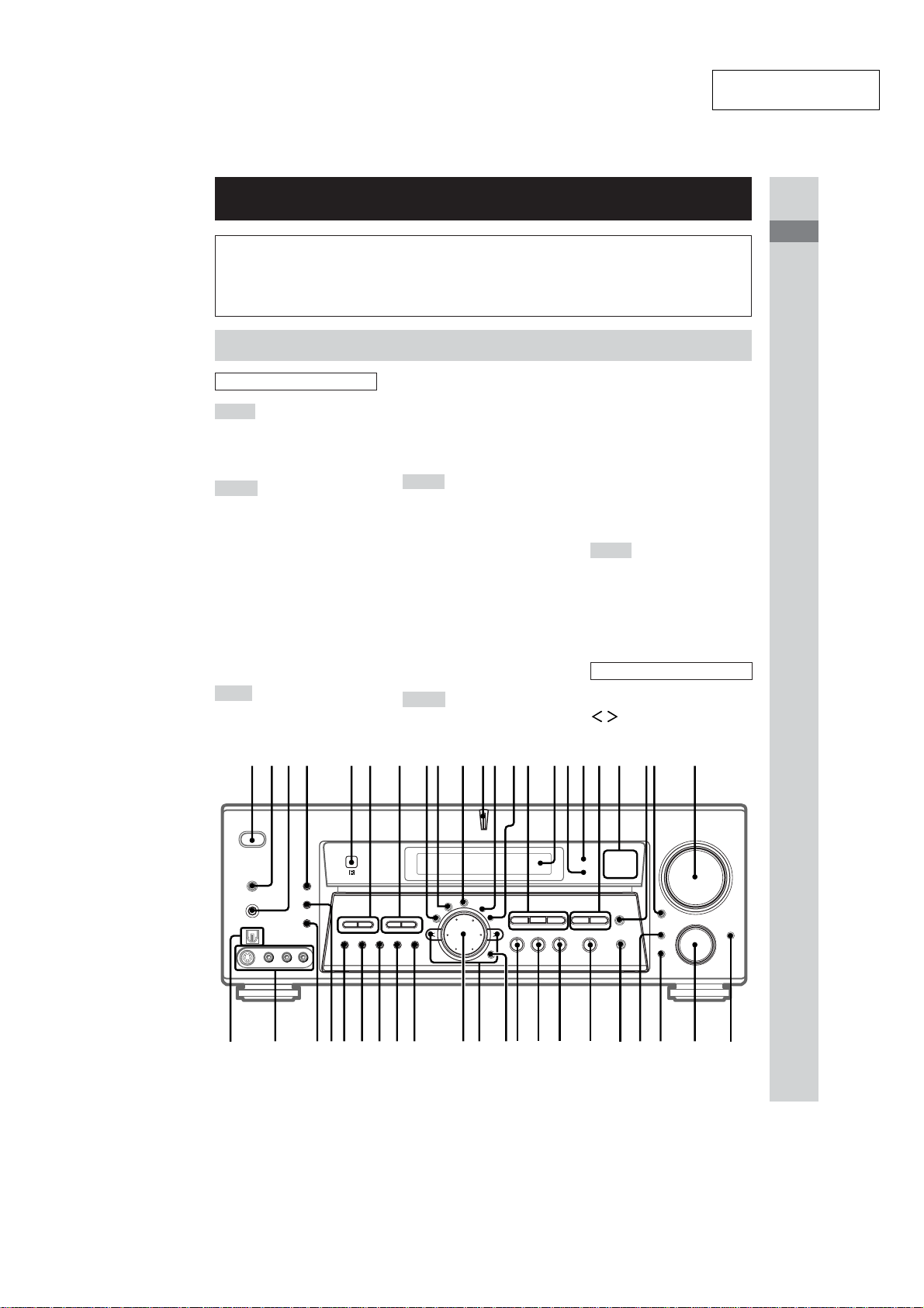
List of Button Locations and Reference Pages
STR-DE885/DE985
This section is extracted
from instruction manual.
How to use this page
Use this page to find the location of buttons that are
mentioned in the text.
Main unit
ALPHABETICAL ORDER
0 — 9
2CH wl (31, 32)
2ND ROOM (STR-DE985 only)
wd (28)
A — D
A. DEC ea (29, 31)
AM eg (40)
CINEMA STUDIO EX A, B, C
qf (30)
CUSTOMIZE qd (42, 44, 65)
Digital Cinema Studio (indicator)
qj (29)
DIGITAL CONCERT HALL A,
B qk (31)
DIMMER r; (28)
DISPLAY 4 (28, 60)
Display qg (28)
E — I
ENTER es (42)
EQ 8 (38, 64)
EQUALIZER wj (38)
FM eh (40)
FM MODE ej (40)
FUNCTION wf (26, 59)
INPUT MODE wh (26)
IR (receptor) 5 (48, 60)
J — N
Jog dial ef (20, 35, 37, 38, 42,
44, 63)
LEVEL q; (25, 37, 63)
MASTER VOLUME ws (25, 58)
MEMORY el (41)
MODE (FUNCTION) wg (26)
MODE (SOUND FIELD) e; (30,
31, 59)
MULTI/2CH ANALOG DIRECT
wk (27)
MULTI CHANNEL DECODING
(indicator) qa (27)
MUTING wa (27, 58)
O — S
ON SCREEN (STR-DE985 only)
ra (10)
Illustration number
r
CUSTOMIZE qd (42, 44, 65)
Name of button/part Reference page
RR
PHONES (jack) 3 (27, 59)
PRESET TUNING +/– 6 (41,
62)
SB DEC (indicator) qh (33)
SET UP qs (20, 65)
SHIFT ek (41)
SPEAKERS A/B 2 (17, 27, 35,
58)
SURR 9 (35, 63)
SURR BACK DECODING w;
(33)
T — Z
TUNING +/– 7 (40)
VIDEO 3 DIGITAL INPUT
(jack) rd (11)
VIDEO 3 INPUT (jacks) rs (10)
VIDEO SELECT INDICATOR
ql (26)
BUTTON DESCRIPTIONS
?/1 (power) 1
/ ed (20, 35, 37, 38, 42, 44,
63)
(19, 25, 39, 62)
List of Button
Locations and
Reference Pages
1234 56 7 89 q;qaqsqdqfqgqhqjqkql w ;wa ws
wj
wkwle;eaesedefegehejekelr;rarsrd
wgwh
wf
wd
GB
5
5
STR-DE885/DE985
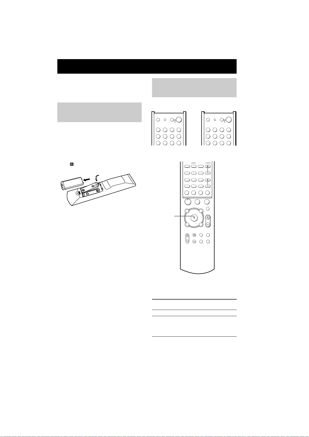
Operations Using the Remote RM-PG411 and RM-PP411
You can use the remote RM-PG411 (STRDE985 only) or RM-PP411 (STR-DE885 only)
to operate the components in your system.
Before you use your
remote
Inserting batteries into the
remote
Insert R6 (size-AA) batteries with the + and –
properly oriented in the battery compartment.
When using the remote, point it at the remote
sensor on the receiver.
Tip
Under normal conditions, the batteries should last for
about 6 months. When the remote no longer operates
the receiver, replace all batteries with new ones.
Notes
• Do not leave the remote in an extremely hot or
humid place.
• Do not use a new battery with an old one.
• Do not expose the remote sensor to direct sunlight
or lighting apparatuses. Doing so may cause a
malfunction.
• If you don’t use the remote for an extended period
of time, remove the batteries to avoid possible
damage from battery leakage and corrosion.
Remote button description
RM-PG411 RM-PP411
USE MODE
SYSTEM STANDBY
TAPE MD/DAT
M2
PHONO
?/1
P
SLEEP
VIDEO3 DVD/LD
CD/SACD
MULTI CH SOURCE
TV ?/1 AV ?/1
VIDEO1 VIDEO2
AV1 AV2
TV/SAT
PHONO AUX
TV ?/1 AV ?/1
VIDEO1 VIDEO2
AV1 AV2 2ND
TV/SAT
M1
TIMER
RM-PG411 and RM-PP411
SOUND FIELD
TEST
TONE
PRESET
AUTO DEC
123
MPX/
DUAL
456
AUDIO
789
.
0/10 >10/11 12
SHIFT
m
ANT
N
TOP MENU/
ENTER/
EXECUTE
GUIDE
G
DISPLAY
TV VOL TV CH
The tables below show the settings of each
button common to both remote RM-PG411 and
RM-PP411.
Remote Operations Function
Button
?/1 Receiver
SLEEP Receiver Activates the sleep
MODE
ANALOG
DIRECT
2CH
SWAP/
JUMP/
PRESET/
ANGLE
TIME
CH/D.SKIP
SUBTITLE ENTER
>
D.TUNING DISC ALT
-
M
CLEAR
SEARCH MODE
X
x
MUTING
AV MENU
MASTER
F
VOL
g
f
O
RETURN/EXIT
TV/
MAIN
VIDEO
MENU
WIDE ON SCREEN
Turns the receiver on or off.
function and the duration
which the receiver turns
off automatically.
USE MODE
SYSTEM STANDBY
MD/TAPE CD/SACD
MULTI CH SOURCE
?/1
P
SLEEP
VIDEO3 DVD/LD
TUNER
US
48
6
SECTION 2
)
DISASSEMBLY
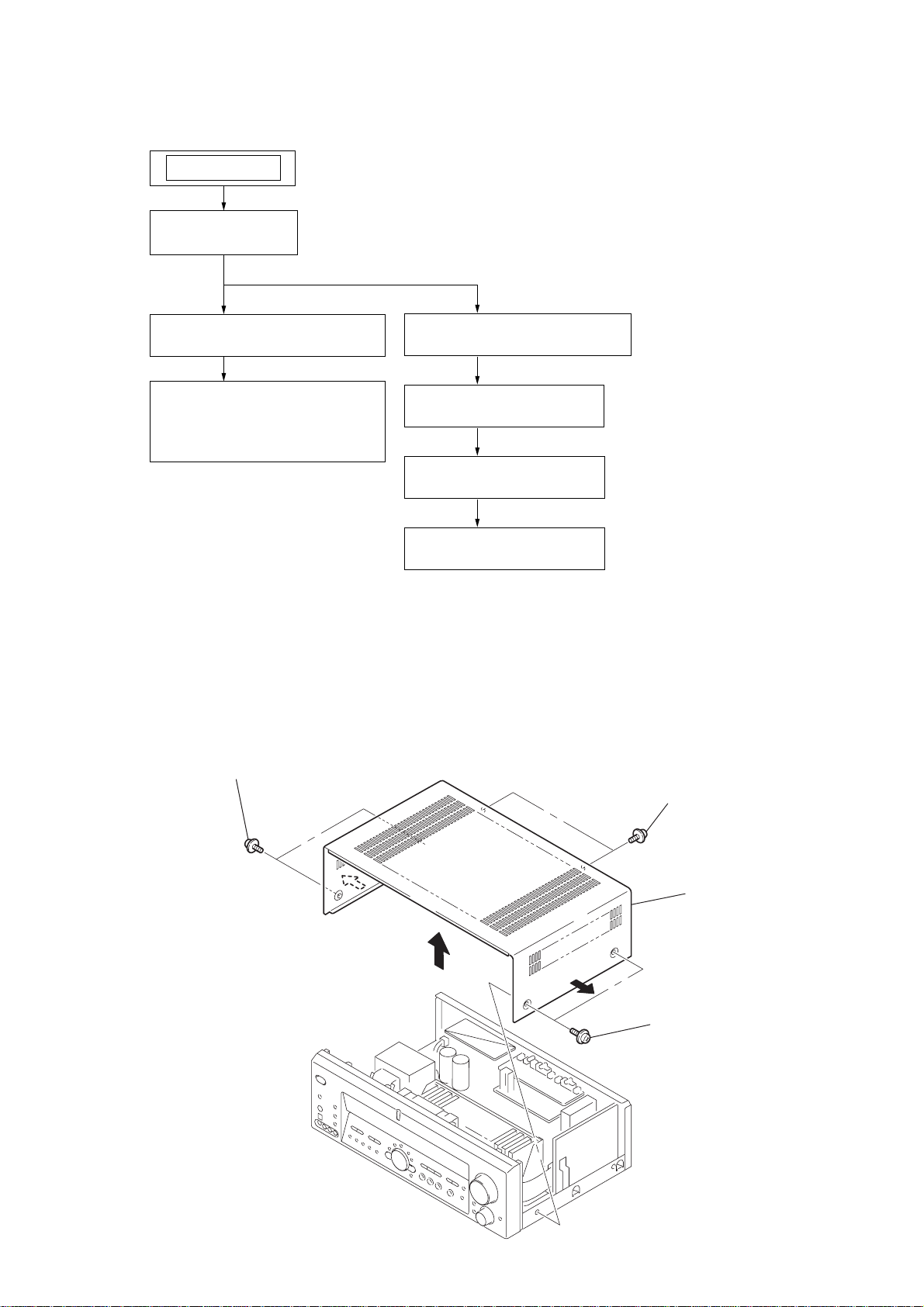
Note : This set can be disassemble according to the following sequence.
SET
2-1. CASE
(Page 7)
STR-DE885/DE985
2-2. FRONT PANEL SECTION
(Page 8)
2-3. HEADPHONE BOARD,
OPT3 BOARD,
2-4. BACK PANEL SECTION
(Page 9)
2-5. DIGITAL BOARD
(Page 9)
VIDEO3 BOARD
(Page 8)
2-6. STANDBY BOARD
(Page 10)
2-7. MAIN BOARD
(Page 10)
Note : Follow the disassembly procedure in the numerical order given.
2-1. CASE
1
two screws
(case 3 TP2)
2
two screws
(case 3 TP2
4
3
two screws
(case 3 TP2)
case
7
STR-DE885/DE985
)
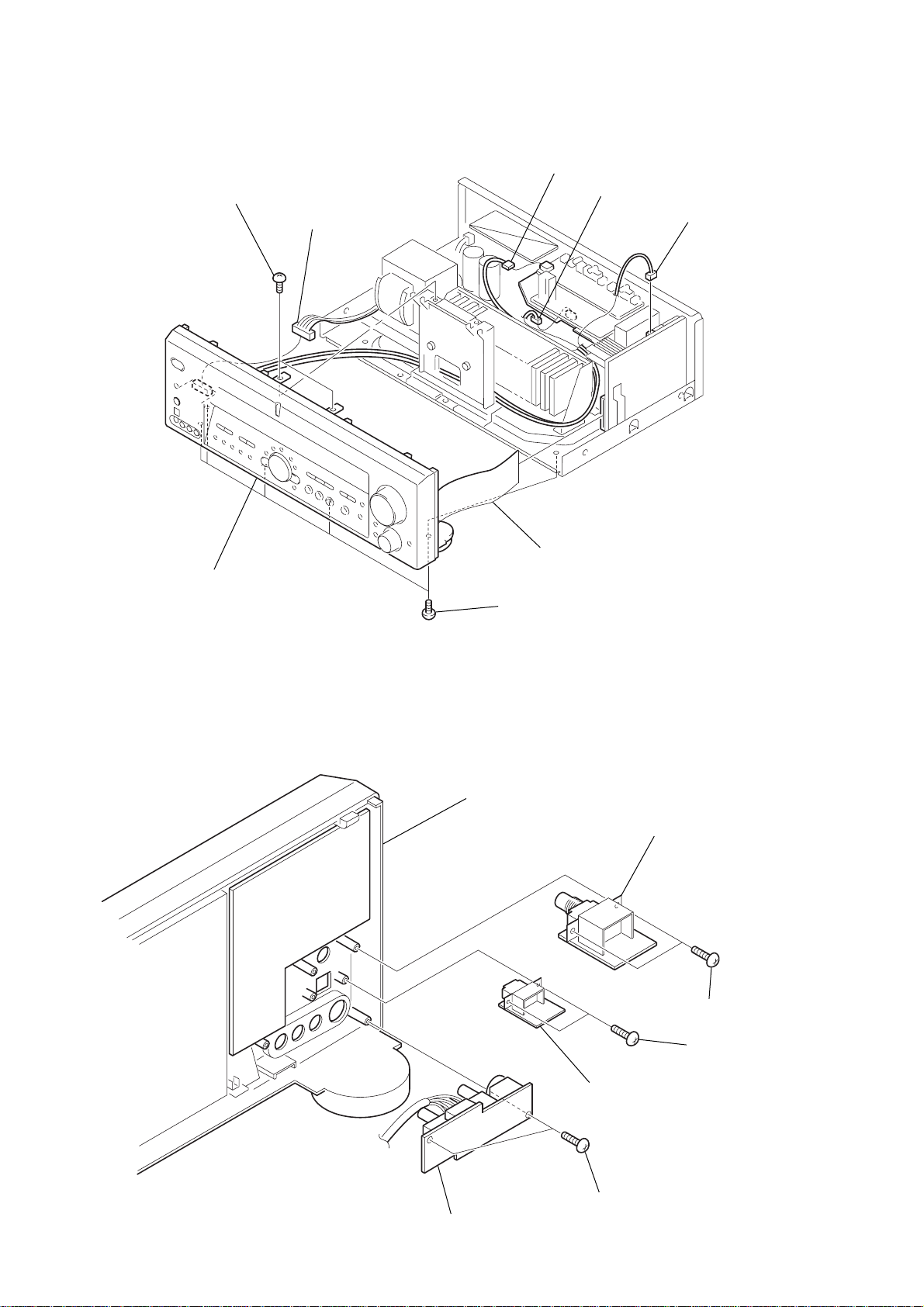
2-2. FRONT PANEL SECTION
6
two screws
(BVTP 3x8)
2
CNP701
4
CNP205
5
CNP210
3
CNP508
8
front panel section
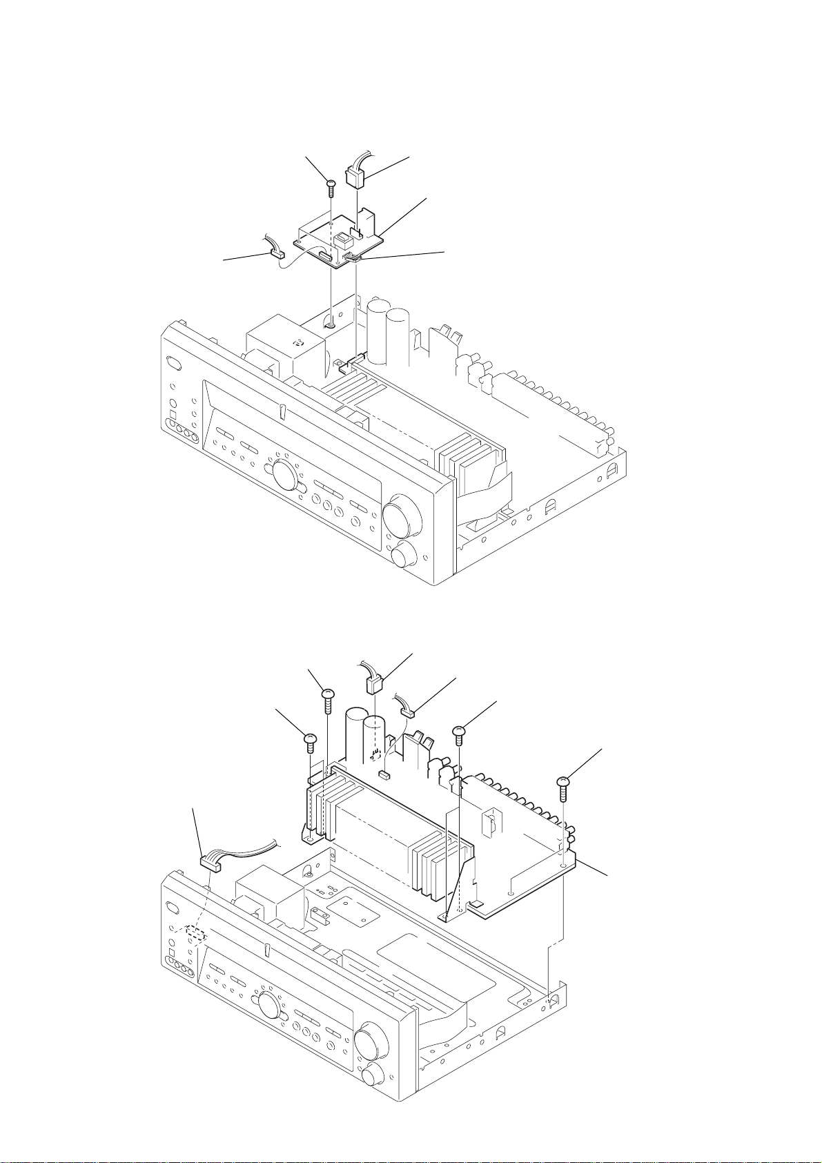
2-3. HEADPHONE BOARD, OPT3 BOARD, VIDEO3 BOARD
1
CNS505
7
five screws
(BVTP 3x8)
front panel section
2
HEADPHONE board
1
two screws
(BVTP 2.6x8
3
two screws
(BVTP 2.6x8)
4
4
VIDEO3 board
OPT3 board
3
two screws
(BVTP 2.6x8)
8
2-4. BACK PANEL SECTION
s
3
CNP901
4
CN808
(DE985)
0
CNP205
qd
two screws
(BVTP 3x8)
9
CNP207
8
CNP210
STR-DE885/DE985
2
CNS509
qa
five screws
(BVTP 3x8)
qs
eleven screw
(BVTP 3x8)
qf
four screws
(BVTP 3x8)
5
CN807
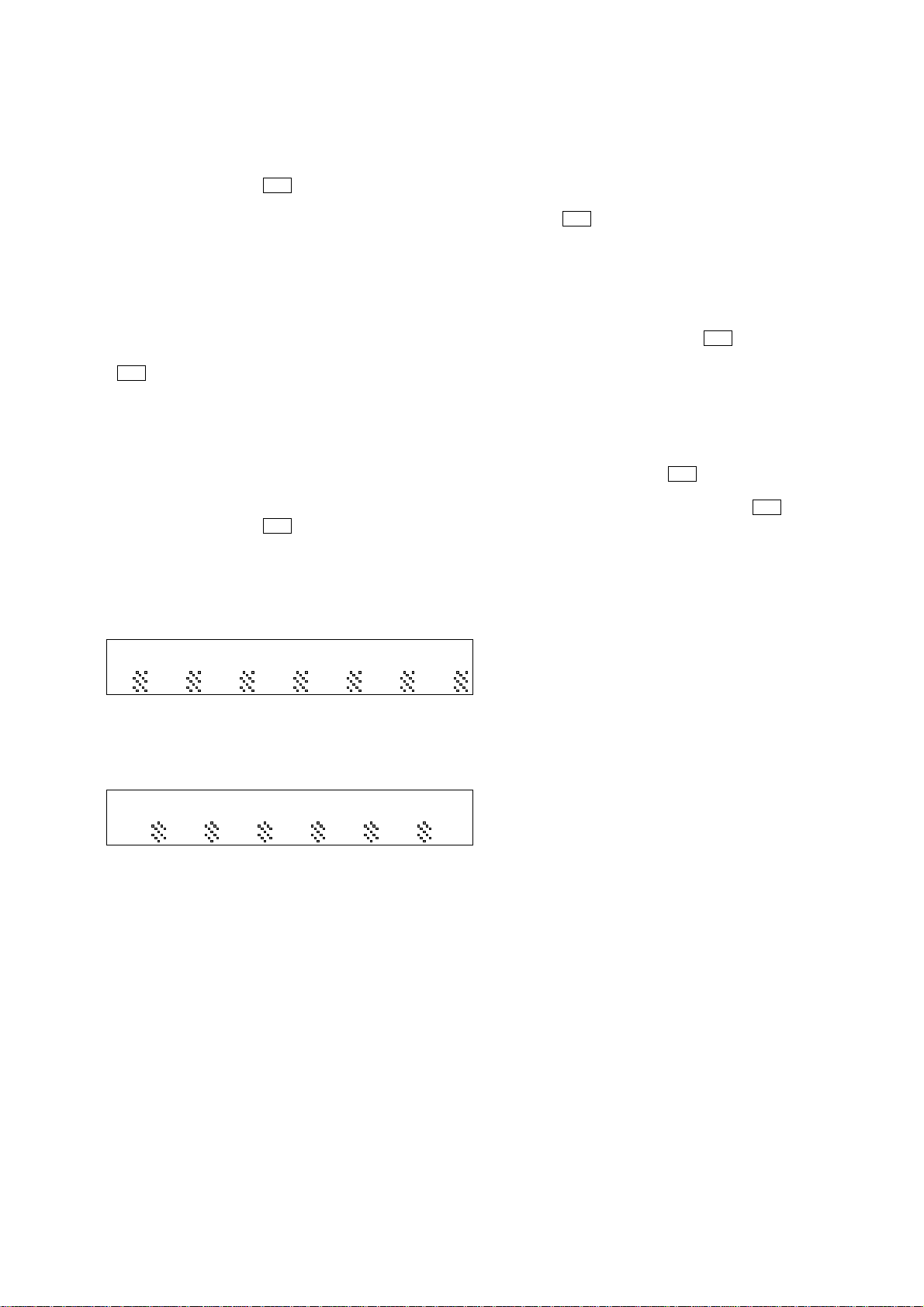
2-5. DIGITAL BOARD
0
screw (BVTP 3x8)
5
6
4
CNP507
CNP812
CNP506
3
1
7
CNP814
CNP509
CNS508
2
qg
back panel
CNP508
7
CNS502
8
CNS501
9
DIGITAL board
1
CNS505
qa
bracket (DIGITAL)
6
screw (BVTP 3x8)
9
STR-DE885/DE985
2-6. STANDBY BOARD
3
CNP815
4
three screws
(BVTP 3x8)
2
CNP905
5
STANDBY board
1
CNP813
2-7. MAIN BOARD
5
two screws
(BVTP 3x6)
1
CNP701
6
two screws
(BVTP 3x8)
2
CNP801
3
CNP802
4
two screws
(BVTP 3x6)
7
two screws
(BVTP 3x8)
8
MAIN board
10
SECTION 3
TEST MODE
STR-DE885/DE985
FACTORY PRESET MODE
* All preset contents are reset to the default setting.
* Procedure:
While depressing the [SET UP] and the [DIMMER] buttons simultaneously, press the po wer
The message “TUNER FACTORY PRESET” appears and the
present contents are reset to the default values.
?/1 button to turn on the main power.
AM CHANNEL STEP 9 KHZ/10 KHZ
SELECTION MODE
* Either the 9 kHz step or 10 kHz step can be selected for the AM
channel step.
* Procedure:
Set the FUNCTION to AM. Turn off the main power.
While depressing the [PRESET TUNING+] button, press the power .
?/1 button to turn on the main power. Either the message 9 k
STEP or 10 k STEP appears. Select the desired step.
FLUORESCENT INDICATOR TUBE TEST MODE
* All fluorescent segments are tested. When this test is acti v ated ,
all segments turn on at the same time, then each segment turns
on one after another.
* Procedure:
While depressing the [A.DEC] and the [DIMMER] buttons simultaneously, press the po wer ?/1 button to turn on the main power .
1. All segments turn on.
[VIDEO 2], [SETUP], [DVD/LD], [MULTI CHANNEL DECODING]
(blue) and [MULTI/2CH ANALOG DIRECT] LEDs turn on.
SOUND FIELD CLEAR MODE
*The preset sound field is cleared when this mode is activated.
Use this mode before returning the product to clients upon
completion of repair.
* Procedure:
While depressing the [SOUND FIELD MODE] button, press the
power ?/1 button to turn on the main power. The message
“S.F Initialize” appears and initialization is performed.
VERSION DISPLAY MODE
*The version is displayed.
* Procedure:
While depressing the [MUTING] and the [DIMMER] buttons
simultaneously, press the po wer ?/1 button to turn on the main
power. The massage “VERSION” and the version number are
displayed.
KEY CHECK MODE
* Button check
* Procedure:
While depressing the [LEVEL] and the [DISPLAY] buttons simultaneously, press the po wer ?/1 button to turn on the main power .
“Rest 36 Key” appears.
Every pressing of any button other than ?/1 counts down the
buttons. The buttons which are already counted once are not
counted again. When all buttons are pressed “Rest 00 Key”
appears.
2. Press the [A.DEC] or the [DIMMER] button, confirm display.
(Display)
[SOUND FIELD MODE], [VIDEO 1], [VIDEO 3], [SOUND FIELD
2CH], [SURR] and [A.DEC] LEDs turn on.
3. Press the [A.DEC] or the [DIMMER] button, confirm display.
(Display)
[Digital Cinema Sound], [TV/SAT], [LEVEL], [EQ], [CUSTOMIZE]
and [A.DEC] LEDs turn on.
4. Press the [A.DEC] or the [DIMMER] button, All segments turn
off. ALL LEDs turn off.
5. Every pressing of the [A.DEC] or the [DIMMER] button turns on
each segment and LED one after another in the same order.
11

STR-DE885/DE985
MEMO
12
STR-DE885/DE985
SECTION 4
DIAGRAMS
4-1. IC PIN DESCRIPTIONS
• IC1501 CXD9617R (AUDIO DSP1) (DIGITAL Board (2/4))
Pin No. Pin Name I/O Pin Description
1 VSS — Ground
2 XRST I Reset signal input
3 EXTIN I Not used (connected to ground)
4 FS2 I Sampling frequency select signal input (connected to ground)
5 VDDI — Power supply pin (+2.5 V)
6 FS1 I Sampling frequency select signal input (connected to ground)
7 PLOCK O Internal PLL lock signal output (Not used (open))
8 VSS — Ground
9 MCLK1 I System clock signal input (13.5 MHz)
10 VDDI — Power supply pin (+2.5 V)
11 VSS — Ground
12 MCLK2 O System clock signal output (13.5 MHz)
13 MS I Master/slave operation select signal input (L : internal clock, H : EXTIN clock)
14 SCKOUT O Serial clock signal output
15 LRCKI1 I L/R sampling clock signal input (Not used (open))
16 VDDE — Power supply pin (+3.3 V)
17 BCKI1 I Bit clock signal input (Not used (open))
18 SDI1 I Audio serial data input
19 LRCKO O L/R sampling clock signal output
20 BCKO O Bit clock signal output
21 VSS — Ground
22 KFSIO I/O Audio clock signal (384fs/256fs) input/output
23 to 26 SDO1 to SDO4 O Audio serial data output
27 SPDIF O S/PDIF output (Not used (open))
28 LRCKI2 I L/R sampling clock signal input
29 BCKI2 I Bit clock signal input
30 SDI2 I Audio serial data input
31 VSS — Ground
32 HACN O Host acknowledge signal output
33 HDIN I Host serial data input
34 HCLK I Host clock signal input
35 HDOUT O Host serial data output
36 HCS I Host chip select input
37 SDCLK O Not used (open)
38 CLKEN O Not used (open)
39 RAS O Row address strobe signal output (Not used (open))
40 VDDI — Power supply pin (+2.5 V)
41 VSS — Ground
42 CAS O Column address strobe signal output (Not used (open))
43 DQM/OE0 O Not used (open)
44 CS0 O Chip select signal output
45 WE0 O Write enable signal output
46 VDDE — Power supply pin (+3.3 V)
47 WMD1 I External memory wait mode setting signal input (connected to H)
48 VSS — Ground
49 WMD0 I External memory wait mode setting signal input (connected to ground)
50 PAGE2 O External memory page select signal output (Not used (open))
51 VSS — Ground
52, 53 PAGE1, PAGE0 O External memory page select signal output (Not used (open))
54 BOOT I Boot mode control signal input (connected to ground)
55 BTACT O Boot mode display signal output (Not used (open))
13

STR-DE885/DE985
Pin No. Pin Name I/O Pin Description
56 BST I Boot stop signal input
57 MOD1 I Mode select signal input (L : 384fs, H : 256fs)
58 MOD0 I Mode select signal input (L : single chip mode, H : use prohibited)
59 EXLOCK I External lock signal input
60 VDDI — Power supply pin (+2.5 V)
61 VSS — Ground
62, 63 A17, A16 O Address signal output (Not used (open))
64 to 66 A15 to A13 O Address signal output (SRAM)
67 GP10 O L/R sampling clock signal output
68 GP9 O GP9 signal output
69 GP8 I Audio signal input
70 VDDI — Power supply pin (+2.5 V)
71 VSS — Ground
72 to 75 D15/GP7 to D12/GP4 I/O External memory data input/output (general port)
76 VDDE — Power supply pin (+3.3 V)
77 to 80 D11/GP3 to D8/GP0 I/O External memory data input/output (general port)
81 VSS — Ground
82 A9 O Address signal output (SRAM)
83 to 85 A12 to A10 O Address signal output (SRAM)
86 TDO O Emulation data output (Not used (open))
87 TMS I Emulation start/end select data input (Not used (open))
88 XTRST I Emulation break signal input (Not used (open))
89 TCK I Emulation clock signal input (Not used (open))
90 TDI I Emulation data input (Not used (open))
91 VSS — Ground
92 to 97 A8 to A3 O Address signal output (SRAM)
98, 99 D7, D6 I/O External memory data input/output (SRAM)
100 VDDI — Power supply pin (+2.5 V)
101 VSS — Ground
102 to 105 D5 to D2 I/O External memory data input/output (SRAM)
106 VDDE — Power supply pin (+3.3 V)
107, 108 D1, D0 I/O External memory data input/output (SRAM)
109, 110 A2, A1 O Address signal output (SRAM)
111 VSS — Ground
112 A0 O Address signal output (SRAM)
113 PM I PLL initialization signal input
114, 115 SDI3, SDI4 I Audio serial data input (Not used (open))
116 SYNC I Sync/unsync select signal input (L : sync, H : unsync)
117 to 119 VSS — Ground
120 VDDI — Power supply pin (+2.5 V)
14
STR-DE885/DE985
• IC1551 CXD9616R (AUDIO DSP2) (DIGITAL Board (3/4))
Pin No. Pin Name I/O Pin Description
1 VDDI — Power supply pin (+2.5 V)
2 EXTIN I Not used (connected to ground)
3, 4 WMD1, WMD0 I External memory wait mode setting signal input (connected to H)
5 MOD1 I Mode select signal input (L : 384fs, H : 256fs)
6 MOD0 I Mode select signal input (L : single chip mode, H : use prohibited)
7 VSS — Ground
8 XRST I Reset signal input
9 VSS — Ground
10 SCKOUT O Serial clock signal output
11 VDDI (PLL) — Power supply pin (+2.5 V) (for PLL)
12 SYNC I Sync/unsync select signal input (L : sync, H : unsync)
13 to 15 PAGE2 to PAGE0 O External memory page select signal output (Not used (open))
16 PLOCK O Internal PLL lock signal output
17 BTACT O Boot mode display signal output (Not used (open))
18 VDDE — Power supply pin (+3.3 V)
19 VSS — Ground
20 to 22 D31 to D29 I/O External memory data input/output (SRAM)
23 A17 O Address signal output (Not used (open))
24 VSS — Ground
25, 26 SDO3, SDO4 O Audio serial data output
27, 28 SDI1, SDI2 I Audio serial data input
29 LRCKI1 I L/R sampling clock signal input
30 VSS — Ground
31, 32 D28, D27 I/O External memory data input/output (SRAM)
33 A16 O Address signal output (Not used (open))
34 A15 O Address signal output (SRAM)
35 SDI3 I Audio serial data input
36 L2 O Not used (open)
37 VDDI — Power supply pin (+2.5 V)
38 BCKI1 I Bit clock signal input
39 SDI4 I Audio serial data input
40 MS I Master/slave operation select signal input (L : internal clock, H : EXTIN clock)
41, 42 A14, A13 O Address signal output (SRAM)
43, 44 D26, D25 I/O External memory data input/output (SRAM)
45 VSS — Ground
46 BCKI2 I Bit clock signal input (Not used (open))
47, 48 FS2, FS1 I Sampling frequency select signal input (connected to ground)
49 SPDIF O S/PDIF output (Not used (open))
50 A12 O Address signal output (SRAM)
51 to 53 D24 to D22 I/O External memory data input/output (SRAM)
54 VDDE — Power supply pin (+3.3 V)
55 VSS — Ground
56 to 58 D21 to D19 I/O External memory data input/output (SRAM)
59 A11 O Address signal output (SRAM)
60, 61 SDO1, SDO2 O Audio serial data output
62 KFSIO I/O Audio clock signal (384fs/256fs) input/output
63 LRCKO O L/R sampling clock signal output
64 BCKO O Bit clock signal output
65 VDDI — Power supply pin (+2.5 V)
66 VSS — Ground
67, 68 D18, D17 I/O External memory data input/output (SRAM)
69, 70 A10, A9 O Address signal output (SRAM)
15

STR-DE885/DE985
Pin No. Pin Name I/O Pin Description
71 CAS O Column address strobe signal output
72 RAS O Row address strobe signal output
73 VDDI — Power supply pin (+2.5 V)
74 HDIN I Host serial data input
75 HCLK I Host clock signal input
76 HCS I Host chip select input
77, 78 A8, A7 O Address signal output (SRAM)
79 D16 I/O External memory data input/output (SRAM)
80 D15 I/O External memory data input/output (SRAM) (Not used (open))
81 VSS — Ground
82 HDOUT O Host serial data output
83 HACN O Host acknowledge signal output
84 CS0 O Chip select signal output
85 WE0 O Write enable signal output
86 A6 O Address signal output (SRAM)
87 to 89 D14 to D12 I/O External memory data input/output (SRAM) (Not used (open))
90 VDDE — Power supply pin (+3.3 V)
91 VSS — Ground
92 to 94 D11 to D9 I/O External memory data input/output (SRAM) (Not used (open))
95 A5 O Address signal output (SRAM)
96 VDDI — Power supply pin (+2.5 V)
97 TCK I Emulation clock signal input (Not used (open))
98 TDI I Emulation data input (Not used (open))
99 TDO O Emulation data output (Not used (open))
100 TMS I Emulation start/end select data input (Not used (open))
101 XTRST I Emulation break signal input (Not used (open))
102 VSS — Ground
103, 104 D8, D7 I/O External memory data input/output (SRAM) (Not used (open))
105, 106 A4, A3 O Address signal output (SRAM)
107, 108 GP10, GP9 — Not used (open)
109 VDDI — Power supply pin (+2.5 V)
110 GP8 — Not used (open)
111 GP7 I Serial clock signal input
112 GP6 — Not used (open)
113, 114 A2, A1 O Address signal output (SRAM)
115, 116 D6, D5 I/O External memory data input/output (SRAM) (Not used (open))
117 VSS — Ground
118, 119 GP5, GP4 — Not used (open)
120 GP3 O Error signal output
121 NC — Not used (open)
122 A0 O Address signal output (SRAM)
123 to 125 D4 to D2 I/O External memory data input/output (SRAM) (Not used (open))
126 VDDE — Power supply pin (+3.3 V)
127 VSS — Ground
128, 129 D1, D0 I/O External memory data input/output (SRAM) (Not used (open))
130 GP2 — Not used (open)
131 GP1 I Clock signal input
132 GP0 I Serial clock signal input
133 SDCLK O Not used (open)
134 CLKEN O Not used (open)
135 DQM O Not used (open)
136 EXLOCK I External lock signal input
16

Pin No. Pin Name I/O Pin Description
137 VDDI — Power supply pin (+2.5 V)
138 VSS — Ground
139 MCLK2 O System clock signal output (13.5 MHz)
140 PM I PLL initialization signal input
141 BST I Boot stop signal input
142 BOOT I Boot mode control signal input (connected to ground)
143 TST I Not used (open)
144 MCLK1 I System clock signal input (13.5 MHz)
STR-DE885/DE985
17

STR-DE885/DE985
• IC1101 MB91154PFV-G-106-BNDE1 (SYSTEM CONTROLLER) (DIGITAL Board (4/4))
Pin No. Pin Name I/O Pin Description
1 6.1_LAT O MULTI CH IN SW IC
2 6.1_DATA O MULTI CH IN SW IC
3 6.1_CLK O MULTI CH IN SW IC
4 V_AUDIO_LAT O VIDEO (AU) SW CONTROL
5 LED_DRV_DATA O LED DRIVER IC
6 LED_DRV_CLK O LED DRIVER IC
7 LED_DRV_CLR O LED DRIVER IC
8 LED_DRV_CE O LED DRIVER IC
9 VSS — Ground
10 CURSOR_JOG_3A I CURSOR JOG ENCODER
11 CURSOR_JOG_3B I CURSOR JOG ENCODER
12 FUNCTION_JOG_1A I FUNCTION JOG ENCODER
13 FUNCTION_JOG_1B I FUNCTION JOG ENCODER
14 VOL_JOG_2B I VOLUME JOG ENCODER
15 VOL_JOG_2A I VOLUME JOG ENCODER
16 SPK_SEL I SPEAKER SELECT SW
17 SP_B_RY O SPEAKER B RELAY
18 HP_RY O HP RELAY CONTROL
19 SP_A_RY O FRONT CH RELAY CONTROL
20 CENTER_RY O CENTER RELAY CONTROL
21 REAR_RY O REAR CH RELAY CONTROL
22 WOOFER_RY O WOOFER RELAY CONTROL
23 PROTECTOR I PROTECTOR CIRCUIT
24 HP_CTRL I HP DETECTION SW
25 PW_RY O POWER RELAY CONTROL
26 VSS — Ground
27 VCC — Power supply pin (+3.2 V)
28 TUNER_STEREO I TUNER PACK
29 TUNER_AUTO_STOP I TUNER PACK
30 TUNER_MUTE O TUNER PACK
31 TUNER_DO I TUNER PACK
32 T.SERIAL_CLK O TUNER PACK
33 T.DATA O TUNER PACK
34 T.LAT O TUNER PACK
35 RDS_DATA I TUNER PACK
36 to 39 V.SW1 to V.SW4 O VIDEO SWITCHING IC
40 PRE OUT RY O PRE OUT RELAY CONTROL
41 SUB-T O SUB TRANSFORMER VOLT O/P
42 TC74HC153_A O OPTICAL INPUT SW
43 DIR XMODE O DIR IC
44 VSS — Ground
45 DIR CKSEL1 O DIR IC
46 DIR CLK O DIR IC
47 DSP1.HDOUT1 I AUDIO DSP1 IC
48 DSP1.PLL1 I AUDIO DSP1 IC
49 DSP2.GP3 I AUDIO DSP2 IC
50 DSP2.EXLOCK O AUDIO DSP2 IC
51 MBUS_STATUS_OUT O MBUS IC
52 MD2 — FLASH PROGRAMMING
53 MD1 — FLASH PROGRAMMING
54 MD0 — FLASH PROGRAMMING
55 RSTX I RESET IC
18
Pin No. Pin Name I/O Pin Description
56 VCC — Power supply pin (+3.2 V)
57 X1 I System clock signal input (16.5 MHz)
58 X0 O System clock signal output (16.5 MHz)
59 VSS — Ground
60 VOLT_DETECT_STOP I VOLTAGE DOWN DETECT
61 RDS_INT I TUNER PACK
62 PW_ON/OFF I POWER SW
63 MBUS_TV I MBUS IC
64 MBUS_DVD I MBUS IC
65 MBUS_VIDEO I MBUS IC
66 SIRCS I REMOTE SENSOR
67 DIR CE O DIR IC
68 VCC — Power supply pin (+3.2 V)
69 DI I DIR IC
70 D.DO O DIR IC
71 ERROR I DIR IC
72 9617.XRST1 O AUDIO DSP1 IC
73 9617.PM1 O AUDIO DSP1 IC
74 9617.GP9 I AUDIO DSP1 IC
75 9617.BST1 O AUDIO DSP1 IC
76 9617.HCS1 O AUDIO DSP1 IC
77 VCC — Power supply pin (+3.2 V)
78 9617.HACN1 I AUDIO DSP1 IC
79 DATA0 I DIR IC
80 XSTATE I DIR IC
81 9616.BST2 O AUDIO DSP2 IC
82 9616.PM2 O AUDIO DSP2 IC
83 9616.XRST2 O AUDIO DSP2 IC
84 9616.HACN2 I AUDIO DSP2 IC
85 9616.HCS2 O AUDIO DSP2 IC
86 A1 IN I CONTROL A1 CIRCUIT
87 A1 OUT O CONTROL A1 CIRCUIT
88 PCM1800.RST O A/D IC
89 PCM1604.RST O D/A IC
90 PCM1604.ML O D/A IC
91 PCM1604.MC O D/A IC
92 PCM1604.MD1 O D/A IC
93 PCM1604.MD0 I D/A IC
94 FLASH_A/FREQ_SEL O DIR IC
95 FLASH_B/TC74HC153_B O OPTICAL INPUT SW
96 FLASH_C I SECONDARY FUSE DETECT
97 VCC — Power supply pin (+3.2 V)
98 VSS — Ground
99 EEPROM.SDA I/O EEPROM
100 EEPROM.SCL I/O EEPROM
101 VSS — Ground
102 9616.HCLK2 O AUDIO DSP2 IC
103 HDIN2 O AUDIO DSP2 IC
104 HDOUT2 I AUDIO DSP2 IC
105 OSD_CLK O OSD CIRCUIT
106 OSD_DATA O OSD CIRCUIT
107 OSD_LAT O OSD CIRCUIT
STR-DE885/DE985
19
STR-DE885/DE985
Pin No. Pin Name I/O Pin Description
108 PLL2 I AUDIO DSP2 IC
109 SOTI I FLASH PROGRAMMING
110 SINI O FLASH PROGRAMMING
111 FL_CLK O FL DRIVER IC
112 FL_DIN O FL DRIVER IC
113 FL_LAT O FL DRIVER IC
114 FL_CLR O FL DRIVER IC
115 PCM1748_ML O D/A IC
116 VOL_IC.DATA O VOL IC
117 VOL_IC.CLK O VOL IC
118 VOL_IC.LAT O VOL IC
119 AC_MUTE O A-CLASS IC
120 SYSTEM_MUTE O MUTING CIRCUIT
121 2ND_RY O 2ND ROOM RELAY CONTROL
122 VCC — Power supply pin (+3.2 V)
123 to 125 DA2 to DA0 — Not used (open)
126 DAVS — Ground
127 DAVC — Power supply pin (+3.2 V)
128 AVCC — Power supply pin (+3.2 V)
129 AVRH — Power supply pin (+3.2 V)
130 AVRL — Ground
131 AVSS — Ground
132 to 136 AD1 to AD5 I DISPLAY
137 MODEL I Destination (MODEL) initial setting input
138 AREA I Destination (AREA) initial setting input
139 RDS_SIGNAL I TUNER PACK
140 VCC2 — Power supply pin (+3.2 V)
141 BACKUP — Power supply pin (+3.2 V)
142 X0A O Not used (connected to ground)
143 X1A I Not used (open)
144 VSS — Ground
20
STR-DE885/DE985
d
4-2. CIRCUIT BOARDS LOCATION
STANDBY board
POWER board
HEADPHONE board
OPT3 board
VIDEO3 board
JOG board
AC SELECT board
SPEAKER board
DISPLAY board
S-VIDEO board
MAIN board
VIDEO board
DIGITAL boar
COMPONENT board
THIS NOTE IS COMMON FOR PRINTED WIRING
BOARDS AND SCHEMATIC DIAGRAMS.
(In addition to this, the necessary note is
printed in each block.)
for schematic diagram:
• All capacitors are in µF unless otherwise noted. pF: µµF
50 WV or less are not indicated except for electrolytics
and tantalums.
• All resistors are in Ω and 1/
specified.
f
•
• 2 : nonflammable resistor.
• 5 : fusible resistor.
• C : panel designation.
• A : B+ Line.
• B : B– Line.
•Voltage and waveforms are dc with respect to ground
•Voltages are taken with a VOM (Input impedance 10 M Ω).
•Waveforms are taken with a oscilloscope.
• Circled numbers refer to waveforms.
• Signal path.
•Abbreviation
: internal component.
Note:
The components identified by mark 0 or dotted
line with mark 0 are criti-
cal for safety.
Replace only with part
number specified.
under no-signal (detuned) conditions.
no mark : FM
Voltage variations may be noted due to normal production tolerances.
Voltage variations may be noted due to normal production tolerances.
F : TUNER (FM/AM)
L : VIDEO (AUDIO)
I : VIDEO
J : CD (ANALOG)
c : CD (DIGITAL)
CND : Canadian model.
E23 : AC 120/220/240V area in E model.
MX : Mexican model.
4
W or less unless otherwise
Note:
Les composants identifiés par
une marque 0 sont critiques
pour la sécurité.
Ne les remplacer que par une
piéce portant le numéro
spécifié.
for printed wiring boards:
• X : parts extracted from the component side.
f
•
• : Pattern from the side which enables seeing.
Caution:
Pattern face side: Parts on the pattern face side seen from the
(Side B) pattern face are indicated.
Parts face side: Parts on the parts face side seen from the
(Side A) parts face are indicated.
•Abbreviation
: internal component.
C
Q
B
E
Q
BCE
Q
B
C
CND : Canadian model.
E23 : AC 120/220/240V are in E model.
MX : Mexican model.
These are omitted.
These are omitted.
E
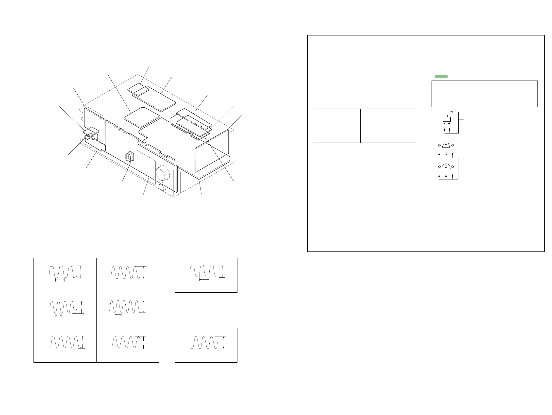
• Waveforms (DIGITAL Board)
1V/DIV 50nsec/DIV
1
IC1301
1V/DIV 20nsec/DIV
2
1V/DIV 50nsec/DIV
3
IC1501
80nsec
ws
24.576MHz
IC1306
13.59MHz
qs
3.6Vp-p
(XIN)
3.6Vp-p
2
3.2Vp-p
(MCLK2)
4
5
6
1V/DIV 50nsec/DIV
13.5MHz
IC1551
IC1551
<zc.
1V/DIV 20nsec/DIV
40nsec
0
1V/DIV 20nsec/DIV
16.5MHz
IC1101
3.2Vp-p
(MCLK2)
4.0Vp-p
(SCKOUT)
3.2Vp-p
(X1)
tj
• Waveform (DISPLAY Board)
1V/DIV 0.2µsec/DIV
1
3.5Vp-p
0.48µsec
IC101
• Waveform (VIDEO Board)
1V/DIV 20nsec/DIV
1
IC252
(CLK)
e;
14.31818MHz
(XS)
9
4.2Vp-p
21 21
STR-DE885/DE985
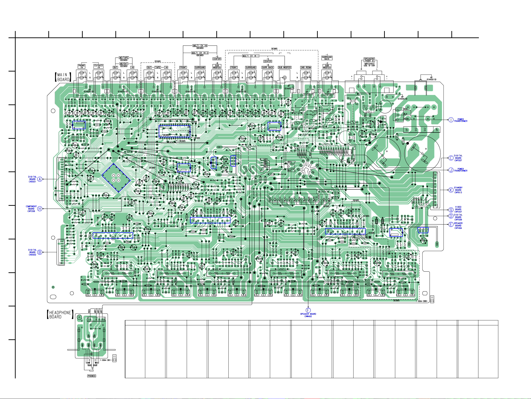
4-3. PRINTED WIRING BOARDS — MAIN SECTION — • Refer to page 21 for Circuit Boards Location and Common Note on Printed Wiring Boards.
A
B
C
D
E
F
G
H
1
(Page 27)
(Page 40)
(Page 27)
234567891011 12 13 14
J308
J309
R639
R333
RY351
96
R3
301
D
R835
CNP812
R481
R535
807
H
JW
R834
01
881
838
Q3
Q
R336
R
841
R839
840
JW
R337
JW
828
824
JW
JW
R431
C431
CN808
C481
JW849
C461
C466
139
JW
466
R
C463
751
D
806
H
JW
R475
Q474 Q473
JWH809
C464
09
1
110
R487
JW
JW
C471
76
R4
3
R471
47
JW
472
R474
R
Q472
882
Q
398
R
333
JW
R397
CNP813
825
JW
826
JW
C411
461
R
108
JW
76
4
Q
462
R
R465
C465
R478
471
Q
843
R
351
D
D882
Q351
CNP802
827
JW
462
C
IC400
480
R
R473
842
R
29
8
JW
813
JW
C416
484
R
830
JW
833
JW
R411
477
Q
C473
RY882
R882
L884
JWH803
C412
R415
C415
496
R
76
475
D
C4
TM603
BT800
JW881
883
R
CN881
802
D
6
81
4
C805
JW
88
R
D803
JW839
JW850
0
847
848
811
81
JW
JW
JW
JW
JWH802
812
JW
205
204
206
JW
JW
JW
3
412
400
C41
R
R
R416
JW203
C414
C477
486
483
R
JW472
C424
79
R4
C475
R477
485
R
R
9
42
JW
R425
476
D
88
R4
Q475
C807
814
JW
742
R
806
C
JW140
Q424
L883
801
P
CN
801
Q
R804
803
R
L801
JW
H
801
38
R7
732
R
105
104
JW
JW
103
JW
C421
836
835
802
JW
JW
R
801
C
C
8
0
4
JW815
CNP815
5
736
Q724
R
IC730
731
JW
446
R
421
R
426
D
438
R
R428
R73
737
731
R
R
7
4
42
Q
R43
5
433
426
C
R
D42
R423
421
Q
C423
739
R
733
731
R
C
437
R
30
R4
426
Q
22
102
R4
JW
R424
Q422
Q423
802
C
C427
429
R
JW801
JW802
D801
C803
804
805
JW
JW
803
NP
807
806
C
JW
JW
JW803
6
735
723
D
D73
Q
733
IC813
JW
4
73
R
Q425
JW471
C815
C816
6
435
R
R43
427
425
R
C
426
R
474
JW
C459
CNP811
CNP810
353
R
JW464
JW465
356
R
354
R
464
R
C353
R459
R460
C309
357
R
R467
401
JW
428
JW
667
JW
JW467
C497
C498
C499
R743
R745
R744
R351
357
C
458
R
R457
R463
R455
352
R
C358
C460
R454
453
R
652
Q
R656
R659
517
JW
C355
C354
468
R
C352
IC301
JW422
JW421
JW430
427
JW
R658
R452
JW486
R443
R772
500
R
633
R
C623
401
R
C491
834
JW
636
R
629
R
D881
635
R
815
H
JW
561
JW
626
D
R402
RY881
841
R
741
R
H814
JW
R627
J304
551
R
C174
625
Q
C625
R552
485
JW
H813
JW
C581
H812
JW
581
R
C521
501
R
184
R
499
JW
C124
R525
C681
811
H
JW
806
CN
681
R
C524
502
R
R183
651
R
C184
C631
R631
R753
810
H
JW
116
JW
J302
J301
612
R
676
D
JW426
R470
C428
C611
C612
679
R
314
R
C364
C429
C742
R317
JW441
JW443
611
R
R600
675
Q
516
JW
C394
C613
R616
131
JW
364
R
367
R
JW440
C479
498
JW
615
R
677
R
676
R
403
JW
C615
R686
C675
C310
418
JW
JWH822
C420
C666
603
JW
C664
D675
C676
132
JW
311
R
R362
Q677
672
R
R674
Q672
C311
R308
R309
C661
666
R
661
R
IC600
682
R
671
R
C308
JW417
662
C
696
R
313
R
312
R
JWH820
C422
662
R
687
R
Q676
R678
671
Q
466
JW
IC
C741
680
R
673
R
C314
JW468
JW402
4
0
1
683
R
C673
JWB801
Q673
R363
JW469
475
JW
C614
302
301
302
C356
R359
415
JW
C419
771
Q
R
C305
C303
C360
721
R
R675
C674
355
R
434
JW
JW604
R771
Q721
R361
R
C
303
C304
C361
304
R
R
R305
C306
C359
423
JW
307
306
R
R
C307
358
R
JW419
JW420
JW411
JW416
C418
424
C417
JW
C478
432
433
JW
JW
437
436
435
441
R
722
Q
C671
JW
JW
JW
605
JW
C663
JW518
JW601
JW602
C677
684
C665
R
R665
JW164
JWB802
Q674 Q524 Q523
470
JW
JW408
JW438
JW504
497
JW
685
R
404
JW
C438
490
JW
C616
479
JW
C571
R315
JW405
JW406
JW407
JW410
JW439
JW446
JW
JW501
JW502
R395
JW503
C694
480
JW
129
JW
R575
Q574
H821
JW506
695
R
481
JW
128
JW
C575
365
R
R318
JWH823
C494
JW505
JW507
691
Q
127
JW
J303
C316
JW458
C430
C432
JW508
482
JW
130
JW
JW409
JWH817
CNP814
440
R
478
JW
316
R
JW459
JW
509
JW
R694
572
R
R574
Q572
H
C595
R587
C366
R368
JW462
818
469
R
C643
126
JW
R571
366
R
JW457
JW460
514
JW
510
JW
693
R
C693
R644
580
R
Q576
R578
571
Q
320
R
C490
515
JW
511
JW
Q641
C319
R643
579
R
573
R
IC402
491
R
512
JW
R584
R645
576
D
583
R
Q573
513
JW
JW118
C573
319
R
C369
JW456
JW461
JWH816
R490
IC604
C495
C544
C594
477
476
JW
JW
596
R
588
C576
R
370
R
R495
C467
Q577
R369
JWH819
483
JW
C577
D575
C444
R595
C468
C564
575
Q
C390
C321
448
JW
R444
577
R
R576
323
372
R
C323
454
JW
IC812
JW860
R394
C543
Q541
562
R
119
JW
R
R543
C562
R626
C511C561
637
R
Q626
373
R451
R
374
R
324
R
C373
C451
455
JW463
JW
C811
C813
447
IC811
JW
C812
C814
D811
JW487
R445
Q391
C443
Q441
C393
R393
R494
493
Q491
R544
R
C493
JW484
C516C566
516
R
511
R
512
C513
C512
R
JW525
JW526
C721
JW527
C514
515
C515
R
C627
627
646
Q
R
R630
634
632
D625
R
R
C626
R628
621
R623
R
Q621
R622
R624
Q622
Q623
R371
R321
322
R
C371
452
JW
453
450
451
JW
JW
JW
449
JW846
JW
311
312
JW
JW
391
392
R
R
R390
C391
C395
R545
R593
C593
489
R594
JW
Q591
561
R
566
C563
R
IC500
JW528
C565
R565
121
120
JW
JW
586
R
R585
C578
C621
R625
JW117
C624
Q624
134
R
652
R
C531
822
JW
C752
752
R
C601C651C501C551C401
IC103
R133
115
JW
521
JW
C134
114
JW
R601
R840
752
Q
844
JW
537
R
526
Q
C123
113
JW
R524
Q522
R602
C173
JW842
R881
854
JW
JW852
C751
112
JW
530
R
522
R
R654
R531
D752
538
R
R526
521
R
J305
853
JW
JW823
JW821
R546
C526
R528
521
Q
C654
132
R
527
Q
534
R
182
R181
R
131
R
843
JW
130
Q
845
JW
CNP882
JWH804
JW851
R754
D753
R750
D526
525
D
523
R
C523
RY130
D130
136
R
CN807
C527
533
R
JW520
J103
RY601
R135
R638
R137
JW138
GP1
157
156
JW
JW
R751
3
75
751
Q
Q
560
JW
808
H
R536
JW
525
529
C525
Q
R
R527
C474
(Page 42)
(Page 27)
(Page 42)
(Page 42)
(Page 36)
(Page 27)
(Page 32)
• Semiconductor Location
I
TP700
CNP701
C702
J
J701
Ref. No. Location Ref. No. Location Ref. No. Location Ref. No. Location Ref. No. Location
(D130) C-9
D301 C-10
D351 C-10
(D425) G-12
(D426) G-12
D475 G-10
D476 G-11
D525 G-9
D526 G-9
D575 G-6
D576 G-5
D625 G-7
D626 G-7
D675 G-3
D676 G-4
D735 F-12
D736 F-12
D751 F-9
D752 F-8
D753 F-9
D801 C-13
D802 C-11
D803 D-11
D811 E-7
D881 D-7
D882 C-10
(IC103) C-8
IC301 C-2
IC400 F-10
IC401 E-4
(IC402) C-5
IC500 F-6
IC600 F-3
IC604 D-6
IC730 F-12
IC811 D-7
IC812 D-6
IC813 F-13
(Q130) D-9
Q301 C-10
Q351 C-10
Q391 E-7
(Q421) H-12
(Q422) H-12
(Q423) H-12
(Q424) H-11
(Q425) G-12
(Q426) G-12
(Q427) G-12
Q441 E-7
Q471 H-10
Q472 H-10
Q473 H-10
Q474 H-10
Q475 G-11
Q476 G-10
Q477 G-10
Q491 E-7
(Page 32)
Ref. No. Location Ref. No. Location
Q521 H-8
Q522 H-8
Q523 H-9
Q524 H-8
Q525 G-9
Q526 G-8
Q527 G-9
Q541 E-6
Q571 H-5
Q572 H-5
Q573 H-5
Q574 H-5
Q575 G-6
Q576 G-5
Q577 G-6
Q591 E-6
Q621 H-7
Q622 H-7
Q623 H-7
Q624 H-6
Q625 G-7
Q626 G-7
Q627 G-7
Q641 F-5
Ref. No. Location
Q652 F-2
Q671 H-3
Q672 H-3
Q673 H-4
Q674 H-3
Q675 G-4
Q676 G-4
Q677 G-3
Q691 F-5
Q721 F-3
Q722 G-3
Q723 F-12
Ref. No. Location
Q724 F-12
Q751 F-9
Q752 F-8
Q753 F-9
Q771 F-2
Q801 C-12
Q881 C-10
Q882 C-10
( ) : STR-DE985 only
2222
 Loading...