

Page 1
2019/03/1322:12:27(GMT+09:00)
MHC-V82D
SERVICE MANUAL
Ver. 1.0 2019.02
Note:
Be sure to keep your PC used for service and
checking of this unit always updated with the
latest version of your anti-virus software.
In case a virus aff ected unit was found during
service, contact your Service Headquarters.
AEP Model
E Model
Model Name Using Similar Mechanism MHC-V81D
DVD Mechanism Type CDM90-DVBU204//M
Optical Pick-up Name CMS-S76RFS7GP
Speaker section
Speaker system:
5-way, Double Bass Refl ex
Speaker unit:
Tweeter L/R Front: 50 mm, cone type
Tweeter L/R Rear: 50 mm, cone type
Midrange L/R (Upper): 100 mm,
cone type
Midrange L/R (Lower): 120 mm,
cone type
Woofer: 300 mm, cone type
Inputs
AUDIO/PARTY CHAIN IN (TV) L/R:
Voltage 2 V, impedance 24 kilohms
TV (ARC):
Supported audio signal:
2-channel Linear PCM
MIC1:
Sensitivity 1 mV, impedance 10 kilohms
MIC2/GUITAR:
Sensitivity 1 mV, impedance 10 kilohms
(When guitar mode is turned off .)
Sensitivity 200 mV, impedance
250 kilohms (When guitar mode is
turned on.)
Outputs
AUDIO/PARTY CHAIN OUT L/R:
Voltage 2 V, impedance 1 kilohm
HDMI OUT (TV) ARC:
Supported audio signal:
2-channel Linear PCM (up to 48 kHz),
Dolby Digital
HDMI section
Connector:
Type A (19 pin)
Disc player section
System:
Compact disc and digital audio and
video system
SPECIFICATIONS
Laser Diode Properties
Emission Duration: Continuous
Laser Output*: Less than 44.6 μW
* This output is the value measurement
at a distance of 200 mm from the
objective lens surface on the Optical
Pick-up Block with 7 mm aperture.
Frequency response:
20 Hz – 20 kHz
Video color system format:
Latin American models:
NTSC
Other models:
NTSC and PAL
USB section
Supported USB device:
Mass Storage Class
Maximum current:
1 A
(USB) port:
Type A
FM tuner section
FM stereo, FM superheterodyne tuner
Antenna:
FM lead antenna
Tuning range:
87.5 MHz – 108.0 MHz (50 kHz step)
BLUETOOTH section
Communication system:
BLUETOOTH Standard version 4.2
Output:
BLUETOOTH Standard Power Class 2
Maximum output power:
<9.5 dBm
Maximum number of devices to be
registered:
8 devices
Maximum number of simultaneous
connection (Multipoint):
3 devices
Maximum communication range:
Line of sight approx. 10 m
1)
Frequency band:
2.4 GHz band (2.4000 GHz –
2.4835 GHz)
Modulation method:
FHSS (Freq Hopping Spread Spectrum)
Compatible BLUETOOTH profiles2):
A2DP (Advanced Audio Distribution
Profile)
AVRCP (Audio Video Remote
Control Profile)
SPP (Serial Port Profile)
Supported codecs:
SBC (Subband Codec)
AAC (Advanced Audio Coding)
LDAC
1)
The actual range will vary depending on
factors such as obstacles between devices,
magnetic fields around a microwave oven,
static electricity, reception sensitivity,
antenna’s performance, operating system,
software application, etc.
2)
BLUETOOTH standard profiles
indicate the purpose of BLUETOOTH
communication between devices.
NFC section
Frequency band:
13.56 MHz
Supported audio formats
Supported bit rate and sampling frequencies:
MP3:
32/44.1/48 kHz, 32 kbps –
320 kbps (VBR)
AAC:
44.1 kHz, 48 kbps – 320 kbps
(CBR/VBR)
WMA:
44.1 kHz, 48 kbps – 192 kbps
(CBR/VBR)
WAV:
44.1/48 kHz (16 bit)
Supported video formats
Xvid:
Video codec: Xvid video
Bit rate: 4.854 Mbps (MAX)
Resolution/Frame rate:
720 × 480, 30 fps
720 × 576, 25 fps (except for Latin
American models)
Audio codec: MP3
MPEG4:
File format: MP4 File Format
Video codec: MPEG4 Simple
Profile (AVC is not compatible.)
Bit rate: 4 Mbps
Resolution/Frame rate:
720 × 480, 30 fps
720 × 576, 25 fps (except for Latin
American models)
Audio codec: AAC-LC (HE-AAC is
not compatible.)
DRM: Not compatible
General
Power requirements:
AC 120 V – 240 V, 50/60 Hz
Power consumption:
190 W
Power consumption (at the Power Saving
mode):
0.5 W (When “BT STBY” is set
to “OFF” and [CONTROL FOR
HDMI] is set to [OFF].)
2 W* (When “BT STBY” is set to
“ON” and [CONTROL FOR HDMI]
is set to [ON].)
Dimensions (W/H/D) (Approx.):
370 mm × 1,060 mm × 427 mm
Mass (Approx.):
26.0 kg
Operating temperature:
5 °C to 35 °C
– Continued on next page –
9-930-600-01
2019B80-1
2019.02
©
HOME AUDIO SYSTEM
Sony Corporation
Published by Sony EMCS (Malaysia) PG Tec
SYSSET
Page 2
2019/03/1322:12:27(GMT+09:00)
MHC-V82D
* The power consumption of the system
will be less than 0.5 W when there is no
HDMI connection and “BT STBY” is set
to “OFF”.
Unpacking
•
This unit (MHC-V82D) (1)
•
Remote control (DC 3 V) (1)
• R03 (DC 1.5 V) (size AAA) batteries (2)
• FM lead antenna (aerial) (1)
• AC power cord (mains lead) (1)
• AC plug adaptor* (1) (supplied only for
certain areas)
* This plug adaptor is not for the use in
Chile, Paraguay and Uruguay. Use this
plug adaptor in the countries/regions where
it is necessary.
Design and specifications are subject to
change without notice.
License and Trademark Notice
•
is a trademark of DVD Format/Logo
Licensing Corporation.
•
“DVD+RW”, “DVD-RW”, “DVD+R”,
“DVD-R”,
“DVD VIDEO”, and the “CD”
logos are trademarks.
• WALKMAN® and WALKMAN® logo are
registered trademarks of Sony Corporation.
• MPEG Layer-3 audio coding technology
and patents licensed from Fraunhofer IIS
and Thomson.
• Windows Media is either a registered
trademark or trademark of Microsoft
Corporation in the United States and/or
other countries.
• This product is protected by certain
intellectual property rights of Microsoft
Corporation. Use or distribution of
such technology outside of this product
is prohibited without a license from
Microsoft or an authorized Microsoft
subsidiary.
• This system incorporates Dolby* Digital.
* Manufactured under license from Dolby
Laboratories. Dolby, Dolby Audio, and the
double-D symbol are trademarks of Dolby
Laboratories.
• This system incorporates HighDefinition Multimedia Interface
(HDMI™) technology. The terms HDMI
and HDMI High-Definition Multimedia
Interface, and the HDMI Logo are
trademarks or registered trademarks of
HDMI Licensing Administrator, Inc. in
the United States and other countries.
• “BRAVIA” is a trademark of Sony
Corporation.
• LDAC™ and LDAC logo are trademarks
of Sony Corporation.
• The BLUETOOTH
logos are registered trademarks owned
by the Bluetooth SIG, Inc. and any use
of such marks by Sony Corporation is
under license. Other trademarks and
trade names are those of their respective
owners.
• The N-Mark is a trademark or registered
trademark of NFC Forum, Inc. in the United
States and in other countries.
• Android, Google Play, and the Google
Play logo are trademarks of Google LLC.
• Apple, the Apple logo, iPhone, iPod,
and iPod touch are trademarks of Apple
Inc., registered in the U.S. and other
countries. App Store is a service mark
of Apple Inc., registered in the U.S. and
other countries.
• Use of the Made for Apple badge means
that an accessory has been designed
to connect specifically to the Apple
product(s) identified in the badge, and
has been certified by the developer to
meet Apple performance standards. Apple
is not responsible for the operation of this
device or its compliance with safety and
regulatory standards.
®
word mark and
• THIS PRODUCT IS LICENSED UNDER
THE MPEG-4 VISUAL PATENT
PORTFOLIO LICENSE FOR THE
PERSONAL AND NON-COMMERCIAL
USE OF A CONSUMER FOR
(i) ENCODING VIDEO IN COMPLIANCE
WITH THE MPEG-4 VISUAL STAN-
DARD (“MPEG-4 VIDEO”)
AND/OR
(ii)
DECODING MPEG-4 VIDEO THAT
WAS ENCODED BY A CONSUMER
ENGAGED IN A PERSONAL AND
NON-COMMERCIAL ACTIVITY AND/
OR WAS OBTAINED FROM A VIDEO
PROVIDER LICENSED TO PROVIDE
MPEG-4 VIDEO.
NO LICENSE IS GRANTED OR SHALL
BE IMPLIED FOR ANY OTHER USE. ADDITIONAL INFORMATION INCLUDING
THAT RELATING TO PROMOTIONAL,
INTERNAL AND COMMERCIAL USES
AND LICENSING MAY BE OBTAINED
FROM MPEG LA, L.L.C.
HTTP://WWW.MPEGLA.COM
• All other trademarks are trademarks of
their respective owners.
• In this manual, ™ and
specified.
®
marks are not
NOTES ON CHIP COMPONENT REPLACEMENT
• Never reuse a disconnected chip component.
• Notice that the minus side of a tantalum capacitor may be damaged by heat.
FLEXIBLE CIRCUIT BOARD REPAIRING
• Keep the temperature of the soldering iron around 270 °C during repairing.
• Do not touch the soldering iron on the same conductor of the
circuit board (within 3 times).
• Be careful not to apply force on the conductor when soldering
or unsoldering.
SAFETY CHECK-OUT
After correcting the original service problem, perform the following
safety check before releasing the set to the customer:
Check the antenna terminals, metal trim, “metallized” knobs,
screws, and all other exposed metal parts for AC leakage. Check
leakage as described below.
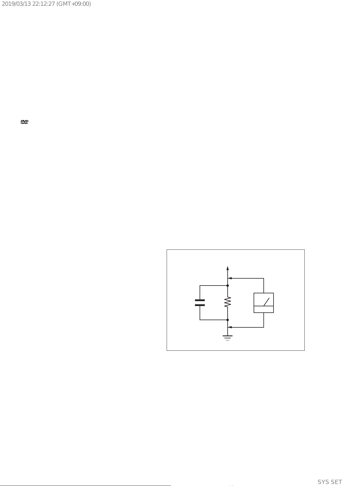
LEAKAGE TEST
The AC leakage from any exposed metal part to earth ground and
from all exposed metal parts to any exposed metal part having a
return to chassis, must not exceed 0.5 mA (500 microamperes).
Leakage current can be measured by any one of three methods.
1. A commercial leakage tester, such as the Simpson 229 or RCA
WT-540A. Follow the manufacturers’ instructions to use these
instruments.
2. A battery-operated AC milliammeter. The Data Precision 245
digital multimeter is suitable for this job.
3. Measuring the voltage drop across a resistor by means of a
VOM or battery-operated AC voltmeter. The “limit” indication
is 0.75 V, so analog meters must have an accurate low-voltage
scale. The Simpson 250 and Sanwa SH-63Trd are examples
of a passive VOM that is suitable. Nearly all battery operated
digital multimeters that have a 2V AC range are suitable. (See
Fig. A)
To Exposed Metal
Parts on Set
AC
1.5 kΩ0.15 μF
voltmeter
(0.75 V)
Earth Ground
Fig. A. Using an AC voltmeter to check AC leakage.
SAFETY-RELATED COMPONENT WARNING!
COMPONENTS IDENTIFIED BY MARK 0 OR DOTTED LINE
WITH MARK 0 ON THE SCHEMATIC DIAGRAMS AND IN
THE PARTS LIST ARE CRITICAL TO SAFE OPERATION.
REPLACE THESE COMPONENTS WITH SONY PARTS
WHOSE PART NUMBERS APPEAR AS SHOWN IN THIS
MANUAL OR IN SUPPLEMENTS PUBLISHED BY SONY.
2
SYSSET
Page 3
2019/03/1322:12:27(GMT+09:00)
MHC-V82D
TABLE OF CONTENTS
1. SERVICING NOTES ............................................. 4
2. DISASSEMBLY
2-1. Disassembly Flow ........................................................... 10
2-2. Side panel L, R ................................................................ 11
2-3. Loading Panel Assy ........................................................ 11
2-4. Vicente Top Panel Section .............................................. 12
2-5. Rear Cover ...................................................................... 13
2-6. CDM Section .................................................................. 14
2-7. CDM90-DVBU204//M ................................................... 15
2-8. Service, Optical Device (7G), Flexible Flat Cable ......... 16
2-9. SMPS Board (EMC) ....................................................... 17
2-10. MOTHERBOARD Board, Chassis Section .................... 18
2-11. Front Panel (Vicente) Section ......................................... 19
2-12. Bottom Cover Section ..................................................... 20
2-13. Loudspeaker (30cm) (Woofer) (SP9) .............................. 21
2-14. Loudspeaker (10cm) (Mid Top: L-CH) (SP2),
Loudspeaker (10cm) (Mid Top: R-CH) (SP6) ................ 22
2-15. Loudspeaker (12cm) (Mid Bottom: L-CH) (SP1),
Loudspeaker (12cm) (Mid Bottom: R-CH) (SP5) .......... 23
3. TEST MODE ............................................................ 24
4. ELECTRICAL CHECK ......................................... 25
5. TROUBLESHOOTING .......................................... 26
6. DIAGRAMS
6-1. Block Diagram
- RS SERVO, USB, TOUCH, HDMI Section - .............. 33
6-2. Block Diagram - MAIN Section - ................................... 34
6-3. Block Diagram - AMP Section - ..................................... 35
6-4. Block Diagram
- PANEL, POWER SUPPLY Section - ........................... 36
6-5. Block Diagram - SMPS Section - ................................... 37
6-6. Printed Wiring Board - MOTHERBOARD Board
(Component Side) - ......................................................... 39
6-7. Printed Wiring Board - MOTHERBOARD Board
(Conductor Side) - .......................................................... 40
6-8. Printed Wiring Board
- SENSOR Board (Component Side) - ........................... 41
6-9. Printed Wiring Board
- SENSOR Board (Conductor Side) - ............................. 42
6-10. Printed Wiring Board - SMPS Board (EMC) - ............... 43
6-11. Printed Wiring Board - VFD Board - .............................. 44
6-12. Printed Wiring Board - MIC USB Board - ..................... 45
6-13. Printed Wiring Board - POWER KEY Board -............... 46
6-14. Printed Wiring Board - HUB Board - ............................. 46
6-15. Printed Wiring Board - 360 FR L Board - ...................... 47
6-16. Printed Wiring Board - 360 FR R Board - ...................... 47
6-17. Printed Wiring Board - 360 BACK L Board - ................ 48
6-18. Printed Wiring Board - 360 BACK R Board - ................ 48
6-19. Printed Wiring Board - SPK MID BTM Board - ............ 49
6-20. Printed Wiring Board - NFC Board - .............................. 49
6-21. Printed Wiring Board - EXTENSION Board - ............... 49
6-22. Printed Wiring Board - IR Board - .................................. 49
6-23. Printed Wiring Board - SPK MID L Board - .................. 50
6-24. Printed Wiring Board - SPK MID R Board - .................. 50
6-25. Printed Wiring Board - SW LED L Board - .................... 50
6-26. Printed Wiring Board - SW LED R Board - ................... 50
7. EXPLODED VIEWS
7-1. Side Panel Section .......................................................... 51
7-2. Panel Loading Section .................................................... 52
7-3. Rear Cover Section ......................................................... 53
7-4. SMPS Board (EMC) Section .......................................... 54
7-5. Chassis Section ............................................................... 55
7-6. Front Panel (Vicente) Section ......................................... 56
7-7. Bottom Cover Section ..................................................... 57
7-8. Loudspeaker Section ....................................................... 58
7-9. Speaker Cabinet Section ................................................. 59
7-10. Vicente Top Panel Section .............................................. 60
7-11. CDM Section .................................................................. 61
7-12. DVD Mechanism Section (CDM90-DVBU204//M) ...... 62
8. ELECTRICAL PARTS LIST .............................. 63
Accessories are listed in the last part of the electrical parts list.
3
SYSSET
Page 4
2019/03/1322:12:27(GMT+09:00)
MHC-V82D
SECTION 1
SECTION 1
SERVICING NOTES
SERVICING NOTES
UNLEADED SOLDER
Boards requiring use of unleaded solder are printed with the
leadfree mark (LF) indicating the solder contains no lead.
(Caution: Some printed circuit boards may not come printed with
the lead free mark due to their particular size)
: LEAD FREE MARK
Unleaded solder has the following characteristics.
• Unleaded solder melts at a temperature about 40 °C higher
than ordinary solder.
Ordinary soldering irons can be used but the iron tip has to be
applied to the solder joint for a slightly longer time.
Soldering irons using a temperature regulator should be set to
about 350 °C.
Caution: The printed pattern (copper foil) may peel away if
the heated tip is applied for too long, so be careful!
• Strong viscosity
Unleaded solder is more viscous (sticky, less prone to fl ow)
than ordinary solder so use caution not to let solder bridges
occur such as on IC pins, etc.
• Usable with ordinary solder
It is best to use only unleaded solder but unleaded solder may
also be added to ordinary solder.
CAUTION
Use of controls or adjustments or performance of procedures
other than those specifi ed herein may result in hazardous radiation
exposure.
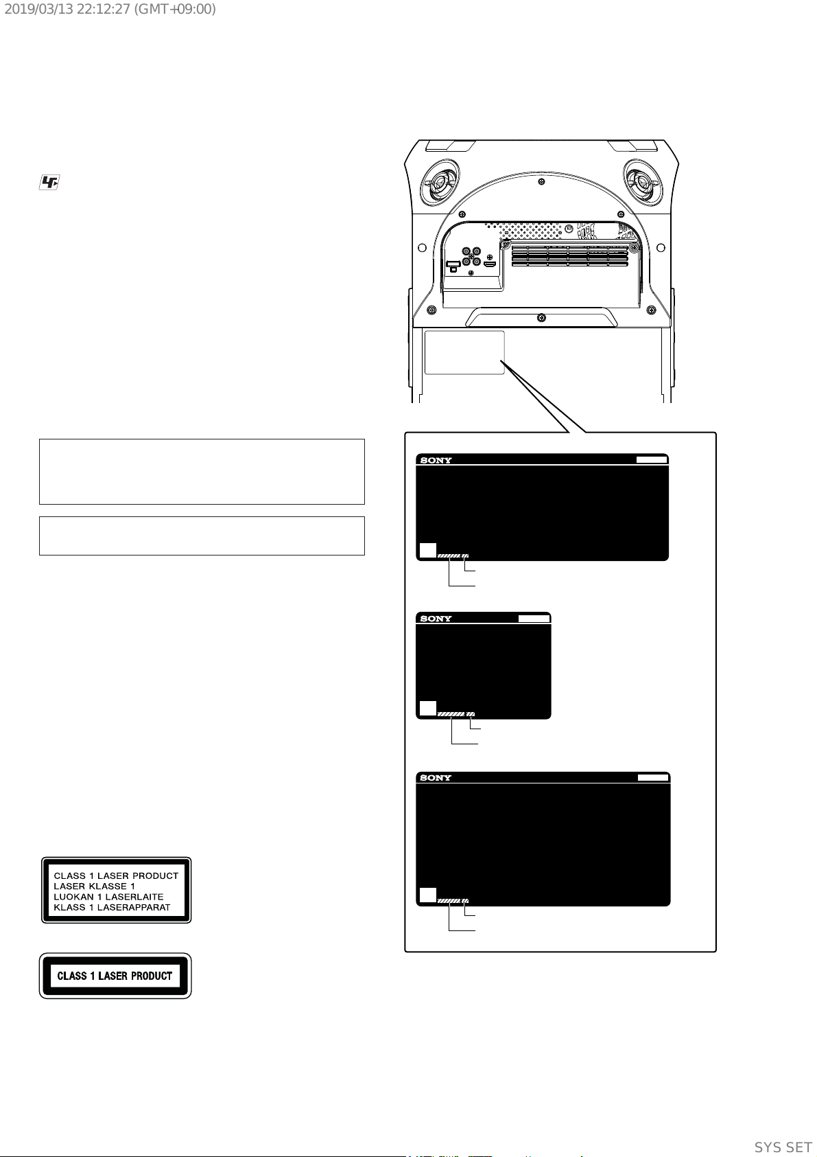
MODEL IDENTIFICATION
– Rear view –
MODEL NUMBER LABEL
AEP, RU, LA9, AR, MY, EA
R
MODEL NO. :
MHC-V82D
NOTES ON HANDLING THE OPTICAL PICK-UP BLOCK
OR BASE UNIT
The laser diode in the optical pick-up block may suff er electrostatic
break-down because of the potential diff erence generated by the
charged electrostatic load, etc. on clothing and the human body.
During repair, pay attention to electrostatic break-down and also
use the procedure in the printed matter which is included in the
repair parts.
The fl exible board is easily damaged and should be handled with
care.
NOTES ON LASER DIODE EMISSION CHECK
The laser beam on this model is concentrated so as to be focused
on the disc refl ective surface by the objective lens in the optical
pickup block. Therefore, when checking the laser diode emission,
observe from more than 30 cm away from the objective lens.
CAUTION
The use of optical instruments with this product will increase eye
hazard.
For customers in AEP
This appliance is classifi ed as a
CLASS 1 LASER product under
IEC 60825-1:2007 and IEC
60825-1:2014. This marking is
located on the rear exterior.
For customers in EA
This appliance is classifi ed as a
CLASS 1 LASER product under
IEC 60825-1:2007 and IEC
60825-1:2014. This marking is
located on the rear exterior.
CAUTION
Risk of explosion if the battery is replaced by an incorrect type.
E4, E12
TH
Destination Code
PART No.
R
MODEL NO. :
Destination Code
PART No.
R
Destination Code
PART No.
MHC-V82D
MODEL NO. :
MHC-V82D
Do not expose batteries or appliances with battery-installed to excessive heat, such as sunshine and fi re.
4
SYSSET
Page 5
2019/03/1322:12:27(GMT+09:00)
MHC-V82D
Model Part No.
LA9
AEP
E4
E12
EA
TH
RU
AR
MY
4-746-522-0[]
4-747-800-0[]
4-747-979-0[]
4-747-979-2[]
4-747-981-0[]
4-748-006-0[]
4-748-008-0[]
4-748-011-0[]
4-748-016-0[]
DESTINATION ABBREVIATIONS
The following abbreviations for model destinations are used in this
service manual.
• Abbreviation
AR : Argentina model
E4 : African model
E12 : 220-240 V AC area in E model
EA : Saudi Arabia model
LA9 : Latin-American model
MY : Malaysia model
RU : Russian model
TH : Thai model
DESTINATION SETTING METHOD
The destination information isn’t written in the MOTHERBOARD
board for the service.
Therefore, when the MOTHERBOARD board is replaced, be sure
to perform the destination setting (Important work).
Note 1: The initial setting destination of the MOTHERBOARD board for
the service is temporary set as “LATIN”. The message “DEST
ERR” is displayed on the screen display panel.
Note 2: When distinguishing the destination of the product, refer to the
“MODEL IDENTIFICATION” on page 4.
Note 3: If destination setting isn’t performed, it is possibility to occur the
defect to each operation of this unit.
Note 4: Destination would be locked if it has changed for 5 times.
Procedure:
1. Touch two touch keys of the [SOUND FIELD] and [TUNING
+ >] simultaneously for 5 seconds during the demo mode.
2. It enters the destination setting mode, the message
“D XXXXX” is displayed on the screen display panel.
Note 5: If the message “DESTLOCK” is displayed on the screen display
panel, touch the [N] touch key to release from this mode. Because the destination is locked, and it cannot change the destination.
3. Touch [ +] / [ ―] touch key to select the destination based
on the set’s country.
Screen
display
Destination
code
Country
“D ASIA” SP6, TH1 Southeast Asia countries
“D INDIA
“D ME AFC
” E12 India
” E3, E93, E4,
Middle East & Africa countries
SA2, EA3
“D OCEANI
” AU1 Australia & New Zealand
“D JAPAN” J1 Japan
“D BRAZIL” BR1 Brazil
“D N AME” UC2, CA2 America & Canada
“D LATIN” LA9, AR2 Central & South America
countries (except Brazil)
“D RUSSIA” RU1 Russia & CIS country
“D EUROPE
” CEL, CEK Europe countries
(except CIS country)
4. Touch [N] touch key to confi rm the selection.
5. “RESET” appears on the screen display panel. After that,
“SONY” appears on the screen display panel. The system
automatically turn on and off once. Please be sure that the
system stay at demo mode fi nally before switch off the power
supply.
6. Mode in “MODEL, DESTINATION AND VERSION
DISPLAY MODE” on page 24 again to confi rm on the model
& destination.
NOTE OF REPLACEMENT OF THE SENSOR BOARD
When the SENSOR board is defective, exchange the VICENTE
TOP PANEL ASSY SERVICE.
NOTE OF REPLACEMENT OF THE MS-476 BOARD
When the MS-476 board is defective, exchange the entire
LOADING COMPLETE ASSY (T).
TEST DISCS
Use following TEST DISC when this unit confi rms the operation
and checks it.
• For CD
Part No. Description
3-702-101-01 DISC (YEDS-18), TEST
4-225-203-01 DISC (PATD-012), TEST
J-2501-307-A DISC (HLX-A1), TEST
• For DVD SL (Single Layer)
Part No. Description
J-6090-069-A DISC (HLX-503), TEST (NTSC)
J-6090-088-A DISC (HLX-504), TEST (NTSC)
J-2501-305-A DISC (HLX-513), TEST (NTSC)
J-6090-077-A DISC (HLX-506), TEST (PAL)
• For DVD DL (Double Layer)
Part No. Description
J-6090-071-A DISC (HLX-501), TEST (NTSC)
J-6090-089-A DISC (HLX-505), TEST (NTSC)
J-2501-306-A DISC (HLX-514), TEST (NTSC)
J-6090-078-A DISC (HLX-507), TEST (PAL)
RELEASING THE DISC TRAY LOCK
The disc tray lock function for the antitheft of sample disc in the
shop is equipped.
It can release the lock function in the following procedure.
Releasing Procedure:
1. Press the [1] button to turn the power on.
2. Touch the [FUNCTION] touch key to select the DVD/CD
function.
3. Touch [MEGA BASS] touch key and [VOCAL FADER] touch
key simultaneously for three seconds.
4. The message “UNLOCKED” is displayed on the screen
display panel and the disc tray is unlocked.
Note: When “LOCKED” is displayed on the screen display panel, the
disc tray lock is not released by turning the power on/off with the
[1] button.
5
SYSSET
Page 6
2019/03/1322:12:27(GMT+09:00)
MHC-V82D
IF ERROR CODE AND “CHECK MANUAL” FLASHES
ON THE DISPLAY
See the following table for the corrective action.
Error code Corrective action
“PROTECT2” Contact your nearest Sony dealer.
“PROTECT3”/
“PROTECT4”/
“PROTECT6”
Protect Type Description:
X (Error Code) Description
2 Defect of thermistor IC or charging circuit
3 • There is possibility of over current hap-
4 or 6 • There is possibility of DC FAN is blocked
Immediately unplug the AC power cord
(mains lead), and check if anything is
blocking the ventilation openings of the
unit.
After you have checked and found no
problems, reconnect the AC power cord
(mains lead), and turn on the system.
If the issue persists, contact your nearest
Sony dealer.
used by SPM (Sound Pressure Management) system.
pen at speaker output or speaker damage
(shorted).
• Unusual heat up of AMP IC by improper
assembly of heatsink or lack of thermal
compound.
• Under voltage Protection (no supply to
AMP IC when power ON).
• DC appears in SP terminal by defect of
AMP IC.
or damaged.
• Defect of DC FAN driver circuit.
NOTE OF REPLACING THE IC2002 AND IC3503 ON
THE MOTHERBOARD BOARD AND THE MOTHERBOARD MOUNTED PC BOARD
When IC2002 and IC3503 on the MOTHERBOARD board
and the MOTHERBOARD mounted pc board are replaced, it is
necessary to spread the compound between parts and heat sink.
After that, execute “3. IC and MOTHERBOARD board after
replace checking guide” in page 31.
Spread the compound referring to the fi gure below.
– MOTHERBOARD Board (Component Side) –
compound
IC3503
IC2002
SELF-DIAGNOSIS FUNCTION
When the self-diagnosis function is activated, a service number
appears on the TV screen or the display.
The service number consists of an alphabet and numerals (e.g. C
13 50). See the following table for the cause and corrective action.
First 3 characters
of the service
number
C 13 This disc is dirty.
C 31 The disc is not inserted correctly.
E XX
(XX is a number)
Cause and corrective action
• Clean the disc with a soft cloth.
• Turn off the system, then turn it on
again.
Then re-insert the disc correctly.
To prevent a malfunction, the system has
performed the self-diagnosis function.
• Contact your nearest Sony dealer or
local authorized Sony service facility
and give the 5-character service
number.
Example: E 61 10
6
SYSSET
Page 7
2019/03/1322:12:27(GMT+09:00)
HOW TO OPEN THE TRAY WHEN POWER SWITCH TURN OFF
Note 1: After the side panel L, R are removed, this work is done.
Note 2: Please prepare the thin wire (clip etc. processed to the length of 5 cm or more).
1 Remove the side panel L, R.
(Illustration of disassembly is omitted.)
MHC-V82D
– Left view –
Insert the clip etc. processed to the
length of 5 cm or more in the hole
on the side of the CDM and push.
5 cm or more
Note: Push after it inserts it
in this hole well.
hole
DVD mechanism
deck
tray
– Top view –
3
2 Insert the clip etc.
7
SYSSET
Page 8
2019/03/1322:12:27(GMT+09:00)
MHC-V82D
CAPACITOR ELECTRICAL DISCHARGE PROCESSING
When removing the SMPS board (EMC) and MOTHERBOARD board, be sure to perform the discharge process by referring below
procedure.
Remove SMPS board (EMC) fi rst follow by MOTHERBOARD board.
Note: Be sure to discharge using a resistor of 500~800 .
SMPS Board (EMC) (Conductor Side view)
1. Disconnect all the wires and FFC which connected to the SMPS board (EMC) (avoid touching any component).
2. Unscrew the SMPS board (EMC).
3. Pulling up the wire (avoid touching any component) to lift up the SMPS board (EMC).
4. Flip the SMPS board (EMC) to conductor side and perform discharge at terminal of C6301, C6322, C6534, C6558 and C6559 for 10
seconds each.
800 :/5 W
800 :/5 W
800 :/5 W
R
800 :/5 W
R
R
C6559
C6558
C6534
R
C6301
800 :/5 W
R
C6322
MOTHERBOARD Board (Conductor Side view)
1. Disconnect all the wires and FFC which connected to the MOTHERBOARD board (avoid touching any component).
2. Unscrew the MOTHERBOARD board.
3. Holding the both edge (avoid touching any component) to lift up the MOTHERBOARD board.
4. Flip the MOTHERBOARD board to conductor side and perform discharge at terminal of C2133 and C3662 for 90 seconds each.
800 :/5 W
800 :/5 W
R
C2133
C3662
R
8
SYSSET
Page 9
2019/03/1322:12:27(GMT+09:00)
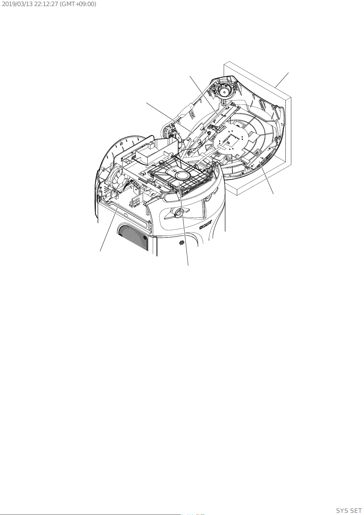
SERVICE POSITION
MHC-V82D
MIC US B board
VFD board
stand
POWER K E Y board
SMPS board (EMC)
CDM90-DVBU204//M
9
SYSSET
Page 10
2019/03/1322:12:27(GMT+09:00)
MHC-V82D
Note: Disassemble the unit in the order as shown below.
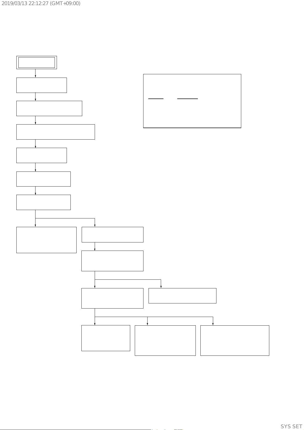
2-1. DISASSEMBLY FLOW
SET
2-2. SIDE PANEL L, R
(Page 11)
2-3. LOADING PANEL ASSY
(Page 11)
2-4. VICENTE TOP PANEL SECTION
(Page 12)
SECTION 2
DISASSEMBLY
JIG
When disassembling the unit, use the following
jig for speaker removal.
Part No. Description
J-2501-238-A JIG FOR SPEAKER REMOVAL
2-5. REAR COVER
(Page 13)
2-6. CDM SECTION
(Page 14)
2-7. CDM90-DVBU204//M
(Page 15)
2-8. SERVICE, OPTICAL
DEVICE (7G),
FLEXIBLE FLAT CABLE
(Page 16)
2-9. SMPS BOARD (EMC)
(Page 17)
2-10. MOTHERBOARD BOARD,
CHASSIS SECTION
(Page 18)
2-11. FRONT PANEL
(VICENTE) SECTION
(Page 19)
2-12. BOTTOM COVER SECTION
(Page 20)
10
2-13. LOUDSPEAKER
(30CM) (WOOFER)
(SP9)
(Page 21)
2-14. LOUDSPEAKER (10CM)
(MID TOP: L-CH) (SP2),
LOUDSPEAKER (10CM)
(MID TOP: R-CH) (SP6)
(Page 22)
2-15. LOUDSPEAKER (12CM)
(MID BOTTOM: L-CH) (SP1),
LOUDSPEAKER (12CM)
(MID BOTTOM: R-CH) (SP5)
(Page 23)
SYSSET
Page 11
2019/03/1322:12:27(GMT+09:00)
Note: Follow the disassembly procedure in the numerical order given.
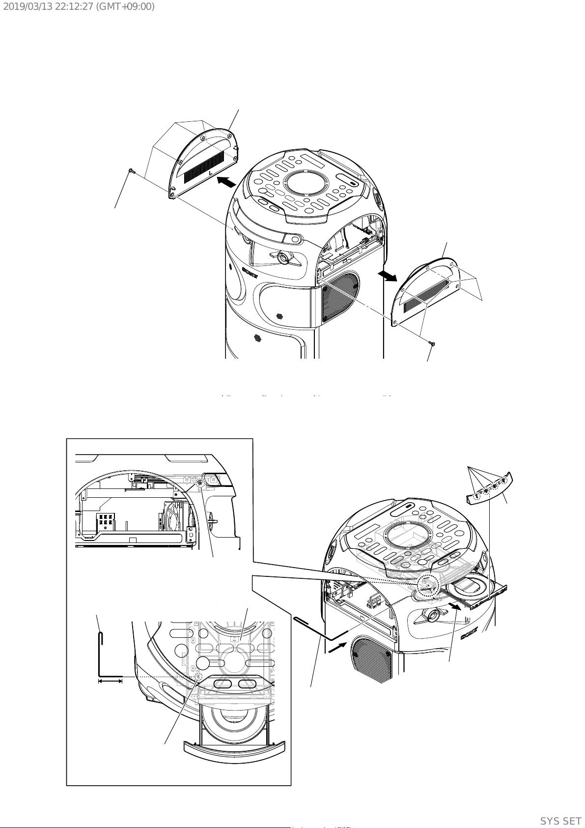
2-2. SIDE PANEL L, R
1 five screws
(tapping (flat head))
MHC-V82D
3 panel, side L
2
3 panel, side R
2
2-3. LOADING PANEL ASSY
– Left view –
Insert the clip etc. processed to the
length of 5 cm or more in the hole
on the side of the CDM and push.
1 five screws
(tapping (flat head))
3 four claws
4 panel, loading
assy
hole
DVD mechanism
deck
5 cm or more
Note: Push after it inserts it
in this hole well.
2 Draw out the tray.
1 Insert the clip etc.
tray
– Top view –
11
SYSSET
Page 12
2019/03/1322:12:27(GMT+09:00)
MHC-V82D
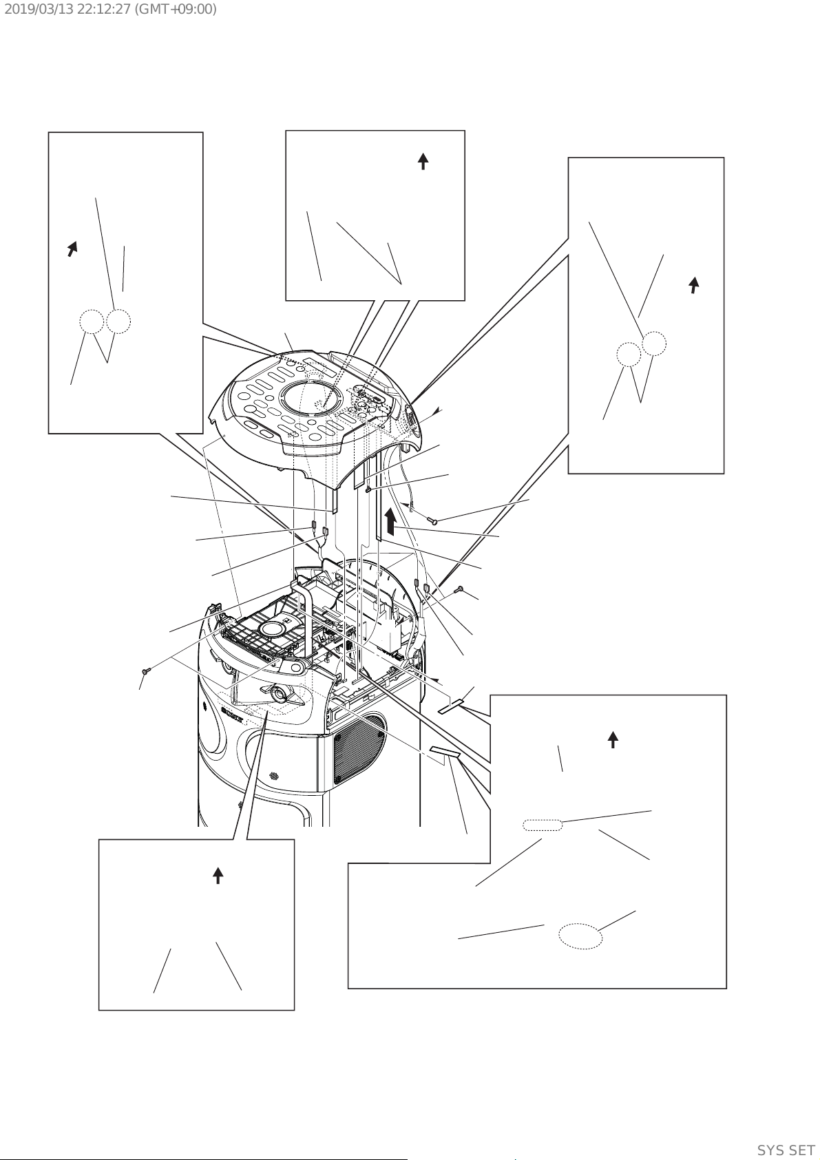
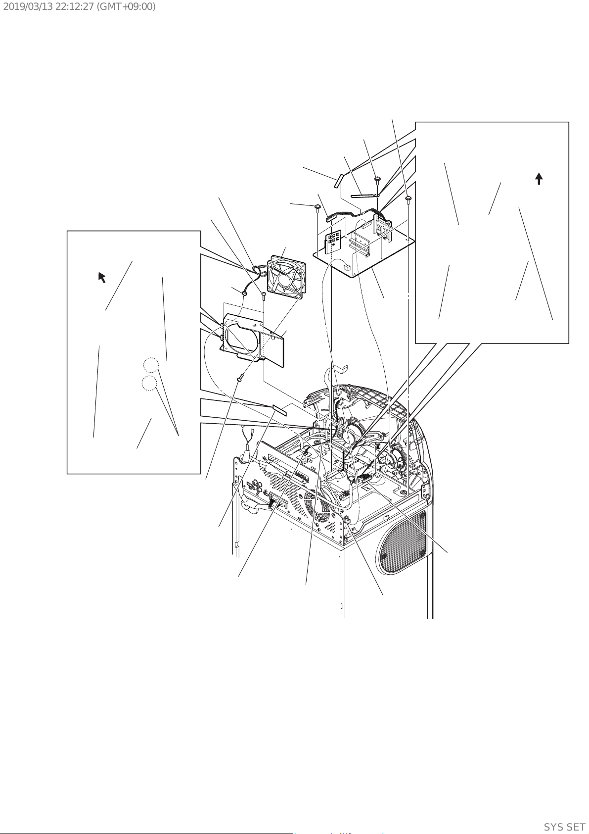
2-4. VICENTE TOP PANEL SECTION
:LUHVHWWLQJ
Push the protrusion, and
remove the terminal
(wide side) [grey].
loudspeaker (5cm)
top side
Push the protrusion,
and remove the terminal
(narrow side) [grey/black].
9 flexible flat cable
(17 core) (CN5001)
1 two screws
(tapping (flat head))
(tweeter) (L-CH)
(SP4)
protrusion
5 flexible flat cable
(7 core) (CN120)
qd terminal (narrow side)
[grey/black]
qd terminal (wide side)
[grey]
:LUHVHWWLQJ
qg VICENTE top panel
section
A
top side
filament tapeSENSOR board
B
A
4 flexible flat cable
(29 core) (CN126)
0 CN451 (5P)
3 one screw
(+BVTP 3 u 8) (SILVER)
qs Remove the VICENTE top panel
section in the direction of the arrow.
qa flexible flat cable
(9 core) (CN902)
2 three screws
(tapping (flat head))
qf terminal (wide side) [red]
qf terminal (narrow side) [red/black]
B
6 filament tape
:LUHVHWWLQJ
filament tape
:LUHVHWWLQJ
Push the protrusion, and
remove the terminal
(wide side) [red].
loudspeaker (5cm)
(tweeter) (R-CH) (SP8)
top side
protrusion
Push the protrusion, and
remove the terminal
(narrow side) [red/black].
top side
12
:LUHVHWWLQJ
filament tape
top side
HUB board
8 cushion (7T25), saranet
7 Draw out the flexible
flat cable (17 core)
from the hook.
cushion (7T25),
saranet
Note: Make sure the flexible flat cable (17 core)
must not near to the bluetooth module.
hook
bracket, CDM
bluetooth module
SYSSET
Page 13
2019/03/1322:12:27(GMT+09:00)
2-5. REAR COVER
MHC-V82D
6 three screws
(+BVTP 3 u 8) (BLACK)
7 cover, rear
2 cover, screw R
1 Insert the clip etc.
3 one screw
(+BVTP 3 u 8)
(BLACK)
4 two screws
(tapping
(flat head))
5 three screws
– Rear view –
(4 u 13) (TR-184A)
3 one screw
(+BVTP 3 u 8) (BLACK)
2 cover, screw L
1 Insert the clip etc.
13
SYSSET
Page 14
2019/03/1322:12:27(GMT+09:00)
MHC-V82D
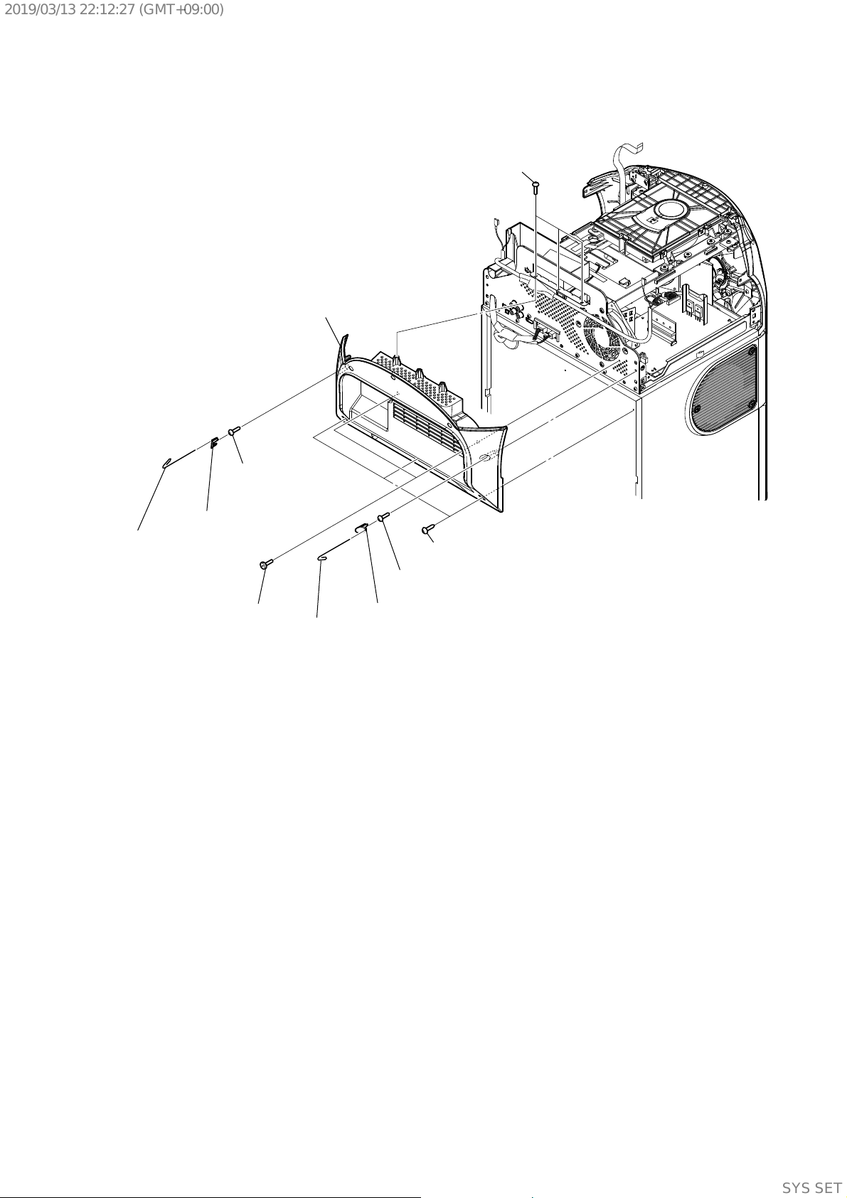
2-6. CDM SECTION
1 filament tape
:LUHVHWWLQJ
rear side
filament tape
CDM section
6 flexible flat cable
(24 core) (CN302)
7 two screws
(+BVTP 3 u 12)
hook
0 CDM section
3 CN2001 (2P)
9 Remove the CDM section
in the direction of the arrow.
5 flexible flat cable
(5 core) (CN303)
4 CN402 (4P)
8 two screws
(+BVTP 3 u 8)
(BLACK)
2 Remove wire from
the hook.
14
SYSSET
Page 15
2019/03/1322:12:27(GMT+09:00)
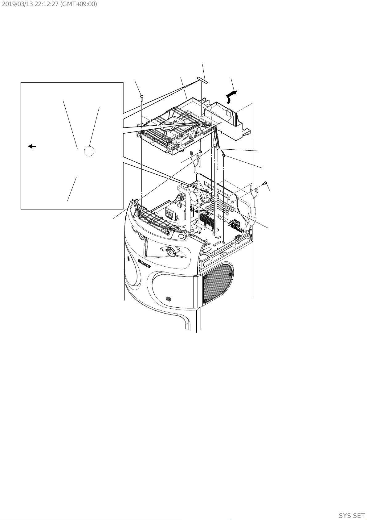
2-7. CDM90-DVBU204//M
:LUHVHWWLQJ
rear side
MHC-V82D
bracket, CDM
1 four screws
(+BVTP 3 u 8) (SILVER)
6 CDM90-DVBU204//M
5 Remove three wires from
the hook.
4 filament tape
CDM90-DVBU204//M
$(358($0<(
2 cushion, saranet
(30 u 50)
3 core, ferrite
hook
filament tape
7 bracket, CDM section
15
SYSSET
Page 16
2019/03/1322:12:27(GMT+09:00)
MHC-V82D
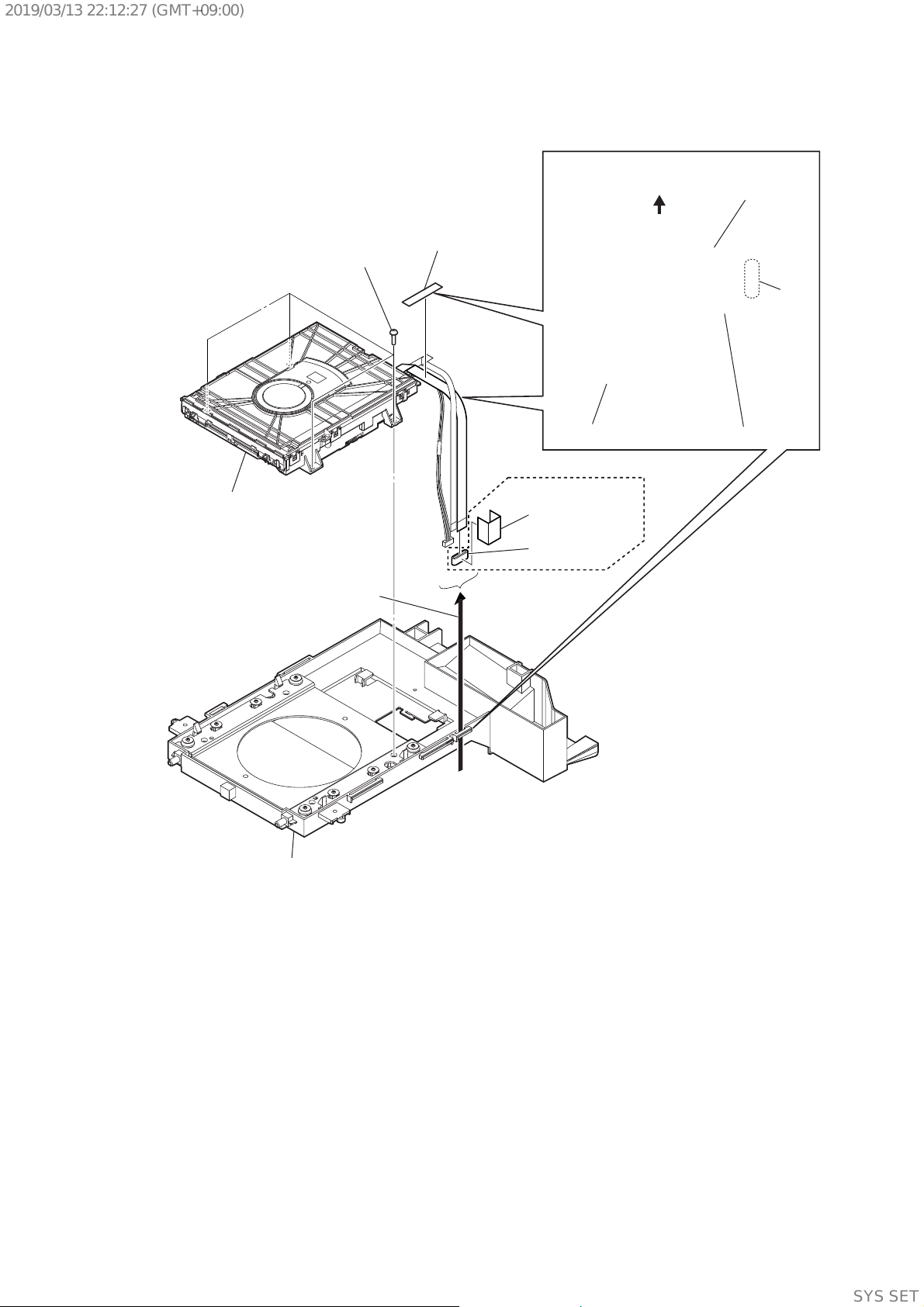
2-8. SERVICE, OPTICAL DEVICE (7G), FLEXIBLE FLAT CABLE
1 six claws
2 chuck holder assy (T)
qa insulator
7 four insulator screws
qg flexible flat cable
qs service, optical
device (7G)
qa insulator
6 belt
3 Insert the thin
wire (clip etc.).
qd base, lo assy
4
5 tray
,QVWDOODWLRQRIIOH[LEOHIODWFDEOHFRUHDQGIOH[LEOHIODWFDEOHFRUH
This illustration sees the loading assy (T) from bottom side.
Note:
5 two claws
1 flexible flat cable
loading assy (T)
(24 core)
3 Through the hole
8
0
9 connector
(5 core)
qa insulator
5 three claws
4
qf filament tape
qj holder, FFC
qk flexible flat cable
(24 core)
qh
loading assy (T)
– Bottom view –
6 holder, FFC
16
terminal face
2 Through the hole
Under the guide
(Fold area)
7 flexible flat cable
(24 core)
9 filament tape
8 flexible flat cable
(5 core)
Under the guide
SYSSET
Page 17
2019/03/1322:12:27(GMT+09:00)
2-9. SMPS BOARD (EMC)
6 two screws
(+BVTP 3 u 8) (SILVER)
:LUHVHWWLQJ
IR board
front side
1 Remove the wire
from the hook.
DC fan
2 CN2008
(3P)
qh three screws
(+PWH 3 u 8 (SUMITITE))
qh one screw
(+PWH 3 u 8 (SUMITITE))
0 cushion (CZ)
qs CN001 (11P)
qh two screws
(+PWH 3 u 8
(SUMITITE))
9 DC fan
qj clamp (N)
MHC-V82D
:LUHVHWWLQJ
qa Remove the
wire from clamp (N).
cushion (CZ)
front side
filament tape
MOTHERBOARD
board
hook
7 two screws
(+BVTP 3 u 8)
(SILVER)
4 filament
tape
5 CN127 (3P)
8 bracket,
fan
3 Remove the wire
from the hook.
qk SMPS
board
(EMC)
qg CN6000 (2P)
SMPS board (EMC)
MOTHERBOARD
board
qf CN6500 (8P)
qd Remove the wire
from clamp (N).
– Rear view –
17
SYSSET
Page 18
2019/03/1322:12:27(GMT+09:00)
MHC-V82D
2-10. MOTHERBOARD BOARD, CHASSIS SECTION
:LUHVHWWLQJ
rear side
MOTHERBOARD board
:LUHVHWWLQJ
loudspeaker
(5cm) (tweeter)
(L-CH) (SP3)
5 Remove the wire
from clamp (N).
Push the protrusion, and
remove the terminal
(wide side) [blue].
top side
9 one screw
(+PWH 3 u 8 (SUMITITE))
0 clamp (N)
9 one screw
(+PWH 3 u 8
(SUMITITE))
0 clamp
(N)
6 CN3501 (8P)
qk four step screws
M4
ql chassis
section
qs heat sink (MB-H)
Note 2: When you install the heat sink (MB-H), spread the compound
referring to “NOTE OF REPLACING THE IC2002 AND IC3503
ON THE MOTHERBOARD BOARD AND THE MOTHERBOARD
MOUNTED PC BOARD” on servicing notes (page 6).
9 six screws
(+PWH 3 u 8 (SUMITITE))
C
D
F
E
qd MOTHERBOARD
board
qa three screws
(+BVTP 3 u 8)
(SILVER)
8 one screw
(+B 3 u 6)
7 one screw
(+BVTP 3 u 8)
(BLACK)
C
D
F
E
qh six screws
(+BVTP 3 u 8)
(BLACK)
protrusion
Push the protrusion, and
remove the terminal
(narrow side) [blue/black].
:LUHVHWWLQJ
Push the protrusion, and
remove the terminal
(narrow side) [red/black].
loudspeaker
(5cm) (tweeter)
(R-CH) (SP7)
top
side
qf terminal
(wide side)
[blue]
qf terminal
(narrow side)
[blue/black]
qg terminal
(narrow side)
[red/black]
qj panel, back section
1 acoustic
tape
1 acoustic
tape
qg terminal
(wide side)
[red]
3 CN3502 (2P)
4 CN2005 (4P)
2 CN2206 (8P)
protrusion
Push the protrusion, and
remove the terminal
(wide side) [red].
18
Note 1: When the MOTHERBOARD mounted pc board
is replaced, be sure to refer to “DESTINATION
SETTING METHOD” on page 5.
SYSSET
Page 19
2019/03/1322:12:27(GMT+09:00)
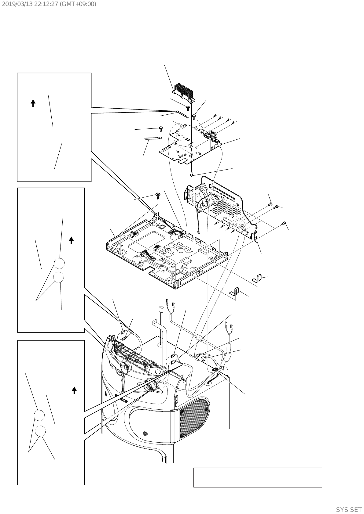
2-11. FRONT PANEL (VICENTE) SECTION
1 three screws
(+ flat tapping screw - ED BK)
6 All bosses are removed while moving
jig in the direction of the arrow, and
panel, front (VICENTE) section
is removed.
5 Insert the jig into a space and slowly
remove the panel, front (VICENTE) section.
Note 1: When using a jig, please work
so as not to injure panel, front
(VICENTE) section and
speaker cabinet.
3 sound generator
10CM
2
4 one screw
(4 u 13) (TR-184A)
4 one screw
(4 u 13) (TR-184A)
2
6 All bosses are removed while moving
jig in the direction of the arrow, and
panel, front (VICENTE) section is removed.
4 one screw
(4 u 13) (TR-184A)
MHC-V82D
3 sound generator 10CM
1 three screws
(+ flat tapping screw - ED BK)
5 Insert the jig into a space and
slowly remove the panel, front
(VICENTE) section.
Note 1: When using a jig, please work
so as not to injure panel, front
(VICENTE) section and
speaker cabinet.
5 Insert the jig into a space and slowly
remove the panel, front (VICENTE) section.
Note 1: When using a jig, please work
so as not to injure panel, front
(VICENTE) section and
speaker cabinet.
8 panel, front
(VICENTE) section
Note 2: When installing the panel, front
(VICENTE) section, remove the
used glue and use a new glue to
fix the panel, front (VICENTE).
7 Remove the
panel, front (VICENTE) section
in the direction of an arrow.
19
SYSSET
Page 20
2019/03/1322:12:27(GMT+09:00)
MHC-V82D
2-12. BOTTOM COVER SECTION
4 All bosses are removed while moving
jig in the direction of the arrow, and
cover, bottom section is removed.
1 four screws
(4 u 13) (TR-184A)
3 Insert the jig into a space and slowly
remove the cover, bottom section.
Note 1: When using a jig, please work
so as not to injure cover, bottom
section and speaker cabinet.
3 Insert the jig into a space and slowly
remove the cover, bottom section.
Note 1: When using a jig, please work
so as not to injure cover, bottom
section and speaker cabinet.
4 All bosses are removed while moving
jig in the direction of the arrow, and
cover, bottom section is removed.
1 two screws
(4 u 13) (TR-184A)
3 Insert the jig into a space and slowly
remove the cover, bottom section.
Note 1: When using a jig, please work
so as not to injure cover, bottom
section and speaker cabinet.
2 four screws
(4 u 13) (TR-184A)
6 CN4500 (8P)
7 cover, bottom section
Note 2: When installing the cover,
bottom section, remove the
used glue and use a new glue
to fix cover, bottom.
20
– Rear view –
5 Remove the
cover, bottom section
in the direction of an arrow.
SYSSET
Page 21

2019/03/1322:12:27(GMT+09:00)
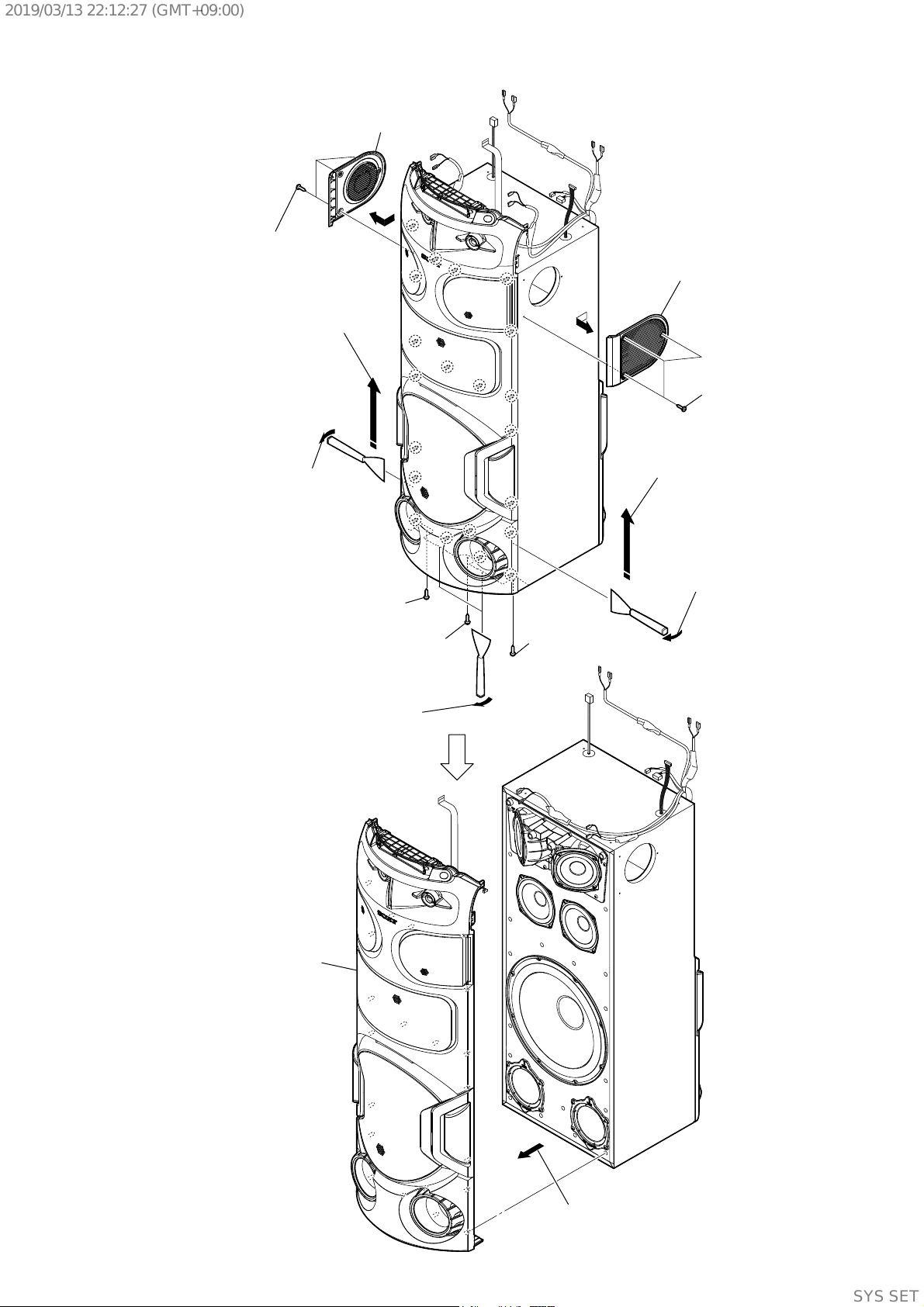
2-13. LOUDSPEAKER (30CM) (WOOFER) (SP9)
:LUHVHWWLQJ
Push the protrusion,
and remove the
terminal (wide side) [grey].
top side
Push the protrusion, and
remove the terminal
(narrow side) [grey/black].
protrusion
MHC-V82D
loudspeaker
(30cm) (woofer)
(SP9)
3 terminal
(wide side)
[grey]
4 loudspeaker (30cm)
(woofer) (SP9)
,QVWDOODWLRQGLUHFWLRQIRUWKH
ORXGVSHDNHUFPZRRIHU63
loudspeaker (30cm)
(woofer) (SP9)
terminal position
1 four screws
((4 u 16),
+BV TAPPING)
3 terminal
(narrow side)
[grey/black]
1 four screws
((4 u 16),
+BV TAPPING)
2 Remove the loudspeaker (30cm)
(woofer) (SP9) in the direction
of the arrow.
21
SYSSET
Page 22

2019/03/1322:12:27(GMT+09:00)
MHC-V82D
2-14. LOUDSPEAKER (10CM) (MID TOP: L-CH) (SP2),
LOUDSPEAKER (10CM) (MID TOP: R-CH) (SP6)
:LUHVHWWLQJ
Push the protrusion,
and remove the terminal
(wide side) [blue].
protrusion
loudspeaker (10cm)
(mid top: L-ch) (SP2)
Push the protrusion, and
remove the terminal
(narrow side) [blue/black].
4 loudspeaker (10cm)
(mid top: L-ch) (SP2)
top side
3 terminal
(narrow side)
[blue/black]
3 terminal
(wide side) [blue]
:LUHVHWWLQJ
Push the protrusion,
top side
Push the protrusion, and
remove the terminal (narrow side)
[red/black].
and remove the
terminal (wide side)
[red].
protrusion
loudspeaker (10cm)
(mid top: R-ch) (SP6)
3 terminal (narrow side)
[red/black]
1 four screws ((4 u 16),
+BV TAPPING)
2 Remove the loudspeaker (10cm)
(mid top: L-ch) (SP2)
in the direction of the arrow.
,QVWDOODWLRQGLUHFWLRQIRUWKHORXGVSHDNHU
FPPLGWRS/FK63
PLGWRS5FK63
loudspeaker (10cm)
(mid top: L-ch) (SP2)
terminal position
loudspeaker (10cm)
(mid top: R-ch) (SP6)
3 terminal
(wide side) [red]
2 Remove the
loudspeaker (10cm)
(mid top: R-ch) (SP6)
in the direction of the arrow.
4 loudspeaker (10cm)
(mid top: R-ch)
(SP6)
1 four screws
((4 u 16),
+BV TAPPING)
22
SYSSET
Page 23

2019/03/1322:12:27(GMT+09:00)
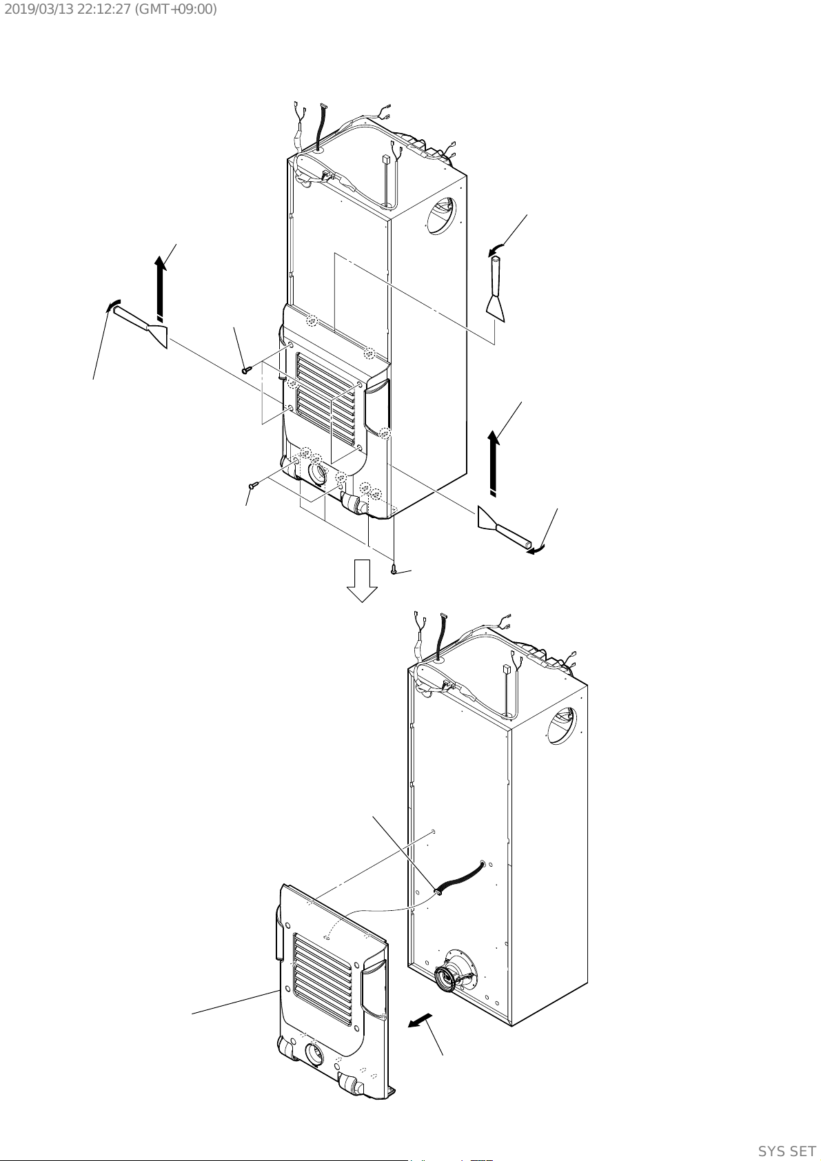
2-15. LOUDSPEAKER (12CM) (MID BOTTOM: L-CH) (SP1),
LOUDSPEAKER (12CM) (MID BOTTOM: R-CH) (SP5)
:LUHVHWWLQJ
Push the protrusion, and
remove the terminal
(wide side) [blue].
top side
loudspeaker (12cm)
(mid bottom: L-ch)
(SP1)
protrusion
MHC-V82D
3 terminal (narrow side)
[red/black]
3 terminal
(wide side) [blue]
3 terminal (narrow side)
[blue/black]
2 Remove the
loudspeaker (12cm)
(mid bottom: L-ch) (SP1)
in the direction of the arrow.
4 loudspeaker (12cm)
(mid bottom: L-ch) (SP1)
3 terminal
(wide side)
[red]
Push the protrusion, and
remove the terminal
(narrow side) [blue/black].
,QVWDOODWLRQGLUHFWLRQIRUWKHORXGVSHDNHU
FPPLGERWWRP/FK63
PLGERWWRP5FK63
1 four screws ((4 u 16),
+BV TAPPING)
1 four screws ((4 u 16),
+BV TAPPING)
2 Remove the loudspeaker (12cm)
(mid bottom: R-ch) (SP5)
in the direction of the arrow.
terminal position
4 loudspeaker (12cm)
(mid bottom: R-ch) (SP5)
:LUHVHWWLQJ
Push the protrusion, and
remove the terminal
(wide side) [red].
loudspeaker (12cm)
(mid bottom: R-ch)
(SP5)
top side
loudspeaker (12cm)
(mid bottom: L-ch)
(SP1)
loudspeaker (12cm)
(mid bottom: R-ch)
(SP5)
protrusion
Push the protrusion, and
remove the terminal
(narrow side) [red/black].
23
SYSSET
Page 24

2019/03/1322:12:27(GMT+09:00)
MHC-V82D
SECTION 3
TEST MODE
PANEL TEST MODE
This mode is used to check the screen display panel, LEDs, buttons, touch keys and GESTURE CONTROL sensor.
Procedure:
1. Press [
2. Touch [] touch key and [VOICE CHANGER] touch key si-
3. All LEDs and segments in screen display panel are lighted up.
Touch [N] touch key repeatedly to toggle diff erent display
Segments on screen display panel:
All On → 1st Group On → 2nd Group On → All On → All Off
Single color LEDs:
All On → All Off → 1st Group On → 2nd Group On → All Off
Multi Color LEDs:
All On → Red → Green → Blue → All Off
4. Touch [ -] touch key, the key check mode is activated.
5. In the key check mode, the screen display panel displays
Each time a button/touch key is pressed/touched, “K”
The screen display panel displays “<” or “>” or “˄” or
6. To release from this mode, touch the touch keys in the same
MODEL, DESTINATION AND VERSION DISPLAY MODE
This mode is used to check the model, destination and software
version of the set.
Procedure:
1. Press [
2. Touch [] touch key and [VOICE CHANGER] touch key si-
All segments in screen display panel are lighted up.
3. Touch [ +] touch key. Model information appears on the
4. Touch [ +] touch key again. Destination information appears
5. Touch [ +] touch key. Serial number appears on the screen
6. During the serial number display, touch [ +] touch key. Each
7. Touch [] touch key and [VOICE CHANGER] touch key si-
1] button to turn on the system.
multaneously for 3 seconds.
This is the display check mode.
mode as below.
“K 0”.
value increases. However, once a button/touch key has
been pressed/touched, it is no longer taken into account.
After all the buttons/touch keys have been pressed/
touched, “K” value will toggle between “OK” and “K30”.
“˅” on the right side of “K30 OK” each time swing left,
right, up and down at GESTURE CONTROL.
manner as step 2, or disconnect the power cord.
1] button to turn on the system.
multaneously for 3 seconds.
screen display panel.
on the screen display panel.
display panel.
time [ +] touch key is touched, the screen display panel
shows the version of each category software in the following
sequence: SC, MTK, BT, BTE, TS, PF, SUB and return back
to model information display.
multaneously for 3 seconds to exit.
COLD RESET
This mode is used to reset all the user settings to factory setting.
Execute this mode when returning the unit to the customer.
Procedure:
1. Press [1] button to turn on the system.
2. Touch [] touch key and [VOCAL FADER] touch key simultaneously for 3 seconds.
3. “COLD RST” appears on the screen display panel. After that,
“SONY” appears on the screen display panel. The system automatically turn on and off once. Please be sure that the system
stay at demo mode fi nally before switch off the power supply.
DISC TRAY LOCK
When the disc tray does not open and “LOCKED” appears on the
screen display panel, disc tray lock mode has been activated by the
shop front.
To release from Disc Tray Lock Mode
1. Press [
2. Touch [FUNCTION] touch key repeatedly to select DVD/CD
3. Touch [MEGA BASS] touch key and [VOCAL FADER]
SHOP FRONT DEMO
The playback started automatically and the “ * DEMO * ” appears
on the screen display panel.
This is the Shop Front Demo mode which is activated by the shop
front.
To release from Shop Front Demo Mode
1. Touch [] touch key and [MIC ECHO] touch key simultaneously
2. The message “STANDBY” blinks for a few times and the
1] button to turn on the system.
function.
touch key simultaneously and hold down until “UNLOCKED”
displayed on the screen display panel.
for 5 seconds.
system goes to demo mode.
USER RESET
The user reset clears all data including preset data stored in the data
fl ash to initial conditions.
Procedure:
1. Press [
2. Touch [GUITAR] touch key and [MEGA BASS] touch key si-
3. “RESET” appears on the screen display panel. After that, the
1] button to turn on the system.
multaneously for 3 seconds.
screen display panel becomes blank for a while, and the system
goes to demo mode.
24
SYSSET
Page 25

2019/03/1322:12:27(GMT+09:00)
MHC-V82D
SECTION 4
ELECTRICAL CHECK
TUNER SECTION
0 dB = 1 ȝV
FM AUTO STOP CHECK
signal
generator
set
+
75
–
Procedure:
1. Turn the power on.
2. Input the following signal from Signal Generator to FM
antenna input directly.
Carrier frequency : A = 87.5 MHz, B = 98 MHz, C = 108 MHz
Deviation : 75 kHz
Modulation : 1 kHz
ANT input : 35 dBu (EMF)
Note: Please use 75 ohm “coaxial cable” to connect SG and the
set. You cannot use video cable for checking.
Please use SG whose output impedance is 75 ohm.
Checking Location:
-MOTHERBOARD Board (Component Side)-
pin 17 (RF)pin 1 (GND)
CN302
3. Set to FM tuner function and scan the input FM signal with
automatic scanning.
4. Confi rm that input Frequency of A, B and C detected and
automatic scanning stops.
The stop of automatic scanning means “The station signal is
received in good condition”.
FOCUS BIAS CHECK
oscilloscope
(DC range)
MOTHERBOARD board
CN302 pin 17 (RF)
CN302 pin 1 (GND)
+
–
Procedure:
1. Connect the oscilloscope to CN302 pin 17 (RF) and CN302
pin 1 (GND) on the MOTHERBOARD board.
2. Press the [
] button to turn the power on, and touch the
1
[FUNCTION] touch key to select DVD/CD function.
3. Set the test disc (CD: YEDS-18) on the tray and touch [N]
touch key to playback.
4. Confi rm that oscilloscope waveform is as shown in the fi gure
below (eye pattern).
A good eye pattern means that the diamond shape () in the
center of the waveform can be clearly distinguished.
VOLT/DIV: 200 mV
TIME/DIV: 500 ns
level:
1.1 ± 0.25 Vp-p (DVDSL)
1.0 ± 0.25 Vp-p (CD)
25
SYSSET
Page 26

2019/03/1322:12:27(GMT+09:00)
MHC-V82D
Check whether the state of the Cable and Outlet are
normal. If there are no problems, check circumference
circuit for Main ON on Output of the Motherboard mount
side.
SECTION 5
TROUBLESHOOTING
Replaces SMPS board (EMC) if it is not up to standard.
No
Yes
AC IN
The Power Control signal to SMPS board (EMC) is checked.
Is following power voltage OK?
Main ON Standby Demo mode Power On
NO6501 Pin9 Low (0V) Hi (3.3V) Hi (3.3V)
(4)
(5)
No
17.4V±5%
58.5V±5%
17.4V±5%
Yes
Standby Demo mode Power On
17.4V±5%
58.5V±5% 58.5V±5%
NO6501 Pin1, 4, 5
The Output from SMPS board (EMC) is checked.
Is following power voltage up to standard?
CN6500 Pin6, 7, 8, 9
END
(1)
SMPS Board (EMC) Diagnosis Flow
26
(3)
(2)
Pin 1: Audio (+17V)
Pin 3: Audio (GND)
(1) AC input
(2) Fuse
(3) MAIN power transformer
(4) NO6501 connector
Pin 4: LED (+17V)
Pin 5: LED (+17V)
Pin 6: LED (GND)
Pin 7: LED (GND)
Pin 8: AC DET
Pin 9: Main ON
Pin 10: Network ON
Pin 11: Low/ High AC
Pin 12: Latch ON
(5) CN6500 connector
Pin 1: PGND
Pin 3: PGND
Pin 4: PGND
Pin 5: PGND
Pin 6: PVDD (DC+58.5V)
Pin 7: PVDD (DC+58.5V)
Pin 8: PVDD (DC+58.5V)
Pin 9: PVDD (DC+58.5V)
SYSSET
Page 27

2019/03/1322:12:27(GMT+09:00)
MHC-V82D
Checks IC303 circumference circuit for +1.2V.
Checks IC009 (JL071) circumference circuit for +3.3V.
No
Checks JL355 for +3.3V and CL308 +1.2V REG IC303.
Does it output the power voltage of 3.3V and 1.2V?
No
Checks circumference circuit for SL+/SL- of IC401.
Checks circumference circuit of IC301 FMO Signal.
No
Yes
Yes
Does it output the signal?
Checks CN402 SL+/SL- signal.
The Sled motor has a problem.
Replaces BU.
Checks circumference circuit for SP+/SP of IC401.
Checks circumference circuit of IC301 DMO Signal.
No
Yes
Does it output the signal?
Checks CN402 SP+/SP- signal.
No
The Spindle motor has a problem.
Checks circumference circuit for FCS+/FCS- of IC401.
No
Replaces BU.
Checks CN302 FCS+/FCS- signal.
No
Checks circumference circuit of IC301 FOO Signal.
Yes
The Optical pickup has a problem.
Does it output the signal?
Replaces BU.
Yes
REMOVE SIDE PANEL
REMOVE TOP PANEL
TURN ON
TRAY IN
(Visual check)
Optical Block Diagnosis Flow (1/2)
Does Optical pickup move to inner circumference?
Yes
Does Spindle motor rotate?
(Visual check)
Yes
Does Optical pickup do focus search?
(Visual check)
A
27
SYSSET
Page 28

2019/03/1322:12:27(GMT+09:00)
MHC-V82D
Checks circumference circuit of Q402.
Checks circumference circuit of IC301 LDO1.
Replaces BU if it is not up to standard.
No
Yes
The Optical pickup has a problem.
Checks JL306 (LD780) signal.
Does it output 2V when laser become luminous?
No
Replaces BU.
If it is not up to standard,
No
No
Yes
Lens cleaning is performed.
Is output level of RF signal JL317 up to standard?
Yes
RF Level = 1.05 ±0.45 Vpp
Test disc (CD: YEDS-18, DVD: HLX-503 (NTSC) or HLX-504 (PAL))
No
The Optical pickup has a problem.
Replaces BU.
A
Optical Block Diagnosis Flow (2/2)
Does laser diode become luminous?
28
Yes
(Visual check)
Yes
DISC IN
Yes
Is output level of RF signal JL317 up to standard?
RF Level = 1.05 ±0.45 Vpp
Test disc (CD: YEDS-18, DVD: HLX-503 (NTSC) or HLX-504 (PAL))
Yes
END
Is there no problem with Long term Aging Test (60min)?
Confirms that there is no sound skip.
SYSSET
Page 29

2019/03/1322:12:27(GMT+09:00)
MHC-V82D
Check and replace the speaker.
Yes
Yes
No
Yes
Exchange IC2002.
No
Exchange IC3503.
Yes
No
"PROTECT3" is not displayed, when removing the speaker connector
"PROTECT3" is displayed on the screen display panel after turning the
MOTHERBOARD Mount Amplifi er Diagnosis Flow (1/3)
1. “PROTECT3” is displayed after turning the power on
power on.
(CN2005 and CN3502) and turning the power on.
Check that IC2002 pin 27, 32, 35 and 39 is short to GND/PVDD.
Check that IC3503 pin 27, 32, 35 and 39 is short to GND/PVDD.
MOTHERBOARD board damaged. Exchange the MOTHERBOARD mounted pc board.
29
SYSSET
Page 30

2019/03/1322:12:27(GMT+09:00)
MHC-V82D
MOTHERBOARD board damaged. Exchange the MOTHERBOARD mounted pc board.
No
Yes
Yes
No
Exchange IC2001.
Yes
No
Exchange IC2002.
Yes
Exchange IC3503.
No
Yes
MOTHERBOARD Mount Amplifi er Diagnosis Flow (2/3)
2. The sound is not outputted
The sound is not outputted.
30
Check that the signal is input to IC2001 pin 24 and 25.
Check that the PWM signal is outputted from IC2001 pin 38, 39, 40 and 41.
Check that the signal is outputted from IC2002 pin 35 and 39 (Left channel
speaker), pin 27 and 32 (Right channel speaker).
Check that the signal is outputted from IC3503 pin 27, 32, 35 and 39
(Subwoofer speaker).
MOTHERBOARD board damaged. Exchange the MOTHERBOARD mounted pc board.
SYSSET
Page 31

2019/03/1322:12:27(GMT+09:00)
MHC-V82D
Yes
Exchange original damaged IC.
Yes
No
First time repair?
MOTHERBOARD board damaged. Exchange the MOTHERBOARD mounted pc board.
No
Assembly back the set.
MOTHERBOARD Mount Amplifi er Diagnosis Flow (3/3)
3. IC and MOTHERBOARD board after replace checking guide
After IC2002, IC3503 and MOTHERBOARD board change, check as below:
Make sure connect the connector (CN2005 and CN3502).
Volume set to Max, sound field set to default, Mega Bass set to “ON”.
Play song “Billie Jean By Michael Jackson” for 2 minutes.
Check for any abnormality:
Protect 3 is displayed/ Set Reset to DEMO/ No display etc.
Repair is successful.
31
SYSSET
Page 32

2019/03/1322:12:27(GMT+09:00)
MHC-V82D
Tes ter
Tes ter
JL2020
JL2021
JL2030
CL3554
C3599
Tes ter
CL3543
CL3530
CL3535
Tes ter
JL3501
CL3581
CL3580
CL2028
CL2029
JL2026
CL2030
Tes ter
CL2031
JL2029
C2090
JL2035
C2151
IC1000
JL905
JL110
JL111
C1003
C1005
C1009
JL631
C1013
R1026
C1010
JL1003
Tes ter
JL619
Tes ter
JL620
Tes ter
JL101
JL102
C639
3
12
L605
R937
CN900
4
JL901
C930
L900
C931
C932
A/K
KA
L901
D900
JL900
R940
C2224
C2222
C2220
JL2201
R2206
IC2002 and IC3503 Confi rmation for MOTHERBOARD Mount
C2200
C3588
Tes ter
CL3548
Tes ter
CL3553
CL3536
CL2018
CL2034
Tes ter
Tes ter
CL310
CL309
Tes ter
R1017
IC1001
C1004
R1025
R1024
R1022
C1011
R1027
R1023
C687
JL635
R686
R651
C665
Q605
JL604
R689
C660
R685
JL618
X900
C934
C933
IC902
R943
L902
C936
R939
R944
R2226
JL2221
C2203
C2227
R360
JL330
CL307
CL316
R319
CL395
Q302
R370
CL311
CL313
C306
E
C352
C340
C343
R321
C347
R359
C375
C339
R309
CL380
C351
C346
C344
C348
CL308
Tes ter
RB310
C321
C315
R302R303
R381
R382
C364
JL605
C359
R913
R911
C657
R663
C647
R662
R857
C641
R671
C650
R914
R945
C652
R946
R669
C643
R912
R947
C2218
JL2222
JL2200
JL2223
C2216
JL2202
C2228
JL2224
R2208
R358
JL355
IC303
CL3540
CL3552
JL2011
JL2012
JL2015
JL2005
C350
JL361
C331
CL315
R328
C328
C316
C950
C338
C334
R330
R339
C342
C372
C369
C373
C358
C360
JL2206
C960
36
37
R326
C330
C951
X602
C319
R953
C952
48
C326
R348
JL2203
1
R955
C325
R664
R658
JL357
C981
JL356
C985
C963
JL359
C954
R657
R660
C336
R665
JL358
R981
R352
JL362
L301
C357
C365
C363
C648
C726
R794
R639
JL603
CL3522
CL3518
CL3544
CL3573
CL3574
CL3515
CL3579
CL3531
Tes ter
Tes ter
JL2006
CL2024
JL2003
JL2018
Tes ter
JL2036
JL2009
JL2016
R435
JL313
R959
R637
IC904
R984
R985
R982
R983
R690
R785
C695
R677
R674
C622
C617
JL2207
R412
R957
CL413
25
24
JL305
C949
13
12
R986
R950
R952
R951
R778
R783
R691
R688
R687
C655
C653
IC606
C991
R661
C646
C711
C649
C640
R411
R418
C992
C407
C413
CL408
CL409
28
22
E
Q612
78
1
CL405
CL401
CL403
R407
CL402
CL404
R406
CL3572
R431
IC452
30
29
JL2037
Tes ter
JL2040
R2022
R2021
CL2023
C2019
JL2008
CL414
C423
R389
R432
JL311
R451
R498
JL360
Q304
R304
R314
C409
2115
IC401
C404
JL2034
JL2039
CL2025
CL2022
CL2021
CL2035
CL2020
JL2038
CL2036
R528
R529
Q402
C424
CL415
E
R429
R524
R310
R316
JL304
JL303
R318
JL302
JL306
JL308
JL309
JL301
JL307
JL310
JL314
JL315
JL316
JL318
JL319
JL317
C465
JL324
JL320
JL321
C463
C462
C466
JL322
C311
FB455
JL463
E
JL461
JL462
R305
JL460
E
R478
Q305
JL329
JL323
CL412
R313
CL411
C405
C408
C406
CL410
JL401
14
JL050
C111
R282
C367
C503
C178
R512
R513
JL312
C133
C135
R174
R273
R215
C137
C140
JL325
JL326
C501
R274
JL327
R514
R237
JL328
R230
R148
C146
E
R534
C148
Q1002
JL294
R155
R1007
JL209
JL212
Q1000
E
JL525
C1001
R254
R1001
AK
R1005
D1001
E
Q1005
R1006
Q1001
E
JL524
R1004
R1003
JL144
C1000
R162
R1002
E
R165
R037
R163
Q005
JL024
JL142
R034
JL137
JL136
JL023
JL146
JL022
JL021
JL402
JL130
JL405
JL406
C064
Q013
JL149
JL070
E
C066
R028
C095
C2116
R2147
C2128
CL2011
IC2003
JL2031
C2127
R2146
CL2040
JL269
JL150
R129
R131
R123
R120
IC102
RB105
C102
JL148
R139
R143
TH571
R533
R137
R170
R107
R176
R149
R104
R140
R102
R255
R300
C502
R284
R515
C153
R119
R293
C164
JL138
JL143
JL145
C065
IC003
C118
C114
R175
C112
C280
R222
C115
R103
C506
C504
C117
C168
C283
R283
C160
JL527
C157
C154
C156
C158C159
C155
R153
R154
RB104
RB106
JL529
E
JL528
E
Q111
Q110
IC106
JL526
JL194
R235
JL287
JL147
JL140
R187
JL231
JL523
R505
R507
JL139
JL522
JL230
C008
JL232
JL141
JL520
JL002
IC002
C012
C087
C070
R097
Q2007
C2123
R2102
E
CB
CL2010
R2103
CL2004
AK
KA
D2007
Q2008
R249
R145
R184
R178
C281
R177
C131
C120
C282
C122
C134
C136
RB101
R152
C138
R532
C144
R298
C147
R256
R134
JL115
R135
JL119
R276
JL122
R551
JL155
JL530
JL151
JL521
JL107
JL124
JL123
C2122
R2104
D2008
JL289
JL116
R195
JL121
R552
JL135
L2010
KA
E
R2107
C299
R518
JL109
R546
JL117
JL118
JL120
R122
JL154
JL152
JL106
L2012
CL2038
CL2039
JL2033
D2012
R2106
IC010
R050
C060
C074
JL069
R110
R198
R220
R545
R544
R543
R106
JL134
C165
JL131
JL132
JL153
JL297
JL105
JL068
JL045
C062
JL001
JL003
R068
JL004
Q014
R069
E
R064
R066
E
Q011
JL059
JL008
JL012
R018
JL044
JL175
JL176
JL173
R191
JL196
JL174
JL171
JL172
JL197
JL195
JL199
JL202
JL169
JL235
JL205
JL204
R723
R722R917
R719
C675
R708
C673
C667
C672
R709
C666
R711
JL125
R3009
R3015
R3014
JL108
C3019
CL3010
R060
E
R065
Q012
JL046
JL071
C031
C069
IC007
R015
JL072
JL049
JL198
JL200
JL216
JL201
JL215
JL114
JL203
JL217
JL206
R720
JL613
R792
C678
C671
JL615
C674
IC609
C986
JL910
JL617
JL908
JL909
IC3001
D3005
CL3059
AK
C3018
CL3058
C3000
R3048
JL3002
JL005
R035
R033
R029
C051
E
R070
Q004
C080
JL073
JL047
IC004
IC006
JL048
JL011
JL113
JL614
JL616
JL3007
JL3008
R3047
JL3006
R3046
JL3004
JL3005
JL3001
<Note>
Please check each channel’s resistance value for the Coil’s terminal and Capacitor’s + and – terminal.
7KHVHWHUPLQDO¶VUHVLVWDQFHYDOXHVKRXOGQRWEHQHDUWRȍVKRUW
32
SYSSET
Page 33

2019/03/1322:12:27(GMT+09:00)
6-1. BLOCK DIAGRAM - RS SERVO, USB, TOUCH, HDMI Section -
RF
VOA/A
VOB/B
VOD/C
VOD/D
VC
PD
FE_LD_CD (780)
FE_LD_DVD (650)
SERVICE, OPTICAL
DEVICE (7G)
AUTO
POWER CTRL
Q402
AUTO
POWER CTRL
Q401
CD RF AMP
FOCUS/TRACKING ERROR AMP
CD SYSTEM PROCESSOR
DIGITAL SERVO PROCESSOR
IC301
(1/2)
119
RFIP
RFC
125
124
RFB
123
RFA
126
RFD
HDMI_SCL
5
V20
8
MDI1
128
FE_CD_IOP-
9
LDO1
127
FE_DVD_IOP-
10
LDO2
HDMI_SDA
GPIO10/HPLG
TX2P
TX2N
TX1P
TX1N
TX0P
TX0N
TXCP
TXCN
XTALO
XTALI
USB_DM
USB_DP
MHC-V82D
SECTION 6
DIAGRAMS
CN1000
HOT PLUG DET
+5V POWER
D+
D-
HSD1-
S
10
DATA2+
DATA2–
DATA1+
DATA1–
DATA0+
DATA0–
CLOCK+
CLOCK–
SCL (5V)
SDA (5V)
1
2
1
3
4
6
7
9
10
HDMI OUT
12
(TV) ARC
15
16
19
18
13
14
>001B
ARC_SPDIF
MAIN SECTION
(Page 34)
CN4100
3
D+
2
D-
VBUS
REC/PLAY
5V 1A
1
94
93
91
90
88
87
85
84
28
29
81
4
X301
27MHz
3
20
19
CEC DATA SWITCH
Q1000 ~ Q1002, Q1005
ARC BUFFER
IC1001
3A
6
2
3Y
2A
3
5
2Y
USB SWITCH
6
HSD2-
HSD2+
7
5
+5V
IC453
HSD1+
4
(LO:DVD,HI:CD)MSW
CONNECT TO
MS-476 BOARD
CD_VR(780)
DVD_VR(650)
FCS+
FCS–
TRK+
TRK–
SL+
SL–
SP+
SP–
CN303
LOAD-
1
LOAD+
2
TRAY-IN
3
TRAY-OUT
5
151
106
MSW
18
CD_VR
14
DVD_VR
15
SF_CS_
24
SF_DO
25
SF_DI
5CH SYSTEM
MOTOR DRIVER
IC401
14
13
16
15
17
18
11
12
9
10
VOTRVOTR+
FOCUS
COIL DRIVER
FOCUS
COIL DRIVER
FOCUS
COIL DRIVER
FOCUS
COIL DRIVER
BIAS
MUTE
FWD
REV
FOO
1
4
23
26
27
28
6
7
17
DMO
12
FMO
13
TRO
16
V14
6
108
MUTE
SF_CK
26
27
EEPROM
IC302
1
CS
2
DO(IO1)
5
DI(IO0)
6
CLK
DQ0 – DQ15 A0 – A11
2, 4, 5, 7, 8, 10, 11, 13, 42,
44, 45, 47, 48, 50, 51, 53
41 – 48, 58 – 50 75 – 78, 67 – 61
RD0 – RD15 RA0 – RA11
64M SDRAM
29 – 34, 22, 35
IC306
23 – 26,
BA0
BA1
LDQM
UDQM
DQM0
DQM1
RAS
RAS#
CAS
CAS#
PRST_
GPIO13
CLK
20 21 38 15 39 18 17 16
72 73 60 49 59 70 69 68
BA0
BA1
RCLK
WE
RWE#
IFSDI
IFSDO
IFSCK
IFCS_
10
15
35
38
37
32
34
36
22
20
17
14
19
104
8
3
12
13
150
DP0
DM0
VBUS-OE/SD_WP_0
USB-OC/SD_LED0
CEC-IN (DVD)
CEC-OUT (DVD)
SYSTEM
CONTROL
IC109 (1/4)
TOUCH-INT1/GUITAR-LED
TOUCH-NFC_SDA
TOUCH-NFC_SCL
MTK-SDO
MTK-SDI
MTK-CLK
MTK-RESET
MTK-XIFCS
MTK-BUSY
CD-MOTOR+
CD-MOTOR-
CDM-LOAD0-SW
CDM-UNLOAD-SW
USB-HOST-SEL
129
112
35
51
130
TOUCH CONTROLLER
IC5202
2
EXTCLK/PA3
PA1
20
PA2
1
PB2/TOSC2
USB HI-SIDE SWITCH
IC452
3
EN
4
FLAG
OUT
PC0 – PC3
5, 7, 8, 9, 10, 13 – 18
PA4, 6, 7, PB0, 1, 4, 5,
12
6
IN
1
USB+5V
PARTY LIGHT
PARTY CHAIN
WIRELESS PARTY CHAIN
MEGA BASS
FIESTA
PAIRING BLUETOOTH
GESTURE ON/OFF
FUNCTION
PLAYBACK
DJ
N
x
SAMPLER
KARAOKE
TUNING - .
TUNING + >
Z
SOUND FIELD
VOLUME +
VOLUME -
+
-
MIC/GUITAR LEVEL +
MIC/GUITAR LEVEL MIC ECHO
VOCAL FADER
VOICE CHANGER
GUITAR
LED DRIVER
Q5009
6LJQDOSDWK
: AUDIO DIGITAL
: VIDEO
: CD PLAY
: USB
D5200
MHC-V82D
3333
SYSSET
Page 34

2019/03/1322:12:27(GMT+09:00)
MHC-V82D
6-2. BLOCK DIAGRAM - MAIN Section -
AUDIO/PARTY CHAIN
IN (TV)
ANTENNA
FM
J602 (1/2)
CN900
2
X900
12MHz
RL
(FM RECEIVER)
1
FRF1
16
X1
X2
17
AUDIO/PARTY CHAIN
IN (TV)
J4100
MIC1
J4101
MIC2
GUITAR
FM DRIVER
IC902
CK
DA
IIC/RDSI
LRCK/LOUT
BCLK/ROUT
IISD
AUDIO/PARTY CHAIN
OP AMP
IC601
+
+
OUT
J602 (2/2)
OUT
OUT
DOUT0_AMP
DIN0
MCK
BCK
LRCK
ARC_SPDIF
MUTE
PROTECT
Q602
MUTE SW
Q606
BIAS
DETECTOR
RXIN3
LRCK
BCK
32
RST
834262821424
Q605, Q607
4
47
293033
MIC AMP
IC4100
6
STEREO A/D
IC606
75
126 125
6
109
ACLK SCKI
ASDATA0
13
VINL
14
VINR
7
LRCK
88
BCK
910
DOUT
ALRCK
114
115
ABCK
110
X602
24.576MHz
STEREO A/D
CONVERTER
MPIO_C2/ALRCK_I1
9
MPIO_C1/ABCK_I1
MPIO_C3/ADIN_1
RXIN6/ALRCK_I0
29
RXIN7/ADIN_0
28
30
RXIN5/ABCK_I0
25
MC/SCL
24
MDI/SDA
12
MPIO_B1/ABCK_I2
13
MPIO_B2/ALRCK_I2
MPIO_B3/ADIN_2
14
40
XTO
XTI
39
ERROR/INT0
1 2 17 18 19 34
IC904
MPIO_A1
NPCM/INT1
DOUT
13
SWITCHING
CONTROL
Q001
CONVERTER
CD RF AMP
FOCUS/TRACKING ERROR AMP
CD SYSTEM PROCESSOR
DIGITAL SERVO PROCESSOR
8
11
6
13
12
14
2
5
11
3
6
10
SIGNAL
SELECTOR
IC905
1A
2A
3A
1B
2B
3B
7
2Y
1Y
4
9
3Y
52120
45
114
IC301
(2/2)
STEREO A/D
CONVERTER
IC609
13
VINL
14
VINR
9
DOUT
7
LRCK
8
BCK
6
SCKI
STEREO D/A
CONVERTER
IC604
7
VOUTL
8
VOUTR
SCK
16
BCK
1
LRCK
3
DATA
2
43
OP AMP
IC603
OUT
31
++OUT
75
SIGNAL
SELECTOR
Y1
5
X1
14
Y0 A
1
12
X0
IC602
Y
33 1
X
13 5 7
10
ANALOG
SELECTOR
Q612
AUDIO/PARTY CHAIN
RL
LINK SET
OUT
Q603
>002B
AMP
SECTION
(Page 35)
>001B
RS SERVO, USB, TOUCH,
HDMI SECTION
(Page 33)
MHC-V82D
CP IC
IC3000
SCL
SDA
SSI3-DI
DIR-INT0
DIR-INT1
SSI3_BCKO
SSI3_LRCKO
USB-X1
USB-X2
140 169 172 166 170 168 167
139
X104
48MHz
LINK-DET
DIR-RESET/SD_LED1
SSI0_BCKO
SSI0_LRCKO
SSI0_DI(MIC)
AUDIO-CLK-OUT
Q-Flash-CS
123567
CS
Q-Flash-SIO1
Q-Flash-SIO0
Q-Flash-SIO2
DI(IO0)
DO(IO1)
WP(IO2)
EEPROM
IC106
Q-Flash-SIO3
Q-Flash-CLK
IO3
CLK
/LINE-MUTE
LINK-SET
48
175
6LJQDOSDWK
: AUDIO
: TUNER (FM)
: AUDIO DIGITAL
: MIC
65
ST-RDS
MIC-DET1
MIC_DET2
MODE-SEL
DIR-TUNER-SCL
DIR-TUNER-SDA
BT-ON
BT-RXD(MD-CLK)
65
16 70 71 9291
EXTAL
X105
13.333 MHz
XTAL
SYSTEM CONTROL
IC109 (2/4)
AUDIO-X1
AUDIO-X2
X103
12.288MHz
CP3000
BLUETOOTH MODULE
RFS0
2
SCLK0
3
DT0
4
HCI_RXD
19
MFB
26
EAN
32
P2_0
41
A1
B1
15
16
CP_SCL
CP_SDA
HCI_TXD
RST_N
20
13
RESET IC
IC3001
VOUT VDD
24
BT-TxD
133
MFB
164
165
EAN
124
P20
BUS BUFFER
IC102 (1/2)
2A 2Y
BLUETOOTH
POWER CONTROL
Q103, Q104
3434
SYSSET
Page 35

2019/03/1322:12:27(GMT+09:00)
6-3. BLOCK DIAGRAM - AMP Section -
MHC-V82D
>002B
MAIN
SECTION
(Page 34)
DOUT0_AMP
DIN0
MCK
BCK
LRCK
STREAM PROCESSOR
IC2001
29
SDOUT
27
SDIN4
11
MCLK
23
SCLK
22
LRCLK
SDIN3
26
SDIN2
25
24
SDIN1
21
SCL
SDA
20
16
RESET
19
MUTE
PWM_P_1
PWM_M_1
PWM_P_2
PWM_M_2
VALID
PWM_P_4
PWM_M_4
DIGITAL POWER AMP
IC2002
OUT_A_39 39
OUT_A_40 40
OUT_B 35
OUT_C
OUT_D_27
OUT_D_28 28
DIGITAL POWER AMP
IC3503
OUT_C
OUT_D_27
OUT_D_28 28
OUT_A_39 39
OUT_A_40 40
OUT_B 35
32
27
32
27
FAN RESET
SWITCH
Q2005
15
4
16
17
4
16
17
INPUT_C14
INPUT_D
INPUT_A5
INPUT_B6
RESET
FAULT
OTW
RESET
INPUT_A5
INPUT_B6
FAULT
OTW
39
38
41
40
37
49
48
L2002
L2002
L2003
L2003
L3509
L3509
L3511
L3511
F+13V
5.2V
FAN DRIVER
Q2006
FAN DRIVER
Q2000
FAN DRIVER
Q2008
FAN DRIVER
Q2007
L-CH
R-CH
SW
CN2001
DC FAN
CN2008
DC FAN
54
30
131 132
32 40
SSI2-DO(FR)
SSI0_LRCKO
SSI1_DO(TW)
SSI0_DO(PARTY CHAIN)
53
PWM_SCL
PWM_SDA
57
DAMP-MUTE
/AMP-RESET
SYSTEM CONTROL
IC109 (3/4)
49
/SD-FAST
78
AMP-PROTECT
FAN PROTECTION
(LOCK)
Q2002
6LJQDOSDWK
: AUDIO
: AUDIO DIGITAL
MHC-V82D
3535
SYSSET
Page 36

2019/03/1322:12:27(GMT+09:00)
MHC-V82D
6-4. BLOCK DIAGRAM - PANEL, POWER SUPPLY Section -
VACUUM
FLUORESCENT
DISPLAY
ND4000
D4463~D4465
D4493~D4495
D5307~D5310
D4440, D4442,
D4450, D4452
SPK MID L/R:
D4400, D4410
SPK MID BTM:
D4600, D4601
D4473~D4475
D4483~D4485
D5001
D5000
D5005
D5002
D5003
D5006
D5007
D5008
SW LED L/R:
DIN
CLK
STB
VIN
F+
GESTURE CONTROL
GESTURE CONTROL
EAST ELECTRODE
GESTURE CONTROL
SOUTH ELECTRODE
GESTURE CONTROL
WEST ELECTRODE
GESTURE CONTROL
NORTH ELECTRODE
POWER CONTROL
PROTECTION
Q4001,Q4002
TRANSMITTER
LED DRIVER
IC2200
OUT1
I
OUT6
OUT9
I
14 - 19 6 - 11
OUT14
LED DRIVER
IC5001
OUT0
I
OUT7
OUT9
I
OUT11
OUT12
I
17 - 19 5 - 1214 - 16
OUT14
20
OUT15
13
OUT8
LED DRIVER
IC5002
OUT0
I
5- 614-1617-20
OUT1
7
OUT2
OUT3
I
OUT5
OUT6
I
11-13 8-10
OUT8
OUT9
I
OUT11
OUT12
I
OUT15
LED DRIVER
IC4300
OUT2
I
7 - 12
OUT7
OUT8
I
13 - 18
OUT13
M+5.2V
REMOTE CONTROL
RECEIVER
GESTURE CONTROLLER
25
4
6
7
8
SIN
2
SCK
3
TRANS
4
PWMCLK
21
SIN
2
SCK
3
TRANS
4
PWMCLK
21
SOUT
22
SIN
2
SCK
3
TRANS
4
PWMCLK
21
SOUT
22
SIN
2
SCK
3
TRANS
4
PWMCLK
21
IC4200
TXD
RX0
RX2
RX3
RX4
FL+12V
S4221
S4220
TAIKO
IC5300
EIO0
EIO4/SI0
EIO5/SI1
MCLR
C-CONT
ST-CE
RES
LATCH-ON
79
PROTECTION
Q011
BUS BUFFER
IC102 (2/2)
PROTECTION CONTROL
Q576
PROTECTION CONTROL
Q575
PROTECTION CONTROL
Q574
PROTECTION CONTROL
Q572
PROTECTION CONTROL
Q571
AC CUT SWITCH
12
4A
TO
AMP
SECTION
Q107
PVDD
SMPS
MAIN-ON
NETWORK ON
V1
M/D_+13V/+16V
A+13V
(AC IN)
AC-DET
LOW/HIGH AC
LATCH ON
118
82
D+3.3V
122
55
+1.2V
POWER CONTROL
PROTECTION
Q302, Q303
112
59
+3.3V REG.
SDA
SCL
RFDET
TH571
NFC
IC001
VOUT
3
CE
1
+3.3V
44
60
130
129
137
80
76
63
96
27
5
6
7
VO VCC
16
+1.2V REG.
POWER CONTROL
PROTECTION
Q304,Q305
IC903
VDD
4
DETECTOR
4
FAULT
POWER CONTROL
PROTECTION
POWER CONTROL
PROTECTION
IC303
+5V
VOLTAGE
IC007
OUT
6
Q008
Q009
POWER CONTROL
POWER CONTROL
1
CONT
4
VOUT
1
IN
PROTECTION
Q005
PROTECTION
Q010
+5V REG.
IC1000
+5V REG.
IC006
+5V
+5.2V
POWER CONTROL
PROTECTION
POWER CONTROL
PROTECTION
POWER CONTROL
PROTECTION
VIN
5
SW_12V
Q013
Q006
Q007
M+5.2V
M+5.2VPNL
+12V REG.
SW+12V
VOLTAGE REGULATOR
PG1
6
PG2
11
SW2
14
+1.2V SW1
+9V REG.
IC2000
+3.3V
A+13V_AMP
IC004
3
POWER CONTROL
PROTECTION
POWER CONTROL
6
OUT
FAULT
4
EN
3
POWER CONTROL
EN
3
4
FAULT
6
OUT
INOUT
+12V REG.
IC002
5
EN
1
OUT
RESET IC
IC103
IC009
Q110,Q111
IC010
IC003
USB+5V
VCC
VOUT
VIN1
VIN2
F+13V
IN
IN
8
4
1
16
VOLTAGE REGULATOR
SW2
1
14
1
EN212
PG2
11
EN1
5
SW1
3
POWER CONTROL
PROTECTION
Q004
POWER CONTROL
PROTECTION
Q014
PROTECTION
SWITCH
Q012
+12V REG.
IC2003
OUT IN
IC001
VIN1
VIN2
1
16
POWER CONTROL
1
1G
2G
4
3G
10
13
4G
4Y
11
FL-SOUT
4
FL-CLK
2
176
FL_LATCH
POWER-KEY
6
AD-KEY0/TAIKO-KEY
84
135 SIRCS
111
12
20
21
24
3D-DETECT/SD_D1_0
3D (GESTURE)_SDA
128
3D (GESTURE)_SCL
127
3D-RESET/TEST-MON103/SD_D2_0
103
RGB-SOUT
117
134
RGB-SCLK
173
RGB-TRANS-LED
RGB-PWM-CLK
136
SYSTEM CONTROL
IC109 (4/4)
PCONT-PSAVE-PROTECT
SPM-C-MON
PCONT-DAMP
PROTECTOR
PCONT-BTSTBY
VBUS-OE/SD_WP_0
MTK-POWER-CTRL
TOUCH-NFC_SDA
TOUCH-NFC_SCL
NFC-RF-DET
SPM-AMBIENT-TEMP
AC-CUT(MD-BOOT0)
LOW_AC-DET/SD_PCON
MHC-V82D
3636
SYSSET
Page 37

2019/03/1322:12:27(GMT+09:00)
6-5. BLOCK DIAGRAM - SMPS Section -
LOW/HIGH AC
SWITCH
Q6509
MHC-V82D
LOW/HIGH AC
+13V
RECT
D6000
RECT
D6001
CONVERTER
TRANSFORMER
(MAIN)
T6300
V1
RECT
D6504
RECT
D6501
SHUNT REGULATOR
IC6500
SWITCHING
TRANSISTOR
TH6000
OVERLOAD
PROTECTION
Q6302, Q6303Q6300, Q6301
DETECT
SWITCH
Q6307
OVERLOAD
PROTECTION
Q6304
OVERLOAD
PROTECTION
Q6306
F6000
DETECT
SWITCH
Q6305
CN6000
(AC IN)
TH6300
ISOLATOR
PH6300
ISOLATOR
PH6302
AC-DETECT
SWITCH
Q6500
LATCH ON
SWITCH
Q6506,Q6507
POWER CONTROL
IC6300
HV
8
1
LATCH
5
DRV
VCC
6
2
FB
AC_DET
LATCH ON
VREF
NETWORK ON
SWITCH
Q6501
MAIN ON
SWITCH
Q6504
12
K
ISOLATOR
PH6301
NETWORK ON
MAIN ON
MHC-V82D
3737
SYSSET
Page 38

2019/03/1322:12:27(GMT+09:00)
MHC-V82D
• Note for Printed Wiring Boards and Schematic Diagrams
Note on Printed Wiring Board:
• X : parts extracted from the component side.
•
: parts extracted from the conductor side.
• : Pattern from the side which enables seeing.
(The other layer’s patterns are not indicated.)
Caution:
Pattern face side:
(Conductor Side)
Parts face side:
(Component Side)
• MOTHERBOARD board is multi-layer printed board. However,
the patterns of intermediate layers have not been included in
diagrams.
• Indication of transistor.
C
Q
B
E
D
Q
G
S
Q
B
CE
Q
B
CE
Note 1: When the MOTHERBOARD board is replaced,
spread the compound referring to “NOTE OF
REPLACING THE IC2002 AND IC3503 ON
THE MOTHERBOARD BOARD AND THE
MOTHERBOARD MOUNTED PC BOARD” on
servicing notes (page 6).
Parts on the pattern face side seen from
the pattern face are indicated.
Parts on the parts face side seen from
the parts face are indicated.
These are omitted.
These are omitted.
These are omitted.
These are omitted.
Note on Schematic Diagram:
• All capacitors are in μF unless otherwise noted. (p: pF)
50 V or less are not indicated except for electrolytics
and tantalums.
• All resistors are in and 1/4 W or less unless otherwise
specifi ed.
• f : Internal component.
• 2 : Nonfl ammable resistor.
• 5 : Fusible resistor.
• C : Panel designation.
Note: The components identifi ed by mark 0 or dotted
Replace only with part number specifi ed.
• A : B+ Line.
• B : B– Line.
• H : Adjustment for repair.
• Voltage and waveforms are dc with respect to ground
under no-signal (detuned) conditions.
( ) : CD PLAY
{ } : DVD PLAY
[ ] : USB
< > : Bluetooth
* : Impossible to measure
• Voltages are taken with a VOM (Input impedance 10 MΩ).
Voltage variations may be noted due to normal production
tolerances.
• Waveforms are taken with a oscilloscope.
Voltage variations may be noted due to normal production
tolerances.
• Circled numbers refer to waveforms.
• Signal path.
F : AUDIO
f : TUNER (FM)
L : CD PLAY
E : VIDEO
d : USB
J : AUDIO DIGITAL
N : MIC
line with mark 0 are critical for safety.
no mark : TUNER
• Circuit Boards Location
POWER K E Y board
SMPS board (EMC)
MS-476 board
HUB board
SPK MID L board
SPK MID R board
SPK MID BTM board
360 FR L board
SW LED L board
SENSOR board
VFD board
MIC USB board
NFC board
MOTHERBOARD board
IR board
360 BACK L board
EXTENSION board
360 BACK R board
360 FR R board
SW LED R board
Note 2: When the MS-476 board is defective, exchange
the entire LOADING COMPLETE ASSY (T).
Note 3: When the SENSOR board is defective, exchange
the VICENTE TOP PANEL ASSY SERVICE.
Note 4: When the MOTHERBOARD mounted pc board
is replaced, be sure to refer to “DESTINATION
SETTING METHOD” on page 5.
MHC-V82D
3838
SYSSET
Page 39

2019/03/1322:12:27(GMT+09:00)
6-6. PRINTED WIRING BOARD - MOTHERBOARD Board (Component Side) - • See page 38 for Circuit Boards Location. • : Uses unleaded solder.
MHC-V82D
1
A
B
C
SMPS BOARD (EMC)
CN6500
(Page 43)
D
E
F
G
H
I
J
K
2 3 4 5 6 7 8 9 10 11 12 13 14 15 16
J602
OUT
L
R
(CHASSIS)
C656
C629
RB302
RB304
65
64
RB301
R379
R380
RB306
R369
RB307
RB308
R344
R345
33
RB309
32
R355
R354
R356
R342
R327
R340
C324
R329
C467
Q007
E
1
2
4
CN303
5
C143
R221
R224
R226
R229
R535
R242
R171
R257
R232
R251
R261
1
176
133
132
R133
R121
R548
R550
R130
R241
R236
R547
R549
R233
R192
R238
R189
R998
R716
2
19
CN902
FB601
FB602
AUDIO/PARTY CHAIN
C659
C658
R756
C626
R700
Q607
R692
R624
6
1
CN451
5
7
R270
R272
R292
R291
R208
R285
C151
R275
C152
R531
R264
R280
R132
5
13
CN127
4
JL601
8
FB603
MIC USB
BOARD
CN4103
(Page 45)
IN (TV)
L
R
R653
C628
C627
R752
R625
Q602
E
C917
Q606
28
IC306
54
FB321
FL301
R781
R782
IC905
R271
R289
R288
R510
R290
JL295
C297
C298
JL296
X104
R278
R267
6
CN120
2
17
R540
CL3041
CL3042
CL3043
CL3045
CL3046
CL3047
CL3048
CL3049
CL3040
CL3050
CL3051
CL3052
CL3054
CL3055
CL3056
CL3009
CL3057
>008P
FOR SERVICE
ONLY
78
CN108
16
R101
R753
R650
R641
Q603
27
1
FB320
C362
R618
R784
R779
R619
C604
R614
C654
C664
R923
FL601
C941
C938
C943
IC903
R627
R628
R750
C606
C620
R644
R607
C766
C601
R602
C602
R605
C608
R620
C603
C632
C609
C621
R915
R916
R642
R649
IC601
R615
R648
C605
C607
C616
R608
R616
R610
R604
R613
C618
C610
C615
R609
R617
R640
C633
R652
IC603
R622
C614
C624
R626
C619
C613
C630
IC604
R820
C067
R180
R415
R630
R632
R631
D401
D402
C418
R030
6
Q010
1
2
R2209
R2211
R2215
R2207
R2212
R2216
C2202
12
1
24
R2221
R2203
R2227
9
18
CN2206
10
(CHASSIS)
JL056
R402
Q602
B1E1C2
B2C1
E2
>002P
EXTENSION BOARD
CN4500
(Page 49)
CN302
CONNECT TO
23
24
1
2
SERVICE, OPTICAL DEVICE (7G)
R2213
R2214
IC2200
13
R2219
R2220
R2218
FB610
R2225
C2207
R751
C767
R600
C612
C2214
R634
C631
R646
IC602
R635
R647
C625
R638
C634
R654
C635
R655
C076
R656
C402
C403
C411
R401
R408
>003P
MIC USB BOARD
R409
R404
R447
R448
R446
R410
R449
C419
154
CN402
CN4101
(Page 45)
CONNECT TO
SERVICE, OPTICAL DEVICE (7G)
CONNECT TO
MS-476 BOARD
1
2
4
CN303
5
>004P
SENSOR BOARD
C3503
SENSOR BOARD
(CHASSIS)
11
(11)
CN5401
(Page 42)
>005P
CN5301
(Page 42)
>006P
IR BOARD
CN4200
(Page 49)
Note 1: When the MS-476 board is defective, exchange the
entire LOADING COMPLETE ASSY (T).
Note 2: When the MOTHERBOARD board is replaced, spread
the compound referring to “NOTE OF REPLACING
THE IC2002 AND IC3503 ON THE MOTHERBOARD
BOARD AND THE MOTHERBOARD MOUNTED PC
CL3030
CN126
CL3024
CL3022
FB105
FB103
28
29
R111
CL3023
CL3028
C3004
CL3026
CL3027
CL3020
CL3019
CL3032
CL3031
CL3015
CL3014
CL3013
CP3000
CL3012
CL3011
FB104
FB102
R538
R539
CL3029
R2205
C2209
JL055
R027
R3022
IC3000
R3021
CL3033
CL3016
R3020
CL3062
CL3039
CL3038
CL3037
R3003
CL3036
CL3035
R3004
R3005
CL3034
1-983-985-
BOARD” on servicing notes (page 6).
Note 3: When the MOTHERBOARD mounted pc board is
replaced, be sure to refer to “DESTINATION SETTING
METHOD” on page 5.
>001P
MOTHERBOARD BOARD
(COMPONENT SIDE)
(CHASSIS)
Q010, Q603,
Q607, Q2005
B1E1C2
B2C1
E2
19
CN3501
L3511
C3542
44
C3536
1
C3513
R3557
C3512
R3556
R3605
JL3578
(CHASSIS)
SMPS BOARD (EMC)
C3662
C3664
C3529
C3524
C3526
R3522
R3521
(Page 43)
C3665
IC3503
C3525
>007P
NO6501
AUDIO/PARTY CHAIN
CN2005CN3502
L+ L- R+SW+ SW- R-
CN1000
HDMI OUT
(CHASSIS)
C2084
C2079
C2068
C2067
C2063
C2058
L2002
C2152 C2153
C2042
44
C2038
1
C2025
R2046
R2042
C2024
C2026
C2032
R2129
JL2046
C2020
JL2045
56
R2020
C2009
C2014
1
C2013
R2019
C2007
C2008
R2003
R2004
C2012
C2006
IC2000
C2004
C2003
4
3
CN2001
12
Q2002
L2009
R2035
E
L2008
R2036
R2026
R2152
C2136
C2017
R2039
R2153
R2037
C2018
R2040
E
CB
Q2000
KA
AK
D2011
D2002
Q2006
4
CN2008
C2023
C2115
R2013
R2084
K/A
D2001
KA
R2015
R2025
R2014
C2016
R2087
Q2005
E
C037
R2085
351
13
11
R086
CN001
C092
C091
1
C011
C010
12
C048
JL057
C3543
23
22
CN2001
C3597
C3537
C3532
12
DC FAN
12
C3651
C3621
C3616
C3587
L3509
R3551
JL3577
(CHASSIS)
4
DC FAN
(CHASSIS)
C3652
3
C2028
IC2001
C2021
C2108
R2076
R2024
C039
L006
L009
1234
C2095
C2150
C2133
C2043
23
C2039
22
R2044
C2036
IC2002
C2027
R2031
R2034
R2118
R2094
R2119
R2093
C2010
R2156
29
28
C2015
R2099
JL2042
JL2041
JL2044
JL2043
R099
C104
C577
C573
Q574
E
Q575
S
R483
Q571
E
E
R491
Q576
C574
R023
C055
C030
R024
R025
IC001
C053
C013
C052
C026
C017
L008
R001
L003
C024
C093
C2069
C2071
C2060
C2059
L2003
C2135
R2010
R2132
R2006
R2007
R2008
R2023
R2096
R2009
R2011
C103
R117
R115
E
C106
Q107
R116
R128
AK
C109
C107
R127
D102
C110
IC103
C105
R487
R577
Q572
R485
E
AK
AK
C150
D572
R571
R572
D571
R113
C003
C005
R087
C054
R012
L001
C015
C006
C004
R013
C040
C050
L002
R051
IC009
R014
C016
C049
C014
C019
R088
L004
C096
(TV) ARC V
21
20
119
L1001
R1010
Q303
E
JL331
R365
C341
R434
C366
R323
R181
R164
R247
R197
R168
R172
R173
R511
R151
C126
R186
X105
C127
R160
RB108
R158
RB109
FB101
C162
C128
C116
C129
C161
C149
X103
C130
R114
C041
C038
C047
R026
L007
R032
C029
C028
C084
C085
C057
22
23
L1002
R1011
C1006
R1012
R1019
R1015
R1000
R1014
R1020
CL328
CL329
RB303
RB305
96
97
JL332
R367
C337
R349
X301
C322
Q401
2
R150
R519
R169
IC301
R351
128
1
R334
C323
R989
R988
R378
R450
R422
E
R424
C302
1
CN302
R301
R201
R193
R299
44
45
R331
R332
C307
C308
R470
R472
C958
C420
R421
C421
C303
D103
IC302
R987
R335
C468
IC453
C073
FB013
JL363
C071
23
R039
24
E
R040
R603
Q006
AK
R520
C139
R213
R211
R219
R205
C141
R295
C142
R218
R517
IC109
R188
88
89
R190
R196
C132
Q009
Q104
E
R061
R062
E
Q008
C083
C068
R166
RB107
R509
R200
E
R109
R108
C072
R228
R225
R223
R227
C167
Q103
E
R077
JL053
(CHASSIS)
MHC-V82D
3939
SYSSET
Page 40

2019/03/1322:12:27(GMT+09:00)
MHC-V82D
6-7. PRINTED WIRING BOARD - MOTHERBOARD Board (Conductor Side) - • See page 38 for Circuit Boards Location. • : Uses unleaded solder.
1
2 3 4 5 6 7 8 9 10 11 12 13 14 15 16
MOTHERBOARD BOARD
A
B
C
D
E
F
G
H
I
J
K
(CONDUCTOR SIDE)
JL2201
R2206
C2222
C2224
C2200
C2220
Q605
B2E2C1
B1C2
C2227
E1
R406
R940
C2203
JL2221
R2226
C2216
C2228
R2208
C2218
JL2222
JL2202
JL2223
JL2200
JL2224
JL2206
JL2203
JL603
JL2207
1
CL402
CL401
CL404
CL403
78
R407
CL405
29
C404
14
JL050
JL405
C066
JL406
C064
Q013
E
JL130
R028
JL070
JL149
C095
IC003
R097
C087
C070
C012
C3000
CL3058
R3048
JL3002
R3047
R3046
JL3008
JL3004
JL3006
JL3001
JL3005
R944
R639
JL402
C3018
JL3007
Q612
IC401
JL401
CL3010
C3019
AK
D3005
CL3059
JL900
R939
L902
C936
E
JL022
JL021
IC002
JL002
JL141
JL520
JL108
A/K
D900
KA
C932
L901
IC902
R943
R947
R912
R794
C726
C622
C617
28
CL408
CL409
22
30
2115
CL410
C408
C406
JL146
JL232
JL123
R3014
IC3001
ANTENNA
FM
4
3
CN900
12
JL102
JL901
L900
C930
C931
R946
C643
R669
C405
JL023
JL136
C065
C008
JL101
R937
C639
L605
C933
C934
X900
R857
R945
C650
C652
C647
C657
R911
R671
R914
R662
R663
C641
C648
R674
C640
C992
C646
C711
C407
C649
C413
R411
R418
R314
C409
R313
CL412
CL411
Q005
E
R034
R037
JL024
R163
JL137
JL142
R165
JL145
R187
R507
JL231
JL230
R505
JL139
JL140
JL523
JL522
JL124
JL107
JL106
JL105
R3009
R3015
R913
R677
R661
IC606
C991
JL138
JL143
JL147
JL287
JL521
JL297
C660
C665
Q605
R685
R689
JL618
JL604
JL605
C364
R382
C359
C358
C360
C365
C357
C363
C695
R690
R785
R687
R778
R783
R691
C653
R688
C655
Q305
JL323
JL329
R1006
C1000
R1002
JL144
R162
R235
D1001
AK
E
E
R1004
R1003
Q1005
Q1001
R1005
JL524
C164
IC106
JL194
Q111
JL526
E
Q110
JL530
JL151
JL155
JL154
JL152
JL153
JL132
JL131
JL125
JL528
R686
R651
R951
R1001
E
R381
IC303
E
R478
R254
RB106
RB104
JL529
JL620
JL619
JL1003
JL635
C687
CL308
R302R303
C315
C321
RB310
JL355
C369
C373
C372
L301
JL362
C336
R352
JL358
R660
R665
R981
R982
R983
R950
R952
R498
Q304
JL360
R304
E
FB455
R305
JL462
JL463
JL461
JL460
C1001
JL525
R154
JL135
R122
C165
JL909
C311
R534
Q1000
E
R1007
Q1002
E
JL294
JL209
R155
C148
JL212
C146
R119
C153
R293
C168
JL527
C154
C155
R153
C156
C157
C158C159
C160
R283
C283
R276
R256
R134
R135
JL122
JL119
R551
C147
JL115
JL121
R552
JL120
JL117
JL118
R546
R543
JL134
R544
R545
R106
C675
R709
R719
R711
C667
R722R917
C666
R708
C673
C672
IC609
C674
C678
C986
C671
JL617
JL910
JL615
JL908
R792
JL616
JL614
R148
R230
R195
JL613
C342
R348
R657
C954
R984
R985
R986
IC452
C466
C462
JL322
JL328
R514
R237
R515
R298
JL116
R720
R1023
R1027
R359
CL380
C348
C347
C346
R309
C351
C375
C343
R321
C344
C340
C339
R339
R330
C334
C326
C330
C325
JL359
C319
JL357
C951
C952
JL356
X602
R658
C963
R955
R953
C981
C985
R664
48
1
IC904
12
13
C949
JL305
JL311
R451
C465
JL319
JL315
C463
JL321
JL317
JL320
JL316
JL324
JL318
JL326
JL325
R174
JL327
R273
R215
C140
C501
C135
C137
R274
C502
R284
R152
RB101
R532
C136
C144
C138
R518
JL109
C299
R220
R198
JL169
JL235
JL205
JL202
R723
JL204
JL215
JL203
JL206
JL217
JL114
JL113
JL110
JL111
C1005
CL307
CL315
C331
JL313
R222
C281
R177
IC1001
JL330
R358
JL361
JL303
R318
JL304
JL302
JL306
C503
C178
C112
C114
R175
C280
R178
JL172
JL171
JL198
IC006
C2151
JL905
IC1000
C1003
R1017
CL309
CL310
R360
C350
R435
CL414
R310
CL415
E
Q402
R316
C424
C367
R429
R529
R528
R524
C111
R282
R255
R170
C102
R533
R143
R107
R140
R139
RB105
R102
R137
R149
R104
R176
JL148
C118
TH571
R249
R184
R145
JL289
JL176
JL175
JL174
JL173
R191
JL196
R015
JL072
JL049
IC004
JL631
C1013
R1026
C1009
C1010
R1024
C1004
R1022
R1025
C1011
Q302
E
C306
C352
R370
CL395
R319
CL311
CL316
CL313
C338
R328
C328
R326
C316
C950
C960
37
36
R637
25
R959
24
R957
CL413
R412
R431
R432
C423
R389
JL307
JL309
JL314
JL310
JL308
JL301
JL312
R512
R513
C133
R300
C506
R103
C504
C115
C117
C282
C120
C122
C131
C134
R110
JL195
JL199
JL197
JL201
JL200
JL216
JL048
JL011
R120
IC102
JL047
JL2035
R123
JL044
IC007
CL2031
C2090
JL2029
CL2029
JL2026
JL2003
CL2024
IC2003
CL2011
KA
AK
CL2039
JL068
CL2038
CL2004
CL2028
CL3580
CL3553
CL3536
CL3548
JL2006
R2147
C2116
C2128
CL2010
R2103
R2104
D2008
R2102
KA
E
CB
Q2007
C2123
C2122
L2010
L2012
CL2030
CL2034
CL2018
JL2015
JL2005
JL2009
JL2016
CL3572
JL2038
CL2021
CL2035
CL2036
CL2020
CL2022
R129
JL269
JL150
R131
JL069
JL008
JL012
R018
C069
JL071
C031
JL046
E
R029
Q004
JL073
R070
C051
C080
CL2025
JL2012
JL2011
JL2018
JL2036
JL2008
C2019
R2022
JL2037
JL2040
R2021
CL2023
JL2034
JL2039
CL2040
R2146
C2127
JL2031
D2007
Q2008
E
R2107
D2012
R050
C074
R2106
JL2033
IC010
C060
JL059
Q011
R068
JL001
E
R064
C062
JL003
R065
R066
E
JL004
Q012
R033
R035
JL005
JL045
R069
E
Q014
R060
CL3581
CL3531
CL3552
CL3540
JL3501
JL2030
JL2020
JL2021
CL3535
CL3573
CL3530
CL3544
CL3518
CL3554
C3599
CL3543
CL3522
C3588
CL3515
CL3574
CL3579
11
1-983-985-
(11)
MHC-V82D
Note: When the MOTHERBOARD mounted pc board is
replaced, be sure to refer to “DESTINATION SETTING
METHOD” on page 5.
4040
SYSSET
Page 41

2019/03/1322:12:27(GMT+09:00)
6-8. PRINTED WIRING BOARD - SENSOR Board (Component Side) - • See page 38 for Circuit Boards Location. • : Uses unleaded solder.
MHC-V82D
1
A
2 3 4 5 6 7 8 9 10 11 12 13 14 15 16
SENSOR BOARD
(COMPONENT SIDE)
JL5201
JL5231
JL5252
D5005
JL5253
B
PARTY L IGHT
JL5207
C
WIRELESS PARTY CHAIN
D
JL5232
D5200
JL5205
JL5203
PARTY CHAIN
JL5200
D5001
CL5329
GESTURE CONTROL
EAST ELECTRODE
E
MEGA BASS
JL5233
D5002
CHANGER
D5000
VOICE
JL5221
MIC
ECHO
JL5225
MIC/GUITAR LEVEL
JL5220
GUITAR
JL5224
JL5251
VOCAL
FADER
JL5222
JL5250
MIC/GUITAR LEVEL
JL5227
D5008
JL5254
JL5255
F
JL5223
GESTURE CONTROL
NORTH ELECTRODE
CL5327
G
H
I
J
K
FIESTA
JL5234
JL5239
GESTURE CONTROL
WEST ELECTRODE
CL5325
JL5240
JL5213
SAMPLER
JL5243
TUNING –
D5003
JL5209
JL5237
JL5238
JL5212
DJ
JL5242
JL5211
PAIRING
BLUETOOTH
JL5235
JL5236
FUNCTION
JL5204
GESTURE
ON/OFF
JL5229
JL5202
JL5210
PLAYBACK
D5006
JL5241
GESTURE CONTROL
SOUTH ELECTRODE
JL5214
CL5328
KARAOKE
JL5216
SOUND
FIELD
JL5206
JL5246
TUNING +
JL5257
JL5244
JL5215
JL5249
VOLUME
JL5245
JL5247
JL5217
JL5226
JL5218
JL5248
VOLUME
JL5219
D5007
JL5256
JL5228
11
1-983-865-
(11)
MHC-V82D
Note: When the SENSOR board is defective, exchange the
VICENTE TOP PANEL ASSY SERVICE.
4141
SYSSET
Page 42

2019/03/1322:12:27(GMT+09:00)
MHC-V82D
6-9. PRINTED WIRING BOARD - SENSOR Board (Conductor Side) - • See page 38 for Circuit Boards Location. • : Uses unleaded solder.
A
B
C
D
E
F
1
>004P
MOTHERBOARD
BOARD
CN126
(Page 39)
>005P
MOTHERBOARD
BOARD
CN120
(Page 39)
2 3 4 5 6 7 8 9 10 11 12 13 14 15 16
CL5428
CL5403
VFD BOARD
CN4000
(Page 44)
>009P
CL5427
CN5402
6
GESTURE CONTROL
TRANSMITTER
CL5326
17
2
R5321 R5322
C5305
JL5313
JL5316
CL5431
D5308
C5026
C5024
C5025
C5028
CL5416
CL5415
CL5418
D5305
JL5314
17
2
CN5301
6
JL5315
JL5317
R5316
R5317
R5318
R5348
R5319
R5320
C5304
C5309
CL5314
CL5319
R5327
CL5318
CL5320
21115
22 14
CL5316
IC5300
CL5312
8
28
7
CL5313
CL5315
R5323
C5308
R5349
CL5321
C5303
CL5317
R5325
R5324
C5311
C5306
R5350
R5351
CL5079
CL5080
CL5078
D5307
C5320
D5301
D5306
D5302
D5311
D5303
C5300
D5300
R5332
C5318
R5329
CL5323
CL5322
C5316
CL5324
C5315
R5328
R5330
R5353
R5352
JL5318
JL5300
JL5302
JL5305
JL5303
JL5306
JL5308
JL5309
JL5311
JL5312
JL5319
D5310
D5304
R5315
D5309
JL5320
R5347
CL5057
C5027
R5027
C5033
R5025
R5024
R5036
R5026
CL5058
CL5059
R5101
CL5048
C5035
C5036
CL5082
C5037
R5059
R5058
C5038
R5035
IC5001
24
C5034
1
R5060
C5039
C5031
C5030
R5033
R5034
R5032
C5029
R5030
R5031
R5029
13
R5028
12
R5053
R5050
R5051
R5052
R5054
R5055
R5056
R5057
CL5084
C5043
C5040
C5045
C5047
C5044
C5041
C5042
CL5083
CL5060
CL5063
CL5065
CL5148
CL5062
CL5069
CL5068
CL5066
CL5149
CN5201
5
13
4
CL5212
CL5211
(NC)
C5217
R5200
C5046
SENSOR BOARD
(CONDUCTOR SIDE)
CL5203
CL5404
CL5401
CL5409
CL5408
CL5441
CL5407
CL5432
CL5433
CL5429
CL5430
CL5400
R5400
R5401
CL5444
CL5405
C5407
CL5422
R5406
1
CL5426
CL5424
CL5443
R5403
CL5413
CL5410
CL5419
CL5417
R5405
C5412
C5410
CL5445
C5405
R5408
CL5423
R5407
2
CL5425
CL5411
CL5442
CL5412
CN5401
28
29
CL5406
C5408
R5404
R5205
R5202
R5203
C5203
R5253
CL5207
G
>010P
H
NFC BOARD
CN001
(Page 49)
I
J
>011P
K
HUB BOARD
CN4300
(Page 46)
CN5400
R5402
CL5402
6
5
2
1
C5048
R5071
R5072
R5073
CL5110
C5057
C5051
C5050
C5049
CL5119
R5061
R5062
R5063
CL5112
R5102
C5063
CL5135
CL5434
R5096
R5095
CL5118
17
16
CL5116
CL5117
CN5001
2
1
C5060
R5083
CL5439
R5094
R5064
CL5101
C5059
C5062
C5061
C5071
R5082
CL5440
R5093
C5052
R5089
R5091
R5068
CL5137
CL5111
13
24
C5058
IC5002
112
CL5134
R5075
R5084
R5074
R5080
R5081
R5076
CL5136
C5055
C5053
C5054
R5065
C5064
R5066
R5067
C5065
R5077
C5070
C5069
C5066
C5067
C5068
R5078
R5079
5
1
CN5403
24
CL5213
E
Q5009
R5218
R5211
CL5205
R5213
CL5209
CL5206
CL5204
C5201
C5200
CL5200
R5208
R5210
R5201
R5212
R5251
R5215
CL5210
IC5202
C5202
R5250
R5220
R5221
R5222
R5204
>012P
POWER KEY BOARD
CN4220
(Page 46)
11
1-983-865-
(11)
Note: When the SENSOR board is defective, exchange the
VICENTE TOP PANEL ASSY SERVICE.
MHC-V82D
4242
SYSSET
Page 43

2019/03/1322:12:27(GMT+09:00)
6-10. PRINTED WIRING BOARD - SMPS Board (EMC) - • See page 38 for Circuit Boards Location. • : Uses unleaded solder.
MHC-V82D
1
A
2 3 4 5 6 7 8 9 10 11 12 13 14 15 16
SMPS BOARD (EMC)
MOTHERBOARD BOARD
>007P
CN001
(Page 39)
JL6512
C6507
FB6505
C6556
JL6569
C6320
R6305
JL6504
C6549
R6319
123 NO6501
JW6026
D6526
A933
C6545
A932
JL6302
JL6509
JL6503
JL6507
F6500
Q6300
FB6300
R6302
JW6038
C6534
JL6544
D6501
JL6301
R6309
Q6303
C6303
R6554
JW6007
C6524
C6546
C6548
R6306
JW6036
C6310
JW6022
R6335
E
R6594
JL6508
JL6534
Q6301
FB6301
JL6304
C6311
JR6005
JW6029
JL6536
T6300
D6312
R6316
JL6309
JR
JW6013
C6510
R6504
A
K
JL6313
E
R6315
JW6019
R6568
C6511
JL6522
R6312
JL6538
Q6302
JL6303
JW6017
R6507
JL6526
JL6535
R6525
R6520
JL6525
R6517
C6509
R6509
R6508
JL6521
R6505
JL6528
AKA
D6502 D6503
R6502
R6324
C6537
AK
D6520
K
D6519
C6319
JW6031
D6308
R6330
D6313
D6311
TH6300
R6307
R6340
JW6012
R6333
R6515
R6514
R6518
IC6500
JL6550
C6504
D6505
A
K
R6344
A
R6570
AK
AK
KA
JL6561
R6334
KA
D6500
JL6530
R6325
E
R6321
C6307
D6340
R6516
R6572
KA
JL6308
R6339
Q6306
D6521
C6317
JL6560
JL6305
JW6003
R6571
K
JW6024
AK
Q6305
Q6304
A
C6313
JW6034
JL6547
AK
D6509
A
D6511
JL6551
R6501
JL6552
PH6302
JW6001
K
D6305
R6537
K
D6510
R6551
C6318
R6336
E
R6328
AK
JL6312
JW6016
JW6004
JW6025
ET6501
JL6527
D6515
JL6546
AK
E
R6543
R6545
JW6027
A
D6516
K
KA
C6547
JL6529
JL6307
Q6307
E
R6323
AK
D6300
D6306
JW6015
C6312
IC6300
C6300
R6546
JL6553
R6500
PH6300PH6301
C6315
R6327
JL6311
C6340
R6542
R6541
E
Q6507
Q6506
R6512
E
JL6500
JL6300
R6320
C6557
C6309
KA
R6341
C6305
KA
D6341
R6540
C6521
R6544
C6522
JL6557
JL6306
R6338
Q6500
R6503
C6502
R6313
(CHASSIS)
R6593
D6303
JL6545
D6525
A
K
JL6564
R6329
R6326
C6523
K
D6524
R6575
JL6506
D6504
JL6565
K
A
R6343
D6001
JW6030
JL6520
C6529
R6583
JL6542
C6540
C6539
R6303
R6318
R6300 R6301
ET6500
B
C
D
E
(CHASSIS)
>001P
MOTHERBOARD
BOARD
CN3501
(Page 39)
JL6513
R6523
JL6567
19
CN6500
JW6014
C6321
JW6032
JL6516
JL6514
R6535
JL6517
Q6501
JW6033
FB6503
JL6510
R6548
E
JL6511
R6595
R6539
C6513
R6561
R6547
C6301
C6559
R6521
JS6507
R6559
JL6533
JL6532
R6577
C6543
C6561
JW6011
E
Q6504
R6560
R6538
R6598
R6549
C6514
JL6531
A
D6522
JS6509
JW6021
JL6519
R6558
JL6568
R6550
K
1
JL6543
R6557
A
C6515
E
D6523
R6574
FB6504
C6558
Q6509
D6530
A
JL6566
K
R6579
F
JW6035
G
JL6310
C6322
JL6314
C6314
JL6541
H
JW6010
I
JW6018
J
K
MHC-V82D
(CHASSIS)
JW6028
ET6000
D6000
A931
JW6009
FB6000
TH6000
JW6002
C6001
LF6000
C6002
JS6011
C6003
C6009
C6000
JW6008
LF6001
JL6002
CN6000
1
JL6000
C6007
VR6000
JL6001
2
F6000
AC IN
11
1-983-889-
(11)
4343
SYSSET
Page 44

2019/03/1322:12:27(GMT+09:00)
MHC-V82D
6-11. PRINTED WIRING BOARD - VFD Board - • See page 38 for Circuit Boards Location. • : Uses unleaded solder.
1
A
2 3 4 5 6 7 8 9 10 11 12 13 14 15 16
VFD BOARD
B
JR
JR4002
JR
JR4005
ND4000
VACUUM FLUORESCENT DISPLAY
JR
JR4004
C4005
CL4012
CL4011
CL4010
Q4001
R4018
CL4002
R4024
CL4001
CL4025
CL4005
6
7
CL4006
E
CL4014
1
CL4003
R4021
2
CN4000
E
Q4002
C
D
E
JR4001
CL4007
CL4021
JR
CL4004
CL4009
R4001
R4023
R4000
CL4024
R4006
R4004
CL4018
CL4013
CL4017
C4015
C4009
C4008
CL4019
C4007
CL4020
CL4022
C4010
R4005
R4003
C4016
CL4023
CL4008
CL4026
CL4027
CL4028
C4011
CL4029
C4012
C4013
C4014
CL4031
R4017
1-984-030-
D4000
CL4032
CL4030
KA
CL4033
CL4034
CL4035
R4011
R4012
12
(12)
>009P
SENSOR BOARD
CN5402
(Page 42)
F
G
H
I
J
K
MHC-V82D
4444
SYSSET
Page 45

2019/03/1322:12:27(GMT+09:00)
6-12. PRINTED WIRING BOARD - MIC USB Board - • See page 38 for Circuit Boards Location. • : Uses unleaded solder.
MHC-V82D
1
A
2 3 4 5 6 7 8 9 10 11 12 13 14 15 16
MIC USB BOARD
J4101
MIC2
GUITAR
J4100
MIC1
B
REC/PLAY
5V 1A
CL4102
7
CL4100
CL4104
C4105
1 6
CN4101
W4100
JR4105
CL4105
JR
CL4108
3
CL4106
CL4109
R4102
1-984-032-
>003P
MOTHERBOARD
BOARD
CN451
(Page 39)
12
(12)
CN4100
56
14
C4122
R4122
C4112
CL4131
CL4122
JR
JR4107
JR4102
IC4100
C4124
CL4112
JR
CL4128
C4123
CL4111
C4135
R4109
C4114
R4140
CL4124
C4121
C4107
R4139
C4134
C4132
CL4123
CL4119
C4118
R4121
CL4118
C4117
R4112
R4131
R4127
C4128
R4134
C4126
CL4121
C
C4136
C4109
CL4130
JR4103
JR4108
FB4100
CL4115
CL4132
CL4114
R4108
CL4116
JR
JR
JR4111
JR
JR
JR4110
CL4127
JR
JR4101
Q001
9
CN4103
C4140
C4130
R4130
8
D
E
Q001
B2E2C1
B1C2
E1
F
2
R4135
1
R4133
C4110
CL4110
CL4113
R4141
CL4125
C4120
FB4101
CL4117
C4133
R4143
R4123
R4113
R4106
CL4129
C4116
JR4104
R4137
CL4120
JR
R4110
C4131
JR4106
JR4109
C4119
JR
JR
G
>008P
MOTHERBOARD BOARD
CN902
(Page 39)
H
I
J
K
MHC-V82D
4545
SYSSET
Page 46

2019/03/1322:12:27(GMT+09:00)
MHC-V82D
6-13. PRINTED WIRING BOARD - POWER KEY Board - • See page 38 for Circuit Boards Location. • : Uses unleaded solder.
1
A
2 3 4 5 6 7 8 9 10 11 12 13 14 15 16
POWER KEY BOARD
Ú MY, E12
¹ EXCEPT MY, E12
SENSOR BOARD
CN5403
(Page 42)
>012P
B
S4220
C
TAIKO
Ú
R4220 R4221
CL4221
¹
CN4220
5
4
CL4220
1
2
CL4222
S4221
12
D
1-984-033-
(12)
E
6-14. PRINTED WIRING BOARD - HUB Board - • See page 38 for Circuit Boards Location. • : Uses unleaded solder.
1
A
B
C
D
2 3 4 5 6 7 8 9 10 11 12 13 14 15 16
HUB BOARD
C4336
CL4322
CL4325
CL4324
9
8
>013P
360 FR R BOARD
CN4480
(Page 47)
CL4323
CN4302
17
CL4321
CL4355
CL4312
JRJR4306
JR
JR4322
CL4304
JR4307
JR4304
JR
CL4307
JR
JRJR4680
JR
JR4324
CL4308
CL4300
>011P
SENSOR BOARD
CN5001
(Page 42)
JR4316
1
CL4354
JR
2
JR4309
CL4310
JR
JR4318
JR
JR4312
CL4302
JR4308
JR
JR4315
CL4306
JR
CL4309
JR4320
JR
C4339
C4340
CN4300
JR4321
C4341
JR
JR
CL4301
16
17
JR4317
JR
JR4313
JR4314
JR4319
JR
CL4353
JR
C4335
JR
JR
JR4305
JR4302
JR4310
JR
JR
CL4311
R4310
R4357
C4304
R4309
R4318
R4319
C4342
R4321
CL4334
JR4327
R4347
R4317
R4322
JR
R4316
R4320
CL4336
CL4330
CL4332
CL4333
CL4327
CL4326
C4312
R4349 R4351
6
CL4335
CL4331
R4307
4
CL4328
R4308
JR
CN4301
JR4303
1324
C4315
CL4329
C4316
JR4328
C4314
JR
R4355
1
12
IC4300
1
CL4347
CL4303
CL4305
R4353
5
CL4341
CL4343
CL4345
R4327
CL4338
CL4337
R4328
CL4339
CL4340
CL4342
CL4344
R4332
CL4346
JR
JR4311
JR
JR
JR4326
R4333
>016P
SPK MID L BOARD
CN4400
(Page 50)
R4329
R4326
R4324
R4325
R4331
R4334
R4335
C4326
C4327
JR4301
JR4300
JR4329
JR
JR
CL4351
JR
JR4325
CL4349
CL4350
CL4348
16
CL4352
E
7
CN4303
8
1-982-749-
>014P
360 FR L BOARD
CN4470
(Page 47)
21
(21)
MHC-V82D
>015P
SPK MID R BOARD
CN4410
F
(Page 50)
4646
SYSSET
Page 47

2019/03/1322:12:27(GMT+09:00)
MHC-V82D
6-15. PRINTED WIRING BOARD - 360 FR L Board -
• See page 38 for Circuit Boards Location.
1
A
B
2 3 4 5 6 78
360 FR L BOARD
>014P
HUB BOARD
CN4303
(Page 46)
C
>017P
D
SW LED L
BOARD
CN4440
(Page 50)
CN4470
CL4474
CL4473
JR
JR
JR
JR4485
JR
JR
JR4471
JR4472JRJR4473
16
CL4472
CL4471
JR
JR4476
JR4475
JR4474
14
CN4471
•
78
CL4470
CL4477
6
5
: Uses unleaded solder.
6-16. PRINTED WIRING BOARD - 360 FR R Board -
• See page 38 for Circuit Boards Location.
1
A
B
C
D
2 3 4 5 6 78
360 FR R BOARD
89
1
CL4480
HUB BOARD
CL4481
JR
JR4480
14
SW LED R
CL4483
CL4484
7
CL4485
56
CN4480
CL4482
CN4481
(Page 50)
>013P
CN4302
(Page 46)
>018P
BOARD
CN4450
•
: Uses unleaded solder.
E
F
G
H
D4473 D4474D4475
I
E
F
G
D4484
D4485
H
D4483
I
J
K
MHC-V82D
1-982-753-
21
(21)
J
21
K
1-982-754-
(21)
4747
SYSSET
Page 48

2019/03/1322:12:27(GMT+09:00)
MHC-V82D
6-17. PRINTED WIRING BOARD - 360 BACK L Board -
• See page 38 for Circuit Boards Location.
1
A
B
C
D
2 3 4 5 6 78
360 BACK L BOARD
56
14
CL4463
CL4462
JR4460
JR
CN4460
CL4461
JR4461
JR
CL4460
EXTENSION
>019P
BOARD
CN4501
(Page 49)
•
: Uses unleaded solder.
6-18. PRINTED WIRING BOARD - 360 BACK R Board -
• See page 38 for Circuit Boards Location.
1
A
B
2 3 4 5 6 78
360 BACK R BOARD
4
>020P
EXTENSION
BOARD
CN4502
(Page 49)
1
CL4493
6
CN4490
5
•
: Uses unleaded solder.
C
CL4490
CL4492
CL4491
D
E
F
G
D4463 D4464 D4465
H
I
E
F
G
D4493 D4494D4495
H
I
J
K
MHC-V82D
1-982-752-
21
(21)
J
1-982-909-
21
(21)
K
4848
SYSSET
Page 49

2019/03/1322:12:27(GMT+09:00)
MHC-V82D
6-19. PRINTED WIRING BOARD - SPK MID BTM Board -
CL4605
•
: Uses unleaded solder.
SPK MID L
BOARD
CN4400
(Page 50)
>021P
4
6
1
CN4600
• See page 38 for Circuit Boards Location.
1
A
SPK MID BTM BOARD
2 3 4 5 6 78
B
C
D4601
D
SPK MID R
BOARD
CN4410
(Page 50)
>022P
5
CL4601
CL4600
1-982-792-
D4600
21
(21)
6-21. PRINTED WIRING BOARD - EXTENSION Board -
• See page 38 for Circuit Boards Location.
1
A
B
C
D
2 3 4 5 6 78
EXTENSION BOARD
MOTHERBOARD BOARD
CN2206
(Page 39)
>002P
8
6
10
4
CN4501
1
5
>019P
360 BACK L
BOARD
CN4460
(Page 48)
1
CN4500
9
>020P
360 BACK R
BOARD
CN4490
(Page 48)
1-983-297-
•
: Uses unleaded solder.
5
1
CN4502
4
6
21
(21)
6-20. PRINTED WIRING BOARD - NFC Board -
• See page 38 for Circuit Boards Location.
1
A
2 3 4 5 6 78
NFC BOARD
(COMPONENT SIDE)
SENSOR BOARD
CN5400
B
C
(Page 42)
>010P
6
CN001
1
78
C001
R002
R001
C002
IC001
C003
1-980-619-
D
NFC BOARD
(CONDUCTOR SIDE)
•
: Uses unleaded solder.
11
(11)
E
6-22. PRINTED WIRING BOARD - IR Board -
• See page 38 for Circuit Boards Location.
1
A
2 3 4 5 6 78
IR BOARD
MOTHERBOARD BOARD
CN127
(Page 39)
>006P
B
1
C
CL4200
CN4200
R4200
4
CL4202
CL4204
CL4203
IC4200
1-984-031-
•
: Uses unleaded solder.
CL4201
12
(12)
E
F
MHC-V82D
1-980-619-
D
11
(11)
E
4949
SYSSET
Page 50

2019/03/1322:12:27(GMT+09:00)
MHC-V82D
6-23. PRINTED WIRING BOARD - SPK MID L Board -
• See page 38 for Circuit Boards Location.
1
A
B
C
D
2 3 4 5 6 78
SPK MID L BOARD
HUB BOARD
CN4301
(Page 46)
>016P
5
1
CL4400
4
>021P
SPK MID BTM
BOARD
CN4600
(Page 49)
CL4401
CN4400
6
•
: Uses unleaded solder.
CL4404
1-982-755-
D4400
21
(21)
6-25. PRINTED WIRING BOARD - SW LED L Board -
D4440
•
21
(21)
• See page 38 for Circuit Boards Location.
1
A
B
2 3 4 5 6 78
SW LED L BOARD
56
14
CN4440
CL4440
C
>017P
360 FR L BOARD
CN4471
D
(Page 47)
CL4443
R4440
1-982-750-
D4442
: Uses unleaded solder.
E
6-24. PRINTED WIRING BOARD - SPK MID R Board -
• See page 38 for Circuit Boards Location.
1
A
2 3 4 5 6 78
SPK MID R BOARD
•
: Uses unleaded solder.
HUB BOARD
CN4301
(Page 46)
>015P
B
CL4411
CL4412
D4410
C
D
SPK MID BTM BOARD
CL4410
>022P
CN4600
(Page 49)
CN4410
14
56
1-982-756-
21
(21)
E
6-26. PRINTED WIRING BOARD - SW LED R Board -
D4450
21
(21)
•
: Uses unleaded solder.
• See page 38 for Circuit Boards Location.
1
A
B
2 3 4 5 6 78
SW LED R BOARD
56
14
CN4450
C
>018P
360 FR R BOARD
CN4481
D
(Page 47)
CL4450
CL4453
R4450
1-982-751-
D4452
E
MHC-V82D
E
5050
SYSSET
Page 51

2019/03/1322:12:27(GMT+09:00)
Note:
• -XX and -X mean standardized parts, so
they may have some diff erence from the
original one.
• Items marked “*” are not stocked since
they are seldom required for routine service. Some delay should be anticipated
when ordering these items.
7-1. SIDE PANEL SECTION
SECTION 7
EXPLODED VIEWS
• The mechanical parts with no reference
number in the exploded views are not supplied.
• Color Indication of Appearance Parts Example:
KNOB, BALANCE (WHITE) . . . (RED)
2
Parts Color Cabinet’s Color
MHC-V82D
The components identifi ed by mark 0
or dotted line with mark 0 are critical for
safety.
Replace only with part number specifi ed.
The components identifi ed by mark 9 contain confi dential information.
Strictly follow the instructions whenever the
components are repaired and/or replaced.
1
panel loading section
3
1
Ref. No. Part No. Description Remark
1 4-591-404-01 SCREW, TAPPING (FLAT HEAD)
2 4-729-055-01 PANEL, SIDE L
3 4-729-056-01 PANEL, SIDE R
51
SYSSET
Page 52

2019/03/1322:12:27(GMT+09:00)
MHC-V82D
7-2. PANEL LOADING SECTION
VICENTE top panel section
A
B
52
51
#1
52
A
rear cover section
B
ns
Ref. No. Part No. Description Remark Ref. No. Part No. Description Remark
51 X-2595-667-2 PANEL, LOADING ASSY
52 4-591-404-01 SCREW, TAPPING (FLAT HEAD)
#1 7-685-646-71 SCREW +BVTP 3X8 TYPE2 IT-3
ns not supplied
52
SYSSET
Page 53

2019/03/1322:12:27(GMT+09:00)
7-3. REAR COVER SECTION
MHC-V82D
SMPS board (EMC) section
#3
CDM section
#2
101
#2
103
#2
102
#2
104
105
Ref. No. Part No. Description Remark Ref. No. Part No. Description Remark
101 4-733-263-01 COVER, SCREW L
102 4-733-262-01 COVER, SCREW R
103 4-591-404-01 SCREW, TAPPING (FLAT HEAD)
104 4-532-593-02 SCREW (4X13) (TR-184A)
105 4-746-484-01 COVER, REAR
#2 7-685-646-79 SCREW +BVTP 3X8 TYPE2 IT-3
#3 7-685-648-71 SCREW +BVTP 3X12 TYPE2 IT-3
SYSSET
53
Page 54

2019/03/1322:12:27(GMT+09:00)
MHC-V82D
7-4. SMPS BOARD (EMC) SECTION
ns
#1
#1
151
152
ns
ns
152
152
153
chassis section
Ref. No. Part No. Description Remark Ref. No. Part No. Description Remark
0 151 1-855-006-51 DC FAN
152 2-677-839-01 +PWH 3X8 (SUMITITE)
0 153 A-2228-973-A SMPS MOUNTED PC BOARD (EMC)
#1 7-685-646-71 SCREW +BVTP 3X8 TYPE2 IT-3
ns not supplied
54
SYSSET
Page 55

2019/03/1322:12:27(GMT+09:00)
MHC-V82D
7-5. CHASSIS SECTION
loudspeaker section
208
ns
ns
ns
ns
ns
ns
206
#1
201
ns
ns
201
ns
ns
ns
#1
ns
201
203
ns
C
ns
D
F
206
ns
E
202
204
205
ns
C
D
F
#2
E
ns
ns
ns
#4
bottom cover
section
ns
#2
#2
209
front panel
(VICENTE)
section
207
ns
207
ns
208
209
Note 1: When the MOTHERBOARD board is replaced, spread
the compound referring to “NOTE OF REPLACING THE
IC2002 AND IC3503 ON THE MOTHERBOARD BOARD
AND THE MOTHERBOARD MOUNTED PC BOARD” on
servicing notes (page 6).
Note 2: When the MOTHERBOARD mounted pc board is re-
209
Ref. No. Part No. Description Remark Ref. No. Part No. Description Remark
201 2-677-839-01 +PWH 3X8 (SUMITITE)
202 4-731-228-11 COVER, SERVICE
9 203 A-2228-403-A MOTHERBOARD MOUNTED PC BOARD
(for SERVICE)
0 204 1-855-006-72 DC FAN
205 4-726-898-31 PANEL, BACK
206 4-558-595-01 STEP SCREW M4
207 4-558-820-11 + FLAT TAPPING SCREW - ED BK
208 4-729-057-01 SOUND GENERATOR 10CM
209 4-532-593-02 SCREW (4X13) (TR-184A)
#1 7-685-646-71 SCREW +BVTP 3X8 TYPE2 IT-3
#2 7-685-646-79 SCREW +BVTP 3X8 TYPE2 IT-3
#4 7-682-547-04 SCREW +B 3X6
ns not supplied
placed, be sure to refer to “DESTINATION SETTING
METHOD” on page 5.
SYSSET
55
Page 56

2019/03/1322:12:27(GMT+09:00)
MHC-V82D
7-6. FRONT PANEL (VICENTE) SECTION
ns
ns
253
256
#1
257
ns
#1
#1
251
#5
254
#1
SP7
#1
ns
#6
#1
255
252
#6
SP3
252
#6
#6
#6
ns
ns
#6
ns
ns
G
ns
ns
ns
H
ns
#6
ns
ns
ns
ns
ns
ns
ns
#1
262
#1
#1
ns
#1
258
#1
ns
G
260
259
258
#1
265
ns
#6
H
268
261
267
267
267
263
266
266
263
Ref. No. Part No. Description Remark Ref. No. Part No. Description Remark
251 A-2227-167-A IR MOUNTED PC BOARD
252 4-912-253-01 CATCHER
253 1-912-628-12 FLEXIBLE FLAT CABLE (17 CORE)
254 A-2224-750-A HUB MOUNTED PC BOARD
255 A-2224-752-A SPK MID L MOUNTED PC BOARD
256 A-2224-751-A SPK MID R MOUNTED PC BOARD
257 A-2224-753-A SPK MID BTM MOUNTED PC BOARD
258 1-912-630-12 FLEXIBLE FLAT CABLE (4 CORE)
259 A-2224-756-A SW LED L MOUNTED PC BOARD
260 A-2224-757-A SW LED R MOUNTED PC BOARD
261 A-2224-754-A 360 FR L MOUNTED PC BOARD
262 A-2224-755-A 360 FR R MOUNTED PC BOARD
264
Note: If fl exible fl at cable is replaced, install it after bending it in
the same form as that before replacement.
263 2-677-839-01 +PWH 3X8 (SUMITITE)
264 4-746-486-01 DUCT, TAPER L
265 4-746-487-01 DUCT, TAPER R
266 4-746-491-01 TAPER DUCT, PACKING
267 4-578-508-01 FOOT
268 X-2597-779-1 PANEL, FRONT ASSY (VICENTE)
SP3 1-859-341-11 LOUDSPEAKER (5CM) (Tweeter) (L-CH)
SP7 1-859-341-11 LOUDSPEAKER (5CM) (Tweeter) (R-CH)
#1 7-685-646-71 SCREW +BVTP 3X8 TYPE2 IT-3
#5 7-685-647-79 SCREW +BVTP 3X10 TYPE2 IT-3
#6 7-685-647-71 SCREW +BVTP 3X10 TYPE2 IT-3
ns not supplied
56
SYSSET
Page 57

2019/03/1322:12:27(GMT+09:00)
7-7. BOTTOM COVER SECTION
MHC-V82D
305
ns
ns
ns
ns
ns
ns
302
#1
#1
ns
#1
#1
301
ns
#1
#1
303
#1
304
ns
#1
ns
ns
#1
ns
ns
ns
ns
ns
ns
304
Ref. No. Part No. Description Remark Ref. No. Part No. Description Remark
301 A-2224-851-A EXTENSION MOUNTED PC BOARD
302 A-2224-758-A 360 BACK L MOUNTED PC BOARD
303 A-2224-759-A 360 BACK R MOUNTED PC BOARD
304 4-737-862-01 FOOT (CASTER)
305 A-5007-870-A COVER, BOTTOM ASSY SERVICE
#1 7-685-646-71 SCREW +BVTP 3X8 TYPE2 IT-3
ns not supplied
SYSSET
57
Page 58

2019/03/1322:12:27(GMT+09:00)
MHC-V82D
7-8. LOUDSPEAKER SECTION
351
SP2
SP1
351
351
351
351
SP6
SP5
351
speaker cabinet
section
SP9
Ref. No. Part No. Description Remark Ref. No. Part No. Description Remark
351 4-229-966-02 SCREW (4X16), +BV TAPPING
SP1 1-859-338-11 LOUDSPEAKER (12CM) (Mid Bottom: L-CH)
SP2 1-859-339-11 LOUDSPEAKER (10CM) (Mid Top: L-CH)
SP5 1-859-338-11 LOUDSPEAKER (12CM) (Mid Bottom: R-CH)
SP6 1-859-339-11 LOUDSPEAKER (10CM) (Mid Top: R-CH)
SP9 1-859-333-11 LOUDSPEAKER (30CM) (Woofer)
58
SYSSET
Page 59

2019/03/1322:12:27(GMT+09:00)
7-9. SPEAKER CABINET SECTION
MHC-V82D
ns
ns
ns
ns
ns
ns
ns
ns
#1
ns
401
#1
401
ns
Ref. No. Part No. Description Remark
401 4-874-614-02 SCREW (1) (3.5X14), TAPPING
#1 7-685-646-71 SCREW +BVTP 3X8 TYPE2 IT-3
ns not supplied
ns
ns
ns
59
SYSSET
Page 60

2019/03/1322:12:27(GMT+09:00)
MHC-V82D
7-10. VICENTE TOP PANEL SECTION
#1
ns
459
462
455
#1
460
ns
ns
#1
SP8
461
458
453
463
451
#1
#1
454
#1
#1
452
#1
ns
ND4000
SP4
#1
#1
ns
ns
456
#1
465
ns
ns
SENSOR board (ns)
457
Ref. No. Part No. Description Remark Ref. No. Part No. Description Remark
451 1-912-629-11 FLEXIBLE FLAT CABLE (7 CORE)
452 A-2227-166-A VFD MOUNTED PC BOARD
453 1-912-624-11 FLEXIBLE FLAT CABLE (9 CORE)
454 A-2227-168-A MIC USB MOUNTED PC BOARD
455 1-912-627-11 FLEXIBLE FLAT CABLE (5 CORE)
456 A-2227-169-A POWER KEY MOUNTED PC BOARD
(EXCEPT MY, E12)
456 A-5003-184-A POWER KEY MOUNTED PC BOARD (MY, E12)
457 4-729-052-01 BUTTON, POWER TAIKO
458 2-677-839-01 +PWH 3X8 (SUMITITE)
459 1-912-623-11 FLEXIBLE FLAT CABLE (6 CORE)
460 A-2092-220-A NFC MOUNT
461 4-586-705-21 DOUBLE ADHESIVE TAPE
462 1-912-625-11 FLEXIBLE FLAT CABLE (7 CORE)
463 1-912-626-11 FLEXIBLE FLAT CABLE (29 CORE)
464 4-729-054-01 COVER, MIC USB
465 A-2228-414-A VICENTE TOP PANEL ASSY SERVICE
ND4000 1-483-549-11 VACUUM FLUORESCENT DISPLAY
SP4 1-859-335-11 LOUDSPEAKER (5CM) (Tweeter) (L-CH)
SP8 1-859-335-11 LOUDSPEAKER (5CM) (Tweeter) (R-CH)
#1 7-685-646-71 SCREW +BVTP 3X8 TYPE2 IT-3
ns not supplied
464
Note: If fl exible fl at cable is replaced, install it after bending
it in the same form as that before replacement.
(Including SENSOR board)
60
SYSSET
Page 61

2019/03/1322:12:27(GMT+09:00)
7-11. CDM SECTION
DVD mechanism section
(CDM90-DVBU204//M)
MHC-V82D
#1
505
503
505
503
504
ns
502
ns
502
ns
504
502
504
(AEP, RU, EA, MY, E4)
502
ns
501
503
505
503
505
504
ns
ns
ns
ns
Ref. No. Part No. Description Remark Ref. No. Part No. Description Remark
501 1-469-829-11 CORE, FERRITE (AEP, RU, EA, MY, E4)
502 2-345-115-01 SCREW (S), FLOAT
503 4-535-577-01 STEP SCREW M2.6
504 4-590-159-01 SPRING, INSULATOR
505 4-533-382-01 INSULATOR
#1 7-685-646-71 SCREW +BVTP 3X8 TYPE2 IT-3
ns not supplied
ns
SYSSET
61
Page 62

2019/03/1322:12:27(GMT+09:00)
MHC-V82D
7-12. DVD MECHANISM SECTION (CDM90-DVBU204//M)
(including MS-476 board)
551
ns
ns
ns
ns
552
553
ns
MS-476
board (ns)
553
ns
ns
553
554
555
556
Note: If fl exible fl at cable is replaced, install it after bending
it in the same form as that before replacement.
Ref. No. Part No. Description Remark Ref. No. Part No. Description Remark
551 A-1896-391-B LOADING COMPLETE ASSY (T)
552 3-087-599-01 INSULATOR SCREW
553 2-634-618-21 INSULATOR
554 A-2046-956-A SERVICE, OPTICAL DEVICE (7G)
0
(including MS-476 board)
555 1-912-622-11 FLEXIBLE FLAT CABLE (24 CORE)
556 1-912-631-11 FLEXIBLE FLAT CABLE (5 CORE)
ns not supplied
62
SYSSET
Page 63

2019/03/1322:12:27(GMT+09:00)
Note:
• Due to standardization, replacements in
the parts list may be diff erent from the
parts specifi ed in the diagrams or the components used on the set.
• -XX and -X mean standardized parts, so
they may have some diff erence from the
original one.
• RESISTORS
All resistors are in ohms.
METAL: Metal-fi lm resistor.
METAL OXIDE: Metal oxide-fi lm resistor.
F: nonfl ammable
• Items marked “*” are not stocked since
they are seldom required for routine service.
Some delay should be anticipated when
ordering these items.
Ref. No. Part No. Description Remark Ref. No. Part No. Description Remark
A-2224-758-A 360 BACK L MOUNTED PC BOARD
***************************
*************************************************************
A-2224-759-A 360 BACK R MOUNTED PC BOARD
***************************
*************************************************************
A-2224-754-A 360 FR L MOUNTED PC BOARD
************************
*************************************************************
A-2224-755-A 360 FR R MOUNTED PC BOARD
*************************
*************************************************************
A-2224-851-A EXTENSION MOUNTED PC BOARD
***************************
*************************************************************
SECTION 8
ELECTRICAL PARTS LIST
• SEMICONDUCTORS
In each case, u: μ, for example:
uA. . : μA. . , uPA. . , μPA. . ,
uPB. . : μPB. . , uPC. . , μPC. . ,
uPD. . : μPD. .
• CAPACITORS
uF: μF
• COILS
uH: μH
The components identifi ed by mark 0
or dotted line with mark 0 are critical for
safety.
Replace only with part number specifi ed.
When indicating parts by reference number, please include the board name.
MS-476 BOARD
************
When the MS-476 board is defective, exchange the entire LOADING COMPLETE
ASSY (T).
*************************************************************
A-2092-220-A
**********
*************************************************************
A-2227-169-A POWER KEY MOUNTED PC BOARD
A-5003-184-A POWER KEY MOUNTED PC BOARD (MY, E12)
****************************
*************************************************************
SENSOR BOARD
**************
MHC-V82D
360 BACK L 360 BACK R
360 FR L
EXTENSION
MIC USB MOTHERBOARD
MS-476
NFC
SENSOR
SPK MID BTM
SPK MID R
SW LED R VFD
The components identifi ed by mark 9
contain confi dential information.
Strictly follow the instructions whenever the
components are repaired and/or replaced.
NFC MOUNT
360 FR R
HUB IR
POWER KEY
SMPS (EMC)
SPK MID L
SW LED L
(EXCEPT MY, E12)
A-2224-750-A HUB MOUNTED PC BOARD
*********************
*************************************************************
A-2227-167-A IR MOUNTED PC BOARD
*******************
*************************************************************
A-2227-168-A MIC USB MOUNTED PC BOARD
*************************
*************************************************************
9 A-2228-403-A MOTHERBOARD MOUNTED PC BOARD
(for SERVICE)
*******************************
< IC >
IC2001 6-723-247-01 IC TAS5534DGGR-S
IC2002 6-723-793-01 IC TAS5634
IC3503 6-723-793-01 IC TAS5634
*************************************************************
Note 1: When the MOTHERBOARD board is replaced, spread
the compound referring to “NOTE OF REPLACING THE
IC2002 AND IC3503 ON THE MOTHERBOARD BOARD
AND THE MOTHERBOARD MOUNTED PC BOARD” on
servicing notes (page 6).
When the SENSOR board is defective, exchange the VICENTE TOP PANEL ASSY
SERVICE.
*************************************************************
0 A-2228-973-A SMPS MOUNTED PC BOARD (EMC)
****************************
*************************************************************
A-2224-753-A SPK MID BTM MOUNTED PC BOARD
*****************************
*************************************************************
A-2224-752-A SPK MID L MOUNTED PC BOARD
**************************
*************************************************************
A-2224-751-A SPK MID R MOUNTED PC BOARD
**************************
*************************************************************
A-2224-756-A SW LED L MOUNTED PC BOARD
**************************
*************************************************************
**************************
*************************************************************
A-2227-166-A VFD MOUNTED PC BOARD
*********************
*************************************************************
Note 2: When the MOTHERBOARD mounted pc board is
A-2224-757-A SW LED R MOUNTED PC BOARD
replaced, be sure to refer to “DESTINATION SETTING
METHOD” on page 5.
63
SYSSET
Page 64

2019/03/1322:12:27(GMT+09:00)
MHC-V82D
Ref. No. Part No. Description Remark Ref. No. Part No. Description Remark
MISCELLANEOUS
**************
ACCESSORIES
************
0 151 1-855-006-51
0 204 1-855-006-72 DC FAN
253 1-912-628-12 FLEXIBLE FLAT CABLE (17 CORE)
258 1-912-630-12 FLEXIBLE FLAT CABLE (4 CORE)
451 1-912-629-11 FLEXIBLE FLAT CABLE (7 CORE)
453 1-912-624-11 FLEXIBLE FLAT CABLE (9 CORE)
455 1-912-627-11 FLEXIBLE FLAT CABLE (5 CORE)
459 1-912-623-11 FLEXIBLE FLAT CABLE (6 CORE)
462 1-912-625-11 FLEXIBLE FLAT CABLE (7 CORE)
463 1-912-626-11 FLEXIBLE FLAT CABLE (29 CORE)
465 A-2228-414-A VICENTE TOP PANEL ASSY SERVICE
501 1-469-829-11 CORE, FERRITE (AEP, RU, EA, MY, E4)
551 A-1896-391-B LOADING COMPLETE ASSY (T)
0 554 A-2046-956-A SERVICE, OPTICAL DEVICE (7G)
555 1-912-622-11 FLEXIBLE FLAT CABLE (24 CORE)
556 1-912-631-11 FLEXIBLE FLAT CABLE (5 CORE)
SP1 1-859-338-11 LOUDSPEAKER (12CM) (Mid Bottom: L-CH)
SP2 1-859-339-11 LOUDSPEAKER (10CM) (Mid Top: L-CH)
SP3 1-859-341-11 LOUDSPEAKER (5CM) (Tweeter) (L-CH)
SP4 1-859-335-11 LOUDSPEAKER (5CM) (Tweeter) (L-CH)
SP5 1-859-338-11 LOUDSPEAKER (12CM) (Mid Bottom: R-CH)
SP6 1-859-339-11 LOUDSPEAKER (10CM) (Mid Top: R-CH)
SP7 1-859-341-11 LOUDSPEAKER (5CM) (Tweeter) (R-CH)
SP8 1-859-335-11 LOUDSPEAKER (5CM) (Tweeter) (R-CH)
SP9 1-859-333-11 LOUDSPEAKER (30CM) (Woofer)
*************************************************************
DC FAN
(Including SENSOR board)
(including MS-476 board)
1-493-448-11 REMOTE COMMANDER (RMT-AM420U)
(including BATTER
1-754-852-11 ANTENNA (FM)
0 1-785-504-21 ADAPTOR, CONVERSION (MY, LA9, E4)
0 1-849-799-51 POWER SUPPLY CORD SET
(AEP, RU, MY, LA9, E4)
0 1-849-803-51 POWER SUPPLY CORD SET (AR)
0 1-849-805-21 POWER SUPPLY CORD SET (TH)
0 1-912-321-51 POWER SUPPLY CORD SET (E12)
0 1-912-331-22 POWER SUPPLY CORD SET (EA)
5-000-538-11 MANUAL, INSTRUCTION (ENGLISH)
(AEP, EA, MY, LA9, E4, E12)
5-000-538-21 MANUAL, INSTRUCTION (SPANISH) (LA9)
5-000-538-31 MANUAL, INSTRUCTION (FRENCH) (AEP, EA, E4)
5-000-538-41 MANUAL, INSTRUCTION (SPANISH, GERMAN)
5-000-538-51 MANUAL, INSTRUCTION
(DUTCH, ITALIAN, POLISH) (AEP)
5-000-538-61 MANUAL, INSTRUCTION
(SWEDISH, DANISH, CZECH) (AEP)
5-000-538-71 MANUAL, INSTRUCTION
(HUNGARIAN, NORWEGIAN, ROMANIAN) (AEP)
5-000-538-81 MANUAL, INSTRUCTION (BULGARIAN, GREEK)
5-000-538-91 MANUAL, INSTRUCTION
(TRADITIONAL CHINESE, MALAY) (MY)
5-000-543-11 MANUAL, INSTRUCTION (SPANISH) (AR)
5-000-543-21 MANUAL, INSTRUCTION (ARABIC) (EA, E4)
5-000-543-31 MANUAL, INSTRUCTION (PORTUGUESE) (E4)
Y LID)
(AEP)
(AEP)
5-000-543-41 MANUAL, INSTRUCTION (THAI) (TH)
5-000-543-51 MANUAL, INSTRUCTION (RUSSIAN, UKRAINIAN)
(RU)
Note: If fl exible fl at cable is replaced, install it after bending it in
the same form as that before replacement.
64
SYSSET
Page 65

2019/03/1322:12:27(GMT+09:00)
MEMO
MHC-V82D
65
SYSSET
Page 66

2019/03/1322:12:27(GMT+09:00)
MHC-V82D
REVISION HISTORY
Ver. Date Description of Revision
1.0 2019.02 New
How to search for a contact point of signal lines or the like in DIAGRAMS SECTION
If a contact point of a BLOCK DIAGRAM, PRINTED WIRING BOARD or SCHEMATIC DIAGRAM is shown in a diff erent page, use
the PDF fi le search function to fi nd one.
e.g.) If a contact point is shown as
Procedure:
1. Press the [F] key while pressing the [Ctrl] key.
2. Input “>001Z” in the search box and press the [Enter] key.
3. The relevant part (page), where the contact point is shown, appears.
Note: If you still see the original page, press the [Enter] key again.
, follow the procedure below.
SYSSET
 Loading...