

Sony HCD-RV7, HCD-RV8 Service Manual
HCD-RV7/RV8
Q
Q
3
7
6
3
1
5
1
5
0
SERVICE MANUAL
Ver 1.0 2002.07
TEL 13942296513 QQ 376315150 892498299
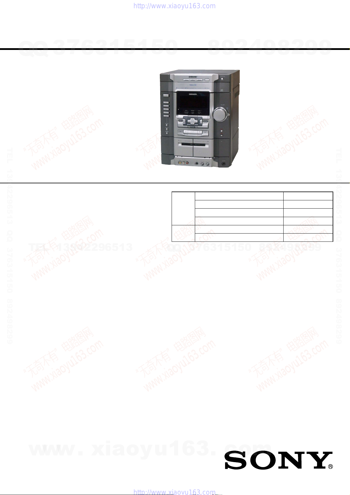
HCD-RV7/R V8 are the amplifier, video CD/CD pla yer ,
tape player and tuner section in MHC-RV7/RV8.
Photo: HCD-RV8
Model Name Using Similar Mechanism NEW
CD
Section
TAPE
Section
CD Mechanism Type CDM58E-30BD62
Base Unit Name BU-30BD62
Optical Pick-up Name A-MAX.3
Model Name Using Similar Mechanism NEW
Tape T ransport Mechanism T ype TCM-230AWR41CS
8
9
2
4
9
8
2
9
E Model
9
TEL 13942296513 QQ 376315150 892498299
TEL
13942296513
Amplifier section
Saudi Arabian Models
The following are measured at AC 127, 220, 240V,
50/60 Hz
DIN power output (rated) 160 + 160 watts
Continuous RMS power output (reference)
Other Models
The following are measured at AC 120, 220, 240V
50/60 Hz
DIN power output (rated) 160 + 160 watts
Continuous RMS power output (reference)
Inputs
GAME (VIDEO): 1 Vp-p, 75 ohms
(phono jack)
GAME (AUDIO): Voltage 250 mV,
(phono jacks) impedance 47 kilohms
MD/VIDEO (AUDIO) IN: voltage 450 mV/250 mV,
(phono jacks) impedance 47 kilohms
MIC: sensitivity 1 mV,
(phone jack) impedance 10 kilohms
(6 ohms at 1 kHz, DIN)
210 + 210 watts (HCD-RV8)
200 + 200 watts (HCD-RV7)
(6 ohms at 1 kHz,
10% THD)
(6 ohms at 1 kHz, DIN)
210 + 210 watts (HCD-RV8)
200 + 200 watts (HCD-RV7)
(6 ohms at 1 kHz,
10% THD)
5
1
3
6
7
3
Q
Q
SPECIFICATIONS
Outputs
VIDEO OUT: max. output level 1 Vp-p,
(phono jacks) unbalanced, Sync.
AUDIO OUT: Voltage 250 mV
(phono jacks) impedance 47 kilohms
PHONES: accepts headphones of
(stereo mini jack) 8 ohms or more
FRONT SPEAKER: accepts impedance of 6 to
SURROUND SPEAKER: accepts impedance of
SUBWOOFER:
(RV8)
VIDEO CD/CD player section
System Compact disc and digital
Laser Semiconductor laser
Frequency response 2 Hz – 20 kHz (±0.5 dB)
Wave length 795 nm
Video color system format NTSC, PAL
Tape player section
Recording system 4-track 2-channel stereo
Frequency response 50 – 13,000 Hz (±3 dB),
negative load impedance
75 ohms
16 ohms
24 ohms or more
accept impedance of
8 ohms or more
audio system
(λ=795nm)
using Sony TYPE I
cassette
2
8
9
4
2
9
8
0
5
1
Tuner section
FM stereo, FM/AM superheterodyne tuner
FM tuner section
Tuning range 87.5 – 108.0 MHz
Antenna FM lead antenna
Antenna terminals 75 ohm unbalanced
Intermediate frequency 10.7 MHz
AM tuner section
Tuning range
Latin American models:
Saudi Arabian models: 531 – 1,602 kHz
Other models: 531 – 1,602 kHz
Antenna AM loop antenna
Antenna terminals External antenna terminal
Intermediate frequency 450 kHz
530 – 1,710 kHz
(with the interval set at 10
kHz)
531 – 1,710 kHz
(with the interval set at 9
kHz)
(with the interval set at 9
kHz)
(with the interval set at 9
kHz)
530 – 1,710 kHz
(with the interval set at 10
kHz)
– Continued on next page –
9
9
w
w
w
9-874-091-01 Sony Corporation
2002G0500-1 Home Audio Company
C 2002.07 Published by Sony Engineering Corporation
.
xia
o
y
u
1
COMPACT DISC DECK RECEIVER
6
3
.
c
o
m
HCD-RV7/RV8
General
Power requirements
Thailand models: 220 V AC, 50/60 Hz
Q
Q
Saudi Arabian models: 120 – 127 V, 220 V or
Other models: 120 V, 220 V or 230 – 240
Power consumption 300 watts (HCD-RV8)
Dimensions (w/h/d) Approx. 280 x 360 x 445
Mass :
Design and specifications are subject to change
without notice.
TEL 13942296513 QQ 376315150 892498299
7
3
6
230 – 240 V AC, 50/60
Hz
Adjustable with voltage
selector
V AC, 50/60 Hz
Adjustable with voltage
selector
240 watts (HCD-RV7)
mm
Approx. 13.1 kg (HCD-RV8)
Approx. 11.0 kg (HCD-RV7)
3
1
5
1
5
Notes on chip component replacement
•Never reuse a disconnected chip component.
0
• Notice that the minus side of a tantalum capacitor may be damaged by heat.
Flexible Circuit Board Repairing
•Keep the temperature of the soldering iron around 270 ˚C during repairing.
• Do not touch the soldering iron on the same conductor of the
circuit board (within 3 times).
• Be careful not to apply force on the conductor when soldering
or unsoldering.
CAUTION
Use of controls or adjustments or performance of procedures
other than those specified herein may result in hazardous radiation exposure.
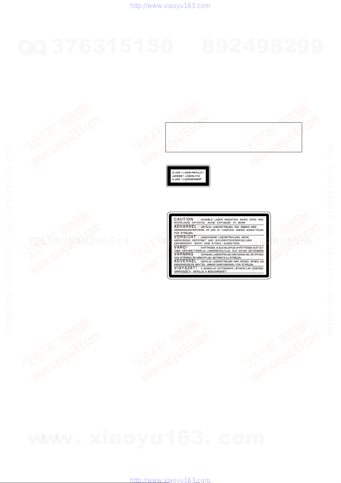
The following caution label is located inside the unit.
4
2
9
8
This appliance is classified as
a CLASS 1 LASER product.
The CLASS 1 LASER
PRODUCT MARKING is
located on the rear exterior.
9
8
2
9
9
TEL 13942296513 QQ 376315150 892498299
TEL
13942296513
Q
Q
3
7
6
3
1
5
1
5
0
8
9
2
4
9
8
2
9
9
2
w
w
w
.
xia
SAFETY-RELATED COMPONENT WARNING!!
COMPONENTS IDENTIFIED BY MARK 0 OR DOTTED
LINE WITH MARK 0 ON THE SCHEMATIC DIA GRAMS
AND IN THE PARTS LIST ARE CRITICAL TO SAFE
o
y
u
OPERATION. REPLACE THESE COMPONENTS WITH
1
6
SONY PARTS WHOSE PART NUMBERS APPEAR AS
SHOWN IN THIS MANUAL OR IN SUPPLEMENTS PUBLISHED BY SONY.
3
.
c
o
m

TABLE OF CONTENTS
7
Q
Q
TEL 13942296513 QQ 376315150 892498299
3
1. SERVICING NOTES ................................................ 4
2. GENERAL
Location of Controls ....................................................... 5
Setting the Clock............................................................. 6
3. DISASSEMBLY
3-1. Disassembly Flow ........................................................... 7
3-2. Top Case .......................................................................... 8
3-3. Loading Panel.................................................................. 8
3-4. CD Mechanism Deck (CDM58E-30BD62) ................... 9
3-5. Front Panel Section ......................................................... 9
3-6. Back Panel Section.......................................................... 10
3-7. MAIN Board ................................................................... 10
3-8. BU-30 (61) Assy ............................................................. 11
3-9. DRIVER Board, MOTOR Board,
SENSOR (CD) Board and VIDEO Board...................... 11
3-10. Tape Mechanism Deck (TCM-230AWR41CS).............. 12
3-11. Belt .................................................................................. 12
3-12. SW Board, HEAD (A) Board and HEAD (B) Board..... 13
4. TEST MODE.............................................................. 14
6
3
1
5
1
5
0
7-27. Printed Wiring Boards
7-28. Schematic Diagram
7-29. Printed Wiring Boards
7-30. Schematic Diagram
7-31. Printed Wiring Boards
7-32. Schematic Diagram
7-33. IC Pin Function Description ........................................... 56
8. EXPLODED VIEWS
8-1. Panel Section ................................................................... 65
8-2. Front Panel Section ......................................................... 66
8-3. Chassis Section ............................................................... 67
8-4. CD Mechanism Deck Section (CDM58E-30BD62) ...... 68
8-5. Base Unit Section (BU-30BD62) ................................... 69
8-6. Tape Mechanism Deck Section
HCD-RV7/RV8
4
2
9
8
– PANEL/CD OPEN/CD SWITCH Boards – ................ 48
– PANEL/CD OPEN/CD SWITCH Boards – ................ 49
– PAD SWITCH/VOL Boards –..................................... 50
– PAD SWITCH/VOL Boards –..................................... 51
– MAIN TRANS/SUB-TRANS Boards –...................... 52
– MAIN TRANS/SUB-TRANS Boards –...................... 53
(TCM-230AWR41CS) .................................................... 70
9
8
2
9
9
TEL 13942296513 QQ 376315150 892498299
5. MECHANICAL ADJUSTMENTS....................... 18
6. ELECTRICAL ADJUSTMENTS
Deck section .................................................................... 18
CD Section ...................................................................... 21
VIDEO Section ............................................................... 21
TEL
w
13942296513
7. DIAGRAMS
7-1. Block Diagram – CD SERVO Section – ....................... 22
7-2. Block Diagram – AUDIO/VIDEO CD Section –.......... 23
7-3. Block Diagram – TUNER/TAPE DECK Section – ...... 24
7-4. Block Diagram – MAIN Section – ................................ 25
7-5. Block Diagram – DISPLAY/KEY CONTROL/
POWER SUPPLY Section – ........................................... 26
7-6. Note for Printed Wiring Boards and
Schematic Diagrams ....................................................... 27
7-7. Printed Wiring Board – BD Board – ............................. 28
7-8. Schematic Diagram – BD Board – ................................ 29
7-9. Schematic Diagram – VIDEO Board (1/2) – ................ 30
7-10. Schematic Diagram – VIDEO Board (2/2) – ................ 31
7-11. Printed Wiring Board – VIDEO Board – ....................... 32
7-12. Printed Wiring Boards
– DRIVER/MOTOR/SENSOR (CD) Boards –.............. 33
7-13. Schematic Diagram
– DRIVER/MOTOR/SENSOR (CD) Boards –.............. 33
7-14. Printed Wiring Boards
– SW/HEAD (A)/HEAD (B) Boards – .......................... 34
7-15. Schematic Diagram – SW Board –................................ 35
7-16. Printed Wiring Board – MAIN Board – ........................ 37
7-17. Schematic Diagram – MAIN Board (1/4) – .................. 38
7-18. Schematic Diagram – MAIN Board (2/4) – .................. 39
7-19. Schematic Diagram
– MAIN (3/4)/HEAD (A)/HEAD (B) Boards –............. 40
7-20. Schematic Diagram – MAIN Board (4/4) – .................. 41
7-21. Printed Wiring Board – GAME IN Board – .................. 42
7-22. Schematic Diagram – GAME IN Board –..................... 43
7-23. Printed Wiring Board – SUB WOOFER Board – ......... 44
7-24. Schematic Diagram – SUB WOOFER Board – ............ 45
7-25. Printed Wiring Boards
w
w
– POWER/SENSOR Boards –........................................ 46
7-26. Schematic Diagram
– POWER/SENSOR Boards –........................................ 47
.
xia
o
y
u
Q
Q
1
9. ELECTRICAL PARTS LIST ............................... 71
2
8
9
4
2
9
8
0
5
1
5
1
3
6
7
3
6
3
.
c
o
m
9
9
3
HCD-RV7/RV8
SECTION 1
SERVICING NOTES
NOTES ON HANDLING THE OPTICAL PICK-UP
BLOCK OR BASE UNIT
Q
Q
The laser diode in the optical pick-up block may suffer electrostatic break-down because of the potential difference generated
by the charged electrostatic load, etc. on clothing and the human
body.
During repair, pay attention to electrostatic break-down and also
use the procedure in the printed matter which is included in the
repair parts.
The flexible board is easily damaged and should be handled with
care.
NOTES ON LASER DIODE EMISSION CHECK
The laser beam on this model is concentrated so as to be focused
on the disc reflective surface by the objective lens in the optical
TEL 13942296513 QQ 376315150 892498299
pick-up block. Therefore, when checking the laser diode emission, observe from more than 30 cm away from the objectiv e lens.
LASER DIODE AND FOCUS SEARCH OPERATION
CHECK
Carry out the “S curve check” in “CD section adjustment” and
check that the S curve waveforms is output three times.
TEL
7
3
13942296513
6
3
1
5
1
5
• MODEL IDENTIFICATION
– Back Panel –
0
RV7: E, Singapore and Malaysia
models
RV8: E, Singapore and Malaysia
models
RV7: Thai model 4-237-780-8[]
RV7: Saudi Arabia model 4-239-663-6[]
Q
Q
RV8: Saudi Arabia model 4-239-663-7[]
3
7
4
2
9
8
PART No.
MODEL PART No.
8
0
5
1
5
1
3
6
8
9
4-237-780-3
4-237-780-4[]
4
2
9
9
2
[]
8
9
2
9
9
TEL 13942296513 QQ 376315150 892498299
9
4
w
w
w
.
xia
o
y
u
1
6
3
.
c
o
m
w
waw
SECTION 2
GENERAL
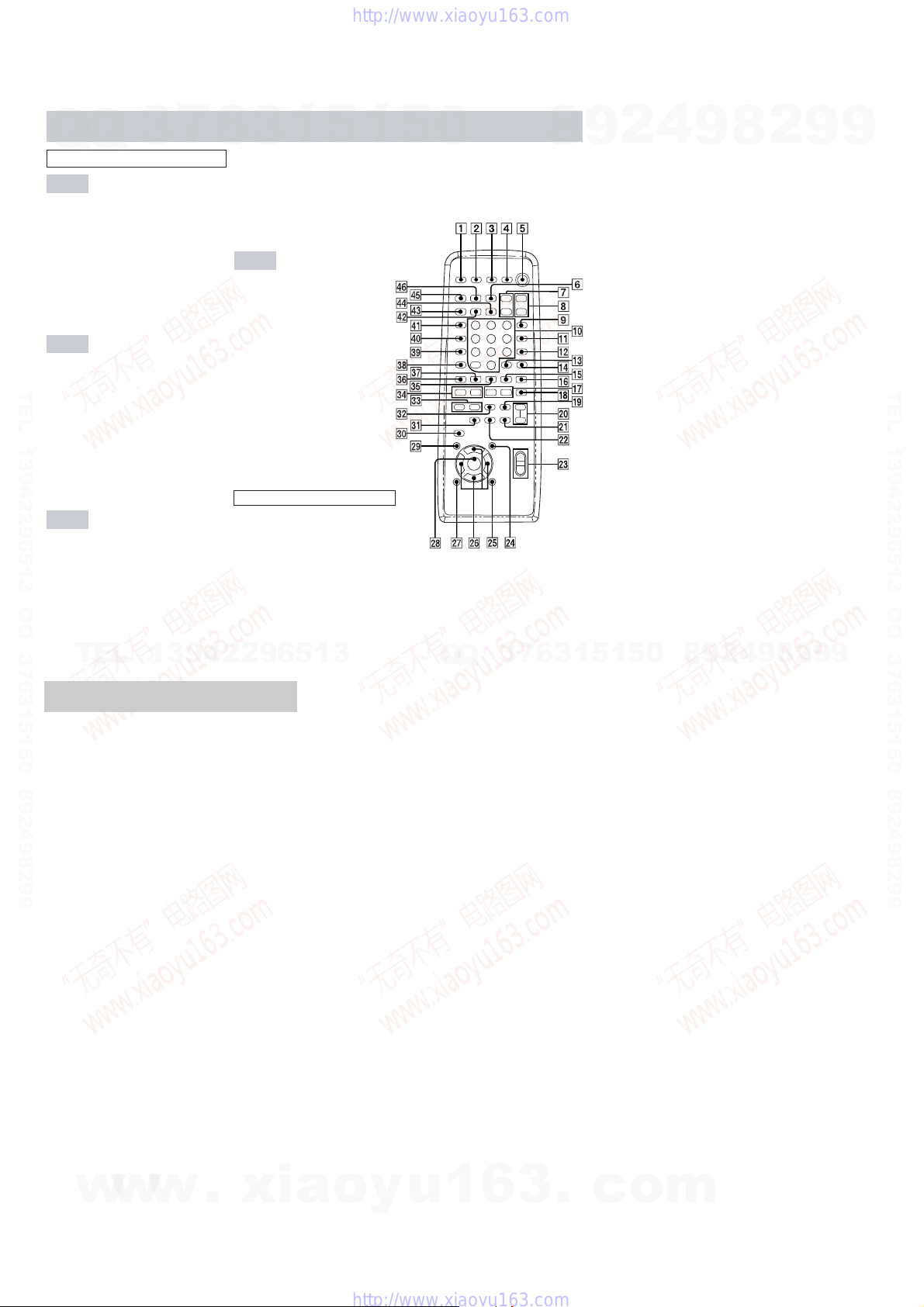
LOCATION OF CONTROLS
7
Q
Q
TEL 13942296513 QQ 376315150 892498299
3
– Front Panel –
6
ALPHABETICAL ORDER
A - D
ALBUM + ql
ALBUM – wh
CD ek
CD SYNC HI-DUB qg
CINEMA SPACE rs
DECK A A wl
DECK B A qj
DIMMER 9
DIRECTION q;
DISC 1~3 4
DISC SKIP EX-CHANGE 5
Disc tray 3
DISPLAY 7
E - J
ECHO LEVEL wa
EDIT q;
EFFECT ON/OFF rh
ENTER rf
3
1
1
5
2
1
3
5
0
FM MODE qd
GAME ef
GAME EQ rj
GAME INPUT (jacks) wg
GAME MIXING es
GROOVE rk
IR (receptor) 2
K - Q
KARAOKE PON ea
MD (VIDEO) eg
MIC jack wd
MIC LEVEL ws
MOVIE EQ ra
MUSIC EQ el
OPEN/CLOSE Z 6
P FILE rd
PHONES (jack) w;
PLAY MODE ed
PICTURE EFFECT rg
4
5
6
8
This section is extracted from
instruction manual.
4
2
9
R - Z
REC PAUSE/START qh
REPEAT qd
SPECTRUM 8
SHUTTLE qa
SURROUND SPEAKER MODE
e;
TAPE A/B eh
TUNER/BAND ej
TUNER MEMORY ed
VOLUME qs
BUTTON DESCRIPTIONS
@/1 1
hH wf
x qf
X wj
> qk
. wk
M/+ ql
m/– wh
v/V/b/B r;
9
HCD-RV7/RV8
2
8
9
9
TEL 13942296513 QQ 376315150 892498299
TEL
ek
13942296513
eh
ef
ej
eg
ed
es
ea
e;
wl
wk
wj
wh
wg
X
W
s
Q
Q
3
;
7
6
7
9
L
M
N
qh
qj
qk
ql
3
8
0
K
O
1
5
rk
1
el
5
0
r;
8
rf
9
r
a
2
d
r
4
rs
9
8
2
9
9
w
w
w
.
xia
o
y
u
1
6
3
.
c
o
m
5
HCD-RV7/RV8
Remote Control
Q
Q
ALPHABETICAL ORDER
A - D
ALBUM +/– ed
CD rg
CINEMA SPACE ws
CLEAR qf
CLOCK/TIMER SELECT 2
CLOCK/TIMER SET 3
D.SKIP qa
DIMMER el
DISPLAY ra
E - M
EFFECT ON/OFF wa
ENTER wk
TEL 13942296513 QQ 376315150 892498299
GAME rs
GAME EQ wj
GAME MIXING rd
KARAOKE PON ql
KEY CONTROL #/2 w;
MD (VIDEO) rf
MOVIE EQ wf
MUSIC EQ wl
N - R
NEXT ej
Numeric buttons q;
ON SCREEN qd
P FILE wg
PICTURE EFFECT ea
3
7
1
6
3
PLAY MODE es
PRESET +/– ef
PREV eh
REPEAT qs
RETURN O eg
S - Z
SELECT qg
SLEEP 1
SPECIAL MENU ek
SPECTRUM r;
SURROUND SPEAKER MODE
e;
TAPE A/B 6
TUNER/BAND rh
TUNING +/– qj
TV CH +/– 8
TV @/1 4
TV VOL +/– 7
TV/VIDEO 9
VOL +/– wd
BUTTON DESCRIPTIONS
@/1 5
nN qg
X qh
x qk
./> ef
m/M qj
v/V/b/B wh
5
1
5
0
.
–
123
456
789
.
m
v
v
+–+
m
3
2
+
–
8
9
2
4
9
8
2
9
9
TEL 13942296513 QQ 376315150 892498299
TEL
Setting the clock
1
Turn on the system.
2
Press CLOCK/TIMER SET on the
remote.
When you set the time for the first time,
proceed to step 5.
3
Press V or v repeatedly to select
CLOCK SET.
4
Press ENTER.
5
Press V or v repeatedly to set the hour.
6
Press ENTER.
7
Press V or v repeatedly to set the
minute.
8
Press ENTER.
The clock starts functioning.
Tip
If you have made a mistake or want to change the
time, start over from step 2.
Note
The clock settings are canceled when you disconnect
the power cord or if a power failure occurs.
13942296513
Q
Q
3
7
6
3
1
5
1
5
0
8
9
2
4
9
8
2
9
9
6
w
w
w
.
xia
o
y
u
1
6
3
.
c
o
m
SECTION 3
DISASSEMBLY
• This set can be disassembled in the order shown below.
7
Q
Q
TEL 13942296513 QQ 376315150 892498299
3
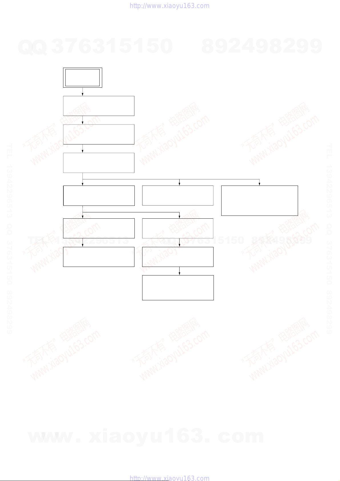
3-1. DISASSEMBLY FLOW
6
SET
3-2. TOP CASE
(Page 8)
3-3. LOADING PANEL
(Page 8)
3-4. CD MECHANISM DECK
(CDM58E-30BD62)
(Page 9)
3
1
5
1
5
0
8
9
2
4
9
HCD-RV7/RV8
2
8
9
9
TEL 13942296513 QQ 376315150 892498299
TEL
3-5. FRONT PANEL SECTION
(Page 9)
3-6. BACK PANEL SECTION
(Page 10)
13942296513
3-7. MAIN BOARD
(Page 10)
3-8. BU-30 (61) ASSY
(Page 11)
3-10.TAPE MECHANISM DECK
(TCM-230AWR41CS)
(Page 12)
3
6
7
3
Q
Q
3-11.BELT
(Page 12)
3-12.SW BOARD,
HEAD (A) BOARD AND
HEAD (B) BOARD
(Page 13)
3-9. DRIVER BOARD,
MOTOR BOARD,
SENSOR (CD) BOARD AND
VIDEO BOARD
(Page 11)
0
5
1
5
1
8
9
2
4
9
8
2
9
9
w
w
w
.
xia
o
y
u
1
6
3
.
c
o
m
7
)
HCD-RV7/RV8
Note: Follow the disassembly procedure in the numerical order given.
Q
Q
3-2. TOP CASE
6
side panel (L)
3
two screws (case 3 TP2)
4
7
6
3
1
9
5
top
case
5
(BVTP 3
8
1
two screws
5
×
10)
0
8
9
8
2
4
7
two screws
(BVTP 3
9
×
8
12)
2
9
9
TEL 13942296513 QQ 376315150 892498299
4
screw (case 3TP2)
TEL
3-3. LOADING PANEL
13942296513
3
four claws
Q
Q
3
7
6
3
1
5
3
side panel (R)
0
5
1
2
two
screws
(BVTP 3
2
9
8
1
three screws (case 3 TP2
4
9
×
8
10)
2
9
TEL 13942296513 QQ 376315150 892498299
9
2
Pull-out the disc table.
w
w
8
4
loading panel
w
.
xia
o
y
u
1
6
3
–BOTTOM VIEW–
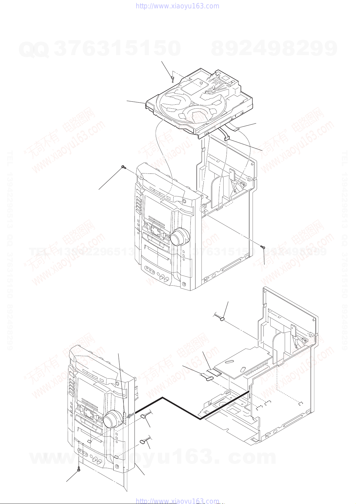
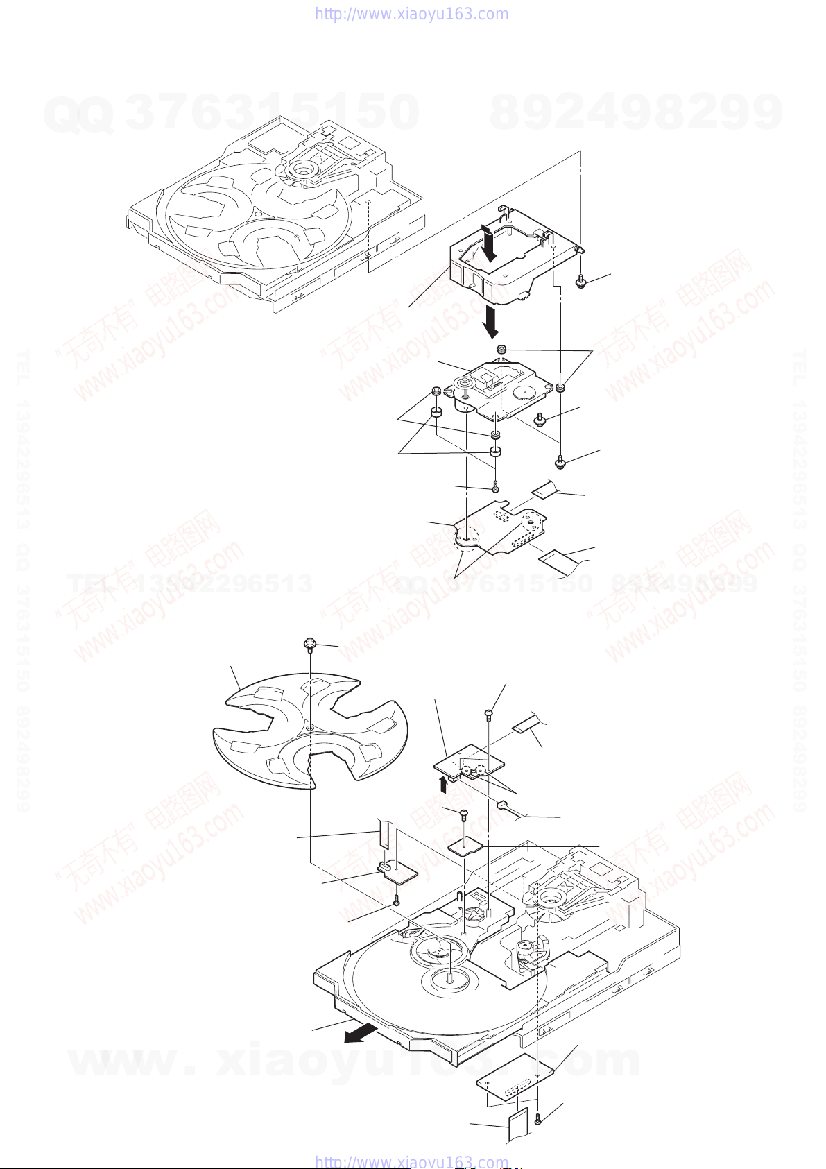
CD mechanism deck (CDM58E-30BD62)
1
Turn the pulley in the direction of the arrow.
Front panel side
.
c
o
m
)
Q
3-4. CD MECHANISM DECK (CDM58E-30BD62)
2
Q
3
7
6
5
CD mechanism deck (CDM58E-30BD62)
3
1
5
connector
1
(
CN301)
5
0
8
9
2
4
9
1
wire (flat type)
(19 core)
HCD-RV7/RV8
2
8
(CN201
9
9
TEL 13942296513 QQ 376315150 892498299
3
screw
(BVTP 3
× 10)
TEL
13942296513
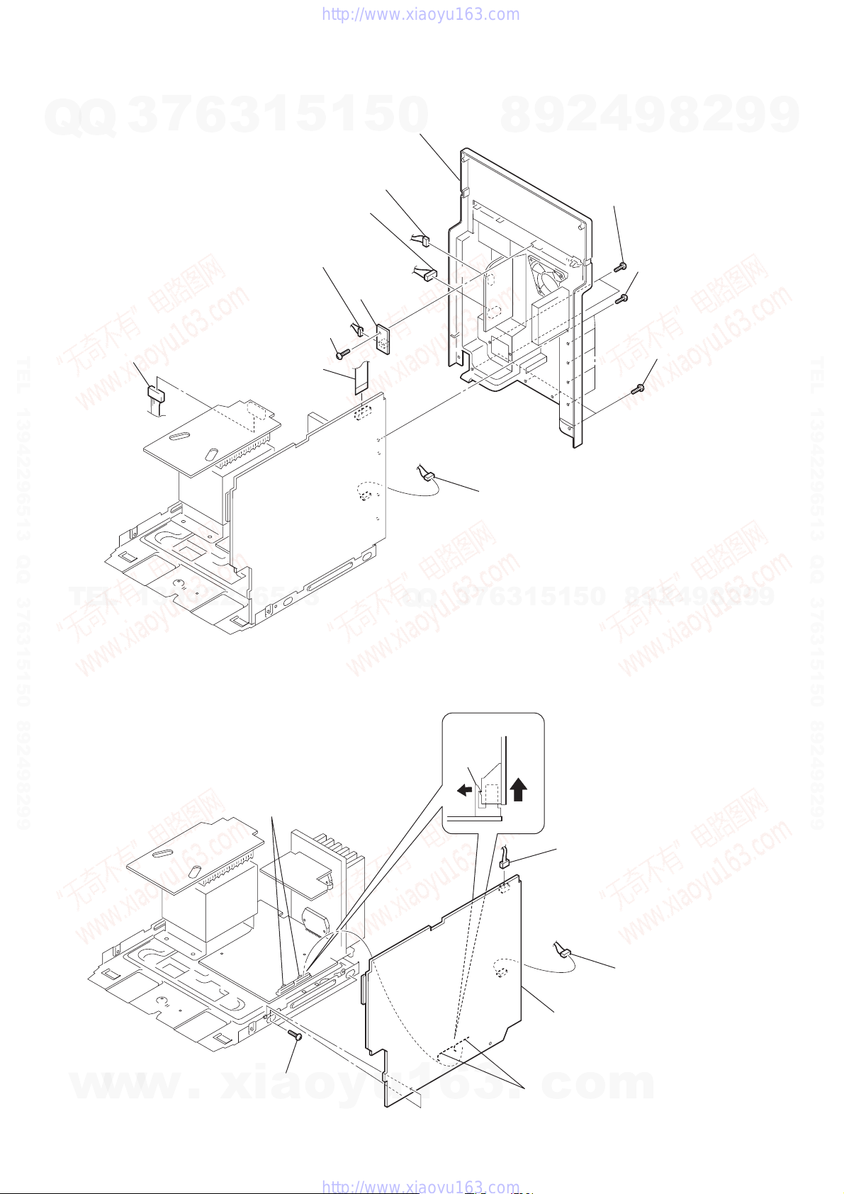
3-5. FRONT PANEL SECTION
Q
Q
3
7
6
3
1
1
5
2
connector
CN783)
(
5
0
2
8
3
connector
(
CN202)
2
9
screw
(BVTP 3
4
× 10)
9
8
2
9
TEL 13942296513 QQ 376315150 892498299
9
w
w
w
3
four
(BVTP 3
.
screws
× 10
4
xia
)
1
connector
CN401)
(
2
connector
CN781)
(
2
connector (
2
connector (
o
y
u
5
front panel section
1
CN1)
CN2)
6
wire (flat type)
(17 core)
3
(CN304)
.
c
o
m
9
)
)
HCD-RV7/RV8
3-6. BACK PANEL SECTION
7
7
Q
Q
TEL 13942296513 QQ 376315150 892498299
5
connector (CN973)
3
6
1
wire
(CN702)
1
5
5
connector
4
screw
5
connector
connector
×
3
2
(BVTP 3
(flat type) (11core)
1
(CN974)
10)
5
(CN976)
(CN701)
3
sensor board
back panel section
0
8
9
2
4
9
6
two
(BVTP 3
6
(BVTP 3
8
screws
×
10)
five
screws
6
four
(BVTP 3
2
×
10)
screws
×
9
10
9
TEL 13942296513 QQ 376315150 892498299
TEL
3-7. MAIN BOARD
13942296513
4
two
claws
Q
Q
7
3
main board
claw
5
connector
3
6
1
(CN891)
1
5
0
5
3
connector
(HCD-RV8)
9
8
(CN904)
2
4
9
8
2
9
9
10
w
w
w
.
xia
1
two screws
o
(BVTP 3
y
u
1
6
3
×
10)
.
5
main board
2
two
connectors
c
o
(CN502, CN503)
3
connector
(HCD-RV8)
m
(CN903
)
3-8. BU-30 (61) ASSY
7
Q
Q
TEL 13942296513 QQ 376315150 892498299
3
6
3
1
5
1
qf
holder (BU) (BU-30) assy
0
two insulators (BU-30)
5
0
qa
BU-30 (61) assy
8
qd
9
9
2
4
0
two insulators (BU-30)
8
screws (DIA. 12)
8
9
qs
screw (PTPWH M2.6)
HCD-RV7/RV8
2
9
9
TEL 13942296513 QQ 376315150 892498299
6
two stoppers (BU)
5
two screws (BVTP 2.6
4
BD board
3
TEL
13942296513
3-9. DRIVER BOARD, MOTOR BOARD, SENSOR (CD) BOARD AND VIDEO BOARD
qg
tray
qh
screw (BVTP 2.6
5
wire (flat type) (8 core)
(CN702)
Remove the four solders of
sled motor and spindle motors.
qf
screw (PTPWH 2.6
Q
Q
qd
×
8)
7
3
×
8)
motor board
0
×
8)
1
5
1
3
6
9
two screws (BVTP 2.6
qa
wire (flat type) (8 core)
(CN721)
8
Remove the two solderings of motor.
0
5
qs
connector
2
wire (flat type) (16 core)
(CN102)
1
×
qj
7
two
screws (PTPWH M2.6
wire (flat type) (28 core)
(CN101)
8
9
4
2
9
8
8)
(CN722)
sensor (CD)
board
2
9
9
w
w
w
7
driver board
6
s
crew (BVTP 2.6
4
Pull out the disc table.
.
xia
×
8)
o
y
u
1
6
3
1
wire (flat type) (28 core)
(CN101)
.
c
3
o
2
two s
(BVTP 2.6
video board
m
crews
×
8)
11
)
)
HCD-RV7/RV8
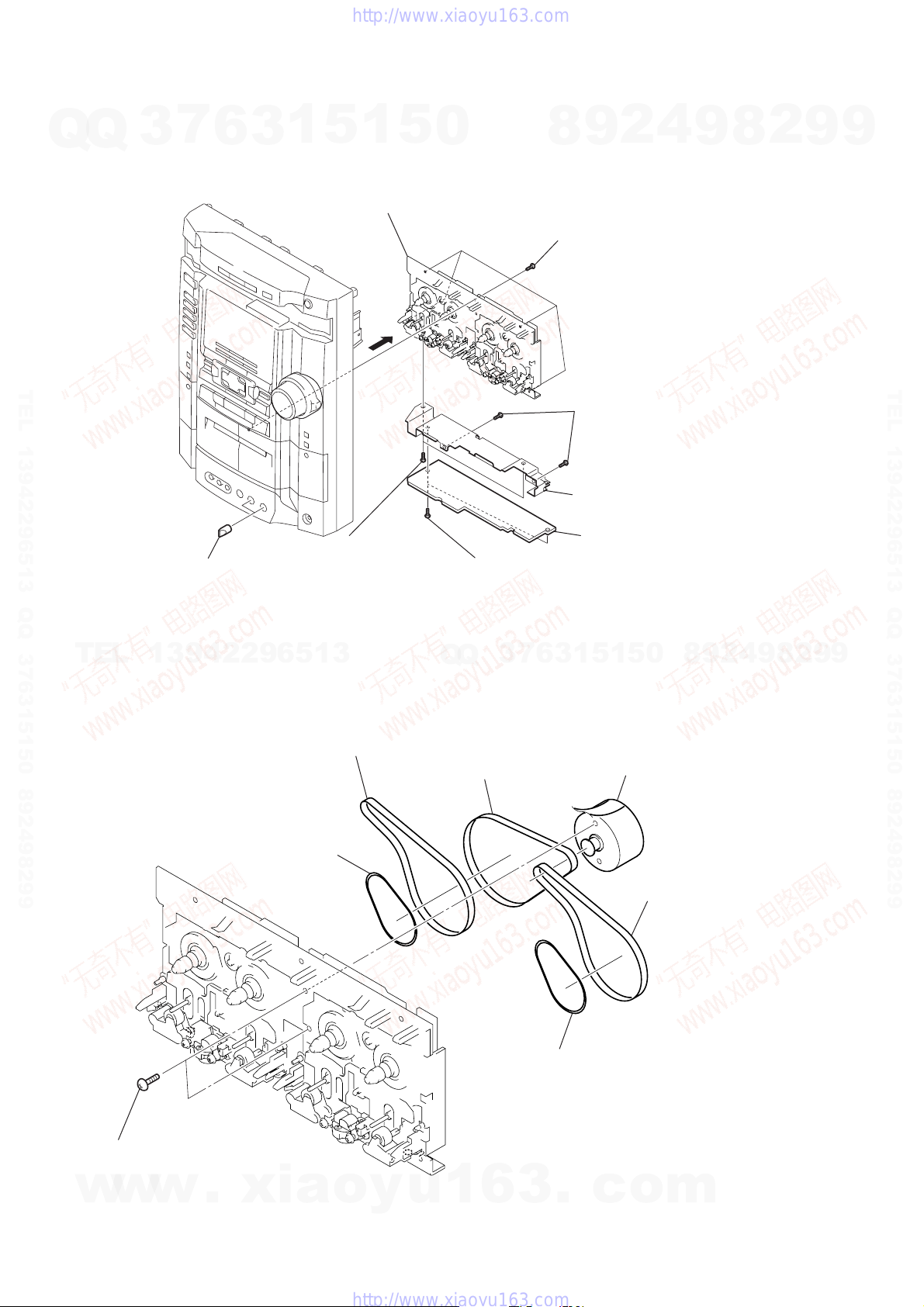
3-10. TAPE MECHANISM DECK (TCM-230AWR41CS)
Q
Q
3
7
6
3
1
5
1
5
8
tape mechanism deck
(TCM-230AWR41CS)
3
0
9
8
2
five
screws
(BVTP 2.6
2
×
8)
4
9
8
2
9
9
TEL 13942296513 QQ 376315150 892498299
6
two
screws
TEL
3-11. BELT
1
two
knobs (mic)
(P 2.6
13942296513
4
×
3)
belt
(capstan B)
Q
Q
4
two
screws
(BVTP 2.6
7
3
3
belt
(capstan C)
6
×
3
2
two
(BVTP 2.6
7
shield plate (TC
5
game in board
8)
1
5
1
screws
5
2
motor assy
(M901)
×
0
8)
9
8
(capstan
2
4
9
8
2
9
TEL 13942296513 QQ 376315150 892498299
9
12
1
(PS 2.6
w
w
two
screws
×
5)
w
.
xia
5
belt
(FR)
o
y
u
1
6
3
5
.
belt
(FR)
c
4
o
belt
(capstan B)
m
Q
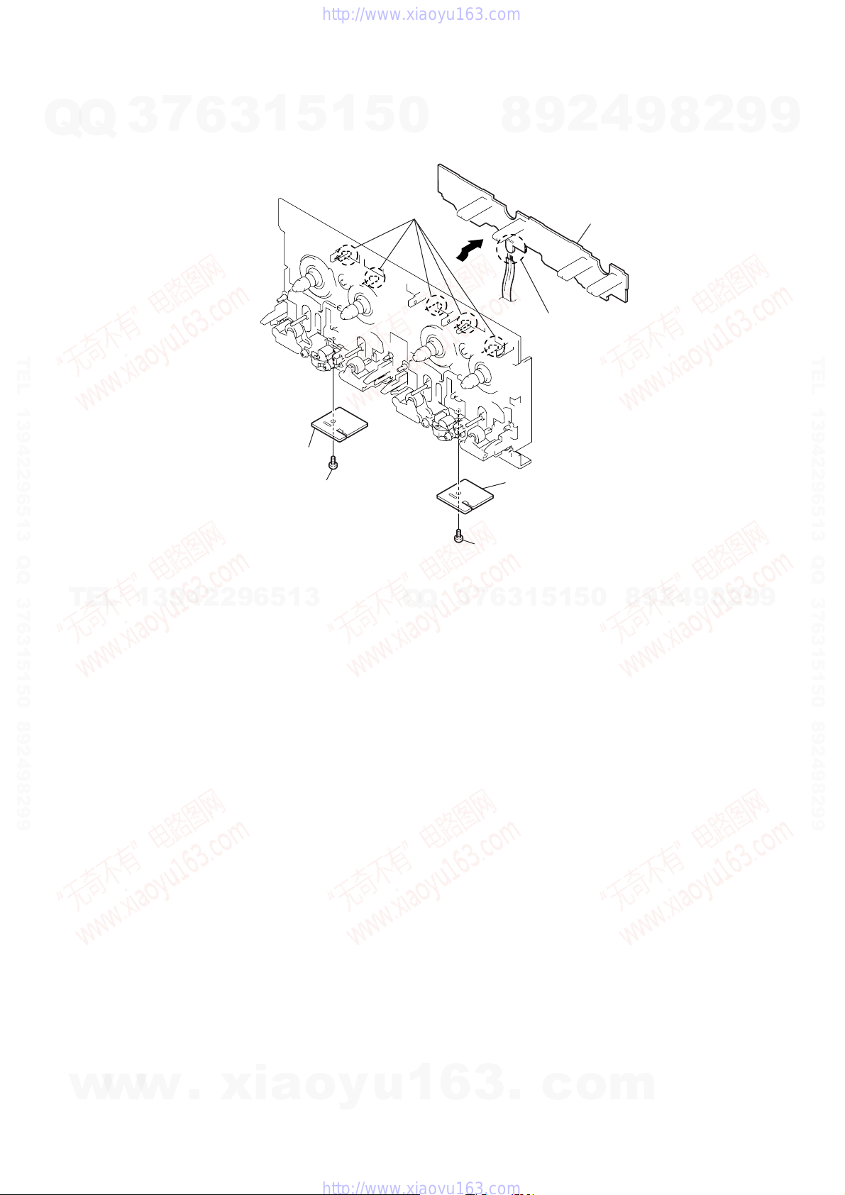
3-12. SW BOARD, HEAD (A) BOARD AND HEAD (B) BOARD
Q
3
7
6
3
1
5
1
5
2
five claws
0
8
4
2
9
3
SW board
1
Remove the four solders.
9
HCD-RV7/RV8
2
8
9
9
TEL 13942296513 QQ 376315150 892498299
5
head (A) board
4
TEL
screw (PTT 2
13942296513
×
Q
4)
Q
3
6
7
7
head (B) board
screw (PTT 2
5
1
3
6
×
1
4)
5
0
8
9
2
4
9
8
2
9
TEL 13942296513 QQ 376315150 892498299
9
w
w
w
.
xia
o
y
u
1
6
3
.
c
o
m
13
HCD-RV7/RV8
SECTION 4
TEST MODE
[GC TEST MODE]
• This mode is used to check the fluorescent indicator tube, LED,
Q
Q
model, destination software version, volume, key and VACS
level.
Procedure:
1. Press three b uttons x , [ENTER], and [DISC 2] simultaneously.
2. LEDs and fluorescent indicator tube are all turned on.
3. When you want to enter the software version display mode,
press [DISC 1]. The model and destination are displayed.
4. Each time [DISC 1] is pressed, the display changes starting
from MC version, GC version, CD version, CDDM version,
CDMA version, CDMB version, BDA version, BDB version,
ST version, T A version, TM version and TC version in this order ,
and returns to the MC version display.
5. When [DISC 3] is pressed while the version numbers are being
TEL 13942296513 QQ 376315150 892498299
displayed except model and destination, year, month and day of
the software creation appear. When [DISC 3] is pressed again, the
display returns to the software version display . When [DISC 1] is
pressed while year, month and day of the software creation are
being displayed, the year, month and day of creation of the software
versions are displayed in the same order of version display.
6. Press [DISC 2] button, and the key check mode is activated.
7. In the key check mode, the fluorescent indicator tube displays
“K0 V0”. Each time a button is pressed, “K” value increases.
However, once a button is pressed, it is no longer taken into
account.
“V” value increases like 1, 2, 3 ... if rotating [VOLUME] knob
in “+” direction, or it decreases like 0, 9, 8 ... if rotating in
“–” direction.
8. Also when [DISC 3] is pressed after lighting of all LEDs and
fluorescent indicator tubes, value of VACS level appears.
9. To release this mode, press three buttons in the same manner as
step 1, or disconnect the power cord.
TEL
[MC TEST MODE]
•This mode is used to check operations of the respective sections
of Amplifier, Tuner , and Tape.
Procedure:
* To enter MC Test Mode
1. Press three buttons of x , [ENTER] and [DISC 3] simultaneously.
2. The messages MUSIC, MOVIE, GAME and P FILE flash on
the fluorescent indicator tube.
The input FUNCTION is changed to VIDEO.
3
7
6
3
1
13942296513
5
1
5
* T ape function
1. When a tape is inserted in tape deck B and recording is started,
0
the input source function selects VIDEO automatically.
[CD SYNC HI-DUB] button is pressed during recording
When
in function, ALC is turned on.
2. When x button is pressed to stop recording, the tape deck B is
selected and tape is rewound, tape is rew ound using – m button,
tape is stops at around the record-starting position and playback
of the recorded portion of the tape is started. If the [REC PAUSE/
START] button is pressed for a pause and pressed again to resume
recording, when tape deck B is rewound, tape deck B will be
rewound until the position where the pause is applied.
3. When [CD SYNC HI-DUB] button is pressed during playback
of tape deck B, either normal speed or high speed can be selected
by this button.
* AMS Test Mode
1. Select the function “TAPE A” or “TAPE B”.
2. Select the loop and relay by pressing the [DIRECTION] button.
Insert a test tape AMS-110A or AMS-120 to selected tape deck.
3. Press the [SPECTRUM] button to enter the AMS test mode.
4. After a tape is rewound first, the FF AMS is checked, and the
mechanism is shut off after detecting the AMS signal twice.
5. Then the REW AMS is checked and the mechanism is shut off
after detecting the AMS signal twice.
6. When the check is complete, a message of either OK or NG
appears.
* To release MC Test mode.
1. To release this mode, press the ?/1 button.
2. The cold reset is enforced at the same time.
[COLD RESET]
Q
Q
• The cold reset clears all data including preset data stored in the
RAM to initial conditions. Execute this mode when returning
the set to the customer.
Procedure:
1. Press three buttons x , [ENTER], and ?/1 simultaneously.
2. The fluorescent indicator tube becomes blank instantaneously,
[VACS ON/OFF MODE]
•This mode is used to switch ON and OFF the VACS (Variable
Attenuation Control System).
7
3
and the set is reset.
8
6
3
9
1
5
2
1
5
4
0
9
8
9
8
2
4
2
9
8
9
2
9
9
TEL 13942296513 QQ 376315150 892498299
9
* Check of Amplifier
1. When v button is pressed, GEQ increases to its maximum and
a message “GEQ MAX” appears.
2. When V button is pressed, GEQ decreases to its minimum and
a message “GEQ MIN” appears.
3. When b or B button is pressed, GEQ is set to flat and a
message “GEQ FLAT” appears.
4. When the [VOLUME] knob is turned clockwise even slightly,
the sound volume increases to its maximum and a message
“VOLUME MAX” appears for two seconds, then the display
returns to the original display.
5. When the [VOLUME] knob is turned counter-clockwise even
slightly, the sound volume decreases to its minimum and a
message “VOLUME MIN” appears for two seconds, then the
display returns to the original display.
* Check of clock frequency
1. To check the frequency of clock used to run the time in the unit,
the clock output is available at IC501 pin el (CLOCK-OUT)
on the MAIN board only during MC test mode.
w
w
2. The frequency is 32.768 kHz or so.
14
w
.
xia
o
y
Procedure:
1. Press ?/1 button to turn the set ON.
2. Press the [ENTER] and [GAME MIXING] buttons simultaneously .
The message “VACS OFF” or “VACS ON” appears.
[TUNER STEP CHANGE]
(EXCEPT Saudi Arabia model)
•A step of AM channels can be changed o ver between 9 kHz and
10 kHz.
Procedure:
1. Press ?/1 button to turn the set ON.
2. Select the function “TUNER”, and press [TUNER/BAND]
button to select the BAND “AM”.
3. Press ?/1 button to turn the set OFF.
4. Press [ENTER] and ?/1 buttons simultaneously, and the
display of fluorescent indicator tube changes to “ AM 9k STEP”
or “ AM 10k STEP”, and thus the channel step is c hanged ov er.
u
1
6
3
.
c
o
m
HCD-RV7/RV8
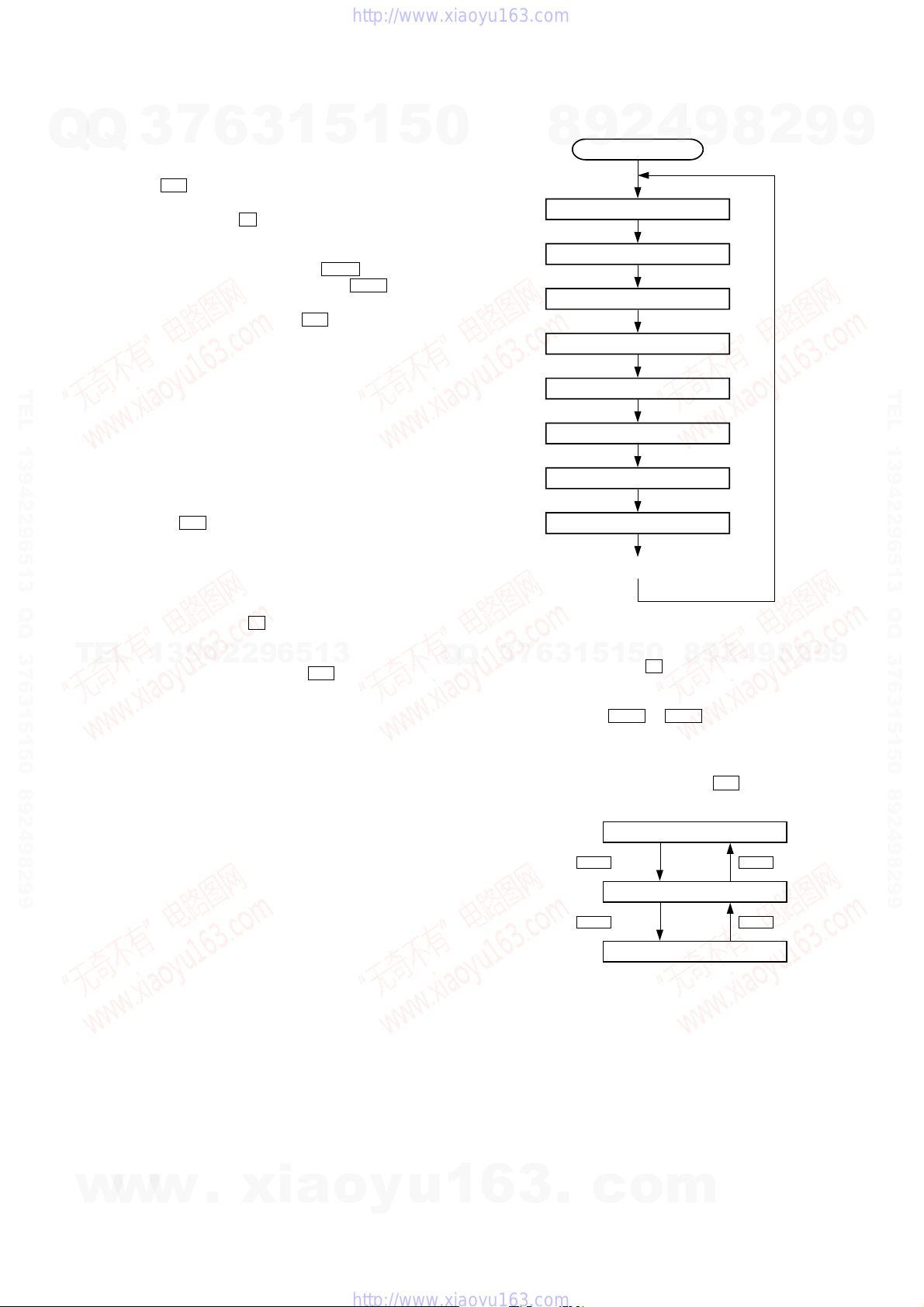
[CD SERVICE MODE]
Q
TEL 13942296513 QQ 376315150 892498299
•This mode can run the CD sled motor freely. Use this mode, for
Q
instance, when cleaning the optical pick-up.
Procedure:
1. Press ?/1 button to turn the set ON.
2. Select the function “CD”.
3. Press three buttons x , [ENTER] , and [OPEN/CLOSE] simultaneously.
4. The CD service mode is selected.
5. With the CD in stop status, press M + button to move the
optical pick-up to outside track, or press – m button to inside
track.
6. To release this mode, press the ?/1 button.
[AGING MODE]
This mode can be used for operation check of CD section and tape
deck section.
CD section and tape deck section work in parallel.
• If an error occurred:
The aging operation stops only an error occurred sections and
display then status.
• If no error occurs:
The aging operation continues repeatedly.
Procedure:
1. Press the ?/1 button to turn the power ON, and press the [CD]
button to select the function “CD”.
2. Set discs on all trays, and set tapes into the decks A and B
respectively.
3. Press the [PLAY MODE] button to set the “ALL DISCS” mode,
and press the [REPEAT] button to “REPEAT” off.
4. Press three buttons of x , [ENTER], and [EX-CHANGE/DISC
SKIP] simultaneously.
5. Aging operations of CD and tape are started at the same time.
TEL
6. To release this mode, press the
power code to turn the power OFF.
1. Display at the Aging Mode
Display operating state of CD section and tape deck section
alternately.
If an error occurred, stop display which that section.
2. CD Section
The sequence during the aging mode is following as below.
Display at the aging mode is the same as the normal operation.
3
7
6
3
1
13942296513
?/1 button or disconnect the
5
1
5
0
Q
Q
Aging mode sequence (CD section) :
• Display at an error occurred (Error display mode)
Procedure:
7
3
1. Press three buttons of
to enter the error display mode.
2. It displays of total error.
3. Each time the
as below.
4. To clear the error record, operate the cold reset. (Refer to the
“MC COLD RESET”)
5. To release this mode, press the ?/1 button or disconnect the
power plug to turn the power OFF.
2
9
8
Start (from disc 1)
Disc chucking
TOC read
Play first track for 2 seconds
Play last track for 2 seconds
EX-change open/close
Open the disc tray
Disc skip
Close the tray
Change the next disc.
0
5
1
5
1
3
6
–
m
x , [ENTER], and [DISC 1] simultaneously
–
m or M
Display of total error
Button
4
2
9
+
2
8
Button
9
9
8
9
4
2
9
8
+
button is pressed, display change
M
9
TEL 13942296513 QQ 376315150 892498299
9
w
w
w
.
xia
o
y
u
1
6
3
.
Display of Mechanical errors
–
m
Button
Display of no disc errors
c
o
m
M
+
Button
15
HCD-RV7/RV8
1) Display of total error
7
Q
Q
EMC**: The number of mechanical error.
EDC**: The number of no disc error after chucking the disc.
2) Display of mechanical errors
TEL 13942296513 QQ 376315150 892498299
M*: The number of mechanical error (“00” is latest one)
(Press the . or > button to changes next error display)
$$: Not used
%%: Loading error (Second figure is not used)
D: The error in the midst of close at the except mechanical
trouble.
E: The error in the midst of open at the except mechanical
trouble.
C: The error in the midst of chucking up at the except
mechanical trouble.
F: The error in the midst of chucking down at the except
mechanical trouble.
&&: Loading error
01: The error in the midst of chucking up.
02: The error in the midst of chucking down.
03: Time-out of EX-open.
TEL
05: Time-out of EX-close.
##: Not used
3) Display of no disc errors
3
13942296513
6
Display
EMC**EDC**
Display
M*$$%%&&##00
Display
D*$$%%&&##00
3
1
5
1
5
3. Tape Deck Section
The sequence during the aging mode is following as below.
0
If an error occurred, stop display that step.
Aging mode sequence (Tape deck section) :
Rewind the tape A and B
FWD play the tape A
Fast forward the tape A
REV play the tape A
Rewind the tape A
FWD play the tape B
7
3
Q
Q
Fast forward the tape B
REV play the tape B
9
8
“TAPE A AG-1”
Shut off
“TAPE A AG-2”
2 minutes
“TAPE A AG-3”
Shut off or 20 seconds
“TAPE A AG-4”
2 minutes
“TAPE A AG-5”
Shut off
“TAPE B AG-2”
2 minutes
5
1
3
6
“TAPE B AG-3”
Shut off or 20 seconds
“TAPE B AG-4”
2 minutes
2
1
5
4
0
9
8
9
8
2
4
2
9
8
9
2
9
9
TEL 13942296513 QQ 376315150 892498299
9
D*: The number of mechanical error(“00” is latest one)
(Press the
$$: Error type
01: Focus error
02: GFS error
03: Set up error
%%: Not used
&&:
00: No disc judgment without chucking retry.
01: No disc judgment after chucking retry.
##: The state when judged no disc error
01: Stop
02: Set up
03: TOC read
04: Access
05: Play
06: Pause
07: Manual search (Play)
08: Manual search (Pause)
w
16
. or > button to changes next error display)
w
w
.
xia
o
Rewind the tape B
“TAPE B AG-5”
Note: “TAPE * AG-*” is display of each step.
[CD REPEAT 5 LIMIT OFF MODE]
Number of repeat for CD playback is 5 times when the repeat mode
is “REPEA T”. This mode enables CD to repeat playback for limitless
times.
Procedure:
1. Press the ?/1 button to turn the power on, and press the [CD]
button to select the function “CD”.
2. Press three b uttons of x , [REPEAT], and [CD] simultaneously
to enter the CD repeat 5 limit off mode and display “REPEAT
OFF”.
3. To release this mode, operate the cold reset. (Refer to the “MC
COLD RESET”)
y
u
1
6
3
.
Shut off
c
o
m
[CD SHIP MODE (MEMORY CLEAR) ]
Q
TEL 13942296513 QQ 376315150 892498299
•This mode moves the optical pick-up to the position durable to
Q
vibration. Use this mode when returning the set to the customer
after repair.
Procedure:
1. Set to the standby state.
2. Press three buttons x , [ENTER] and [GAME] simultaneously.
3. After the “STANDBY” display blinks, a message “LOCK” is
displayed on the fluorescent indicator tube, and the CD ship
mode is set.
[CD SHIP MODE (NO MEMORY CLEAR) ]
•This mode moves the optical pick-up to the position durable to
vibration. Use this mode when returning the set to the customer
after repair.
Procedure:
1. Set to the standby state.
2. Press the [CD] and ?/1 buttons simultaneously.
3. After the “STANDBY” display blinks, a message “LOCK” is
displayed on the fluorescent indicator tube, and the CD ship
mode is set.
3
7
6
3
1
5
1
5
0
8
9
2
4
9
HCD-RV7/RV8
2
8
9
9
TEL 13942296513 QQ 376315150 892498299
[VCD COLOR SYSTEM MODE ]
•The color system can be changed over PAL, AUTO or NTSC.
Procedure:
1. Set to the standby state.
2. Press the [MUSIC EQ] and ?/1 buttons simultaneously to
change the color system to P AL, and a message “COLOR P AL”
is displayed on the fluorescent indicator tube.
3. Press the [MOVIE EQ] and ?/1 buttons simultaneously to
change the color system to AUTO, and a message “COLOR
AUTO” is displayed on the fluorescent indicator tube.
TEL
13942296513
4. Press the
the color system to NTSC, and a message “COLOR NTSC” is
displayed on the fluorescent indicator tube.
[CD TRAY LOCK MODE ]
• This mode is used to lock the CD tray of display set in the shop
to prevent demo discs being stolen.
Procedure:
1. Press ?/1 button to turn the set ON.
2. Select the function “CD”, then press the x and [OPEN/CLOSE]
buttons simultaneously for five seconds.
3. The message “LOCKED” is displayed on the fluorescent
indicator tube, and the tray is locked.
4. To release from this mode, press the x and [OPEN/CLOSE]
buttons simultaneously for five seconds again.
5. The message “UNLOCKED” is displayed on the fluorescent
indicator tube, and the tray is unlocked.
[GAME EQ] and ?/1 buttons simultaneously to change
Q
Q
3
7
6
3
1
5
1
5
0
8
9
2
4
9
8
2
9
9
w
w
w
.
xia
o
y
u
1
6
3
.
c
o
m
17
HCD-RV7/RV8
SECTION 5
MECHANICAL ADJUSTMENTS
SECTION 6
ELECTRICAL ADJUSTMENTS
PRECAUTION
1. Clean the following parts with a denatured alcohol-moistened
Q
Q
swab:
record/playback heads pinch rollers
erase head rubber belts
capstan idlers
2. Demagnetize the record/playback head with a head
demagnetizer.
3. Do not use a magnetized screwdriver for the adjustments.
4. After the adjustments, apply suitable locking compound to the
parts adjusted.
5. The adjustments should be performed with the rated power
supply voltage unless otherwise noted.
TORQUE MEASUREMENT
TEL 13942296513 QQ 376315150 892498299
Mode Torque meter
FWD
FWD
back tension
REV
REV
back tension
FF/REW
TEL
FWD tension
REV tension
7
3
6
CQ-102C
CQ-102C
CQ-102RC
CQ-102RC
CQ-201B
13942296513
CQ-403A
CQ-403R
1
3
Meter reading
3.06 N • m to 6.96 N • m
31 to 71 g • cm
(0.43 – 0.98 oz • inch)
0.19 N • m to 0.58 N • m
2 to 6 g • cm
(0.02 – 0.08 oz • inch)
3.06 N • m to 6.96 N • m
31 to 71 g • cm
(0.43 – 0.98 oz • inch)
0.19 N • m to 0.58 N • m
2 to 6 g • cm
(0.02 – 0.08 oz • inch)
6.96 N • m to 14.02 N • m
71 to 143 g • cm
(0.98 – 1.99 oz • inch)
9.80 N • m
100 g or more
(3.53 oz or more)
9.80 N • m
100 g or more
(3.53 oz or more)
5
1
5
DECK SECTION
0
1. Demagnetize the record/playback head with a head
demagnetizer.
2. Do not use a magnetized screwdriver for the adjustments.
3. After the adjustments, apply suitable locking compound to the
parts adjust.
4. The adjustments should be performed with the rated power
supply voltage unless otherwise noted.
5. The adjustments should be performed in the order gi v en in this
service manual. (As a general rule, playback circuit adjustment
should be completed before performing recording circuit
adjustment.)
6. The adjustments should be performed for both L-CH and RCH.
7. Switches and controls should be set as follo ws unless otherwise
specified.
•Test Tape
Tape Signal Used for
P-4-A100 10 kHz, –10 dB Azimuth Adjustment
WS-48B 3 kHz, 0 dB Tape Speed Adjustment
RECORD/PLAYBACK HEAD AZIMUTH ADJUSTMENT
DECK A DECK B
Note: Perform this adjustments for both decks
Procedure:
1. Mode: Playback
Q
Q
7
3
test tape
P-4-A100
(10 kHz, –10 dB)
8
6
3
0 dB=0.775 V
9
5
1
set
4
2
0
5
1
MAIN board
CN301
Pin
1
(L-CH)
3
(R-CH)
Pin
MAIN board
CN301
2
(GND)
Pin
9
9
8
level meter
2
+
–
8
4
2
9
8
9
2
9
9
TEL 13942296513 QQ 376315150 892498299
9
18
w
w
w
.
xia
o
y
u
1
6
3
.
c
o
m
e
HCD-RV7/RV8
2. T urn the adjustment screw and check output peaks. If the peaks
Q
TEL 13942296513 QQ 376315150 892498299
do not match for L-CH and R-CH, turn the adjustment screw
Q
so that outputs match within 1dB of peak.
Screw
position
3. Mode: Playback
TEL
7
3
L-CH
peak
test tape
P-4-A100
(10 kHz, –10 dB)
13942296513
6
Output
level
R-CH
peak
L-CH
MAIN
board
CN301
set
R-CH
waveform of oscilloscope
in phase 45°90°135°180
3
within
1dB
L-CH
peak
pin
L
R
pin
good
1
pin
3
1
2
5
R-CH
peak
wrong
1
oscilloscop
H
V
°
5
within
1dB
Screw
position
0
Q
Q
TAPE SPEED ADJUSTMENT DECK B
Note: Start the Tape Speed adjustment as below after setting to the test
Procedure:
1. Press ?/1 button to turn the set ON.
2. Press three buttons x , [ENTER] and [DISC 3] simultaneously.
To release from the test mode, press the ?/1 button.
Mode: Playback
1. Insert the WS-48B into the deck B.
2. Press the hH button on the deck B.
3. Press the [CD SYNC HI-DUB] button in playback mode.
Then at HIGH speed mode.
4. Adjust R V1001 on the SW board so that frequenc y counter reads
6,000 ± 180 Hz.
5. Press the [CD SYNC HI-DUB] button.
Then back to NORMAL speed mode.
6. Adjust R V1002 on the SW board so that frequenc y counter reads
3,000 ± 90 Hz.
Adjustment Location: SW board
7
3
Sample Value of Wow and Flutter: 0.3% or less W. RMS (JIS)
4
2
9
8
mode.
In the test mode, the tape speed is high during pressing the
[CD SYNC HI-DUB] button.
test tape
WS-48B
(3 kHz, 0 dB)
set
0
5
1
5
1
3
6
9
MAIN board
CN301
1
(L-CH)
Pin
3
(R-CH)
Pin
MAIN board
CN301 Pin
9
8
2
2
(WS-48B)
2
9
8
9
2
9
8
frequency counter
+
–
(GND)
4
9
9
TEL 13942296513 QQ 376315150 892498299
4. After the adjustments, apply suitable locking compound to the
pats adjusted.
Adjustment Location: Playback Head (Deck A).
Record/Playback/Erase Head (Deck B).
w
w
w
forward
.
xia
o
y
u
1
6
reverse
3
.
c
o
m
19
HCD-RV7/RV8
REC BIAS ADJUSTMENT DECK B
Q
Q
Procedure:
In the MC test mode, the “REC memory mode” is convenient for
this adjustment. In the “REC memory mode” , when the REC starts
the input signal FUNCTION is switched to VIDEO automatically.
When the REC stops, the tape returns near to the recording start
position.
1. Press MD (VIDEO) button to select VIDEO. (This step is not
necessary if the above test mode has already been set)
2. Insert a tape into deck B.
3. After press [REC PAUSE/START] button, press [REC PAUSE/
START] button, then recording start.
4. Mode: Record
TEL 13942296513 QQ 376315150 892498299
AF OSC
5. Mode: Playback
recorded
portion
TEL
7
3
MAIN board
MD/VIDEO (AUDIO) IN (J750)
1) 315 Hz
2) 10 kHz
attenuator
13942296513
6
50 mV (–23.8 dB)
600
MAIN board
CN301
1
Pin
3
Pin
set
MAIN board
CN301 Pin
Ω
(L-CH)
(R-CH)
3
2
(GND)
1
set
level meter
+
–
5
blank tape
CN-123
1
5
4. Mode: Record
0
AF OSC
attenuator
5. Mode: Playback
recorded
portion
6. Confirm the play back signal recorded in step 3 becomes
adjustable level as follows.
If these levels are not adjustable level, adjust the RV301 (LCH) and RV351 (R-CH) on the MAIN board to repeat steps 4
and 5.
Adjustable level:
CN301 PB level: 47.2 to 53.0 mV (–24.3 to –23.3 dB)
Adjustment Location: MAIN board
– SW BOARD (Component Side) –
Q
Q
TAPE SPEED
ADJUSTMENT
(NORMAL) (HIGH)
3
7
4
2
9
8
MAIN board
MD/VIDEO (AUDIO) IN (J750)
315 Hz, 50 mV (–23.8 dB)
Ω
600
set
MAIN board
6
3
CN301
Pin
Pin
set
MAIN board
CN301 Pin
5
1
1
3
1
(L-CH)
(R-CH)
5
2
0
level meter
(GND)
8
9
+
–
9
8
2
2
blank tape
CS-123
9
4
8
9
2
9
9
TEL 13942296513 QQ 376315150 892498299
9
6. Confirm the playback signal recorded in step 3 becomes
adjustable level as follows.
If these levels are not adjustable level, adjust the RV304 (LCH) and R V354 (R-CH) on the MAIN board to repeat steps 4
and 5.
Adjustable level: Playback output of 315 Hz to playback output
of 10 kHz: ±1.0 dB
Adjustment Location: MAIN board
REC LEVEL ADJUSTMENT DECK B
Procedure:
In the MC test mode, the “REC memory mode” is convenient for
this adjustment. In the “REC memory mode” , when the REC starts
the input signal FUNCTION is switched to VIDEO automatically.
When the REC stops, the tape returns near to the recording start
position.
1. Press MD (VIDEO) button to select VIDEO. (This step is not
necessary if the above test mode has already been set)
2. Insert a tape into deck B.
3. After press [REC PAUSE/START] button, press [REC PAUSE/
START] button, then recording start.
w
w
w
.
xia
o
y
RV1002
– MAIN BOARD (Component Side) –
u
1
6
RV1001
3
.
CN1001
CN301
31
(R-CH)
RV351
RV304 RV354
(L-CH)
REC BIAS ADJUSTMENT
c
o
m
REC LEVEL
ADJUSTMENT
(L-CH)
RV301
(R-CH)
20
)
)
p
VIDEO board
TP70 (54 MHz)
TP182 (4.2336 MHz)
+
–
frequency counter
HCD-RV7/RV8
CD SECTION VIDEO SECTION
Q
Note:
1. CD Block is basically designed to operate without adjustment. Therefore,
2. Use LUV-P01 (Part No. 4-999-032-01) unless otherwise indicated.
3. Use an oscilloscope with more than 10MΩ impedance.
4. Clean the object lens by an applicator with neutral detergent when the
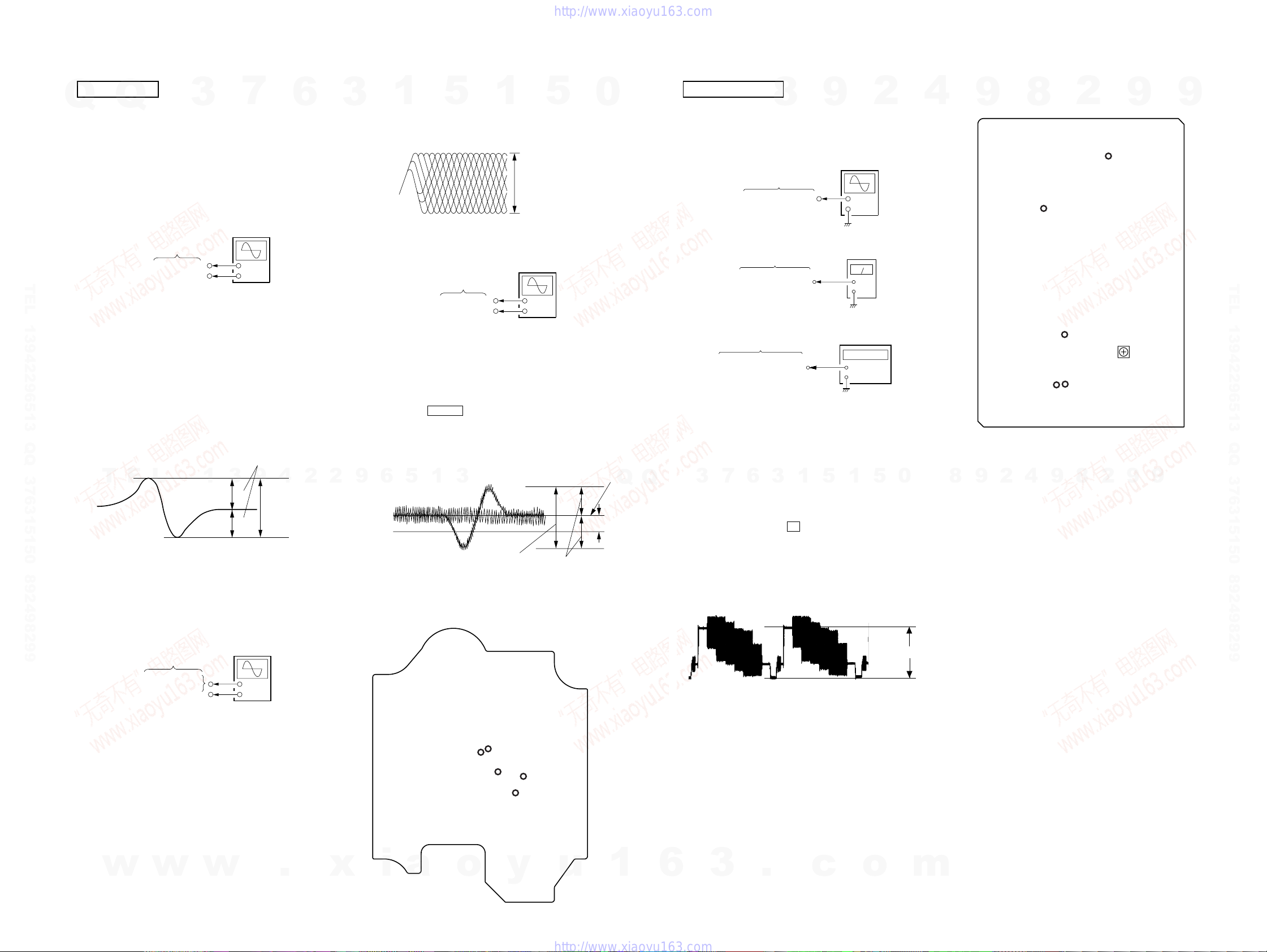
S-CURVE CHECK
TEL 13942296513 QQ 376315150 892498299
Procedure :
1. Connect an oscilloscope to TP68 (FE) and TP73 (DVC) on the
2. Turn the power ON.
3. Load a disc (LUV-P01) and actuate the focus search. (In
4. Confirm that the oscilloscope waveform (S-curve) is
Note: •Try to measure several times to make sure than the ratio
Q
check each item in order given.
signal level is low than specified value with the following checks.
TP73 (DVC)
BD board.
consequence of open and close the disc tray, actuate the focus
search)
symmetrical between A and B. And confirm peak to peak level
within 2 ± 0.5 Vp-p.
S-curve waveform
T
E
L
of A : B or B : A is more than 10 : 7.
•Take sweep time as long as possible and light up the
brightness to obtain best waveform.
3
BD board
TP68 (FE)
1
7
oscilloscope
+
–
symmetry
3
9
A
within 2
B
4
6
2
±
0.5Vp-
2
Note: Clear RF signal waveform means that the shape “ ◊ ” can be clearly
3
9
1
TRAVERSE LEVEL CHECK
Procedure :
1. Connect an oscilloscope to TP70 (TE) and TP73 (DVC) on the
BD board.
2. Turn the power ON.
3. Load a disc (LUV-P01) and playback the number nine track.
4. Press the hH button. (Becomes the 1 track jump mode.)
5. Confirm that the level B and A (DC voltage) on the oscilloscope
waveform.
1 track jump waveform
6
DVC
Connecting Location:
distinguished at the center of the waveform.
5
5
RF signal waveform
BD board
TP70 (TE)
TP73 (DVC)
1
3
level=1.2 ±0.55Vp-p
1
VOLT/DIV : 200mV
TIME/DIV : 500ns
5
level : 0.75
1.05 ±0.3Vp-p (RFAC)
oscilloscope
+
–
B
symmetry
0
±
0.1Vp-p (RFDC
center of
waveform
A (DC voltage
Q
Q
2
+
–
level meter
+
–
5
1
1
9
oscilloscope
5
VIDEO LEVEL ADJUSTMENT
(AUDIO LEVEL/VIDEO CLOCK/AUDIO SERVO
CLOCK CHECK)
Procedure :
1. Connect an oscilloscope to TP308 (V-OUT) on the VIDEO
board.
2. Connect a level meter to TP415 (L-OUT) and TP413 (R-OUT)
on the VIDEO board.
3. Connect a frequency counter to TP70 (54 MHz) and TP182
3. Turn the power ON.
4. Set a test disc (HLV-402 (Part No. 8-909-870-00))
5. Press three buttons x , [ENTER], and [OPEN/CLOSE]
6. The message “MPEG A V TEST” is displayed on the fluorescent
7. Adjust the RV501 on the VIDEO board for 0.714 ± 0.05 Vp-p.
Note: TP308 (V-OUT) on the VIDEO board must be teminated by 75 Ω.
7
3
(4.2336 MHz) on the VIDEO board.
simultaneously.
indicator tube. Color bar signal outputs and sine-wave (1 kHz
0dB) appears.
8
VIDEO board
TP308 (V-OUT)
VIDEO board
TP415 (L-OUT)
TP413 (R-OUT)
3
6
4
0
Connecting and Adjustment Location:
TP182
9
2
TP413
(R-OUT)
8
2
8
TP70
(54 MHz)
(4.2336 MHz)
TP415
(L-OUT)
4
9
– VIDEO BOARD (Component Side) –
9
8
TP308
(V-OUT)
2
9
RV501
Video
Level
Adjustment
9
9
9
TEL 13942296513 QQ 376315150 892498299
RF LEVEL CHECK
BD board
TP71 (RFDC)
TP72 (RFAC)
TP73 (DVC)
Procedure :
1. Connect an oscilloscope CH1 to TP71 (RFDC), CH2 to TP72
(RFAC) and TP73 (DVC) on the BD board.
2. Turn the power ON.
3. Load a disc (LUV-P01) and playback the number nine track.
4. Confirm that oscilloscope waveform is clear and check if RF
signal level is correct or not.
w
w
oscilloscope
w
+
–
.
x
– BD BOARD (Conductor Side) –
TP68
(FE)
TP72
(RFAC)
i
a
TP70
(TE)
o
TP73
(DVC)
y
TP71
(RFDC)
u
1
0.714 ± 0.05 Vp-p
8. Confirm that the value of level meter is 2.5 ± 2.0 dBs. (If audio
output disappear, press the [PLAY MODE] button twice)
9. Confirm that the value of frequency counter is 54 MHz ± 400
Hz.
10. Confirm that the value of frequency counter is 4,2336 MHz.
11. Change disc to a MP3 test disc (MP3 1kHz 0dB sine-wave is
recorded)
12. Confirm that the value of level meter is 2.4 ± 2.0 dBs.
6
3
2121
.
c
o
m
HCD-RV7/RV8
SECTION 7
DIAGRAMS
7-1. BLOCK DIAGRAM – CD SERVO Section –
Q
Q
3
DETECTOR
TEL 13942296513 QQ 376315150 892498299
OPTICAL PICK-UP
BLOCK
(A-MAX. 3)
LASER DIODE
LD
PD
7
6
7
8
9
11
10
AUTOMATIC
POWER
CONTROL
Q101
6
A
B
C
D
F
E
F I-V AMP
E I-V AMP
LD
1
3
SUMMING
1
FOCUS/TRACKING ERROR AMP
RF
AMP
FOCUS
ERROR AMP
RF DC
AMP
TRACKING
ERROR AMP
APC LD
AMP
AC
SUM
RFDCO
RFDCI
SW
RF AMP,
IC103
FE
FEI
TE
PD
4
16
17
28
29
18
12
2
5
1
EQ
IN
RFAC
3
VCA
5
SELECT SWITCH
26
RFC
RFAC
EQ
D/A1
D/A3
D/A4
D/A2
FREQUENCY
Q102
15
0
8
FILTER
171
168 170
RFAC
173
FE
164
RFDC
160
TE
162
SE
163
MDP
SFDR
SRDR
133
137 138 140
FILO
DIGITAL SIGNAL PROCESSOR,
DIGITAL SERVO PROCESSOR
IC505 (1/2)
TFDR
TRDR
FFDR
141
142
143
PCO
FRDR
CLTV
135
169
SSTP
FILI
XTAO
150 149
X501
33.8688MHz
9
XTSL
PCMD
BCK
LRCK
C2PO
DATA
CLOK
XLAT
SENS
SCOR
SQSO
L SQCK
L SCLK
GFS
L FOK
L CDXRST
XTAI
TBL-SENS
2
189
91
93
88
124
102
111
109
113
126
96
98
114
121
131
105
49
4
DATA
BCK
LRCK
C2PO
DATA
CLOK
XLAT
SENS
SCOR
SQSO
SQCK
SCLK
GFS
FOK
XRST
DISC TRAY
STATUS SENSOR
IC711
9
8
2
DATA, CLOK, XLAT, SENS,
SCOR, SQSO, SQCK,
SCLK, GFS, FOK, XRST
• R-ch is omitted due to same as L-ch.
• SIGNAL PATH
: CD PLAY
CONT
DATA, BCK,
LRCK, C2PO
9
A
B
C
(Page 23)
(Page 23)
(Page 23)
9
TEL 13942296513 QQ 376315150 892498299
T
E
L
(TRACKING)
(FOCUS)
ON :
1
2-AXIS
DEVICE
(LIMIT)
When the optical
pick-up is inner
position
3
9
M101
(SPINDLE)
M102
(SLED)
FOCUS/TRACKING COIL DRIVE,
4
M
M
SPINDLE/SLED MOTOR DRIVE
2
2
9
IC102
VO4+
5
VO4–
10
VO3+
1
VO3–
2
VO2+
56
VO2–
55
VO1+
47
VO1–
52
MOTOR
DRIVE
MOTOR
DRIVE
COIL
DRIVE
COIL
DRIVE
8
STBY
6
IN4
IN3+
IN3–
IN2+
IN2–
IN1+
IN1–
5
23
27
26
32
31
35
34
1
3
Q
Q
3
7
6
BU UP/DOWN-SW
1
3
CLOSE-SW 47
SYSTEM CONTROLLER
(CD MECHANISM CONTROL)
IC501 (1/4)
SYSRST
43
1
5
OPEN-SW 46
LOAD-OUT 45
LOAD-IN
SHARPNESS
HUE
48
44
D/A1
D/A2
D/A3
D/A4
5
OPEN
CLOSE
0
TURN MOTOR
FIN
7
RIN
9
3
AO3
5
AO4
AO5
6
CONVERTER
9
AO6
13
AO1
AO2
2
S711
OPTICAL PICK-UP
UP/DOWN DETECT
9
8
S701
DISC TRAY OPEN/CLOSE
DETECT
DRIVER
IC701
DRIVE
D/A
IC506
4
OUT2
OUT1
DI
CLK
LD
RST
MOTOR
9
9
2
8
9
4
2
DATA
CLK
M721
M
(TURN)
DATA, CLK, LD
LD
SYSRST
SHARPNESS, HUE
D
E
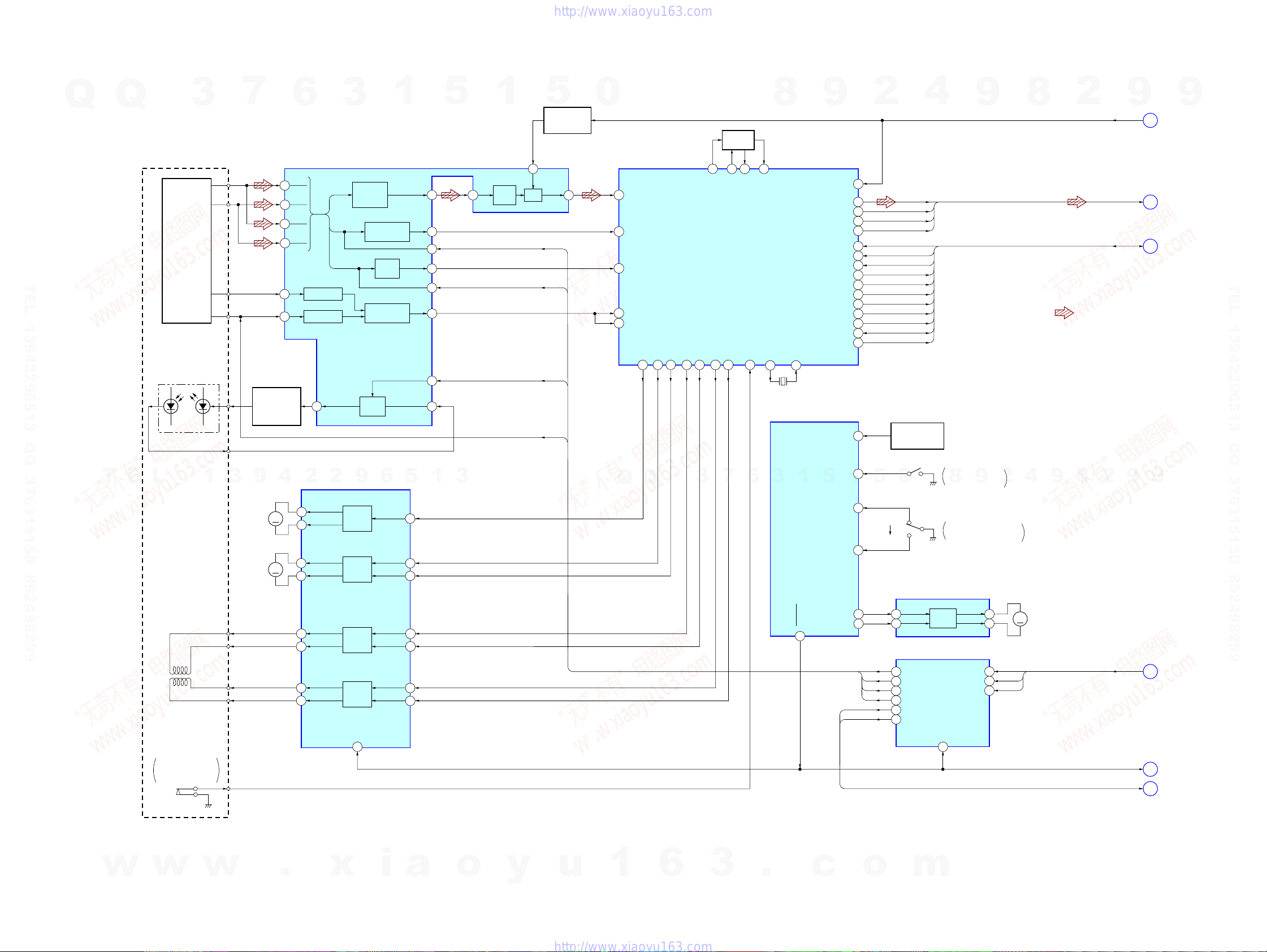
F
(Page 23)
(Page 23)
(Page 23)
2
4
12
11
10
w
w
w
.
x
i
a
o
y
u
1
6
2222
3
.
c
o
m
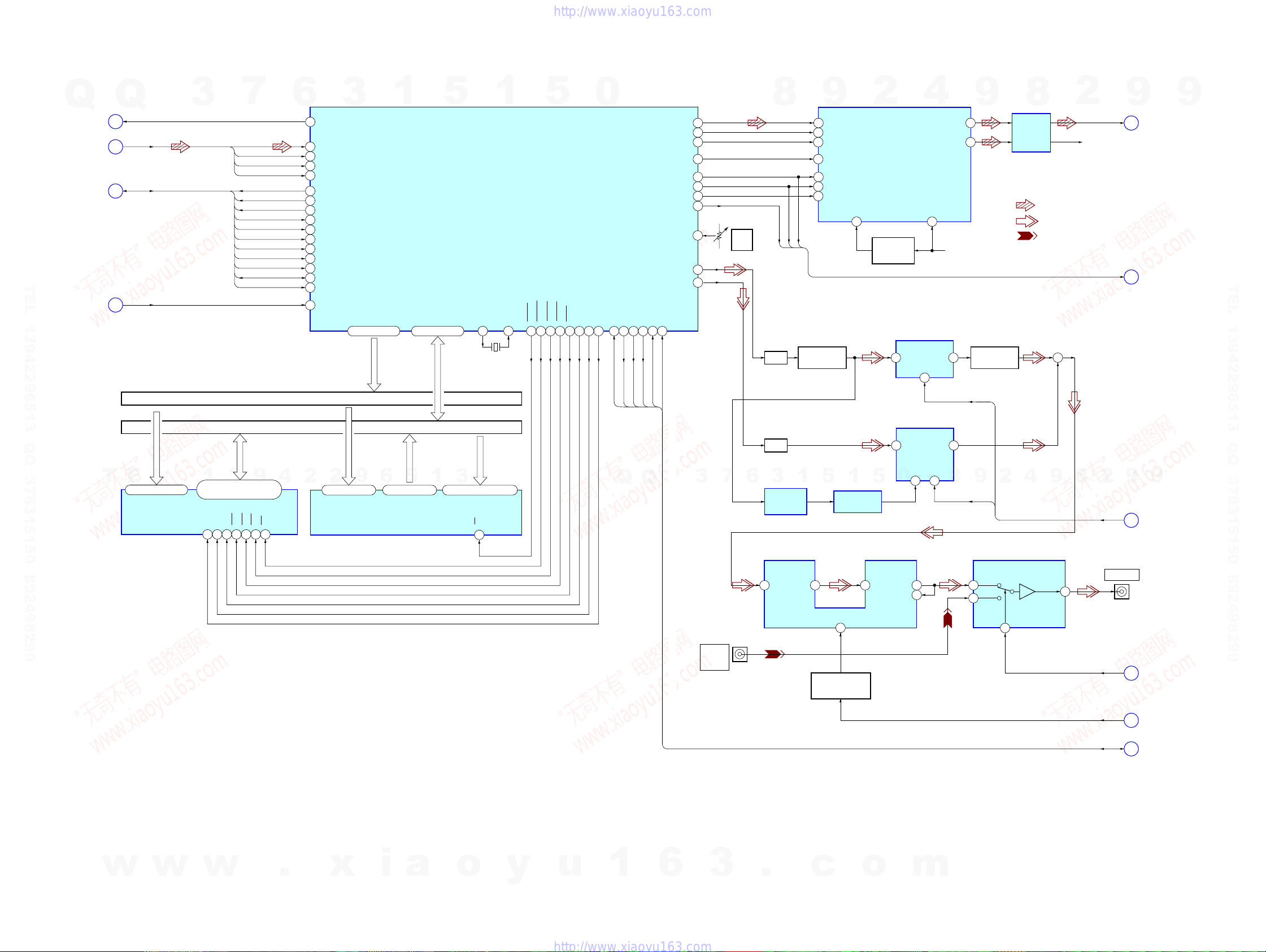
7-2. BLOCK DIAGRAM – AUDIO/VIDEO CD Section –
Q
(Page 22)
(Page 22)
(Page 22)
Q
CONT
A
DATA, BCK,
LRCK, C2PO
B
DATA, CLOK, XLAT, SENS,
SCOR, SQSO, SQCK,
SCLK, GFS, FOK, XRST
C
3
TEL 13942296513 QQ 376315150 892498299
(Page 22)
SYSRST
E
7
DATA
BCK
LRCK
C2PO
DATA
CLOK
XLAT
SENS
SCOR
SQSO
SQCK
SCLK
GFS
FOK
XRST
6
24
90
92
87
123
103
110
108
112
125
95
99
115
120
132
106
81
3
GPIO9
L CDDATA
L CDBCK
L CDLRCK
L CDC2PO
L DDAT
L DCLK
L XLAT
L SENS
L SCOR
L SQSO
SQCK
SCLK
L GFS
FOK
XRST
SYSRST
DRADR0 – DRADR10
34 – 37, 39 – 45 49 – 56, 59 – 66
1
5
DRDAT0 – DRDAT15
1
MPEG VIDEO/AUDIO DECODER,
VIDEO SIGNAL ENCODER
IC505 (2/2)
CLKB
CLKA
NVOEL
207 206
741873 72 68
5
DRRAS
DRWEL
DRCAS
DRBS
DRCK
70 76 77 78
0
DRDQM1
DRDQM0
GPIO0
13 14
GPIO1
GPIO5
GPIO2
15 19 18 16
AUDDTO0
AUDBCK
AUDLRCK
AUDXCLKO
GPIO14
GPIO13
GPIO11
GPIO12
CPSIG
CSIG
GPIO3
GPIO4
VRF
HCD-RV7/RV8
2
DIGITAL FILTER,
D/A CONVERTER
VDD
5
IC504
+3.3V
REGULATOR
Q581
CLK
DATA
9
2
1
3
16
13
14
15
DATA
BCK
LRCK
MLCK
DATA
CLK
LAT
8
201
203
204
205
30
29
26
28
RV501
3
6
7
VIDEO
LEVEL
LD
4
Y AMP
IC304
6
VCC
VOUTL
VOUTR
CD D+5V,
CD A+5V
9
7
8
8
LOW-PASS
FILER
IC102
• R-ch is omitted due to same as L-ch.
• SIGNAL PATH
2
CD L-CH
R-CH
: CD PLAY (AUDIO)
: CD PLAY (VIDEO)
: GAME INPUT (VIDEO)
DATA, CLK, LD
9
G
D
(Page 25)
(Page 22)
9
TEL 13942296513 QQ 376315150 892498299
T
A0 – A10
E
L
23 – 26, 29 – 34, 22
A0 – A10
D-RAM
IC507
D0 – D15
1
3
DQ0 – DQ15
BA0
CLK
3815
CAS
9
RAS
161720
2, 4, 5, 7, 8, 10, 11, 13, 42,
44, 45, 47, 48, 50, 51, 53
LDQM
UDQM
39
WE
4
ADDRESS BUS
DATA BUS
2
12 – 5, 27, 26, 31
PROGRAM ROM
A0 – A10
2
A0 – A9, A18
IC508
9
A0 – A10
6
D0 – D7
5
13 – 15, 17 – 21
DQ0 – DQ7
D0 – D15
1
3
23, 25, 4, 28, 29, 3, 2, 30
A10 – A17
X502
27MHz
D8 – D15
OE
24
SDO
Q
SDI
SCK
SCS
Q
SOK
SRQ
3
J601(1/2)
GAME
INPUT
VIDEO
7
6
B.P.F.
B.P.F.
3
SYNC
SEPARATOR
IC301
VIDEO AMP
IC307
BUF
8
IN
SYNC BUFFER
Q301
1
BUF
1
OUT
1
5
C SYNC BUFFER
IC302
STBY
2
VIDEO MUTING
CONTROL SWITCH
Q370
Y SYNC BUFFER
10
VIN
CONT IN
C AMP
IC303
1
VIN
BGP8TINT
0
5
3
IN
OUT
OUTSAG
5
6
5
1
VOUT
5
6
VOUT
8
SHARPNESS
9
HUE
1
3
Q302
2
VIDEO SELECT SWITCH,
VIDEO AMP
IC781
VIN1
VIN2
SW1
2
4
VOUT
9
+
7
8
SHARPNESS,
2
HUE
J401
VIDEO OUT
V SW
9
F
H
9
(Page 22)
(Page 25)
w
w
w
.
x
i
a
o
y
u
1
6
2323
3
.
c
o
m
V MUTE
SDO, SDI, SCK,
SCS, SOK, SRQ
J
K
(Page 25)
(Page 25)
HCD-RV7/RV8
7-3. BLOCK DIAGRAM – TUNER/TAPE DECK Section –
FM 75Ω
Q
AM
Q
ANTENNA
FM ANT
ANT GND
AM ANT
ANT GND
3
TUNER UNIT
L-CH
R-CH
ST-DOUT
ST-DIN
ST-CLK
ST-CE
ST-MUTE
TUNED
STEREO
7
6
R-CH
DI
DO
CLK
CE
MUTING
TUNED
STEREO
3
1
5
1
DECK A/B SELECT SWITCH,
PB EQ AMP
IC301 (1/2)
5
0
8
9
2
4
9
8
2
9
TUNER
L-CH
L
9
(Page 25)
TEL 13942296513 QQ 376315150 892498299
L-CH
HP901
(PB)
R-CH
L-CH
R-CH
HRPE901
(REC/PB/ERASE)
RV354
REC BIAS (R)
(DECK B)
T
M901
(CAPSTAN)
E
R-CH
R-CH
R-CH
L
MM
RV1002
TAPE SPEED
(NORMAL)
1
RV304
REC BIAS (L)
(DECK B)
BIAS OSC
T301
BIAS OSC
Q302, 303
CAPSTAN
MOTOR DRIVE
Q396, 397
CAPSTAN MOTOR
CONTROL SWITCH
Q1001
R-CH R-CH
2
3
BIAS
TRAP
Q301, 307, 310
RV1001
TAPE SPEED
13
9
REC BIAS
SWITCH
Q395
(HIGH)
REC/PB SWITCHING
IC302
4
2
TC +10V
4
REC/PB
SWITCHING
Q304, 305
2
9
65 BIAS
55 CAPM-CNT1
54 CAPM-H/L
D +3.3V
6
69
TC-RELAY
A-PLAY
56
S1001
(DECK A PLAY)
5
DI
DO
25
23
27
ST-DIN
ST-DOUT
(DECK B PLAY)
CLK
ST-CLK
S1002
1
CE
22
57
MUTING
21
ST-CE
ST-MUTE
B-PLAY
3
TUNED
STEREO
3
2
TUNED
32
34
STEREO
AIN1
BIN1
REC EQ AMP, ALC
RECOUT1
21
ALC ON/OFF
11
68
ALC
S1003
(DECK A HALF)
REC MUTE ON/OFF
15 13 12 14
A/B
REC MUTE
IC301 (2/2)
EQ
R-CH
A-HALF
70
D +3.3V
EQOUT1
A/B
NORMAL/HIGH SPEED
MUTE ON/OFF
NOR/HIGH
ALC
R-CH
S1006
(DECK B HALF)
S1009
(DECK B REC)
28 27
+
R-CH
Q
Q
REC-IN1
24
ALC1
23
B-HALF
91
D +3.3V
S1005
(DECK A REC)
TAI1
3
RV301
REC LEVEL (L)
(DECK B)
ROTATION
DETECT SENSOR
(DECK A)
IC1001
MUTE
SYSTEM CONTROLLER
(CD MECHANISM CONTROL)
A-SHUT
89
7
PB-OUT1
6
A/B
NOR/HIGH
REC MUTE
PB-A/B
REC-MUTE
IC501 (2/4)
3
EQ-H/N
ROTATION
DETECT SENSOR
(DECK B)
IC1002
26
MUTING
Q306
MUTING CONTROL
SWITCH
Q389
1
58 5361 67 66
TC-MUTE
B-SHUT
90
LOW-PASS
FILTER
IC303
1
5
PM901
TRIGGER PLUNGER
(DECK A)
Q390, 398, 399
0
5
A-TRIG
51
TRIGGER
PLUNGER DRIVE
(DECK A)
Q393, 394
BUFFER
9
8
AMS-IN
B-TRIG
52
TRIGGER
PLUNGER DRIVE
(DECK B)
Q391, 392
4
2
PM902
TRIGGER PLUNGER
(DECK B)
TAPE
L-CH
• R-ch is omitted due to same as L-ch.
• SIGNAL PATH
: TUNER (FM/AM)
: TAPE PLAY (DECK A)
: TAPE PLAY (DECK B)
: REC
9
2
8
9
L-CH
REC
M
N
(Page 25)
9
(Page 25)
TEL 13942296513 QQ 376315150 892498299
w
w
w
.
x
i
a
o
y
u
1
6
2424
3
.
c
o
m
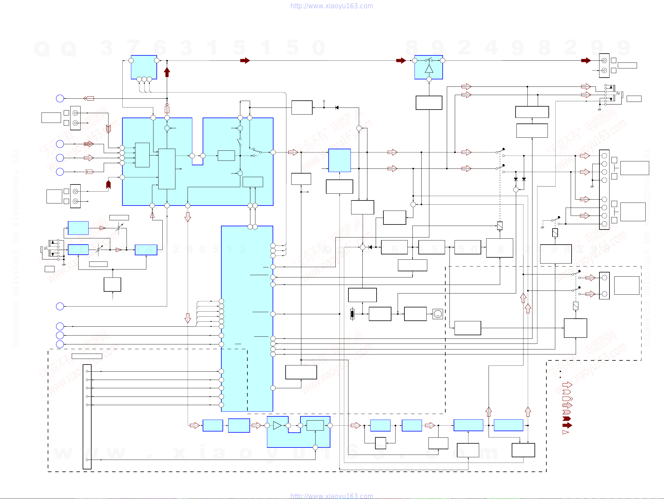
7-4. BLOCK DIAGRAM – MAIN Section –
HCD-RV7/RV8
SURROUND SIGNAL
PROCESSOR
IC181
6
4
5
3
7
RV721
ECHO LEVEL
3
MIC
Q721
7
10
L-OUT
IND1
INB1
INC1
INA1
INEX1
9
BP/SR
2
1
SUR2
SUR1
INPUT
SELECT
SWITCH
MIC AMP
IC722 (2/2)
6
L-IN
CONT23CONT3
SUR3
42
SUR1
MIC
2
4
.
7
RECB1
SOUND
CONTROL
CIRCUIT
2
8
+
SAOUT
19
3
R-CH
TOUT1
2
x
R-CH
SWOUT
24
9
CN101
1
7
5
4
6
2
3
R-CH
R-CH
1
RV722
MIC LEVEL
CONTROL
A +10V
w
Q
(Page 24)
TEL 13942296513 QQ 376315150 892498299
(Page 23)
(Page 24)
(Page 24)
(Page 26)
(Page 23)
(Page 23)
(Page 23)
Q
N
MD/VIDEO
(AUDIO) IN
G
L
M
GAME
INPUT
AUDIO
T
J721
MIC
P
K
J
H
SW-SOLID-LED
SW-LINK-LED
SW-MTRX-SURR-LED
SW-WIDE-LED
w
(RV8)
REC L-CH
J750
L
R
CD L-CH
TUNER L-CH
TAPE L-CH
J601 (2/2)
L
R
DIGITAL
ECHO
IC721
MIC AMP
E
L
IC722 (1/2)
SPEANA
SDO, SDI, SCK,
SCS, SOK, SRQ
V MUTE
V SW
SYSTEM CONTROL
(TO SS-WGV8)
AD-KEY
w
VOLUME
1
INPUT SELECT SWITCH,
ELECTRICAL VOLUME
VOLIN1
15
14
6
SDO
SDI
SCK
SCS
SOK
SRQ
IC901 (2/2)
i
TONE CONTROL,
BUFFER
5
IC102
R-CH
VOLUME
CONTROL
R-CH
5
1
SYSTEM CONTROLLER
(CD MECHANISM CONTROL)
35
SYSOUT
36
SYSIN
37
SYSCLK
19
SYSCS
32
SYSOK
40
SYSRQ
33 VIDEO MUTE
VIDEO-OUT
76
GAME/VCD
94 SW-AD-KEY
59 SW-ON-LED
71 SW-LINK-LED
SW-MATRIX-
72
SURR-1-LED
SW-MATRIX-
60
SURR-2-LED
LOW-PASS
IC901 (1/2)
a
+
+
3
IC501 (3/4)
FILTER
o
1716
BB B1
BB A1
CPU
INTERFACE
DATA
CLOCK
2221
81 82
GEQ DATA
AUDIO-OUT
1
OUT1
GEQ CLK
ON/OFF
2
ELECTRICAL VOLUME
y
18
SUR1
5SUR1
SUR2
6SUR2
SUR3
7SUR3
77
88PROTECTOR
87FRONT-RELAY
83STK-MUTE
78HP MUTE
79HP-DETECT
86LINK-RELAY
97SW RELAY
80LINE-MUTE
5
MUTING CONTROL
4
LINE AMP,
IC902
FEED BACK
SWITCH
Q101
MUTING
Q103
SWITCH
Q504, 505
7
u
0
R-CH
R-CH
VOLUME
CONTROL
8
R-CH
Q
1
D841
POWER AMP
IC501
STANDBY
SWITCH
Q503, 504, 581
Q
9
6
+
OVER LOAD
DETECT
Q501, 551
+
TEMPERATURE
DETECT SWITCH
Q505, 506
TH701
D502
3
DETECT SWITCH
7
FAN MOTOR
ON SWITCH
Q831
LINE AMP
IC903 (1/2)
AGC
Q905
3
DC DETECT
SWITCH
Q507, 508
OVER LOAD
Q509
6
.
AUDO OUT
ON/OFF SWITCH
8
3
AUDIO OUT
ON/OFF SWITCH
+
DETECT SWITCH
1
3
PROTECT SWITCH
Q502
FAN MOTOR
DRIVE
Q891, 892
FILTER AMP
IC903 (2/2)
IC430
9
5
Q430
OVER LOAD
Q510
5
M891
(FAN)
MUTING
Q999
c
R-CH
9
J430
T501
–
+
–
9
L
AUDIO OUT
R
J631
PHONES
TEL 13942296513 QQ 376315150 892498299
+
L
FRONT SPEAKER
IMPEDANCE
USE 6–16Ω
R
2
4
4
–2
–1
9
HEADPHONE MUTING
Q812, 862
MUTING CONTROL
SWITCH
Q861
D507
D511
8
2
+
+
L
–
+
1
OVER LOAD
DETECT SWITCH
Q511
0
5
RY501
FRONT SPEAKER
PROTECT
RELAY DRIVE
8
Q512
9
2
SURROUND
9
4
SPEAKER PROTECT
RELAY DRIVE
Q513
RY502
8
2
–1
9
–
9
TM801
+
–2
–
RY801
M
OVER LOAD
DETECT SWITCH
Q825
SUB WOOFER AMP
IC502 (1/2)
STANDBY
SWITCH
Q1001-1003
o
m
SUB WOOFER AMP
IC502 (2/2)
OVER LOAD
Q1004, 1054
DETECT
SUB WOOFER
PROTECT
RELAY DRIVE
Q824
R-ch is omitted due to same as L-ch.
SIGNAL PATH
: TUNER (FM/AM)
: TAPE PLAY
: REC
: CD PLAY
: MD/VIDEO (AUDIO) IN
: GAME INPUT (AUDIO)
: AUDIO OUT
: MIC INPUT
SURROUND
IMPEDANCE
R
SUB WOOFER
OUT
IMPEDANCE
USE 8Ω
SPEAKER
USE 24Ω
2525
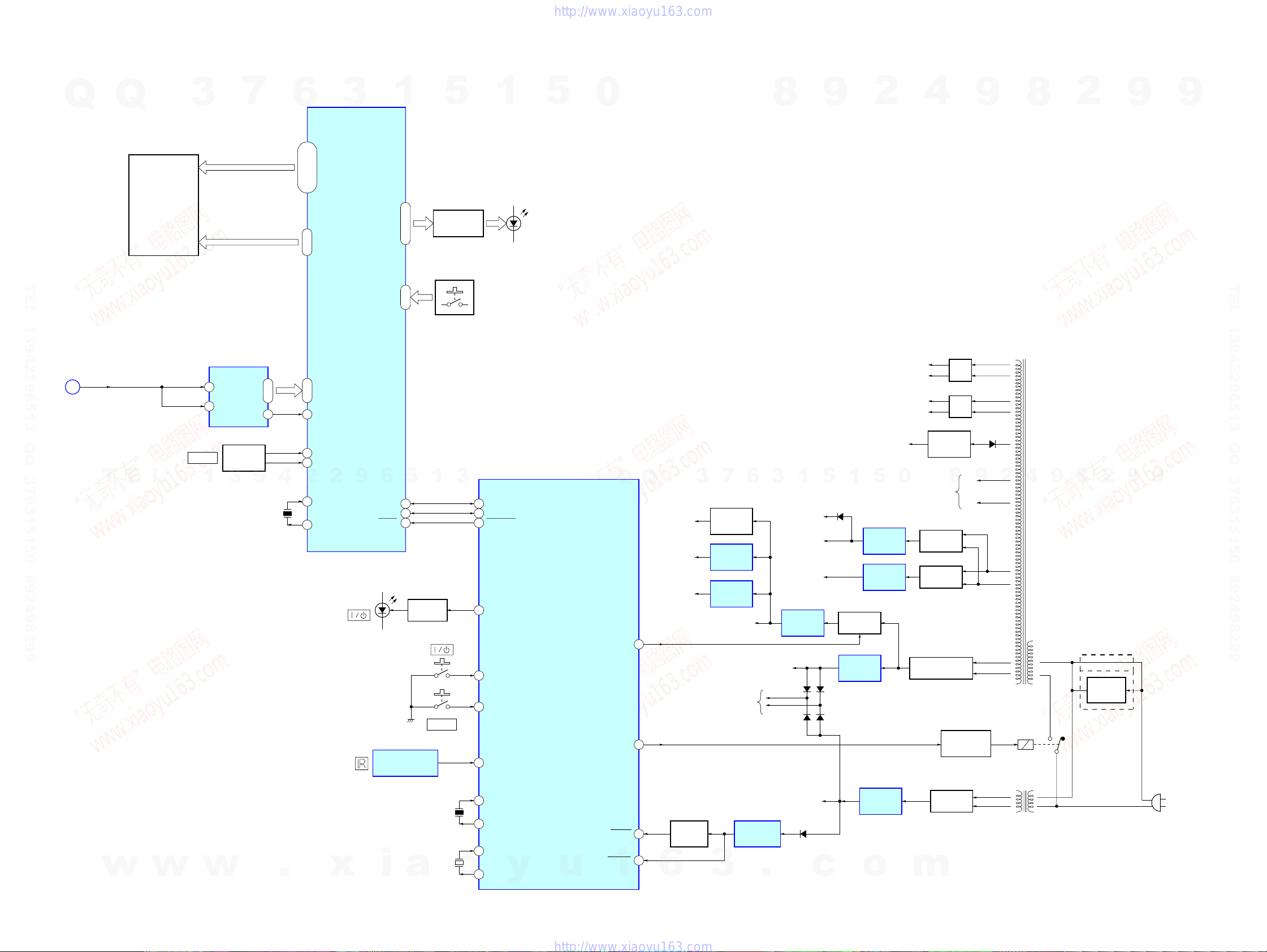
HCD-RV7/RV8
7-5. BLOCK DIAGRAM – DISPLAY/KEY CONTROL/POWER SUPPLY Section –
Q
Q
FL601
FLUORESCENT
INDICATOR TUBE
3
7
6
1 – 10, 12 – 22,
100 – 86
3
P1 – P41
24 – 41, 43, 44
1G – 15G
LED-MD-VIDEO,
LED-TAPE,
LED-TUNER,
LED-CD,
LED-GAME,
LED-DISC1,
LED-DISC2,
LED-DISC3,
LED-REC
1
52 – 59, 74
5
LED DRIVE
Q601 – 605,
Q791 – 793, 795
1
5
D604 – 608,
D791 – 793, 795
0
8
9
2
4
9
8
2
9
9
TEL 13942296513 QQ 376315150 892498299
KEY0 – KEY2
FLUORESCENT
INDICATOR TUBE DRIVER,
KEY CONTROL
67 – 72
BPF0 – BPF5
73 ALL-BAND
80 VOLUME-A
79 VOLUME-B
2
2
83 X1
82 X0
x
IC601
9
D794
6
REMOTE CONTROL
RECEIVER
IC603
i
(Page 25)
X
P
SPEANA
T
E
w
L
w
VOLUME
1
w
BAND-PASS
FILTER
4 LINE IN
6REC IN
3
IC602
ROTARY
ENCODER
S748
F01 – F06
11L+R
9
X601
4MHz
17 – 12
4
.
64 – 66
5
60I2C-DATA
61I2C-CLOCK
77RESET
LED DRIVE
a
1
Q794
S749
S750
DISPLAY
X502
16MHz
X501
32.768kHz
3
30 IIC-DATA
29 IIC-CLK
41 GC-RESET
75 STBY-LED
74 POWER-KEY
73 DISPLAY-KEY
15 X-IN
13 X-OUT
10 XC-IN
o
11 XC-OUT
S751 – 792
4SIRCS
SYSTEM CONTROLLER
(CD MECHANISM CONTROL)
IC501 (4/4)
y
u
Q
1
38SYSPWR
84STBY-RELAY
12RESET
20AC-CUT
Q
D D +3.3V
6
+4.5V
+2.5V
RESET
SWITCH
Q601
3
7
+4.5V
REGULATOR
Q201
+2.5V
REGULATOR
IC201
+3.3V
REGULATOR
IC202
CD D+5V
CD A+5V
3
6
D +3.3V
RESET SIGNAL
GENERATOR
IC601
3
D +4V
.
5
1
D920 – 922
M +7V
M +9V
A +10V
TC +10V
+5V
REGULATOR
IC911
D501 D503
D502 D504
EVER +4V
D505
c
1
REGULATOR
REGULATOR
B+ SWITCH
Q911, 912
+4V
REGULATOR
IC951
REGULATOR
o
5
+9V
IC961
+10V
IC101
+4V
IC971
+VL
–VL
+VH
–VH
– VG
0
TO FLUORESCENT
INDICATOR TUBE
FL601
D918, 919, 923, 924
m
– 33V
REGULATOR
Q941
RECT
D914 – 917
RECT
D906 – 909
RECT
POWER ON/OFF
RELAY DRIVE
RECT
D972 – 975
RECT
RECT
8
D541
D543
Q971
VF1
VF2
9
TRANSFORMER
RECT
D977
2
T910
MAIN POWER
4
RY971
T972
SUB POWER
TRANSFORMER
9
2
8
(RV7: Thai)
VOLTAGE
SELECTOR
S901
(EXCEPT RV7: Thai)
9
TEL 13942296513 QQ 376315150 892498299
9
(AC IN)
2626
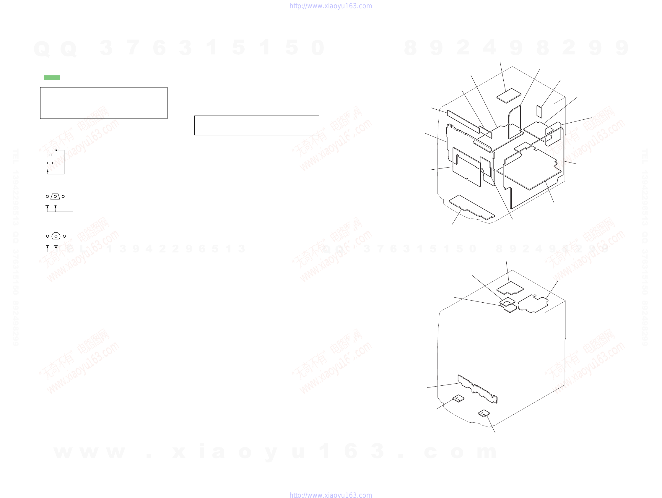
MOTOR board
SENSOR (CD) board
DRIVER board
BD board
SW board
HEAD (A) board
HEAD (B) board
MAIN TRANS board
SENSOR board
SUB WOOFER board
(HCD-RV8)
TUNER PACK
MAIN board
POWER board
PANEL board
CD SWITCH board
CD OPEN board
PAD SWITCH board
GAME IN board
VOL board
VIDEO board
SUB-TRANS board
HCD-RV7/RV8
7-6. NOTE FOR PRINTED WIRING BOARDS AND SCHEMATIC DIAGRAMS
Q
Note on Printed Wiring Board:
• X : parts extracted from the component side.
• Y : parts extracted from the conductor side.
• : Pattern from the side which enables seeing.
(The other layers' patterns are not indicated.)
• VIDEO board is multi-layer printed board.
• Indication of transistor.
TEL 13942296513 QQ 376315150 892498299
Q
Caution:
Pattern face side: Parts on the pattern face side seen from
(Conductor Side) the pattern face are indicated.
Parts face side: Parts on the par ts face side seen from
(Component Side) the parts face are indicated.
However, the patterns of intermediate-layer have not been
included in diagram.
C
Q
B
B
B
These are omitted.
E
Q
CE
These are omitted.
Q
CE
T
E
These are omitted.
L
3
1
7
3
9
6
4
2
2
3
1
Note on Schematic Diagram:
• All capacitors are in µF unless otherwise noted. pF: µµF
50 WV or less are not indicated except for electrolytics
and tantalums.
• All resistors are in Ω and 1/
specified.
f
•
• 2 : nonflammable resistor.
• 5 : fusible resistor.
• C : panel designation.
Note: The components identified by mark 0 or dotted line
with mark 0 are critical for safety.
Replace only with part number specified.
• A : B+ Line.
• B : B– Line.
• H : adjustment for repair.
•Voltages are taken with a V OM (Input impedance 10 MΩ).
Voltage variations may be noted due to normal production tolerances.
•Waveforms are taken with a oscilloscope.
Voltage variations may be noted due to normal production tolerances.
• Circled numbers refer to waveforms.
• Signal path.
F : TUNER (FM/AM)
E : TAPE PLAY (DECK A)
d : TAPE PLAY (DECK B)
G : REC
J : CD PLAY (AUDIO)
L : CD PLAY (VIDEO)
q : MD/VIDEO (AUDIO) IN
j : GAME INPUT (AUDIO)
k : GAME INPUT (VIDEO)
9
6
5
f : AUDIO OUT
N : MIC INPUT
•Abbreviation
EA : Saudi Arabia model
MY : Malaysia model
SP : Singapore model
TH : Thai model
5
: internal component.
1
3
1
4
W or less unless otherwise
5
0
Q
Q
• Circuit Boards Location
8
1
3
6
7
3
9
5
1
2
5
0
4
8
9
9
2
8
4
9
2
8
2
9
9
9
TEL 13942296513 QQ 376315150 892498299
9
w
w
w
.
x
i
a
o
y
u
1
6
2727
3
.
c
o
m
 Loading...