

SONY HCD-RV2, HCD-RV5, HCD-RV6 Service Manual

HCD-RV2/RV5/RV6
SERVICE MANUAL
Ver 1.0 2002. 07
• HCD-RV2/RV5/RV6 is the tuner,
deck, CD and amplifier section in
MHC-RV2/RV5/RV6.
CD CD Mechanism Type CDM58E-30BD62
Section Base Unit Name BU-30BD62
Tape Deck
Section T ape Transport Mechanism Type
E Model
HCD-RV2/RV5/RV6
Tourist Model
HCD-RV5
Model Name Using Similar Mechanism NEW
Optical Pick-up Name A-MAX.3
Model Name Using Similar Machanism NEW
RV2: CWM43FF-05
RV5/RV6: CWM48RR-01
Amplifier section
HCD-RV2:
The following measured at AC 120, 127, 220, 240 V,
50/60 Hz
DIN power output (rated)
50 + 50 watts
Continuous RMS power output (reference)
60 + 60 watts (6 ohms at
1 kHz, 10% THD)
HCD-RV6:
The following measured at AC 120, 127, 220, 240 V,
50/60 Hz
DIN power output (rated)
115 + 115 watts
Continuous RMS power output (reference)
140 + 140 watts (6 ohms at
1 kHz, 10% THD)
HCD-RV5:
The following measured at AC 120, 127, 220, 240 V,
50/60 Hz
DIN power output (rated)
100 + 100 watts
Continuous RMS power output (reference)
120 + 120 watts (6 ohms at
1 kHz, 10% THD)
SPECIFICATIONS
Inputs
HCD-RV2:
GAME INPUT (VIDEO) (phono jack):
1 Vp-p, 75 ohms
GAME INPUT (AUDIO) (phono jacks):
voltage 450 mV,
impedance 47 kilohms
MIC (phone jack): sensitivity 1 mV,
impedance 10 kilohms
Outputs
VIDEO OUT (phono jack):
max. output level
1 Vp-p, unbalanced, Sync
negative, load impedance
75 ohms
PHONES (stereo mini jack):
accepts headphones of
8 ohms or more
SPEAKER: accepts impedance of 6 to
16 ohms
– Continued on next page –
COMPACT DISC DECK RECEIVER
9-874-131-01
2002G0400-1
© 2002. 07
Sony Corporation
Home Audio Company
Published by Sony Engineering Corporation
1

HCD-RV2/RV5/RV6
HCD-RV5/RV6:
MD/VIDEO (AUDIO) IN (phono jacks):
voltage 450/250 mV,
impedance 47 kilohms
GAME INPUT (VIDEO) (phono jack):
1 Vp-p, 75 ohms
GAME INPUT (AUDIO) (phono jack):
voltage 450 mV,
impedance 47 kilohms
MIC (phone jack): sensitivity 1 mV,
impedance 10 kilohms
Outputs
PHONES (stereo mini jack):
accepts headphones of
8 ohms or more
SPEAKER: accepts impedance of 6 to
16 ohms
SURROUND SPEAKER (HCD-RV6 only)
accepts impedance of 24
ohms
MD/VIDEO (AUDIO) OUT (phono jacks):
impedance 1 kilohms
VIDEO OUT (phono jack):
1 Vp-p,
impedance 75 ohms
Disc player section
System Compact disc and digital
audio and video system
Laser Semiconductor laser
(λ=780 nm)
Emission duration:
continuous
Frequency response 2 Hz – 20 kHz (±0.5 dB)
Wavelength 780 – 790 nm
Signal-to-noise ratio More than 90 dB
Dynamic range More than 90 dB
Video color system format
NTSC, PAL
Tape deck section
Recording system 4-track 2-channel stereo
Frequency response 40 – 13,000 Hz (±3 dB),
using Sony TYPE I
cassette
Wow and flutter ±0.15% W.Peak (IEC)
0.1% W.RMS (NAB)
±0.2% W.Peak (DIN)
Tuner section
FM stereo, FM/AM superheterodyne tuner
FM tuner section
Tuning range 87.5 – 108.0 MHz
Antenna FM lead antenna
Antenna terminals 75 ohm unbalanced
Intermediate frequency 10.7 MHz
AM tuner section
Tuning range
Middle Eastern and Philippine models:
531 – 1,602 kHz (with the
interval set at 9 kHz)
Other models: 531 – 1,602 kHz (with the
interval set at 9 kHz)
530 – 1,710 kHz (with the
interval set at 10 kHz)
Antenna AM loop antenna
Antenna terminals External antenna terminal
Intermediate frequency 450 kHz
Front speaker SS-RV900 for HCD-RV6/RV5:
Speaker system 3-way, 3-unit, bass-reflex
type
Speaker units
Sub Woofer: 13 cm, cone type
Woofer: 13 cm, cone type
Tweeter: 5 cm, cone type
Nominal impedance 6 ohms
Dimensions (w/h/d) Approx. 215 × 356 × 285 mm
Mass Approx. 4.5 kg net per
speaker
Surround speaker SS-RSV6 for HCD-RV6:
Speaker system 2-way, 2-unit, bass-reflex
type
Speaker units
Woofer: 10 cm, cone type
Tweeter: 5 cm, cone type
Nominal impedance 24 ohms
Dimensions (w/h/d) Approx. 150 × 325 × 220 mm
Mass Approx. 2.3 kg net per
speaker
General
Power requirements
Saudi Arabian model: 120 – 127 V, 220 V or
230 – 240 V AC,
50/60 Hz
Adjustable with voltage
selector
Thai model: 220 V AC, 50/60 Hz
Other models: 120 V, 220 V or 230 –
240 V AC, 50/60 Hz
Adjustable with voltage
selector
Power consumption
HCD-RV2: 115 watts
HCD-RV5: 200 watts
HCD-RV6: 220 watts
Dimensions (w/h/d)
HCD-RV2: Approx. 280 × 325 × 412 mm
HCD-RV5/RV6: Approx. 280 × 325 × 421 mm
Mass
HCD-RV2: Approx. 9.0 kg
HCD-RV5: Approx. 10.0 kg
HCD-RV6: Approx. 10.5 kg
Supplied accessories: AM loop antenna (1)
Remote Commander (1)
Batteries (2)
FM lead antenna (1)
Speaker pads (8)
Video cable (1)
Design and specifications are subject to change without
notice.
Speaker
HCD-RV2:
Speaker system 3-way, 3-unit,
bass-reflex type
Speaker units
Woofer: 13 cm, cone type
Tweeter: 5 cm, cone type
Super Tweeter: 2 cm, dome type
Nominal impedance 6 ohms
Dimensions (w/h/d) Approx. 200 × 325 × 237 mm
Mass Approx. 3.6 kg net per
speaker
2
SAFETY-RELATED COMPONENT WARNING!!
COMPONENTS IDENTIFIED BY MARK 0 OR DOTTED LINE
WITH MARK 0 ON THE SCHEMATIC DIAGRAMS AND IN
THE PARTS LIST ARE CRITICAL TO SAFE OPERATION.
REPLACE THESE COMPONENTS WITH SONY P ARTS WHOSE
PART NUMBERS APPEAR AS SHOWN IN THIS MANUAL OR
IN SUPPLEMENTS PUBLISHED BY SONY.

HCD-RV2/RV5/RV6
CAUTION
Use of controls or adjustments or performance of procedures
other than those specified herein may result in hazardous
radiation exposure.
Notes on Chip Component Replacement
• Never reuse a disconnected chip component.
• Notice that the minus side of a tantalum capacitor may be
damaged by heat.
Flexible Circuit Board Repairing
• Keep the temperature of soldering iron around 270°C during
repairing.
• Do not touch the soldering iron on the same conductor of the
circuit board (within 3 times).
• Be careful not to apply force on the conductor when soldering
or unsoldering.
NOTES ON HANDLING THE OPTICAL PICK-UP BLOCK
OR BASE UNIT
The laser diode in the optical pick-up block may suffer electrostatic
breakdown because of the potential difference generated by the
charged electrostatic load, etc. on clothing and the human body.
During repair, pay attention to electrostatic break-down and also
use the procedure in the printed matter which is included in the
repair parts.
The flexible board is easily damaged and should be handled with
care.
NOTES ON LASER DIODE EMISSION CHECK
The laser beam on this model is concentrated so as to be focused on
the disc reflective surface by the objective lens in the optical pickup block. Therefore, when checking the laser diode emission,
observe from more than 30 cm away from the objective lens.
MODEL IDENTIFICATION
– BACK PANEL –
PARTS No.
MODEL PARTS No.
RV2: E3, EA, MY, SP 4-238-649-6s
RV2: TH 4-238-649-7s
RV5: E3, EA, MY, JE, SP 4-238-649-8s
RV5: TH 4-238-649-9s
RV6: E3, EA, MY, SP 4-239-344-0s
RV6: TH 4-239-344-1s
• Abbreviation
E3 : 240 V AC area in E model
EA : Saudi Arabia model
MY : Malaysia model
SP : Singapore model
TH : Thai model
JE : T ourist model
Laser component in this product is capable
of emitting radiation exceeding the limit for
Class 1.
SETTING AND RELEASING THE CD DISC TRAY LOCK
FUNCTION
This set has a disc tray lock function to prevent discs for
demonstration at shops from theft. While this lock function is set,
the tray will not be delivered out even when the OPEN/CLOSE
button is pressed.
Setting method:
Press the OPEN/CLOSE button while pressing the STOP button.
After a few seconds, the message “LOCKED” will appear on the
fluorescent indicator tube with the tray locked.
Releasing method:
Just as the lock is set, press the OPEN/CLOSE button while
pressing the STOP button.
After a few seconds, the message “UNLOCKED” will appear with
the lock released.
3

HCD-RV2/RV5/RV6
TABLE OF CONTENTS
1. SERVICE NOTE ................................................................ 5
2. GENERAL
Main Unit (HCD-RV2) ............................................................6
Remote Control (HCD-RV2)...................................................6
Main Unit (HCD-RV5/RV6) ................................................... 7
Remote Control (HCD-RV5/RV6) .......................................... 7
3. DISASSEMBLY
3-1. Case (Top) ........................................................................... 9
3-2. Video Board......................................................................... 9
3-3. CD (Door) ......................................................................... 10
3-4. Front Panel Section ........................................................... 11
3-5. Tape Mechanism Deck ...................................................... 12
3-6. Panel Board ....................................................................... 12
3-7. Key Board ......................................................................... 13
3-8. Sensor Board, DC Fan (FAN961) ..................................... 13
3-9. Main Board, Power Amp Board ........................................14
3-10. Base Unit ...........................................................................14
3-11. Driver Board, Motor Board, Sensor (CD) Board .............. 15
4. DIAGRAMS
4-1. Circuit Boards Location .................................................... 16
4-2. Printed Wiring Board –BD Section– ................................. 18
4-3. Schematic Diagram –BD Section–.................................... 19
4-4. Printed Wiring Boards –CD Section– ............................... 20
4-5. Schematic Diagram –CD Section–.................................... 21
4-6. Printed Wiring Board –Video Section–............................. 22
4-7. Schematic Diagram –Video Section (1/2)–....................... 24
4-8. Schematic Diagram –Video Section (2/2)–....................... 25
4-9. Schematic Diagram –Main Section (1/4)– ........................ 26
4-10. Schematic Diagram –Main Section (2/4)– ........................ 27
4-11. Schematic Diagram –Main Section (3/4)– ........................ 28
4-12. Schematic Diagram –Main Section (4/4)– ........................ 29
4-13. Printed Wiring Boards –Main Section– ............................ 30
4-14. Printed Wiring Boards –Panel Section (HCD-RV2)– ....... 31
4-15. Printed Wiring Board –Key Section (HCD-RV2)– ........... 32
4-16. Schematic Diagram –Panel Section (HCD-RV2)–............ 33
4-17. Printed Wiring Boards –Panel Section (HCD-RV5)– ....... 34
4-18. Printed Wiring Board –Key Section (HCD-RV5)– ........... 35
4-19. Schematic Diagram –Panel Section (HCD-RV5)–............ 36
4-20. Printed Wiring Boards –Panel Section (HCD-RV6)– ....... 37
4-21. Printed Wiring Board –Key Section (HCD-RV6)– ........... 38
4-22. Schematic Diagram –Panel Section (HCD-RV6)–............ 39
4-23. Printed Wiring Board
–Power Amp Section (HCD-RV2)– .................................. 40
4-24. Printed Wiring Board –Trans Section (HCD-RV2)–......... 41
4-25. Printed Wiring Board
–Sub Trans Section (HCD-RV2)– ..................................... 42
4-26. Schematic Diagram –Power Section (HCD-RV2)– .......... 43
4-27. Printed Wiring Boards
–Power Amp Section (HCD-RV5)– .................................. 44
4-28. Printed Wiring Board –Trans Section (HCD-RV5)–......... 45
4-29. Printed Wiring Board
–Sub Trans Section (HCD-RV5)– ..................................... 46
4-30. Schematic Diagram –Power Section (HCD-RV5)– .......... 47
4-31. Printed Wiring Boards
–Power Amp Section (HCD-RV6)– .................................. 48
4-32. Printed Wiring Board –Trans Section (HCD-RV6)–......... 49
4-33. Printed Wiring Board
–Sub Trans Section (HCD-RV6)– ..................................... 50
4-34. Schematic Diagram –Power Section (HCD-RV6)– .......... 51
4-35. IC Block Diagrams............................................................ 52
5. EXPLODED VIEWS
5-1. Main Section ..................................................................... 56
5-2. Front Panel Section ........................................................... 57
5-3. Main Board Section .......................................................... 58
5-4. CD Mechanism Deck Section ........................................... 59
5-5. Optical Pick-up Section..................................................... 60
6. ELECTRICAL PARTS LIST ........................................ 61
4

SECTION 1
d
SERVICE NOTE
REMOVING THE PANEL BOARD AND THE KEY BOARD
* The panel board and the key board only are connected to the front panel
by means of hot-melting the plastics.
2
PANEL board
HCD-RV2/RV5/RV6
4
KEY boar
1
Cut the fifteen melted-connection points
with a cutting plier.
Note for installing the panel board and the key board
PANEL board
(eleven screw holes)
3
Cut the seven melted-connection points
with a cutting plier.
KEY board
(six screw holes)
Screw hole
In order to re-install the panel board and the key board,
fix them by using the screws (+BVTP 2.6
Screw in to the respective screw holes.
Do not tighten the screws excessively.
×
8 ) respectively.
Hot melt
5

HCD-RV2/RV5/RV6
SECTION 2
GENERAL
This section is extracted
from instruction manual.
(HCD-RV2)
(HCD-RV2)
6

HCD-RV2/RV5/RV6
(HCD-RV5/RV6)
(HCD-RV5/RV6)
7
HCD-RV2/RV5/RV6
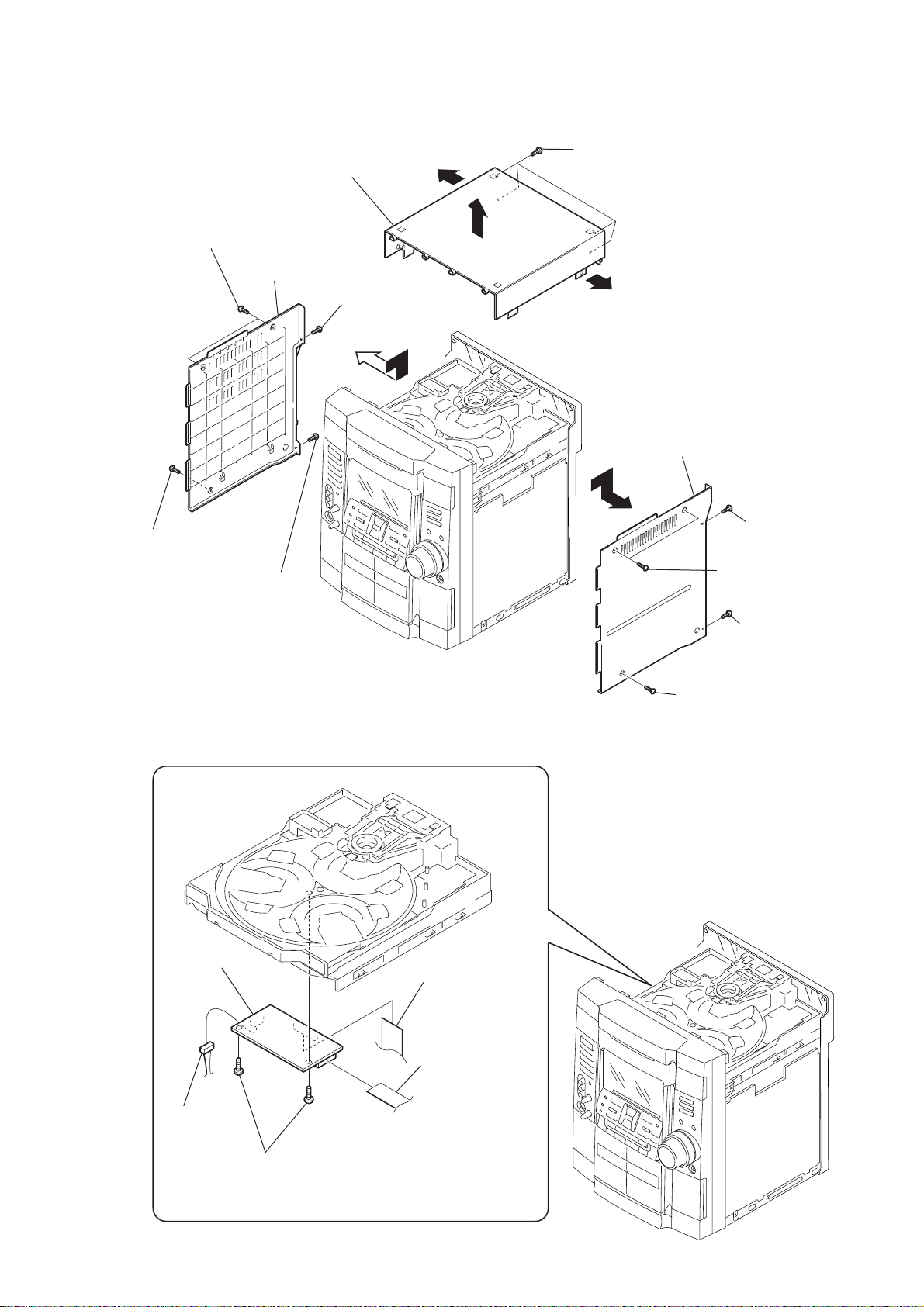
Note : Disassemble the unit in the order as shown below.
SET
3-1. CASE (TOP)
(Page 9)
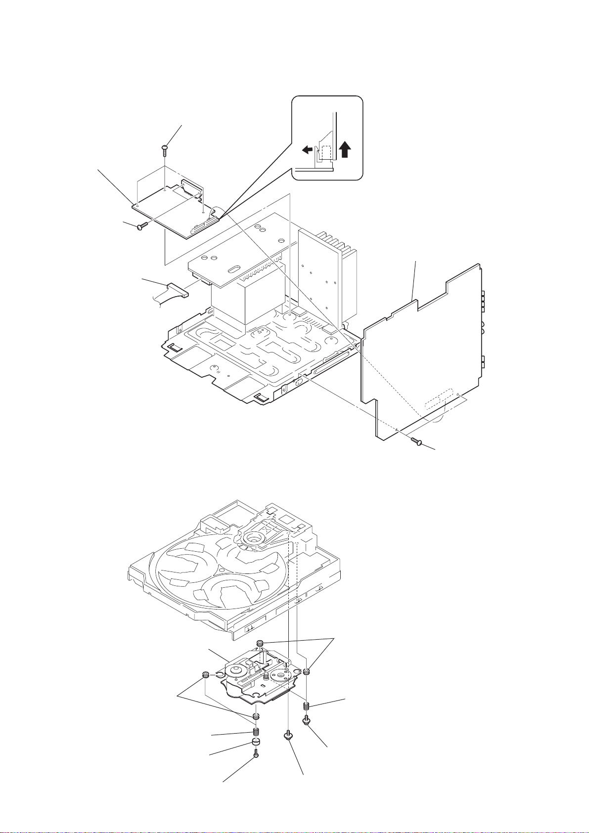
3-2. VIDEO BOARD
(Page 9)
3-3. CD (DOOR)
(Page 10)
3-4. FRONT PANEL SECTION
(Page 11)
SECTION 3
DISASSEMBLY
3-5. TAPE MECHANISM DECK
(Page 12)
3-6. PANEL BOARD
(Page 12)
3-7. KEY BOARD
(Page 13)
3-8. SENSOR BOARD
3-10. BASE UNIT
(Page 14)
DC FAN (FAN961)
(Page 13)
3-11. DRIVER BOARD,
MOTOR BOARD,
SENSOR (CD) BOARD
(Page 15)
3-9. MAIN BOARD,
POWER AMP BOARD
(Page 14)
8
Note : Follow the disassembly procedure in the numerical order given.
)
HCD-RV2/RV5/RV6
3-1. CASE (TOP)
two screws (case 3 TP2)
7
8
screw (case 3 TP2)
qs
0
screw
(+BVTT 3
qg
case (side-L)
9
(+BVTP 3
×
8)
case (top)
screw
qd
four screws (+BVTP 3
qf
×
10)
qa
5
×
10)
6
case (side-R)
1
(case 3 TP2)
3
screw
(+BVTP 3
two screws
×
10
3-2. VIDEO BOARD
5
VIDEO board
2
3
CN101
CN201
(flat type)
(flat type)
4
(+BVTT 3
2
screw (case 3 TP2)
screw
×
8)
1
CN301
4
two screws (+BVTP 3
×
10)
9

HCD-RV2/RV5/RV6
3-3. CD (DOOR)
CD mechanism deck (CDM58F)
1
Turn the pulley to the direction of arrow.
Front panel side
4
CD door
pulley
2
Pull-out the disc tray.
3
10
3-4. FRONT PANEL SECTION
qf
CD mechanism deck (CDM58E)
6
screw
(+BVTP 3
×
10)
qs
5
screw
(+BVTP 3
2
×
10)
qd
CN103
CN671
(flat type)
1
HCD-RV2/RV5/RV6
CN685
9
8
three screws (+BVTP 3
×6
0
3
qa
front panel section
)
7
(+BVTP 3
connector 6p
screw
×
10)
4
connector 3p
11
HCD-RV2/RV5/RV6
)
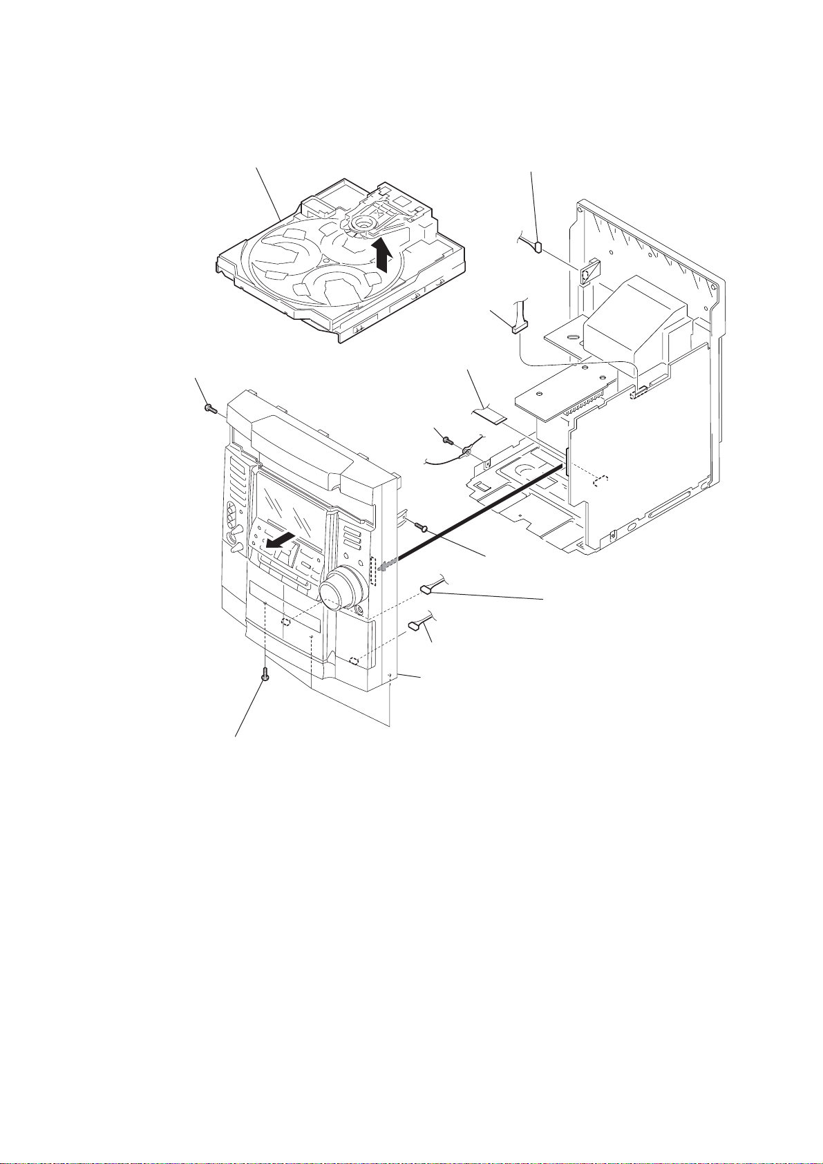
3-5. TAPE MECHANISM DECK
2
tape mechanism deck
1
six
screws
(+BVTP 2.6
×
8
3-6. PANEL BOARD
claws
2
CN704
6
PANEL board
7
CN712
claws
3
three
(+BVTP 2.6
screws
×
8)
4
(+BVTP 2.6
5
(+BVTP 2.6
six
two
screws
screws
×
8)
×
8)
12
1
volume knob

3-7. KEY BOARD
claw
3
two
screws
(+BVTP 2.6
2
(+BVTP 2.6
4
KEY board
×
8)
two
screws
1
two
screws
(+BVTP 2.6
HCD-RV2/RV5/RV6
×
8)
×
8)
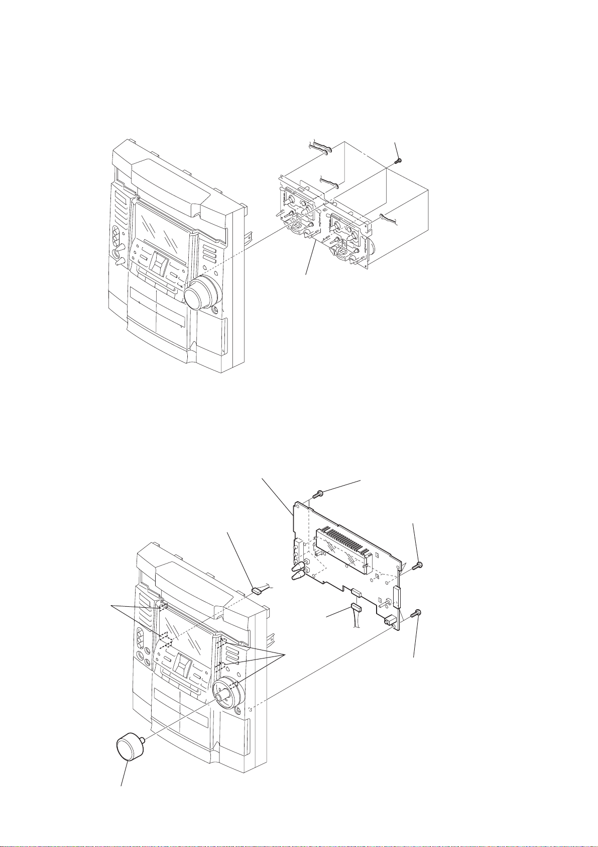
3-8. SENSOR BOARD, DC FAN (FAN961)
8
cover (duct)
0
SENSOR board
9
screw
(+BVTP 2.6
×
4
8)
CN504
1
CN901
3
CN903
5
2
CN304
CN2
qd
6
CN305
7
two screws
(+BVTP 3
qs
(+BVTP 3
qf
×
10)
six screws
qg
(+BVTP 3
qa
(+BVTT 3
panel back
two screws
two screws
×
10)
×
16)
×
6)
qh
DC fan (FAN961)
13
HCD-RV2/RV5/RV6
3-9. MAIN BOARD, POWER AMP BOARD
4
three
(+BVTP 3
6
POWER AMP board
5
two
screws
×
(+BVTP 3
16)
1
CN915
screws
×
10)
MAIN board
3
MAIN board
3-10. BASE UNIT
8
two insulators
6
two
coil springs (insulator)
5
two stoppers (BU)
7
base unit
9
two insulators
3
two
coil springs (insulator)
2
two
screws (+PTPWH M2.6)
2
two
screws
(+BVTP 3
×
10)
14
4
two screws (+BVTP 2.6
1
×
8)
screw (DIA. 12)
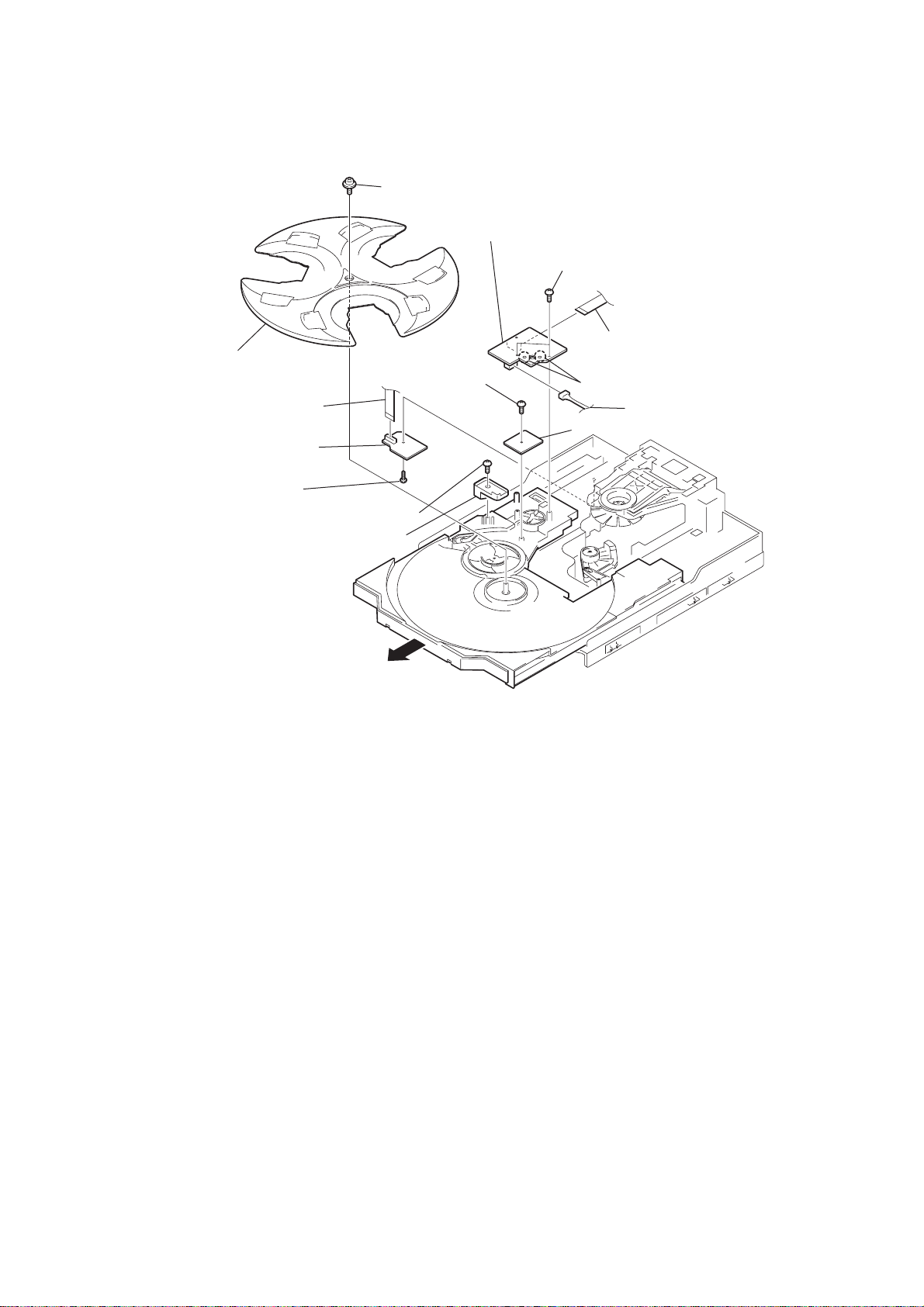
3-11. DRIVER BOARD, MOTOR BOARD, SENSOR (CD) BOARD
qs
qd
tray
3
CN702 (flat type)
2
DRIVER board
1
screw
(+BVTP 2.6
×
8)
4
screw (+BVTP 2.6
5
stopper (tray)
screw (+PTPWH 2.6
0
qf
screw
(+BVTP 2.6
×
8)
×
8)
MOTOR board
×
8)
HCD-RV2/RV5/RV6
6
two screws (+BVTP 2.6
8
CN721(flat type)
7
Remove the two solderings of motor.
9
CN722
qg
SENSOR (CD) board
×
8)
qa
Pull-out the disc tray.
15

HCD-RV2/RV5/RV6
)
4-1. CIRCUIT BOARDS LOCATION
SECTION 4
DIAGRAMS
VIDEO board
TRANS board
PANEL board
REMOTE board
MIC board
KEY board
SENSOR (CD) board
DRIVER board
MOTOR board
VIDEO OUT board
SENSOR board
(HCD-RV5/RV6)
BD board
SUB TRANS board
SURROUND board
(HCD-RV6
MAIN board
POWER AMP board
16

HCD-RV2/RV5/RV6
THIS NOTE IS COMMON FOR PRINTED WIRING
BOARDS AND SCHEMATIC DIAGRAMS.
(In addition to this, the necessary note is
printed in each block.)
for schematic diagram:
• All capacitors are in µF unless otherwise noted. pF: µµF
50 WV or less are not indicated except for electrolytics
and tantalums.
• All resistors are in Ω and 1/
specified.
•%: indicates tolerance.
f
•
• C : panel designation.
Note: The components identified by mark 0 or dotted line
• A : B+ Line.
• B : B– Line.
• H : adjustment for repair.
•Voltage and waveforms are dc with respect to ground
•Voltages are taken with a VOM (Input impedance 10 MΩ).
• BD section
• VIDEO (1/2), (2/2), MAIN (1/4), (2/4), (3/4), (4/4), P ANEL,
•Waveforms are taken with a oscilloscope.
• Circled numbers refer to waveforms.
• Signal path.
• Abbreviation
: internal component.
with mark 0 are critical for safety.
Replace only with part number specified.
under no-signal (detuned) conditions.
Voltage variations may be noted due to normal produc-
tion tolerances.
no mark : CD
POWER sections.
no mark : FM
(): CD
[]: TAPE
Voltage variations may be noted due to normal production tolerances.
F : FM
f : AM
E : PB (DECK A)
d : PB (DECK B)
G : REC (DECK B)
J : CD
L : VIDEO
E3 : 240 V AC area in E model
EA : Saudi Arabia model
MY : Malaysia model
SP : Singapore model
TH : Thai model
4
W or less unless otherwise
•Waveforms
– BD Board –
1
IC103
6
2
IC103
7
3
IC103
qg
4
IC103
wk
Approx.
160mVp-p
(A), 8 (C)
Approx.
160mVp-p
(B), 9 (D)
Approx.
1Vp-p
(RFAC)
Approx.
0.6Vp-p
(RFDCO)
– VIDEO Board –
1
33.8688MHz
IC505
(XTAO)
<zb/>
2
29MHz
IC505
(CLKA)
<x/n>
1.1Vp-p
0.6Vp-p
– MAIN Board –
1
4.5MHz
1
(XIN)
IC102
2
32.768kHz
IC601
(XCOUT)
qa
3
16MHz
IC601
(XOUT)
qd
– PANEL Board –
1
5MHz
IC701
3
1.8Vp-p
2.8Vp-p
0.6Vp-p
3Vp-p
(X1)
for printed wiring boards:
• X : parts extracted from the component side.
• Y : parts extracted from the conductor side.
• x : parts mounted on the conductor side.
• : Pattern from the side which enables seeing.
(The other layer’s patterns are not indicated.)
Caution:
Pattern face side: Parts on the pattern face side seen from the
(Side B) pattern face are indicated.
Parts face side: Parts on the parts face side seen from the
(Side A) parts face are indicated.
• Abbreviation
E3 : 240 V AC area in E model
EA : Saudi Arabia model
MY : Malaysia model
SP : Singapore model
TH : Thai model
17 17
HCD-RV2/RV5/RV6
4-2. PRINTED WIRING BOARD — BD SECTION — • Refer to page 16 for Circuit Boards Location.
A
B
C
D
E
F
1
234567891011 12 13 14
M101
C163
C182
C166
C164
C165
C153
R228
C101
R227
R126
C102
R229
C104
C109
C112
C103
R117
C120
C111
C115
C108
C117
R113
R109
R102
R105
R111
Q102
C110
R103
R118
R114
R179
R176
R104
C107
R120
R112
IC103
C213
R226
R152
C151
R235
IC102
R151
R236
R231
CN101
(Page 22)
G
H
R125
C114
I
• Semiconductor
C119
C113
R122
R123
Q101
R124
R234
C118
CN102
M102
Location
Ref. No. Location
IC102 C-12
IC103 F-9
Q101 G-9
Q102 C-9
1818
• Refer to page 17 for Waveforms.
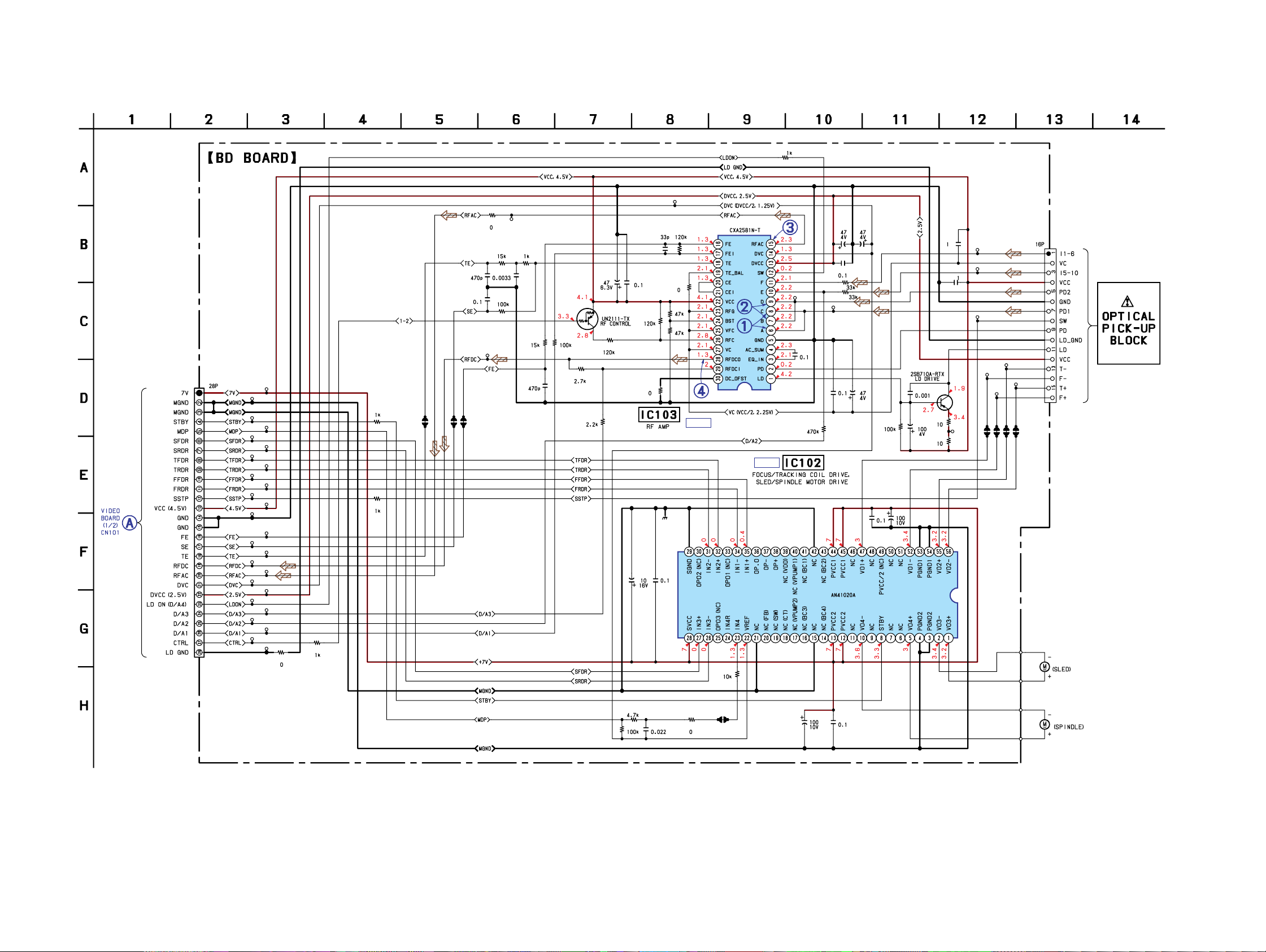
4-3. SCHEMATIC DIAGRAM — BD SECTION — • Refer to page 52 for IC Block Diagrams.
TP49
C213
R105
R102
C104C101
C102
R103
R104
C103
(Page 24)
CN101
TP56
TP57
TP58
TP59
TP60
TP61
TP62
TP63
TP64
TP65
TP66
TP67
TP69
TP70
TP71
TP72
TP73
TP74
TP75
TP76
TP77
TP78
TP79
TP80
TP55
TP68
R234
R226
R236
R235
TP17
TP18
TP21
TP19
R227
R113
R229
C115
R109
Q102
C117
C165
R111
R118
TP27
C107
C153
R120
R112
R114
R117
IC B/D
R179
IC103
R231
IC B/D
TP24
C110
R228
R126
R125
C112
C109
TP23
C108
IC102
C120
C111
C166
R122
C182
C114
C113
Q101
R124
R123
C118
C119
TP22
TP26
TP25
TP54
TP16
TP53
TP52
TP15
TP14
HCD-RV2/RV5/RV6
CN102
TP51
TP50
TP13
M102
R152
R151
C151
R176
19 19
TP100
C163
C164
M101

HCD-RV2/RV5/RV6
4-4. PRINTED WIRING BOARDS — CD SECTION — • Refer to page 16 for Circuit Boards Location.
A
B
C
12
MOTOR BOARD
3456
SENSOR (CD) BOARD
IC711
4
14
14
• Semiconductor
Location
Ref. No. Location
D701 F-1
IC701 E-1
IC711 B-5
D
E
14
14
DRIVER BOARD
IC701
F
G
C
CN103
14
14
(Page 30)
2020
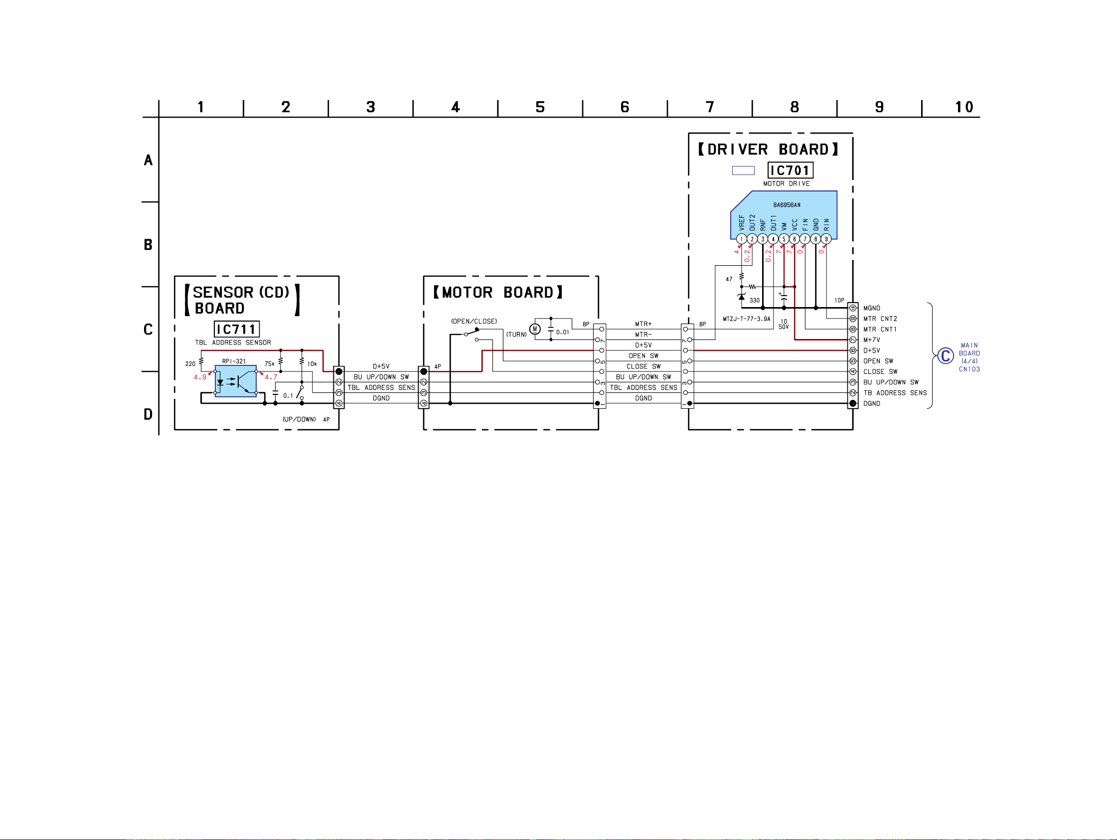
4-5. SCHEMATIC DIAGRAM — CD SECTION — • Refer to page 52 for IC Block Diagram.
HCD-RV2/RV5/RV6
IC B/D
IC701
R702
R712
IC711
R711 R713
C712
S711
CN711
CN722
S701
M721
C721
CN721
CN702
D701
R701
CN701
C702
(Page 29)
21 21

HCD-RV2/RV5/RV6
4-6. PRINTED WIRING BOARD — VIDEO SECTION — • Refer to page 16 for Circuit Boards Location.
A
B
C
D
E
F
G
1
(Page 31)
(Page 34)
(Page 37)
234567891011121314
EP200
R102
C258
C115
R115
R114
R152
L102
IC102
EP202
CN201
(Page 30)
C366
CN301
C365
JW523
R309
IC508
R310
C309
524
JW
R307R308
C308
IC302
C307
C305
C573
C301
R301
R303
IC301
R305
R302
R318
C315
IC303
IC505
C324
R323
C325
IC304
R324
C502
C326
C524
C503
R502
FB501
C570
C584
C501
C551
R558
C544
R501
R551
C582
C597
C552
R552
C540
RV501
C538
C543
C596
R557
R556
R555
R554
C114
R202
C209
H
J
C567
C561
C568
EP201
203
JW
R533
CN101
FB252
C525
FL201
C211
C214
C212
C210
IC202
I
• Semiconductor Location
Ref. No. Location
IC102 C-13
(IC201) I-13
IC202 H-13
IC301 C-6
IC302 C-5
( ) : SIDE B
Ref. No. Location Ref. No. Location Ref. No. Location
IC303 C-8
IC304 C-9
(IC307) C-3
(IC504) C-10
IC505 F-8
(IC506) H-4
(IC507) F-5
IC508 F-5
(Q201) G-11
(Q301) C-8
(Q302) B-5
(Q370) D-2
(Q581) B-10
(Page 18)
2222

HCD-RV2/RV5/RV6
EP202
C116
C201
C202
R108
C156
C106
C259
R507
R506
R505
R504
R503
C105
R109
R159
R508
FB201
R102
C213
R107
R158
FL503
FB503
C221
R157
C205
C208
C154
C206
C547
Q201
R201
C596
IC504
C207
C581
FB502
C583
FL504
FB504
X502
Q581
C222
C321
R321
C545
C204
R581
C339
R549
C534
C537
C322
C549
C541
R582
C338
C542
R550
C539
R534
R559
C548
C327
C329
R326
C323
C546
R548
C533
L321
C328
L322
R522
R547
C536
R544
R322
R546
R327
C504
Q301
R545
R325
C535
R543
R532
R509
R513C550
R316
C311
R542
C317
R314
R511
R541
C318
R317
R311
R510
R315
C312
L311
R538
R512
C523
C505
C510
C314
R312
C313
C521
C303
C522
C513
X501
R306
FL501
C511
C575
C302
L301
C572
FB561
JW301
C566
C363
IC507
Q302
R372
R373
IC506
C360
C571
FB360
FL502
C576
C361
IC307
R376
R374
R375
Q370
C364
234567891011121314
1
A
B
C
D
E
F
G
H
IC201
C203
C257
C224
C255
C223
C254
FB251
R531
C574R561
I
J
23 23
HCD-RV2/RV5/RV6
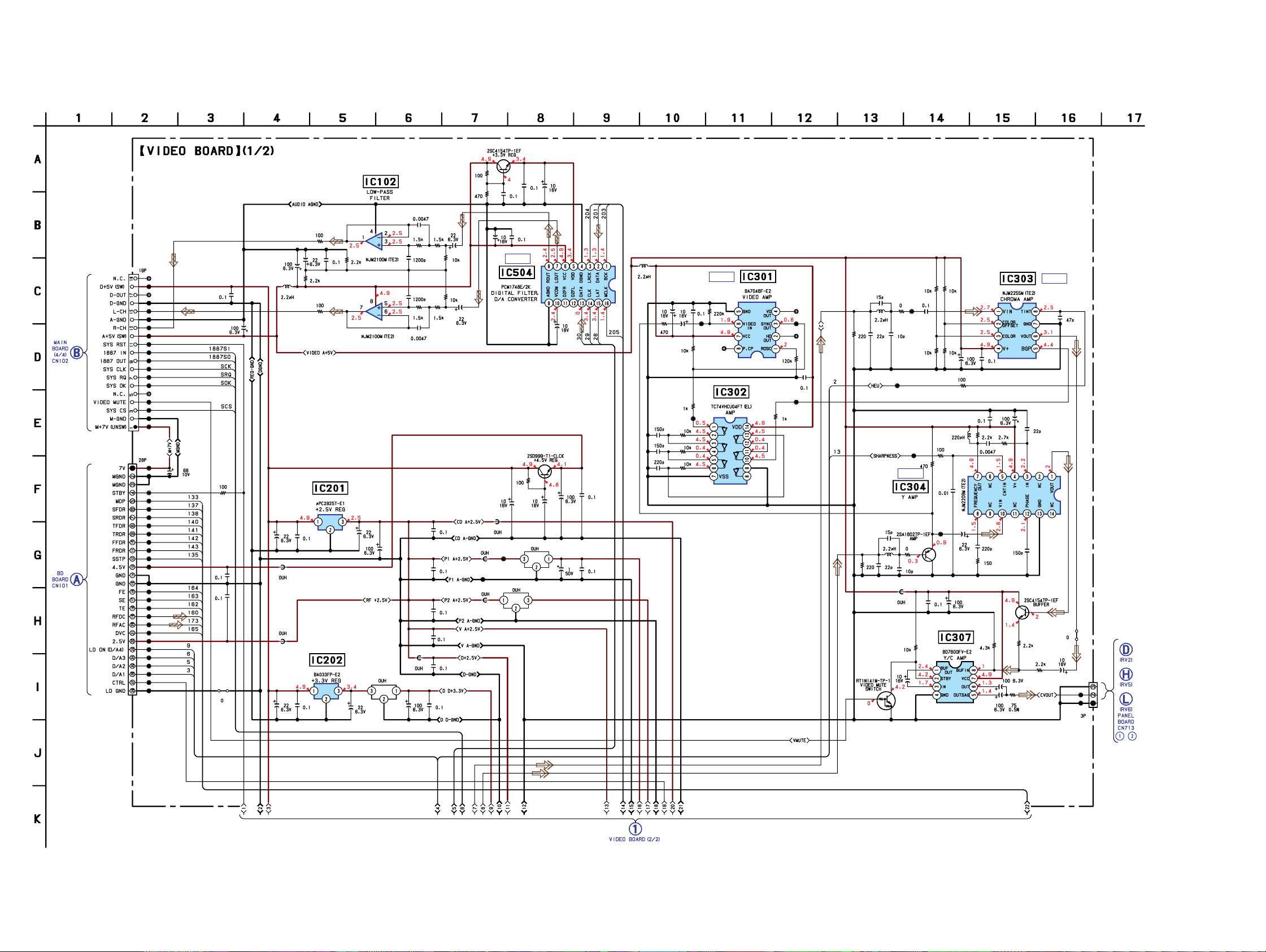
4-7. SCHEMATIC DIAGRAM — VIDEO SECTION (1/2) — • Refer to page 52 for IC Block Diagrams.
Q581
(Page
29)
(Page
19)
CN201
CN101
TP419
TP418
TP417
TP416
TP415
TP414
TP413
TP412
TP411
TP410
TP409
TP408
TP407
TP406
TP405
TP404
TP403
TP402
TP401
TP421
TP422
TP424
TP425
TP426
TP427
TP428
TP429
TP430
TP431
TP432
TP433
TP434
TP436
TP437
TP438
TP439
TP440
TP441
TP442
TP443
TP444
TP445
TP446
TP447
TP448
C257
C258
C255
C254
JW203
R202
C259
C201
FB252
FB251
C209
C116
L102
C202
C210
C114
R114
R152
R102
IC202
IC201
C115
R115
C214
IC102(1/2)
IC102(2/2)
C213
C203
FL201
C155
R159
C156
C106
R109
C105
FB201
C211
R158
R108
C212
C204
C205
C206
C207
C208
C154
R157
R107
C104
R581
R582 C584
C596
IC B/D
C221
FB501
FB503
TP197
TP198
FB502
IC504
FL504
C581
R201
C583
C222
FL503
Q201
C582
C597
C223
C547
C224
C548
L301
C307
C308
C309
C301
R302
R307
R308
R309
C303
R305
R306
TP304
C302
TP312
IC B/D
R301
TP313
IC302
IC301
R303
R310
TP311
TP309
TP305
TP310
C305
R321
Q370
C312
L311
C322
C321
L321
R312
C313C311R311
TP302
FB360
C364
TP301
TP306
IC B/D
TP303
Q301
R322
C323
R376
R323
R316
C314
R317
R327
C361
C329
R314
R315
L322
C360
IC307
R318
4
30
IC
C324
C318
C338
C328
C325
R374
C317
R324
R325R326
C366
C339
C326
C365
R375
IC303
R372
C327
Q302
R373
IC B/D
C363
C315
JW301
TP308
TP307
(Page 33)
(Page 36)
(Page 39)
CN301
(Page 25)
2424
• Refer to page 17 for Waveforms.
4-8. SCHEMATIC DIAGRAM — VIDEO SECTION (2/2) — • Refer to page 53 for IC Block Diagram.
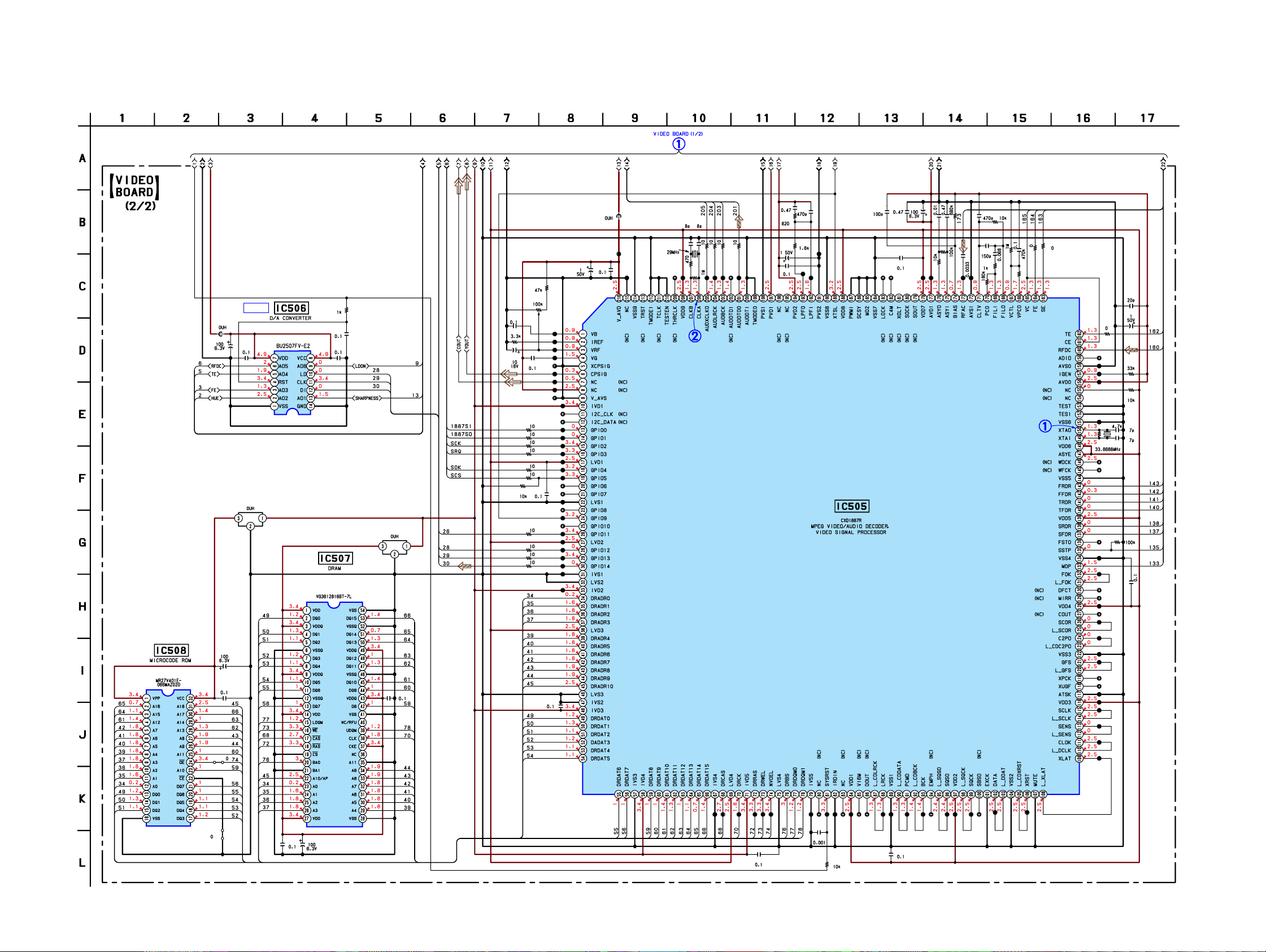
HCD-RV2/RV5/RV6
(Page 24)
IC508
C566
JW524
FB561
C575
C573
IC B/D
C561
FL501
IC506
IC507
R561
C574
C567
FL502
C572
C502
R502
C501
R503
R504
R505
R506
R507
R508
R509
R510
R511
R512
R513
RV501
C503
R501
C504
C544
FB504
TP216
C552
C551
TP215
TP1
TP2
TP3
TP4
TP5
TP6
TP7
TP8
TP9
TP10
TP11
TP12
TP13
TP14
TP15
TP16
TP17
TP18
TP19
TP20
TP21
TP22
TP23
TP24
TP25
TP26
TP27
TP28
TP29
TP30
TP31
TP33
C505
X502
TP209
C550 C549
TP208
559
R
57
554
555
R
R5
R
R556
05
202
204
P201
TP203
TP2
T
TP
TP
558
R
R552
C545
C546
C543
R551
TP193
TP191
TP192
C537
IC505
C538C540
539
C
C541
7
C542
183
TP
TP182
TP178
TP17
550
R
C534
C570
R547
C536
544
R
R545
72
TP1
C535
R546
R541
542
533
R
C
543
R
C524
C525
R534
TP159
TP158
R533
TP157
TP156
R538
TP151
C523
R532
C522
X501
TP146
TP145
R531
TP136
TP134
TP132
TP130
TP129
TP128
TP127
TP126
TP124
TP122
TP121
TP119
TP118
TP117
TP116
TP115
TP113
TP111
TP109
521
C
548
R
73
549
R
TP1
JW523
C571
C576
25 25
80
P67
T
TP68
TP70
TP72
C510
TP73
TP74
TP79
C513
82
P81
T
TP
TP
TP83
R522
TP84
88
86
85
TP89
TP
TP
TP
TP91
C511
TP93
6
P94
P97
TP9
T
T
2
99
TP
TP100
TP10
TP106
HCD-RV2/RV5/RV6
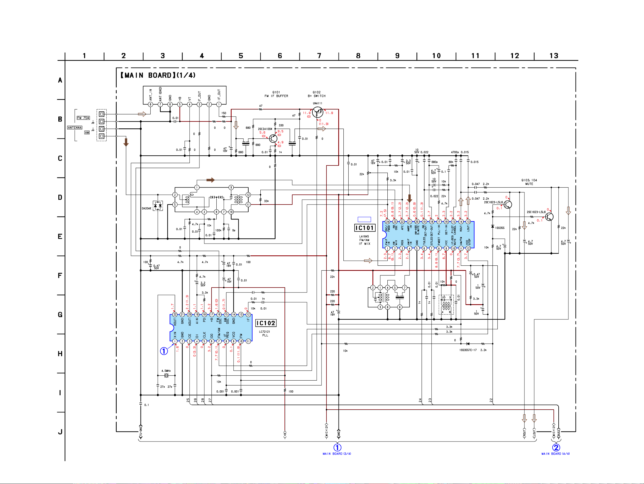
4-9. SCHEMATIC DIAGRAM — MAIN SECTION (1/4) — • Refer to page 54 for IC Block Diagram.
• Refer to page 17 for Waveform.
FE101
JK101
D101
C113
C100
C101
C112
JR112
R112R111
JR105
JR104
R113
C111
R114
R135
C116
R136
JR106 JR107
JR108
RB101
R115
C110
R104
C104
R117 C109
C114
C117
R106
C115
R102
CF101
R116
C118
R101
Q101
R103
R142
R121
C119
R122 C120
JR111
R108
R105C102
CF102
R109
C105
Q102
JR110
R120
R141
R124
C125
C128
RV101
IC B/D
IC101
C106
IFT101
C107
R140
R110
C108
C148
C143
C147
R147
C139
C138
C140
C146
C129
R148
R125
C130
C141
R131
R139
R132
T101
C142 C132
JR114
C126
C131R137
C151 R129
C150 R128
R138
C133
C127
R127
C137
R144
Q104
D109
C144
R134
R143
C136
Q103
R133
C135
C360
X101
IC102
R123
JR113
C122C121
R119
C123 C124
R118
(Page 28)
R146
R130
JR116
D108
R126
(Page 29)
2626
 Loading...