

Page 1
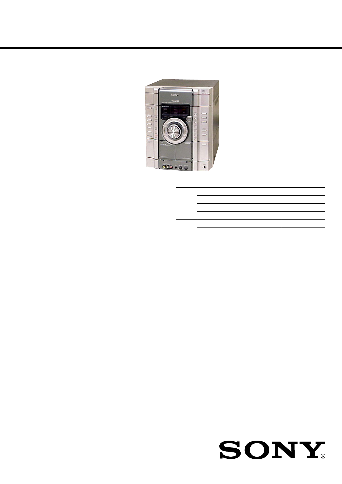
HCD-RV555
SERVICE MANUAL
Ver. 1.2 2008.02
• HCD-RV555 is the tuner, deck, CD
and amplifier section in MHC-RV555.
CD
Section
TAPE
Section
E Model
Model Name Using Similar Mechanism HCD-RV55
CD Mechanism Type CDM74KS-KBD49
Base Unit Name BU-K4BD49
Optical Pick-up Name KSM-213DHAP
Model Name Using Similar Mechanism HCD-RV55
Tape Mechanism Type CWM43RR602
Amplifier section
The following measured at AC 120, 127, 220, 240 V
50/60 Hz
DIN power output (rated): 120 + 120 watts
(6 ohms at 1 kHz, DIN)
Continuous RMS power output (reference):
150 + 150 watts
(6 ohms at 1 kHz, 10% THD)
Inputs
VIDEO/SAT IN (phono jacks):
voltage 450/250 mV,
impedance 47 kilohms
GAME INPUT AUDIO L/R (phono jacks):
voltage 250 mV,
impedance 47 kilohms
GAME INPUT VIDEO (phono jack):
1 Vp-p, 75ohms
MIC (phone jack): sensitivity 1 mV,
impedance 10 kilohms
SPECIFICATIONS
Outputs
PHONES (stereo mini jack): accepts headphones of
8 ohms or more
VIDEO OUT (phono jack): max. output level 1 Vp-p,
unbalanced, Sync negative
load impedance 75 ohms
VIDEO/SAT OUT (phono jacks)
impedance 1 kilohm
SPEAKER: accepts impedance of 6 to
16 ohms
CD player section
System Compact disc and digital
audio system
Laser Semiconductor laser
(λ=770 – 810 nm)
Emission duration:
continuous
Frequency response 2 Hz – 20 kHz (±0.5 dB)
Signal-to-noise-ratio More than 90 dB
Dynamic range More than 90 dB
Video color system format NTSC, PAL
– Continued on next page –
9-887-231-03
2008B04-1
© 2008.02
MINI Hi-Fi COMPONENT SYSTEM
Sony Corporation
Audio Business Group
Published by Sony Techno Create Corporation
Page 2

HCD-RV555
Tape deck section
Recording system 4-track 2-channel, stereo
Frequency response 50 – 13,000 Hz (±3 dB),
Tuner section
FM stereo, FM/AM superheterodyne tuner
FM tuner section
Tuning range 87.5 – 108.0 MHz
Antenna FM lead antenna
Antenna terminals 75 ohms unbalanced
Intermediate frequency 10.7 MHz
AM tuner section
Tuning range 530 – 1,710 kHz
Antenna AM loop antenna
Antenna terminals External antenna terminal
Intermediate frequency 450 kHz
using Sony TYPE I cassettes
(50 kHz step)
(with the tuning interval
set at 10 kHz)
531 – 1,602 kHz
(with the tuning interval
set at 9 kHz)
General
Power requirements 120 V, 220 V or
Power consumption 155 watts
Dimensions (w/h/d) incl.projecting parts and controls
Amplifier/Tuner/Tape/CD Section:
Mass Approx. 10.6 kg
Supplied accessories: Remote Commander (1)
Design and specifications are subject to change without
notice.
230 – 240 V AC, 50/60 Hz
Adjustable with voltage
selector
Approx. 280 × 327 × 425 mm
R6 (Size AA) batteries (2)
AM loop antenna (1)
FM lead antenna (1)
Speaker pads (8)
Video cable (1)
SAFETY-RELATED COMPONENT WARNING!!
COMPONENTS IDENTIFIED BY MARK 0 OR DOTTED LINE
WITH MARK 0 ON THE SCHEMATIC DIAGRAMS AND IN
THE PARTS LIST ARE CRITICAL TO SAFE OPERATION.
REPLACE THESE COMPONENTS WITH SONY PARTS WHOSE
PART NUMBERS APPEAR AS SHOWN IN THIS MANUAL OR
IN SUPPLEMENTS PUBLISHED BY SONY.
2
Page 3
HCD-RV555
Notes on Chip Component Replacement
•Never reuse a disconnected chip component.
• Notice that the minus side of a tantalum capacitor may be
damaged by heat.
Flexible Circuit Board Repairing
•Keep the temperature of soldering iron around 270°C during
repairing.
• Do not touch the soldering iron on the same conductor of the
circuit board (within 3 times).
• Be careful not to apply force on the conductor when soldering or
unsoldering.
UNLEADED SOLDER
Boards requiring use of unleaded solder are printed with the leadfree mark (LF) indicating the solder contains no lead.
(Caution: Some printed circuit boards may not come printed with
the lead free mark due to their particular size.)
: LEAD FREE MARK
Unleaded solder has the following characteristics.
• Unleaded solder melts at a temperature about 40°C higher than
ordinary solder.
Ordinary soldering irons can be used but the iron tip has to be
applied to the solder joint for a slightly longer time.
Soldering irons using a temperature regulator should be set to
about 350°C.
Caution: The printed pattern (copper foil) may peel away if the
heated tip is applied for too long, so be careful!
• Strong viscosity
Unleaded solder is more viscous (sticky, less prone to flow) than
ordinary solder so use caution not to let solder bridges occur such
as on IC pins, etc.
• Usable with ordinary solder
It is best to use only unleaded solder but unleaded solder may
also be added to ordinary solder.
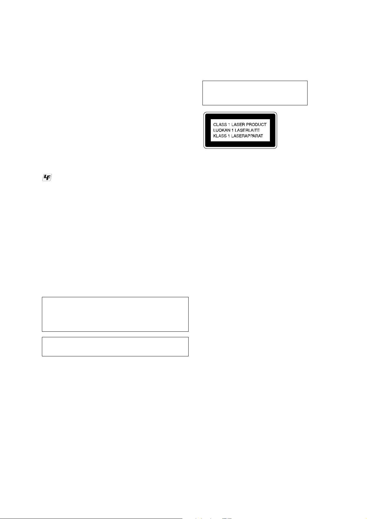
NOTES ON LASER DIODE EMISSION CHECK
The laser beam on this model is concentrated so as to be focused on
the disc reflective surface by the objective lens in the optical pickup block. Therefore, when checking the laser diode emission,
observe from more than 30 cm away from the objective lens.
Laser component in this product is capable
of emitting radiation exceeding the limit for
Class 1.
This appliance is
claassified as a CLASS 1
LASER product. This
label is located on the
rear exterior.
CAUTION
Use of controls or adjustments or performance of procedures
other than those specified herein may result in hazardous
radiation exposure.
NOTES ON HANDLING THE OPTICAL PICK-UP BLOCK
OR BASE UNIT
The laser diode in the optical pick-up block may suffer electrostatic
breakdown because of the potential difference generated by the
charged electrostatic load, etc. on clothing and the human body.
During repair, pay attention to electrostatic breakdown and also use
the procedure in the printed matter which is included in the repair
parts.
The flexible board is easily damaged and should be handled with
care.
3
Page 4
HCD-RV555
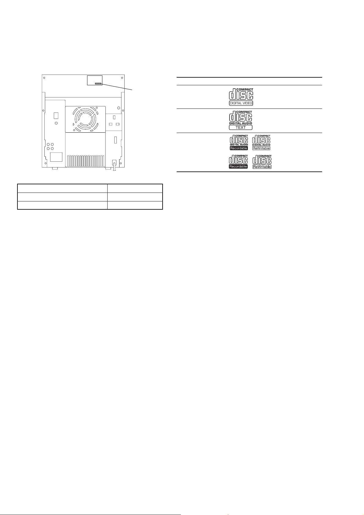
MODEL IDENTIFICATION
– MODEL NUMBER LABEL –
Par t No.
MODEL PARTS No.
RV555: E3, E15 2-685-237-0s
RV555: SP 2-685-238-0s
•Abbreviation
E3 : 240 V AC area in E model
E15 : Iran model
SP : Singapore model
PLAYABLE DISC
You can playback the following discs on this system. The other
discs cannot be played back.
List of playable discs
Format of discs Disc logo
VIDEO CDs
Audio CDs
CD-R/CD-RW
(audio data/MP3
files)
4
Page 5

TABLE OF CONTENTS
HCD-RV555
1. SERVICE NOTES
1-1. Service Position of CD Mechanism Deck ....................... 6
1-2. Service Position of Amp Board ....................................... 6
2. GENERAL
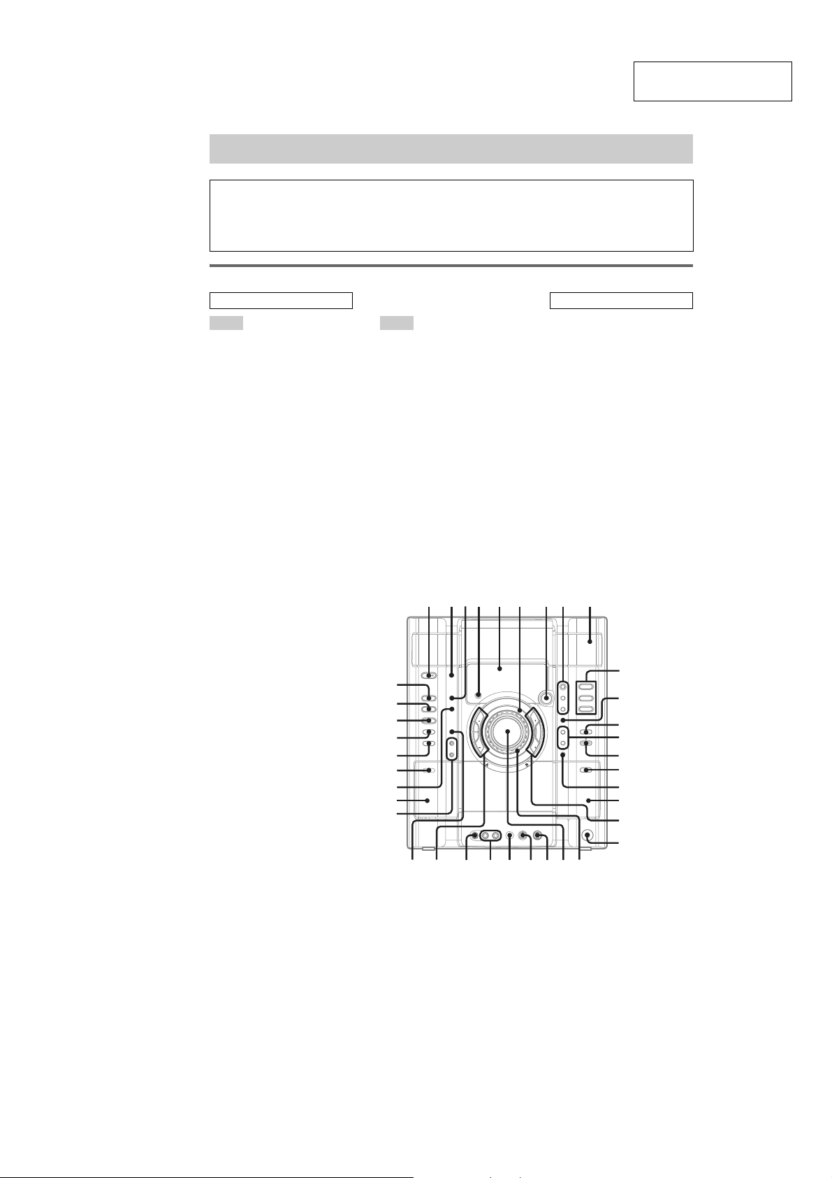
List of Button Locations and Reference Pages ............... 7
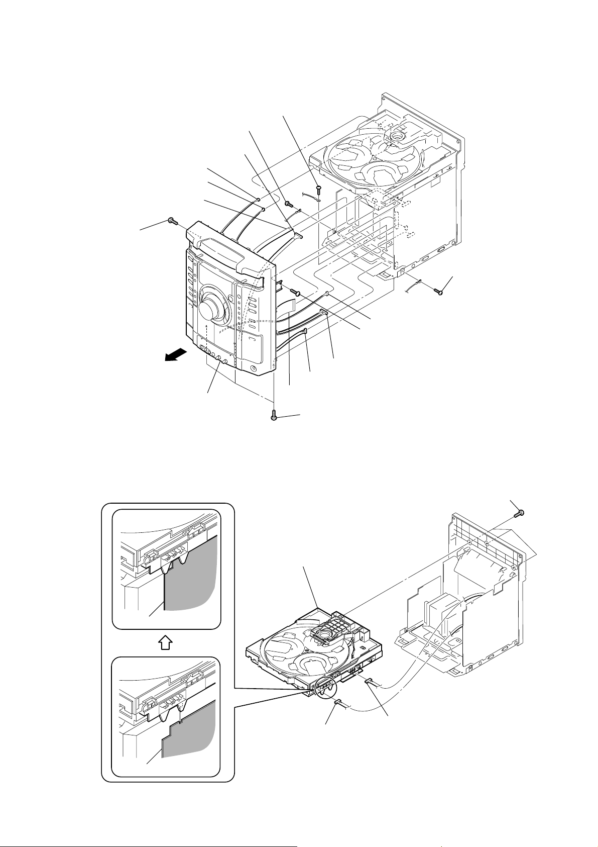
3. DISASSEMBLY
3-1. Case (Top) ....................................................................... 10
3-2. CD Door .......................................................................... 10
3-3. Front Panel Section ......................................................... 11
3-4. CD Mechanism Deck ...................................................... 11
3-5. Tape Mechanism Deck, Microphone Jack Board ............ 12
3-6. Panel Board ..................................................................... 12
3-7. Back Panel Section, Sub Transformer Board .................. 13
3-8. Transformer Board .......................................................... 13
3-9. Main Board ...................................................................... 14
3-10. Amp Board ...................................................................... 14
3-11. BD Board ......................................................................... 15
3-12. VCD Connect Board, VMP Board .................................. 15
3-13. Driver Board, SW Board ................................................. 16
3-14. Base Unit ......................................................................... 16
3-15. Sensor Board ................................................................... 17
3-16. Motor (TB) Board ........................................................... 17
3-17. Motor (LD) Board ........................................................... 18
4. TEST MODE ............................................................... 19
5. ELECTRICAL ADJUSTMENTS .......................... 23
6. DIAGRAMS
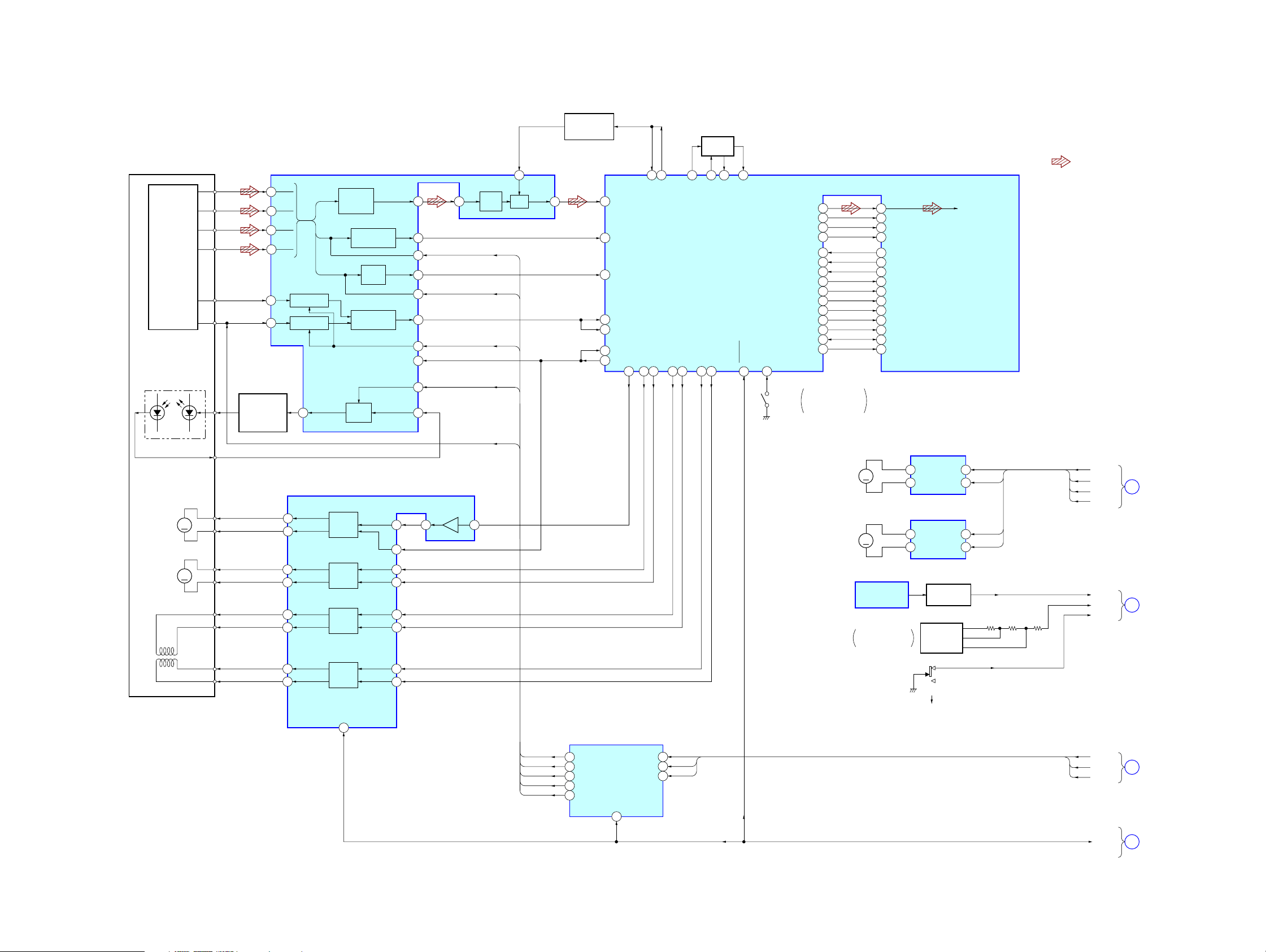
6-1. Block Diagram –CD Servo Section– ............................... 25
6-2. Block Diagram –Audio/Video CD Section– ................... 26
6-3. Block Diagram –Main Section– ...................................... 27
6-4. Block Diagram –Panel/Power Supply Section– .............. 28
6-5. Circuit Boards Location .................................................. 29
6-6. Printed Wiring Board –CD Mechanism Section (1/2)–... 32
6-7. Schematic Diagram –CD Mechanism Section (1/2)– ..... 33
6-8. Printed Wiring Boards –CD Mechanism Section (2/2)– .. 34
6-9. Schematic Diagram –CD Mechanism Section (2/2)– ..... 35
6-10. Printed Wiring Board –VCD Connect Section– .............. 36
6-11. Schematic Diagram –VCD Connect Section– ................. 36
6-12. Printed Wiring Board –VMP Section– ............................ 37
6-13. Schematic Diagram –VMP Section (1/2)– ...................... 38
6-14. Schematic Diagram –VMP Section (2/2)– ...................... 39
6-15. Schematic Diagram –Main Section (1/2)– ...................... 40
6-16. Schematic Diagram –Main Section (2/2)– ...................... 41
6-17. Printed Wiring Board –Main Section– ............................ 42
6-18. Printed Wiring Boards –Panel Section– .......................... 43
6-19. Schematic Diagram –Panel Section (1/2)– ...................... 44
6-20. Schematic Diagram –Panel Section (2/2)– ...................... 45
6-21. Printed Wiring Boards –Jack Section– ............................ 46
6-22. Schematic Diagram –Jack Section– ................................ 47
6-23. Printed Wiring Board –Power Section (1/2)– .................. 48
6-24. Printed Wiring Boards –Power Section (2/2)– ................ 49
6-25. Schematic Diagram –Power Section– ............................. 50
7. EXPLODED VIEWS
7-1. Main Section .................................................................... 61
7-2. Front Panel Section (1) .................................................... 62
7-3. Front Panel Section (2) .................................................... 63
7-4. Front Panel Section (3) .................................................... 64
7-5. Main Board Section ......................................................... 65
7-6. CD Mechanism Deck Section (1) .................................... 66
7-7. CD Mechanism Deck Section (2) .................................... 67
7-8. CD Mechanism Deck Section (3) .................................... 68
7-9. Base Unit Section ............................................................ 69
8. ELECTRICAL PARTS LIST .................................. 70
5
Page 6
HCD-R555
k
SECTION 1
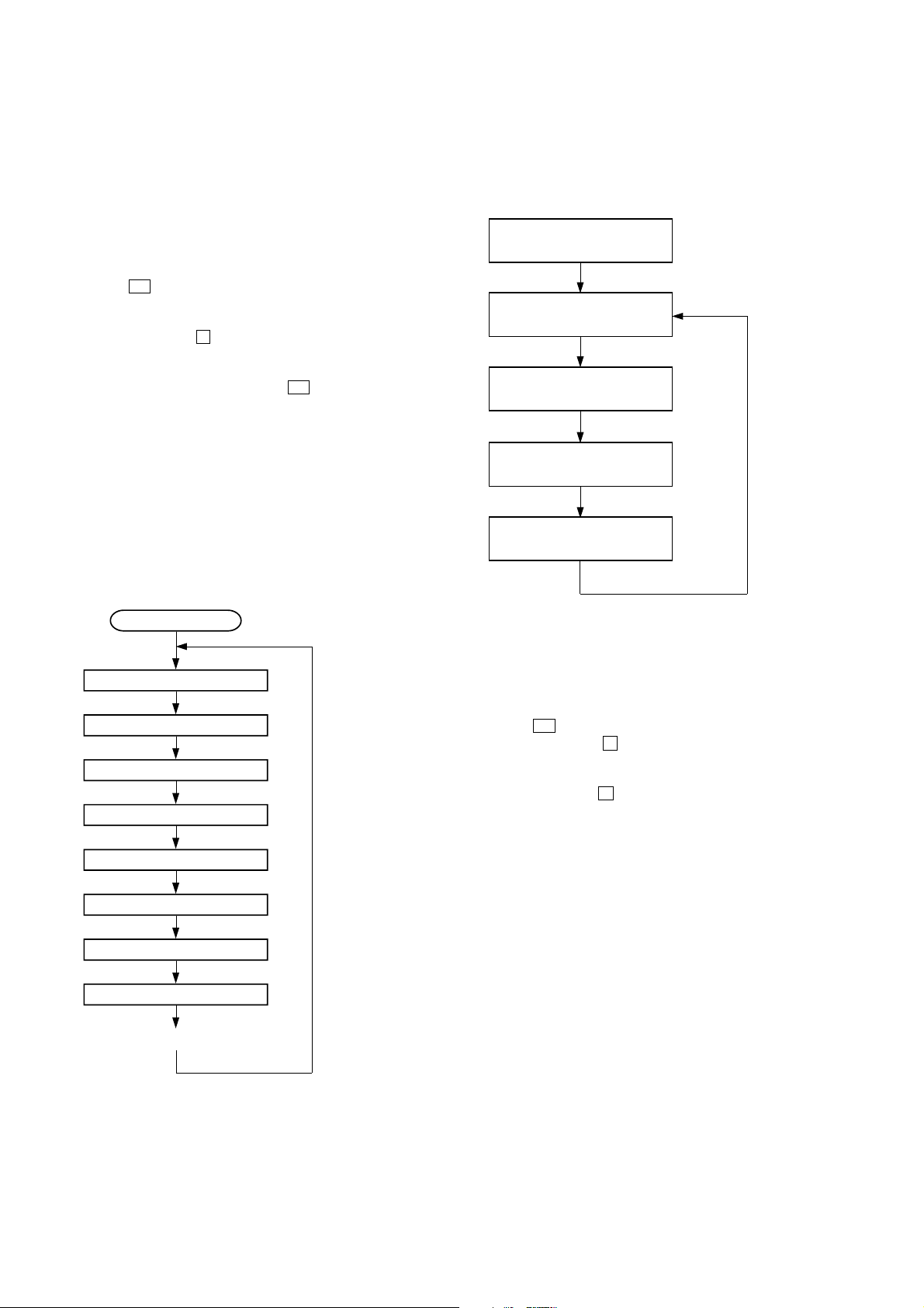
SERVICING NOTES
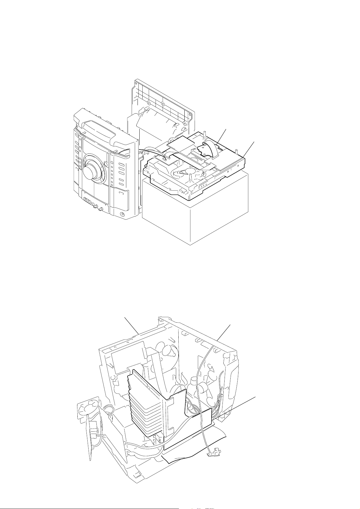
1-1. SERVICE POSITION OF CD MECHANISM DECK
Remove the CD mechanism deck and place it on top of the pedestal as shown.
Inspect the BD board in this set up.
BD board
CD mechanism dec
1-2. SERVICE POSITION OF AMP BOARD
To inspect the POWER board, turn both of the front panel
and the CD mechanism deck so that the left side of the product faces down.
CD mechanism deck
front panel
AMP board
6
Page 7
SECTION 2
Illustrati
w
waw
w
w
w
w
w
GENERAL
List of button locations and reference pages
HCD-RV555
This section is extracted
from instruction manual.
How to use this page
Use this page to find the location of buttons and other
parts of the system that are mentioned in the text.
Main unit
ALPHABETICAL ORDER
A — O P — Z
ALBUM + qk (12, 15, 22)
ALBUM – wj (12, 15, 22)
CD ej (9, 11, 14, 15, 19, 22, 23)
CD SYNC wl (22)
Deck A e; (21)
Deck B qj (21, 22, 23, 27, 29)
DISC 1 – 3 q; (12, 15, 39)
DISC SKIP/EX-CHANGE qs
(11, 12, 15, 22)
Disc tray 9 (11)
DISPLAY 2 (30, 31)
Display window 5
ECHO LEVEL ws (27)
EFFECT ON/OFF 8 (24, 25)
ENTER qa (15, 18, 25)
EQ BAND 7 (25)
GAME ef (23, 25, 35)
GAME INPUT AUDIO L/R jacks
wg (23, 34)
GAME INPUT VIDEO jack wh
(34)
GAME MIXING wk (26)
GROOVE 8 (24)
ILLUMINATION 3 (32)
KARAOKE/MPX qh (26)
MIC jack wf (26)
MIC LEVEL wd (26)
Operation Dial
(–
l L) 6 (
EQ +/
15, 22, 25)
12,
P FILE qd (25)
PHONES jack ql
PLAY MODE ea (12, 15, 21, 22,
23, 27, 39)
Power illuminator w; (32)
PRESET EQ qd (24)
REC PAUSE/ START wl (22, 23,
26, 27)
Remote sensor 4
SURROUND 8 (25)
TAP E A /B eg (21, 22, 23, 27)
TUNER/BAND eh (18, 19, 23)
TUNING MODE ea (18, 19, 39)
TUNING + qk (18, 19)
TUNING – wj (1
VIDEO/SAT* ed (23, 35)
VOLUME control wa
12345 6 78 9
ej
eh
eg
ef
ed
es
ea
e;
wl
8, 19)
j
ALBUM
S
s
TUNING TUNING
on number
r
TA PE A / B eg (21, 22, 23, 27)
Name of button/part Reference page
RR
BUTTON DESCRIPTIONS
?/1 (on/standby) 1 (8, 19, 30,
35, 37, 39)
Z (eject) qf (11)
PUSH Z (deck B) (eject) qg (21)
M (fast forward) qk (8, 12, 22)
H or hH* (play) qk (12, 21,
22)
X (pause) wj (8, 12, 22)
x (stop) wj (12, 22, 27, 39)
m (rewind) wj (8, 12, 22)
Z PUSH (deck A) (eject) es (21)
*MHC-RV555/RV55 only
q;
qa
J
ALBUM
H
h
qs
qd
qf
qg
qh
qj
qk
ql
46
wk
j
GB
g
d
h
f
;
s
7
Page 8
HCD-RV555
Remote control
ALPHABETICAL ORDER
A — M
ALBUM +/– qa (12, 15)
CD wa (11, 15)
CLEAR qj (16)
CLOCK/TIMER SELECT wh
(29, 30)
CLOCK/TIMER SET wh (10, 28,
29)
DISC SKIP q; (12, 15)
DISPLAY 3 (30, 31)
ENTER qs (10, 15, 18, 28, 29)
EQ qh (24)
FM MODE 2 (20)
FUNCTION 4 (11, 14, 15, 18,
19)
KARAOKE/MPX qg (26)
N — Z
NEXT ql (14)
Number buttons w; (13, 14, 16)
ON SCREEN 6 (32)
PLAY MODE wf (12, 15, 21)
PREV ql (14)
REPEAT 2 (15)
SELECT 9
SLEEP wg (28)
SPECIAL MENU 7 (16)
TA PE ws
TUNER BAND 5 (18, 19)
TUNER MEMORY wd (18)
TUNING MODE wf (18, 19)
VOLUME +/– qf (28)
wh
wg
wf
wd
ws
wa
BUTTON DESCRIPTIONS
?/1 (on/standby) 1 (8, 29)
m/M (rewind/fast forward)
8 (12, 22)
N (play) 9 (12, 21)
X (pause) 9 (12, 22)
x (stop) 9 (12, 22)
KEY CONTROL
RETURN O qk (14)
+/– (tuning) ql (18)
./> (go back/go forward)
ql (10, 12, 22)
1
2
3
4
5
#/2
qd (27)
Additional Information
w;
ql
qk
qj
qh
qg
6
7
8
9
q;
qa
qs
qd
qf
47
GB
8
Page 9
Note: Disassemble the unit in the order as shown below.
SET
3-1. CASE (TOP)
(Page 10)
3-2. CD DOOR
(Page 10)
3-3. FRONT PANEL SECTION
(Page 11)
HCD-RV555
SECTION 3
DISASSEMBLY
3-4. CD MECHANISM DECK
(Page 11)
3-12. VCD CONNECT BOARD,
VMP BOARD
(Page 15)
3-13. DRIVER BOARD,
SW BOARD
(Page 16)
3-7. BACK PANEL SECTION,
SUB TRANSFORMER BOARD
(Page 13)
3-5. TAPE MECHANISM DECK,
MICROPHONE JACK BOARD
(Page 12)
3-11. BD BOARD
(Page 15)
3-14. BASE UNIT
(Page 16)
3-6. PANEL BOARD
(Page 12)
3-15. SENSOR BOARD
(Page 17)
3-16. MOTOR (TB) BOARD
(Page 17)
3-17. MOTOR (LD) BOARD
(Page 18)
3-8. TRANSFORMER BOARD
(Page 13)
3-9. MAIN BOARD
(Page 14)
3-10. AMP BOARD
(Page 14)
9
Page 10
HCD-RV555
Note: Follow the disassembly procedure in the numerical order given.
3-1. CASE (TOP)
qf
qh
case
(top)
7
two
screws
(case 3 TP2)
qs
case (side-L)
9
screw
(+BVTP 3
×
qg
10)
qa
qd
two
screws
(+BVTP 3
qf
5
×
10)
6
case (side-R)
8
screw
(case 3 TP2)
3-2. CD DOOR
CD mechanism deck (CDM74)
1
Turn the pulley to the direction of the arrow.
pulley
0
screw
(+BVTP 3
×
10)
Front panel side
3
four claws
2
(case 3 TP2)
4
CD door
3
screw
(+BVTP 3
1
two
screws
(case 3 TP2)
4
screw
(+BVTP 3
screw
×
×
10)
10)
10
2
Pull-out the disc tray.
Page 11
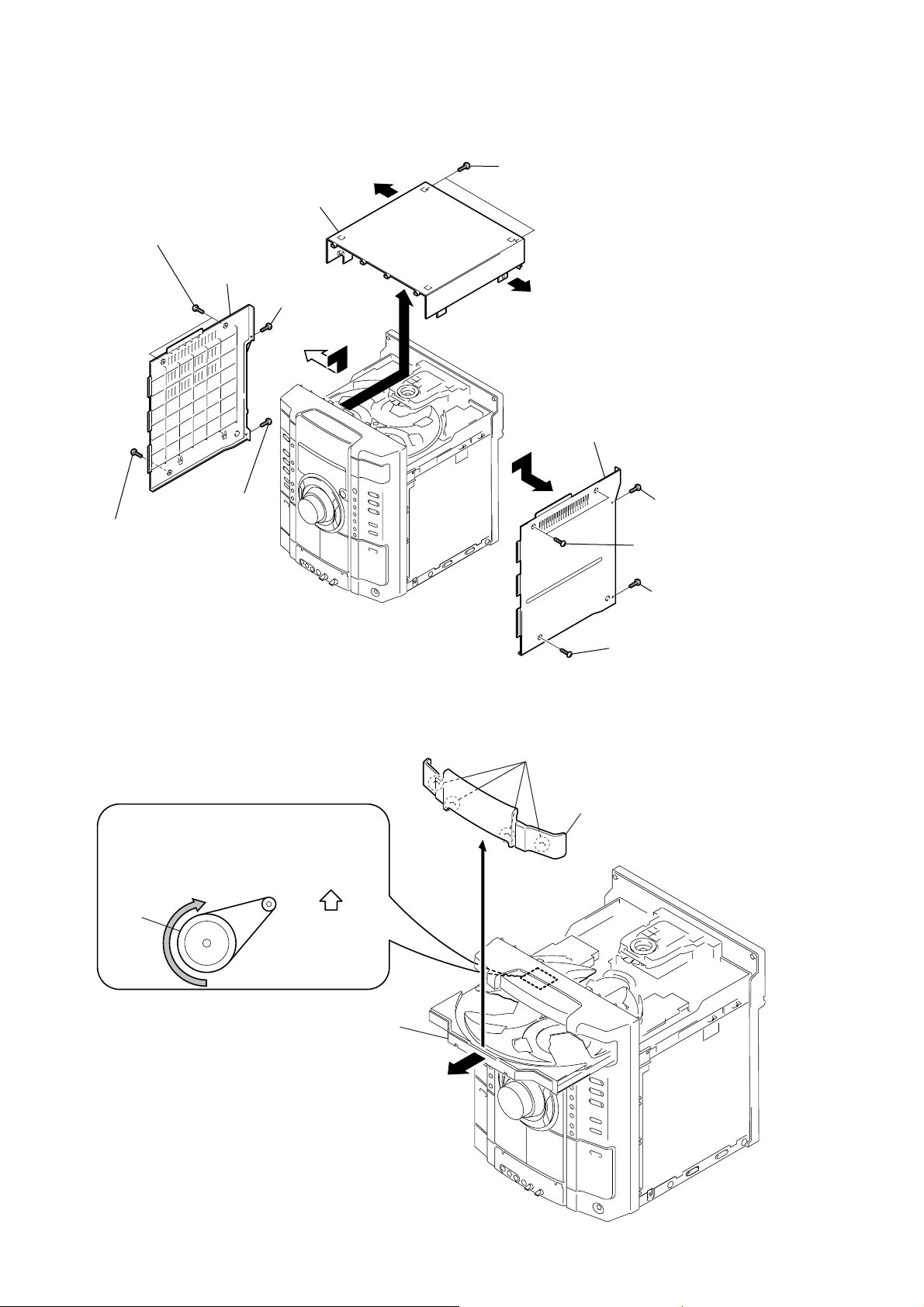
3-3. FRONT PANEL SECTION
qa
qg
CN301 (3P)
1
CN805 (2P)
3
wire (flat type) (11 core)
(CN882)
8
screw
(+BVTP 3
×
10)
4
screw
(+BVTP 3
CN304 (8P)
qf
screw
(+BV 3 (3-CR))
×
8)
5
screw (+BVTP 3
HCD-RV555
×
8)
9
qh
front panel section
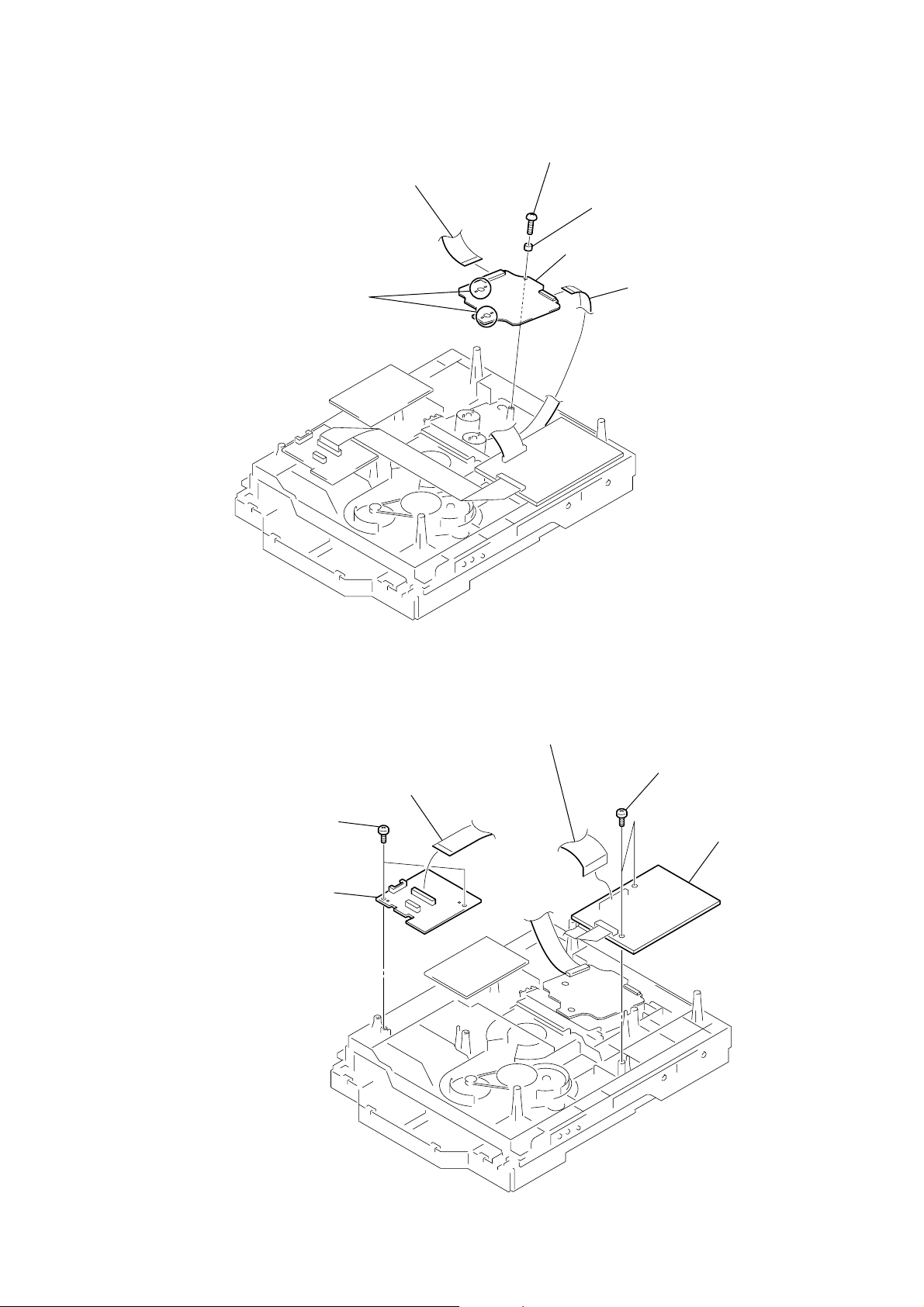
3-4. CD MECHANISM DECK
qd
CN103 (8P)
0
CN309 (5P)
2
wire (flat type) (29 core)
(CN302)
6
three
screws
(+BVTP 3
4
CD mechanism deck
×
qs
CN112 (3P)
7
screw (+BVTP 3
8)
×
10)
1
three
(+BVTP 3
screws
×
10)
MAIN board
MAIN board
3
CN883 (11P)
2
CN701 (12P)
11
Page 12
HCD-RV555
)
)
3-5. TAPE MECHANISM DECK, MICROPHONE JACK BOARD
4
two MIC knobs
1
wire (flat type) (13 core)
jack bracket
3
tape mechanism deck
2
six
screws
(+BVTP 2.6 (3CR)
7
MICROPHONE JACK board
3-6. PANEL BOARD
4
seven
claws
6
two
screws
(+BVTP 2.6 (3CR))
6
CN604 (6P)
5
two
screws
(+BVTP 2.6 (3CR))
2
eight
screws
(+BVTP 2.6 (3CR)
12
5
7
PANEL board
CN605 (5P)
1
wire (flat type) (13 core)
3
two
screws
(+BVTP 2.6 (3CR))
Page 13
3-7. BACK PANEL SECTION, SUB TRANSFORMER BOARD
)
qa
SUB TRANSFORMER board
3
CN901 (2P)
0
two
screws
×
10)
9
5
CN308 (3P)
CN906 (3P)
2
1
CN904 (4P)
(+BVTP 3
qs
back panel section
7
two
(+BVTP 3
8
6
HCD-RV555
screws
×
screw
(+BVTP 3
two
(+BVTP 3
×
screws
×
10)
10)
10
3-8. TRANSFORMER BOARD
6
TRANSFORMER board
1
CN905 (5P)
4
wire (flat type) (11 core)
(CN101)
5
four
(screw)
3
(+BV 3 (3-CR))
screws
screw
2
4
earth wire
CN907 (10P)
13
Page 14
HCD-RV555
d
3-9. MAIN BOARD
1
CN907 (10P)
4
MAIN boar
MAIN board
3-10. AMP BOARD
4
screw
(+BV 3 (3
6
two
(transistor)
8
AMP
screws
board
-
CR))
3
screw
(+BVTP 3
×
14)
3
2
two
(+BVTP 3
CN441
screws
5
×
8)
2
two
screws
×
(+BVTT 4
7
heat sink
8)
14
1
CN905 (5P)
Page 15
3-11. BD BOARD
)
5
Remove the four solders.
1
wire (flat type) (29 core)
(CN101)
3
screw
(+BVTP 2.6
6
BD
4
gap tube
board
× 8
)
2
wire (flat type) (16 core
(CN102)
HCD-RV555
3-12. VCD CONNECT BOARD, VMP BOARD
1
wire (flat type) (19 core)
(CN881)
2
two
screws
(+BVTP 2.6 (3CR))
3
VCD CONNECT
board
4
wire (flat type) (29 core)
(CN101)
5
two
(+BVTP 2.6
screws
6
(3CR)
VMP
)
board
15
Page 16
HCD-RV555
3-13. DRIVER BOARD, SW BOARD
1
two
(+BTTP (M2.6))
4
DRIVER
2
wire (flat type) (5 core)
(CN702)
screws
board
3
CN703 (4P)
5
screw
(+BTTP (M2.6))
6
SW board
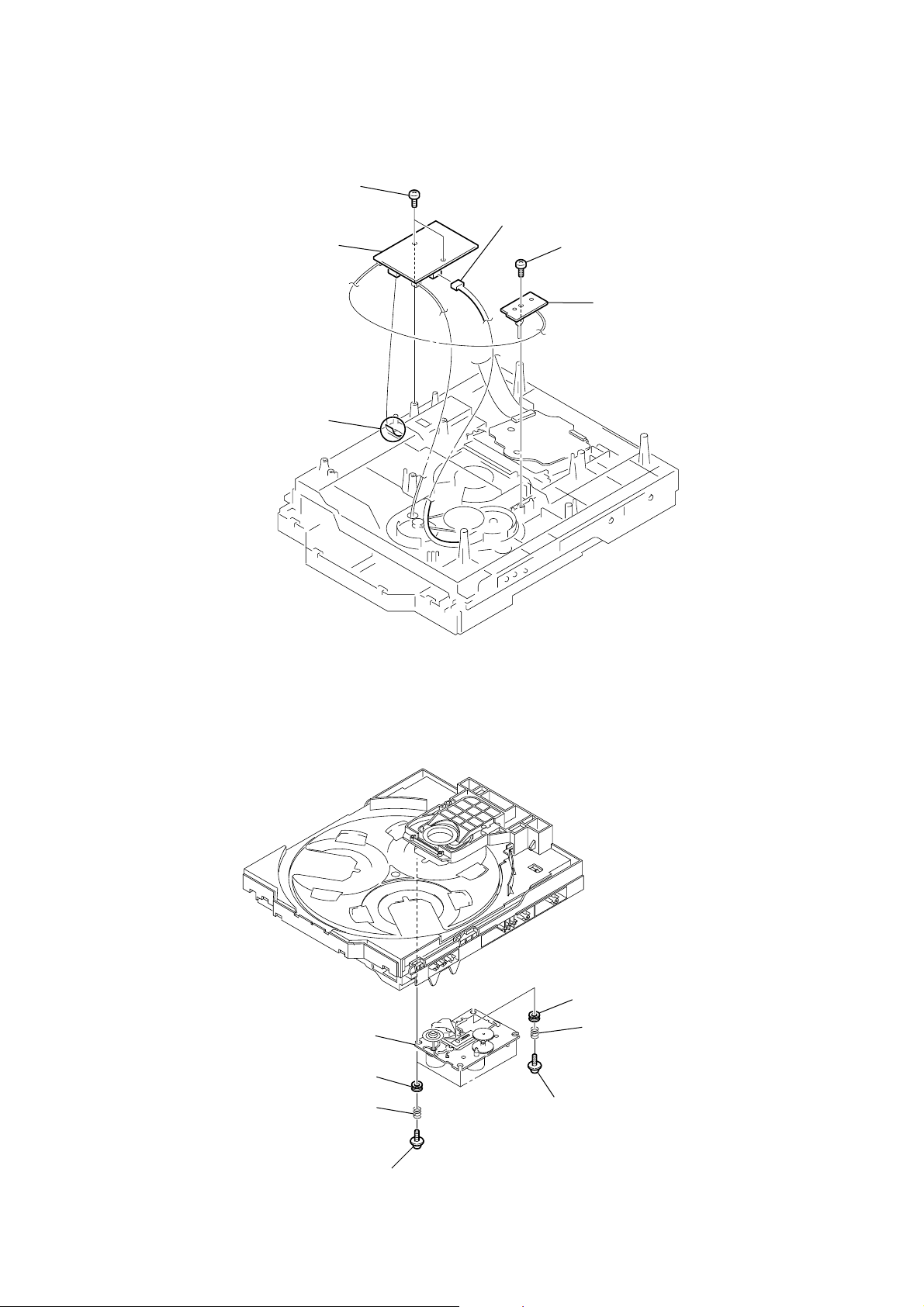
3-14. BASE UNIT
7
base unit
(BU-K4BD49)
6
three
insulators
5
three
(insulator)
coil springs
3
insulator
2
coil spring
(insulator)
1
floating
(+PTPWH M2.6)
screw
16
4
three floating
(+PTPWH M2.6)
screws
Page 17
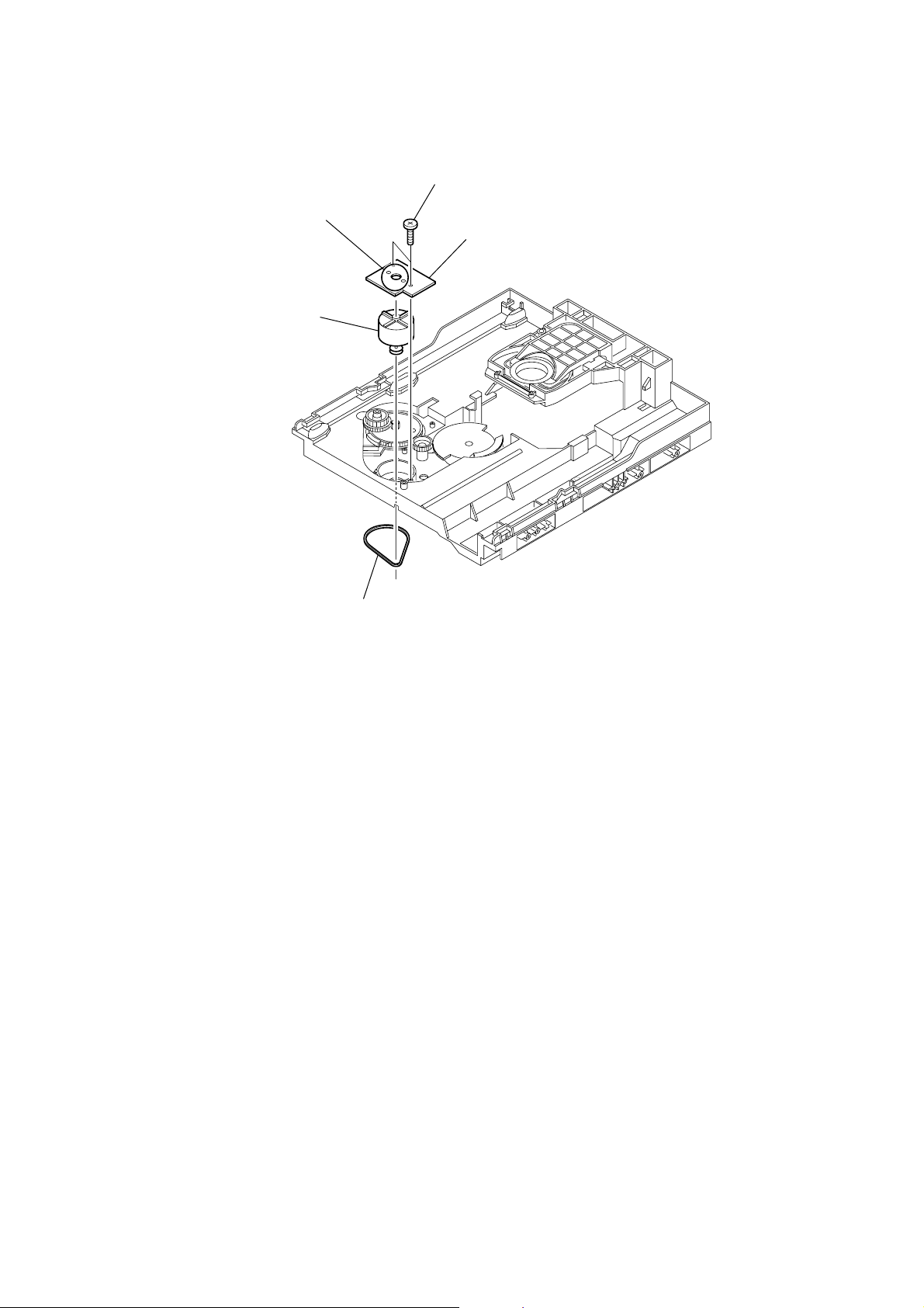
3-15. SENSOR BOARD
2
t
ray
1
floating
(+PTPWH M2.6)
6
floating
(+PTPWH M2.6)
7
g
screw
8
(+BTTP (M2.6))
screw
ear (geneva)
s
crew
0
SENSOR board
9
CN731 (3P)
3
b
elt (table)
4
floating
(+PTPWH M2.6)
5
screw
p
ulley (table)
HCD-RV555
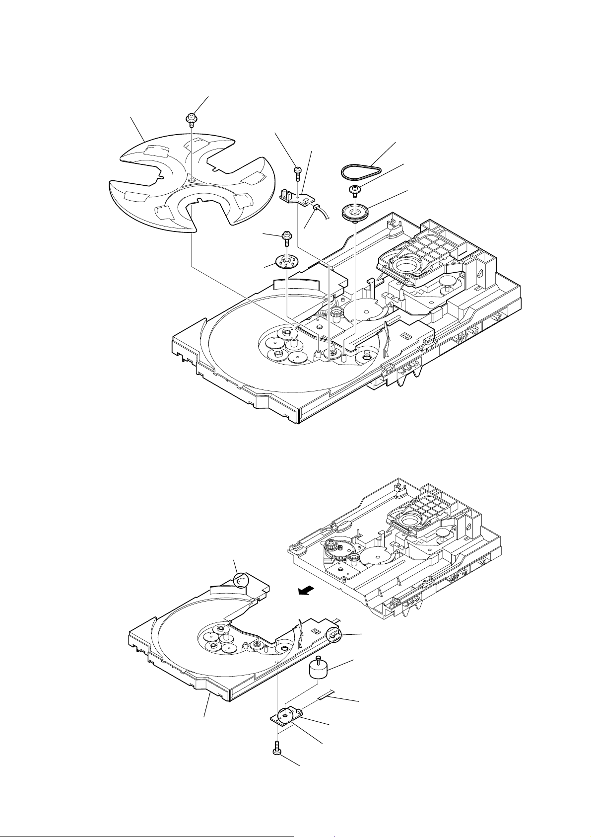
3-16. MOTOR (TB) BOARD
table assy
2
stopper
4
stopper
1
7
t
able motor assy (M741)
3
wire (flat type) (5 core)
(CN742)
8
MOTOR (TB) board
6
Remove the two solders of motor.
5
two
screws
(+BTTP (M2.6))
17
Page 18
HCD-RV555
3-17. MOTOR (LD) BOARD
4
Remove the two solders of motor.
5
l
oading motor assy (M751)
2
two
screws
(+BTTP (M2.6))
3
MOTOR (LD) board
1
b
elt (loading)
18
Page 19

SECTION 4
TEST MODE
HCD-RV555
MC COLD RESET
The cold reset clears all data including preset data stored in the
RAM to initial conditions. Execute this mode when returning the
set to the customer.
Procedure:
1. Press the I/1 button to turn the power ON.
2. Press three buttons of x , [PLAY MODE/TUNING MODE] and
[DISC 1] simultaneously.
3. The message “COLD RESET” is displayed on the fluorescent
indicator tube momentarily, then becomes standby states.
AM TUNING INTERVAL CHANGE-OVER
A step of AM tuning interval can be changed over between 9 kHz
and 10 kHz.
Procedure:
1. Press the I/1 button to turn the power on.
2. Press the [TUNER/BAND] button to select “AM”.
3. Press the I/1 button to turn the power off.
4. Press two buttons of [PLAY MODE/TUNING MODE] and I/1
simultaneously.
5. The message “AM 9K STEP” or “AM 10K STEP” is displayed
on the fluorescent indicator tube, and thus the channel step is
changed over.
CD SHIP (LOCK) MODE
This mode moves the optical pick-up to the position durable to
vibration. Use this mode when returning the set to the customer
after repair.
Procedure:
1. Press the I/1 button to turn the power on.
2. Press the [CD] button to select “CD”.
3. Press two buttons of [CD] and I/1 simultaneously.
4. The message “LOCK” is displayed on the fluorescent indicator
tube, and the CD ship mode is set.
CD SHIP (LOCK) MODE & COLD RESET
This mode is used to perform CD chip (lock) mode and cold reset
simultaneously.
Procedure:
1. Press the I/1 button to turn the power on.
2. Press the [CD] button to select “CD”.
3. Press three buttons of x , [CD] and I/1 simultaneously.
4. The message “COLD RESET” is displayed on the fluorescent
indicator tube momentarily, then becomes standby states.
CHANGE-OVER FUNCTION OF SAT/VIDEO
This mode is used to enable function of external input to change
over between SAT and VIDEO.
Procedure:
1. Press the I/1 button to turn the power on.
2. Press two buttons of VIDEO/SAT and I/1 simultaneously.
3. The message “SAT” or “VIDEO” is displayed on the
fluorescent indicator tube, and the function of external input
is changed over.
CD TRAY LOCK MODE
This mode is used to unable to take sample disc out of tray in the
shop.
Procedure:
1. Press the
2. Press the [CD] button to select “CD”.
3. Set disc on the CD tray, press two buttons of
seconds.
4. The message “LOCKED” is displayed on the fluorescent
indicator tube and the CD tray is locked. (Even if pressing
the Z button, the message “LOCKED” is displayed on the
fluorescent indicator tube and the CD tray is locked)
5. To release from this mode, press two buttons of x and Z for
5 seconds.
6. The message “UNLOCKED” is displayed on the fluorescent
indicator tube and the CD tray is unlocked.
I/1 button to turn the power on.
x and Z for 5
AMP TEST MODE
This mode is used to display the parameter of amplifier IC and
display the VACS status.
Procedure:
1. Press the I/1 button to turn the power on.
2. Press three buttons of x , [PRESET EQ] and [PLAY MODE/
TUNING MODE] simultaneously.
3. When the AMP test mode is activated, the message “AMP
TEST IN” is displayed on the fluorescent indicator tube
momentarily, then amplifier adjustment mode is displayed on
the fluorescent indicator tube.
4. Press the [DISPLAY] button to changed over between VACS
status display mode and the amplifier IC parameter display
mode.
5. In the amplifier IC parameter display mode, press the
[GROOVE] button to changed over DBFB on/off, and when it
is on, the character “D” is displayed on the fluorescent indicator
tube.
6. In the amplifier IC parameter display mode, press the
[SURROUND] button to changed over surround on/off, and
when it is on, the character “S” is displayed on the fluorescent
indicator tube.
7. In the amplifier IC parameter display mode, turn each knob of
. >
[ -- EQ + ] causes respective parameters to be changed,
as well as change-over of the display on the fluorescent
indicator tube.
CD SERVICE MODE
This mode can run the CD sled motor freely. Use this mode, for
instance, when cleaning the optical pick-up.
Procedure:
1. Press the I/1 button to turn the power on.
2. Press the [CD] button to select “CD”.
3. Press three buttons of x , [PLAY MODE/TUNING MODE] and
Z simultaneously.
4. When the CD service mode is activated, the message “MPEG
AV TEST” is displayed on the fluorescent indicator tube.
5. Press the M/ALBUM + button, optical pick-up move to outside
track and the message “SLED OUT” is displayed on the
fluorescent indicator tube.
6. Press the m/ALBUM – button, optical pick-up move to inside
track and the message “SLED IN” is displayed on the
fluorescent indicator tube.
7. Press the [ENTER] button, traverse on/off is changed over.
8. Press the [EQ BAND] button when MPEG AV Test mode is
activated, the massage “SERVICE MODE” is displayed on
the fluorescent indicator tube and AV Test mode is activated.
19
Page 20
HCD-RV555
AGING MODE
This mode can be used for operation check of CD section and tape
deck section.
CD section and tape deck section work in parallel.
If an error occurred:
The aging operation stops only an error occurred sections and display
then status.
If no error occurs:
The aging operation continues repeatedly.
Procedure:
1. Press the I/1 button to turn the power on.
2. Press the [CD] button to select “CD”.
3. Set disc on the CD tray and set tape into the deck.
4. Press three buttons of x , [PLAY MODE/TUNING MODE] and
[DISC SKIP/EX-CHANGE] simultaneously.
5. Aging operations of CD and tape are started at the same time.
6. To release from this mode, press the I/1 button to turn the
power off and press the function buttons.
1. Display at the Aging Mode
Display operating state of CD section and tape deck section
alternately.
If an error occurred, stop display which that section.
2. CD Section
The sequence during the aging mode is following as below.
Display at the aging mode is the same as the normal operation.
Aging mode sequence (CD section) :
3. Tape Deck Section
The sequence during the aging mode is following as below.
If an error occurred, stop display that step.
Aging mode sequence (tape deck section) :
Rewind the tape A and B
“TAPE AAG-1 or TAPE BAG-2”
Shut off
FWD play the tape A
“TAPE AAG-3”
2 minutes
Rewind the tape A
“TAPE AAG-6”
Shut off
FWD play the tape B
“TAPE BAG-3”
2 minutes
Rewind the tape B
“TAPE BAG-6”
Shut off
Start (from disc 1)
Disc chucking
TOC read
Play first track for 2 seconds
Play last track for 2 seconds
EX-change open/close
Open the disc tray
Disc skip
Close the tray
Change the next disc.
Note: “TAPE *AG-*” is display of each step.
PANEL TEST MODE
This mode is used to check the fluorescent indicator tube, LEDs
and buttons.
Procedure:
1. Press the I/1 button to turn the power on.
2. Press three buttons of x , [PLAY MODE/TUNING MODE] and
[ENTER] simultaneously.
3. Fluorescent indicator tube and LEDs are all turned on.
4. Press two buttons of X and [ENTER] simultaneously, mode
is changed over.
5. In the key check mode, press each key, the defined key number
of every each key list is displayed on the fluorescent indicator
tube.
6. In the key count check mode, “KEYCNT 0” is displayed on
the fluorescent indicator tube. Each time a key is pressed, “K”
value increases. However, once a key is pressed, it is no longer
taken into account.
7. In the headphone input check mode, connect the headphone,
the message “H_P ON” is displayed on the fluorescent
indicator tube, and disconnect the headphone, the message
“H_P OFF” is displayed on the fluorescent indicator tube.
8. In the volume check mode, “VOLUME FLAT” is displayed
on the fluorescent indicator tube. Turn the [VOLUME] knob
clockwise, the message “VOLUME UP” is displayed on the
fluorescent indicator tube momentarily and turn the [VOLUME]
knob counterclockwise, the message “VOLUME DOWN” is
displayed on the fluorescent indicator tube momentarily.
20
Page 21
HCD-RV555
MC TEST MODE
This mode is used to check operations of microprocessor.
Procedure:
1. Press the I/1 button to turn the power on.
2. Press three buttons of
x , [PLAY MODE/TUNING MODE] and
[DISC 3] simultaneously.
3. When the MC test mode is activated, VACS level is displayed
on the fluorescent indicator tube momentarily.
4. Turn the [ -- EQ + ] knob clockwise, the message “ALL
. >
EQ MAX” is displayed on the fluorescent indicator tube
momentarily and turn the [ -- EQ + ] knob counterclock-
. >
wise, the message “ALL EQ MIN” is displayed on the
fluorescent indicator tube momentarily.
5. Press the [PRESET EQ] button, the message “ALL EQ FLAT”
is displayed on the fluorescent indicator tube momentarily.
6. Turn the [VOLUME] knob clockwise, the message “VOLUME
MAX” is displayed on the fluorescent indicator tube
momentarily and turn the [VOLUME] knob counterclockwise,
the message “VOLUME MIN” is displayed on the fluorescent
indicator tube momentarily.
7. Press the [GROOVE] button to changed over VACS on/off.
8. When the [REC PAUSE/START] button is pressed twice with a
tape set in the deck-B, the function is switched “MD” or
“VIDEO” and recording starts. When the
M/ALBUM + button is pressed during recording, the tape is
m/ALBUM – or
rewound back to the beginning of recording, the function is
switched to “TAPE B”, then playback starts.
9. When the [CD SYNC] key is pressed with the test tape (AMS-
100, AMS-110A) in the deck, number of space between tunes
is counted, then if AMS-110A is set, “OK” is displayed on the
fluorescent indicator tube and if AMS-100 is set, “NG” is
displayed on the fluorescent indicator tube.
10. Press the
I/1 button to release from this mode, then cold reset
is performed.
VERSION DISPLAY MODE
This mode is used to check the model, destination and software
version.
Procedure:
1. Press the I/1 button to turn the power on.
2. Press three buttons of x , [PLAY MODE/TUNING MODE] and
[DISC 2] simultaneously.
3. When this mode is activated, model and destination is
displayed on the fluorescent indicator tube.
4. Press the [DISPLAY] button to changed over between software
version and year, month, day of the software creation display
mode and model and destination display mode.
5. To release from this mode, press three buttons of x , [PLAY
MODE/TUNING MODE] and [DISC 2] simultaneously.
CD ERROR CODE DISPLAY MODE
This mode can be used for error code display of CD section.
Procedure:
1. Press the I/1 button to turn the power on.
2. Press the [CD] key to select “CD”.
3. Press three buttons of x , [CD] and [DISC 1] simultaneously.
4. When this mode is activated, mechanism deck error code is
displayed on the fluorescent indicator tube.
5. Press the [GROOVE] button to changed over between optical
pick-up error code display mode and mechanism deck error
code mode.
6. Turn the [ -- EQ + ] knob to change over display of error
history.
. >
1. Mechanism Deck Error Code Mode
When this mode is entered, mechanism deck error code is displayed
with the 10-character format on the fluorescent indicator tube.
The first digit from the left indicates:
The first digit from the left indicates which mode the error history
is. In the mechanism deck error code mode, “M” is displayed on
the fluorescent indicator tube.
The second digit from the left indicates:
(Error history No. display)
The second digit from the left indicates which order the error history
is. “1” indicates the latest error history, and each time the number
increases by one, the error history goes back to one-previous error.
The third and 4th digit from the left indicates:
(Error status display)
The third and 4th digit from the left indicates which error status is
indicated.
Display Status
00 No error
08 Tab le operation time-out (Table does not move to the target
position within the specified time)
16 In the chucking down operation, the operation was retried
by the maximum number of times but the operation could
not be completed
17 In the chucking up and down operation, the reverse
recovery processing was attempted but it could not be
recovered
18 In the chucking up operation, the operation was retried by
the maximum number of times but the operation could not
be completed
20 Loading operation time-out (Table does not move to the
target position within the specified time)
22 As the chuck was in the ex-open status at the initialization,
the closing was attempted but could not be completed
The 5th and 6th digit from the left indicates:
(Present status display)
The 5th and 6th digit from the left indicates which operating status
when an error occurred is indicated.
Display Status
01 Open completion status
02 From open status, the movement to chucking down position
is under way
03 From chucking down position, the open operation is under
way
04 Chucking down completion status
10 The chucking down operation is under way
11 The chucking up operation is under way
12 Close completion status
13 From close status, the ex-open operation is under way
14 From ex-open status, the close operation is under way
18 Ex-pen completion status
21
Page 22
HCD-RV555
The 7th and 8th digit from the left indicates:
(Motor status display)
The 7th and 8th digit from the left indicates which motor output
status when an error occurred is indicated.
Display Status
× 0 No table motor output
× 1Table motor forward output
× 2Table motor backward output
× 3Table motor break output
0 × No loading motor output
1 × Loading motor forward output
2 × Loading motor backward output
3 × Loading motor break output
The 9th and 10th digit from the left indicates:
(Tray status display)
The 9th and 10th digit from the left indicates which target processing
when an error occurred is indicated.
Display Status
01 Open operation
12 Close operation
18 Ex-open operation
2. Optical Pick-up Error Code Mode
When this mode is entered, optical pick-up error code is displayed
with the 8-character format on the fluorescent indicator tube.
The first digit from the left indicates:
The first digit from the left indicates which mode the error history
is. In the optical pick-up error code mode, “D” is displayed on the
fluorescent indicator tube.
The second digit from the left indicates:
(Error history No. display)
The second digit from the left indicates which order the error history
is. “1” indicates the latest error history, and each time the number
increases by one, the error history goes back to one-previous error.
The third and 4th digit from the left indicates:
(Error status display)
The third and 4th digit from the left indicates which error status is
indicated.
Display Status
01 Not focused (TOC read without a disc)
02 GFS NG (TOC read with a disc chucked)
03 Start operation time-over
04 Defocused continuously (Defocused during TOC reading)
05 Q code not entered for specified time
06 Tracking not turned ON
07 Blank disc (Blank disc TOC read)
The 5th and 6th digit from the left indicates:
(Error step display)
The 5th and 6th digit from the left indicates which processing when
a trouble occurred
Display Contents
01 Power OFF in progress
02 Initialize in progress
03 Oscillation stopping
04 From oscillation stop, oscillation starting
05 Stopping
06 Stop operation is under way
07 Start operation in progress
08 TOC read in progress
09 Search operation is under way
0A Playback operation is under way
0B Pause operation is under way
0C Playback manual search operation is under way
0D Pause manual search operation is under way
0E —
The 7th and 8th digit from the left indicates:
The 7th and 8th digit from the left indicates which operation in
progress when a trouble occurred. (Step of each processing of the
5th and 6th digits is indicated)
5 REPEAT LIMIT CANCEL MODE
Number of repeat for CD playback is 5 times when the repeat mode
is “REPEAT”. This mode is used to enables CD to repeat playback
for limitless times.
Procedure:
1. Press the
I/1 button to turn the power on.
2. Press the [CD] button to select “CD”.
3. Press three buttons of x , [CD] and [ENTER] simultaneously.
4. The message “LIMIT OFF” is displayed on the fluorescent
indicator tube momentarily, CD repeat 5 limit is cancelled.
VCD COLOR SYSTEM MODE
This mode is used to change over color system.
Procedure:
1. Set to the standby state.
2. Press two buttons of m/ALBUM – and I/1 simultaneously
to change the color system to PAL, and the message “COLOR
PA L” is displayed on the fluorescent indicator tube.
3. Press two buttons of X and I/1 simultaneously to change
the color system to AUTO, and the message “COLOR AUTO”
is displayed on the fluorescent indicator tube.
4. Press two buttons of M/ALBUM + and I/1 simultaneously
to change the color system to NTSC, and the message
“COLOR NTSC” is displayed on the fluorescent indicator
tube.
22
Page 23
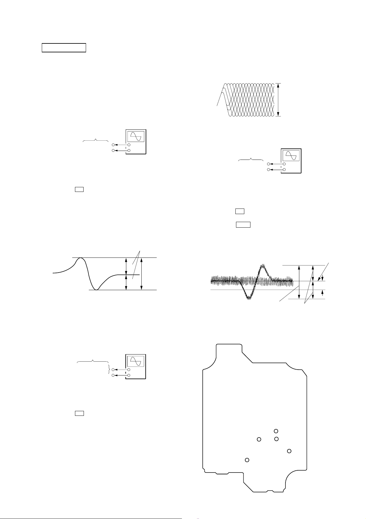
SECTION 5
)
TP2 (TE)
TP10 (VC)
BD board
+
–
oscilloscope
RF signal waveform
VOLT/DIV : 200mV
TIME/DIV : 500ns
level : 0.75
±
0.1Vp-p (RFDC)
1.05
±
0.3Vp-p (RFAC)
p
ELECTRICAL ADJUSTMENTS
HCD-RV555
CD SECTION
Note:
1. CD Block is basically designed to operate without adjustment.
Therefore, check each item in order given.
2. Use LUV-P01 (Part No. 4-999-032-01) unless otherwise indicated.
3. Use an oscilloscope with more than 10 MW impedance.
4. Clean the object lens by an applicator with neutral detergent when the
signal level is low than specified value with the following checks.
S-CURVE CHECK
oscilloscope
BD board
TP4 (FE)
TP10 (VC)
Procedure:
1. Connect an oscilloscope to TP4 (FE) and TP10 (VC) on the
BD board.
2. Press the I/1 button to turn the power on.
3. Load the disc (LUV-P01) and actuate the focus search. (In
consequence of open and close the disc tray, actuate the focus
search)
4. Confirm that the oscilloscope waveform (S-curve) is
symmetrical between A and B. And confirm peak to peak level
within 2 ± 0.5 Vp-p.
S-curve waveform
+
–
symmetry
A
within 2
B
±
0.5Vp-
Note: Clear RF signal waveform means that the shape “ ◊ ” can be clearly
distinguished at the center of the waveform.
TRAVERSE LEVEL CHECK
Procedure:
1. Connect an oscilloscope to TP2 (TE) and TP10 (VC) on the
BD board.
2. Press the I/1 button to turn the power on.
3. Load the disc (LUV-P01) and playback the number nine track.
4. Press the hH button. (Becomes the 1 track jump mode.)
5. Confirm that the level B and A (DC voltage) on the oscilloscope
waveform.
1 track jump waveform
B
VC
center of
waveform
A (DC voltage
Note: • Try to measure several times to make sure than the ratio
of A : B or B : A is more than 10 : 7.
• Ta ke sweep time as long as possible and light up the
brightness to obtain best waveform.
RF LEVEL CHECK
BD board
TP6 (RFDC)
TP5 (RFAC)
TP10 (VC)
Procedure:
1. Connect an oscilloscope CH1 to TP6 (RFDC), CH2 to TP5
(RFAC) and TP10 (VC) on the BD board.
2. Press the I/1 button to turn the power on.
3. Load the disc (LUV-P01) and playback the number nine track.
4. Confirm that oscilloscope waveform is clear and check if RF
signal level is correct or not.
oscilloscope
+
–
level=1.2 ±0.55Vp-p
Connecting Location:
– BD BOARD (SIDE B) –
TP6
(RFDC)
TP5 (RFAC)
symmetry
TP4 (FE)
TP2 (TE)
TP10 (VC)
23
Page 24
HCD-RV555
r
r
VIDEO SECTION
AUDIO LEVEL, VIDEO CLOCK, AUDIO SERVO
CLOCK CHECK
VMP board
TP415 (L-OUT)
TP413 (R-OUT)
VMP board
TP70 (54 MHz)
TP182 (4.2336 MHz)
Procedure:
1. Connect an oscilloscope to TP308 (V-OUT) on the VMP
board.
2. Connect a level meter to TP415 (L-OUT) and TP413 (R-OUT)
on the VMP board.
3. Connect a frequency counter to TP70 (54 MHz) and TP182
(4.2336 MHz) on the VMP board.
4. Press the I/1 button to turn the power on.
5. Set a test disc (HLV-402 (Part No. 8-909-870-00))
6. Set to the MPEG AV TEST mode. (Refer to the CD SERVICE
MODE (See page 19))
7. The message “MPEG AV” is displayed on the fluorescent
indicator tube. Color bar signal outputs and sine-wave (1 kHz
0 dB) appears.
8. Confirm that the value of level meter is 2.5 ± 2.0 dBs. (If
audio output disappear, press the [PRESET EQ] button, and
the message “SERVICE MODE” is displayed on the
fluorescent indicator tube)
9. Confirm that the value of frequency counter is 54 MHz ± 400
Hz.
10. Confirm that the value of frequency counter is 4,2336 MHz.
11. Change disc to a MP3 test disc (MP3 1 kHz 0 dB sine-wave is
recorded)
12. Confirm that the value of level meter is 2.4 ± 2.0 dBs.
level mete
+
–
frequency counte
+
–
– VMP BOARD (SIDE A) –
TP70
(54 MHz)
TP182
(4.2336 MHz)
TP415
(L-OUT)
TP413
(R-OUT)
24
Page 25
SECTION 6
DIAGRAMS
6-1. BLOCK DIAGRAM — CD SERVO SECTION —
FOCUS/TRACKING ERROR AMP
DETECTOR
OPTICAL PICK-UP
BLOCK
LASER DIODE
PD
M102
M
(SPINDLE)
M101
M
(SLED)
2-AXIS
DEVICE
(TRACKING)
(FOCUS)
A
B
C
D
E
F
LD
LD
PD
SP+
SP-
SD+
SD-
T+
T-
F+
F-
6
7
8
9
11
10
AUTOMATIC
POWER
CONTROL
Q101
A
B
C
D
F
E
16
15
14
13
12
11
18
17
F I-V AMP
E I-V AMP
LD
1
SP+
SP–
SD+
SD–
TD+
TD–
FD+
FD–
RF
SUMMING
AMP
FOCUS
ERROR AMP
RF DC
AMP
TRACKING
ERROR AMP
APC LD
AMP
FOCUS/TRACKING COIL DRIVE,
SPINDLE/SLED MOTOR DRIVE
IC150
MOTOR
DRIVE
MOTOR
DRIVE
COIL
DRIVE
COIL
DRIVE
SFDR
SRDR
TFDR
TRDR
FFDR
FRDR
MUTE
20
AC
SUM
FEI
RFDCO
RFDCI
TE_BAL
DVC
SW
24
26
4
5
6
7
22
23
RF AMP,
IC103
FE
TE
PD
HCD-RV555
FREQUENCY
SELECT SWITCH
Q102
FILTER
189
MDP
133
24
XTSL
GPIO9
SFDR
SRDR
137 138 140
12
DI
11
CLK
10
LD
171
168 170
FILO
DIGITAL SIGNAL PROCESSOR,
DIGITAL SERVO PROCESSOR
TFDR
TRDR
FFDR
141
142
DATA
CLK
LD
PCO
IC505 (1/2)
FRDR
143
169
CLTV
81
FILI
SYSRST
IC701
IC712
INV.
Q731
ROTARY
ENCODER
RE701
TO IC505 (2/2)
AUDIO/VIDEO
SECTION
LM-F
7FIN
LM-R
9RIN
TM-F
7FIN
TM-R
9RIN
TABLE
E-3
E-2
E-1
O/C
91
PCMD
93
BCK
88
LRCK
124
C2PO
102
DATA
111
CLOK
109
XLAT
113
SENS
126
SCOR
96
SQSO
98
L SQCK
114
L SCLK
121
GFS
131
L FOK
105
L CDXRST
SSTP
135
When the optical
ON :
S101
(LIMIT)
pick-up is inner
position
M751
(LOADING)
M741
(TABLE)
L CDDATA
90
92
L CDBCK
87
L CDLRCK
123
L CDC2PO
103
L DDAT
110
L DCLK
108
L XLAT
112
L SENS
125
L SCOR
95
L SQSO
99
SQCK
115
SCLK
120
L GFS
132
FOK
106
XRST
M
M
TABLE
SENSOR
IC731
DISC TRAY
ADDRESS DETECT
S751
(OPEN)
LOADING MOTOR DRIVE
4 OUT1
2 OUT2
TABLE MOTOR DRIVE
4 OUT1
2 OUT2
OPEN
CLOSE
26
EQ
IN
4
16
17
28
29
18
19
14
12
2
27
3
RFAC
LD ON (D/A4)
2
VCA
D/A1
D/A3
FEBAL
D/A2
RFC
RFAC
EQ
D/A1
D/A2
D/A3
LD ON (D/A4)
FEBAL
15
173
RFAC
164
FE
160
RFDC
162
TE
163
SE
161
CE
165
VC
D/A
CONVERTER
IC506
3
AO3
5
AO4
AO5
6
9
AO6
2
AO2
RST
4
• SIGNAL PATH
: CD PLAY
LM-F
LM-R
TM-F
TM-R
TABLE
TRAY
O/C
DATA
CLK
LD
SYS RST
MAIN
A
SECTION
(Page 27)
AUDIO/VIDEO
B
(Page 26)
AUDIO/VIDEO
C
(Page 26)
AUDIO/VIDEO
D
(Page 26)
CD
SECTION
CD
SECTION
CD
SECTION
HCD-RV555
25 25
Page 26
HCD-RV555
6-2. BLOCK DIAGRAM — AUDIO/VIDEO CD SECTION —
NVOEL
74
24
OE
D0 – D7
13 – 15, 17 – 21
DQ0 – DQ7
XTAO
150 149
X501
33.8688MHz
12 – 5, 27, 26, 31
A0 – A9, A18
PROGRAM ROM
IC508
XTAI
A0 – A10
CLKB
207 206
X502
27MHz
CLKA
D11, D12, D15
28, 29, 30
A13, A14, A17
ADDRESS BUS
DATA BUS
MPEG VIDEO/AUDIO DECODER,
VIDEO SIGNAL ENCODER
DRDAT0 – DRDAT15
D0 – D15
2, 4, 5, 7, 8, 10, 11, 13, 42,
44, 45, 47, 48, 50, 51, 53
DQ0 – DQ15
IC505 (2/2)
DRADR0 – DRADR10
34 – 37, 39 – 4549 – 56, 59 – 66
D0 – D15
A0 – A10
23 – 26, 29 – 34, 22
A0 – A10
A0 – A10
D-RAM
IC507
FROM IC505 (1/2)
DRCAS
DRRAS
DRCK
DRWEL
73 72 68
70 76 77 78
18
16 17 20
38 15
WE
CLK
CAS
RAS
CD SERVO
SECTION
DRDQM0
DRBS
39
BA0
LDQM
DRDQM1
UDQM
GPIO1
GPIO0
13 14
99
98
I-SYS-IN
O-SYS-OUT
GPIO5
GPIO2
15 19 18 16
96
95
100
0-CD-DATA
O-MP3-CLK
O-VIDEO-MUTE
AUDDTO0
AUDBCK
AUDLRCK
AUDXCLKO
GPIO3
GPIO4
97
I-SENS
O-CD-CLK
GPIO14
GPIO13
GPIO11
GPIO12
CPSIG
+3.3V
REGULATOR
Q581
5
VDD
201
203
204
205
30
29
26
28
6
DATA
2
1
BCK
3
LRCK
16
MLCK
DATA
13
14
CLK
15
LAT
DIGITAL FILTER,
D/A CONVERTER
IC504
6
VOUTL
VOUTR
VCC
CD +5V
7
8
LOW-PASS
FILER
IC102
R-CH
MUTING
Q306
MUTE
CONTROL
Q304, 305
R-CH
CD L
CD MUTING
MAIN
E
SECTION
(Page 27)
MAIN
F
SECTION
(Page 27)
LD
CLK
DATA
DATA
CLK
LD
VIDEO AMP
IC307
B.P.F.
7
SYNC BUFFER
Q301
3
CONTROL SWITCH
OUT
IN
OUTSAG
STBY
2
VIDEO MUTING
Q370
6
5
VIDEO SELECTOR
IC803
1
3
2
7
J805 (1/2)
VIDEO SW
J803
VIDEO
OUT
VIDEO
CD SERVO
C
SECTION
(Page 25)
GAME
INPUT
PANEL/POWER
G
(Page 28)
SECTION
HCD-RV555
• R-ch is omitted due to same as L-ch.
• SIGNAL PATH
: CD PLAY (AUDIO)
: CD PLAY (VIDEO)
: MIC
CD SERVO
SECTION
(Page 25)
CD SERVO
SECTION
(Page 25)
SYSTEM CONTROLLER
IC601 (1/3)
JK802
MIC
MIC +10V
MIC AMP
IC801 (1/2)
VR801
MIC LEVEL
MIC AMP
IC801 (2/2)
MIC
H
MAIN
SECTION
(Page 27)
TABLE
B
TRAY
O/C
SYS RST
D
TABLE
TRAY
O/C
73 I-CD NUM SENSOR
20 I-CD ENCODER
21 I-CD OPEN/CLOSE
93 O-XRES (RESET)
WFR/HP/MIC-IN
MUTING
Q802
MIC DETECT
Q372
19
+
MIC AGC
Q801
ECHO AMP
IC802
VR802
ECHO LEVEL
HP CTL
MAIN
I
SECTION
(Page 27)
2626
Page 27

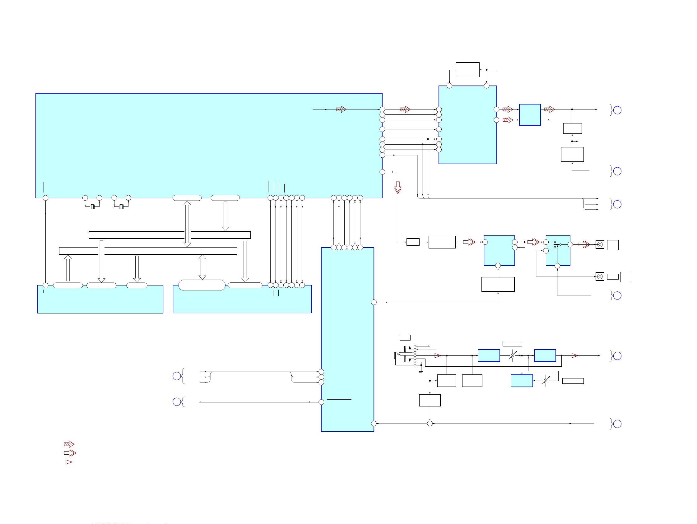
6-3. BLOCK DIAGRAM — MAIN SECTION —
FM 75Ω
COAXIAL
AM
AUDIO/VIDEO
CD SECTION
(Page 26)
AUDIO/VIDEO
CD SECTION
(Page 26)
HP901
(PB)
(DECK-A)
MIC
H
JK805 (2/2)
GAIN INPUT
AUDIO
E
FM/AM TUNER PACK
FM ANT
ANT GND
AM ANT
ANT GND
L-CH
R-CH R-CH
L-CH
L
R
CD L
TM901
TUNER-L
TUNER-R
LC72121 DI
LC72121 DO
LC72121 CLK
LC72121 CE
TUNED
STEREO
TU MUTE
R-CH
R-CH
DI
DO
CLK
CE
TUNED
STEREO
TU-MUTING
59
1
61
3
7
9
11
GAME L
CD L
TUNER L
TAPE L
PB OUT1
TAPE A1
TAPE B1
58
MIC
TONE OUT1
ELECTRICAL VOLUME
37
INPUT SELECT,
TONE CONTROL,
IC101
36
LINE OUT1(L)
LINE OUT1(R)
VIN1
MD L
MD R
VOL OUT1
SAOUT2
AMS OUT
REC OUT1
SI
SC
19
18
HCD-RV555
Ver. 1.2
JK101
63
64
54
53
33
55
40
15
R-CH
R-CH
FEED BACK
SWITCH
Q106
D201
R-CH
BIAS
Q105
B+9V
LINE AMP
IC102
R-CH
MUTE
Q103
MUTE
CONTROL
Q101, 102
R-CH
R-CH
POWER
AMP
IC441
STANDBY
SWITCH
Q489
POWER AMP
ON/OFF
Q308, 309, 313
TH441
AC4
THERMAL
DETECT
Q483, 484
OVER LOAD
DETECT
Q441, 442
D481
+
PROTECT
DETECT
Q485, 487
+
DC
DETECT
Q481, 482
–1
–2
RY441
PROTECTOR
Q486, 488
R-CH
R-CH
RY B+
+
JK441
+
–
+
–
+
–
+
–
L
R
L
R
L
R
L
R
IN
OUT
USE 6 – 16Ω
VIDEO/SAT
FRONT
SPEAKER
IMPEDANCE
SURROUND
SPEAKER
IMPEDANCE
USE 6 – 16Ω
J801
PHONES
HRPE901
(REC/PB/ERASE)
(DECK-B)
(Page 26)
AUDIO/VIDEO
CD SECTION
PANEL/
POWER SUPPLY
SECTION
(Page 28)
R-CH R-CH
ERASE
LM-F
CD SERVO
SECTION
(Page 25)
F
J
LM-R
A
TM-F
TM-R
CD MUTING
FRONT SP RELAY
REC/PB
SWITCH
IC201,
Q322, 323
BIAS OSC
L101
TU-MUTING
LM-F
LM-R
TM-F
TM-R
DI
CE
DO
CLK
TUNED
STEREO
83
86
84
67
85
O-LC72121/BU2099FV DO
68
I-TUNED-IN
I-LC72121 DI
I-STEREO-IN
O-LC72121 CE
O-LC72121/BU2099FV CLK
11
14
13
16
15
10
17
BIAS OSC
Q321
Q5
Q8
Q7
Q10
Q9
Q4
Q11
BIAS
SWITCH
Q324
DATA DECODER
7
Q16Q0
DATA4CLOCK5LCH
3
IC371
Q6
12
87
O-BU2099FV LCH
B +9V
91
88
O-BD3401 CLK
O-BD3401 DATA
AMS DETECT
Q327
69
I-AMS-IN
SYSTEM CONTROLLER
Q351, 352
IC601 (2/3)
AMP
D604
24
I-STREAM/VACS
18
I-PROTECT
75
O-SYSTEM-MUTE
4
2
O-MP3 LP
I-MP3 REQ
3
I-TAPE A STAT
O-MP3 ACK
I-TAPE B STAT
I-REEL A IN
I-REEL B IN
Q606
Q608
Q607
22
23
70
71
CAPSTAN/REEL
MOTOR DRIVE
Q601
PLUNGER DRIVE
Q603
PLUNGER DRIVE
Q602
D207
+
TAPE MECHANISM
DECK BLOCK
MM
(CAPSTAN/REEL)
(DECK-A)
(DECK-B)
A-HALF
A-MODE
REC (REW)
B-HALF
B-MODE
REC (FWD)
A-PHOTO
B-PHOTO
D206
HP CTL
FAN B+
FAN MOTOR
DRIVE
Q310
M901
MM
(FAN)
• R-ch is omitted due to same as L-ch.
• SIGNAL PATH
: TUNER
: CD PLAY
: TAPE PLAY (DECK-A)
: TAPE PLAY (DECK-B)
: REC
: AUX
: MIC
MAIN
I
SECTION
(Page 26)
HCD-RV555
27 27
Page 28

HCD-RV555
6-4. BLOCK DIAGRAM — PANEL/POWER SUPPLY SECTION —
SYSTEM CONTROLLER
IC601 (3/3)
S1 – 21
6
52 – 65
43 – 45, 47 – 50,
G1 – G13
42 – 30
-VPP
51
9 I-VOLUME-IN1
I-VOLUME-IN2
10
STREAM LED6
I
82 – 77
STREAM LED1
I-KEY1 – 3
27 – 25
92 O-VIDEO SW
8 I-BU1924 CLK
I-XT1
1312O-XT2
15
CF1
CF2
16
O-XLT (CD-LAT)
O-POWER LED
I-SIRCS-IN
AUDIO/VIDEO
SECTION
(Page 26)
MAIN
SECTION
(Page 27)
VF1, 2
–VFL
LED610 – 615
(ILLUMINATION)
CD
G
FRONT SP RELAY
J
MASTER
VOLUME
S601 – 612,
S621 – 630,
S641 – 650,
SW601
VIDEO SW
FLUORESCENT
INDICATOR TUBE
FL601
ROTARY
ENCODER
S660
LED DRIVE
Q610 – 615
X601
32.768kHz
X602
10MHz
MAIN POWER
TRANSFORMER
D908
RECT
AC-VH
AC-VL
PT901
AC3
AC4
SUB POWER
TRANSFORMER
PT902
VOLTAGE
SELECTOR
EVER+10V
S901
RY901
RELAY DRIVE
Q361, 362
AC IN
RECT
–27V
REGULATOR
Q902
D610
D401
RECT
D402
RECT
D301 – 304
RECT
D305 – 308
AC4
RECT
D309 – 312
RECT
D902 – 904
VCC (4.5V)
(CD)
CD +2.5V
CD +3.3V
A +5V
D +5V
94
76
28
29I-AC CUT
11RESET
74O-POWER RELAY
REMOTE CONTROL
RECEIVER
IC610
LED601
I/1
EVER+10V
RIPPLE
FILTER
Q201
+2.5V
REGULATOR
IC201
+3.3V
REGULATOR
IC202
FAN B+
SYSTEM
CONTROL
TO
+5V
REGULATOR
IC302
D316
+12V
REGULATOR
Q311
VDD2
VDD1
VDD3/4
B+ SWITCH
Q314, 315
RY B+
B+ SWITCH
Q301, 302
M +9V
CD M+7V
D321
B+ SWITCH
B+ SWITCH
Q604, 616
D609
D608
D611
RESET
Q605
UNREG +16V
Q312
D+3.3V
+9V,
MIC +9V
D324, 325
TO
FLUORESCENT
INDICATOR TUBE
3.5V (SW)
POWER
REGULATOR
VOLTAGE
DETECT
TO
AMP
3.5V (SW)
REGULATOR
REGULATOR
REGULATOR
VF1, 2
–VFL
+3.3V
IC603
IC604
VH+
VH-
VL+
VL-
+3.3V
IC301
+9V
IC303
+9V
IC304
R908
F908,
F909
F904,
F905
F906
F907
HCD-RV555
2828
Page 29

6-5. CIRCUIT BOARDS LOCATION
d
HCD-R555
VMP board
MOTOR (LD) board
VCD CONNECT board
TRANSFORMER board
SW board
SENSOR board
BD board
MOTOR (TB) board
DRIVER boar
AMP board
SUB TRANSFORMER board
REM board
PANEL board
6 STREAM LED board
MICROPHONE JACK board
VIDEO OUT board
MAIN board
H/P JACK board
29
Page 30

HCD-R555
C
B
These are omitted.
E
Q
B
These are omitted.
CE
Q
• NOTE FOR PRINTED WIRING BOARDS AND SCHEMATIC DIAGRAMS
Note on Printed Wiring Board:
• X : parts extracted from the component side.
• Y : parts extracted from the conductor side.
• : Pattern from the side which enables seeing.
(The other layers' patterns are not indicated.)
Caution:
Pattern face side: Parts on the pattern face side seen from
(Conductor Side) the pattern face are indicated.
Parts face side: Parts on the parts face side seen from
(Component Side) the parts face are indicated.
• Indication of transistor.
Q
B
CE
These are omitted.
UNLEADED SOLDER
Boards requiring use of unleaded solder are printed with the leadfree mark (LF) indicating the solder contains no lead.
(Caution: Some printed circuit boards may not come printed with
the lead free mark due to their particular size.)
: LEAD FREE MARK
Unleaded solder has the following characteristics.
• Unleaded solder melts at a temperature about 40°C higher than
ordinary solder.
Ordinary soldering irons can be used but the iron tip has to be
applied to the solder joint for a slightly longer time.
Soldering irons using a temperature regulator should be set to
about 350°C.
Caution: The printed pattern (copper foil) may peel away if the
heated tip is applied for too long, so be careful!
• Strong viscosity
Unleaded solder is more viscous (sticky, less prone to flow) than
ordinary solder so use caution not to let solder bridges occur such
as on IC pins, etc.
• Usable with ordinary solder
It is best to use only unleaded solder but unleaded solder may
also be added to ordinary solder.
Note on Schematic Diagram:
• All capacitors are in µF unless otherwise noted. (p: pF)
50 WV or less are not indicated except for electrolytics
and tantalums.
• All resistors are in Ω and 1/
specified.
• 2 : nonflammable resistor.
• C : panel designation.
Note: The components identified by mark 0 or dotted line
with mark 0 are critical for safety.
Replace only with part number specified.
• A : B+ Line.
• B : B– Line.
•Voltages and waveforms are dc with respect to ground
under no-signal (detuned) conditions.
– BD Board –
no mark : CD PLAY
– VMP Board –
no mark : VIDEO CD PLAY
– Other Sections –
no mark : TUNER
(): CD PLAY
•Voltages are taken with a VOM (Input impedance 10 MΩ).
Voltage variations may be noted due to normal production
tolerances.
•Waveforms are taken with a oscilloscope.
Voltage variations may be noted due to normal production
tolerances.
• Circled numbers refer to waveforms.
• Signal path.
F : TUNER
J : CD PLAY (AUDIO)
E : TAPE PLAY (DECK-A)
d : TAPE PLAY (DECK-B)
G : REC
f : AU X
L : CD PLAY (VIDEO)
N : MIC
: Impossible to measure
∗
: Impossible to measure
∗
4
W or less unless otherwise
30
Page 31

• Waveforms
HCD-RV555
— BD Board —
1
IC103 qg (RFAC)
(CD Play Mode)
200 mV/DIV, 500 ns/DIV
2
IC103 qh (FE)
(CD Play Mode)
100 mV/DIV, 1 µs/DIV
3
IC103 qk (TE)
(CD Play Mode)
800 mVp-p
Approx.
280 mVp-p
— VMP Board —
1
IC504 1 (BCK)
474 ns
1 V/DIV, 200 ns/DIV
2
IC504 3 (LRCK)
22.7 µs
1 V/DIV, 10 µs/DIV
3
IC504 qh (MCLK)
(CD Play Mode)
3.3 Vp-p
2.7 Vp-p
7
IC505 <zcc (MDP)
(CD Play Mode)
7.6 µs
500 mV/DIV, 5 µs/DIV
8
IC505 <zb/ (XTAO)
29.5 ns
1 V/DIV, 20 ns/DIV
9
IC505 <zn/ (RFDC)
(CD Play Mode)
Approx.
1.5 Vp-p
3.3 Vp-p
qd
IC505 <x/c (AUDBCK)
474 ns
1 V/DIV, 200 ns/DIV
qf
IC505 <x/v (AUDLRCK)
22.7 µs
1 V/DIV, 10 µs/DIV
qg
IC505 <x/b (AUDXCLKO)
3.3 Vp-p
2.7 Vp-p
— PANEL Board —
1
IC601 qd (I-XT2)
30.5 µs
1 V/DIV, 10 µs/DIV
2
IC601 qh (CF2)
1 µs
1 V/DIV, 0.1 µs/DIV
3.2 Vp-p
3.2 Vp-p
200 mV/DIV, 500 ns/DIV
Approx.
740 mVp-p
59.5 ns
1 V/DIV, 20 ns/DIV
4
IC307 6 (BUFOUT)
(VCD Play Mode) (Color Bar)
H
500 mV/DIV, 20 µs/DIV
5
IC505 ij (L CDLRCK),
ik (LRCK)
22.7 µs
1 V/DIV, 10 µs/DIV
6
IC505 os (L CDBCK),
od (BCK)
3.4 Vp-p
2.1 Vp-p
2.7 Vp-p
200 mV/DIV, 500 ns/DIV
0
IC505 <znx (TE)
(CD Play Mode)
200 mV/DIV, 500 ns/DIV
qa
IC505 <znv (FE)
(CD Play Mode)
100 mV/DIV, 1 µs/DIV
qs
IC505 <zmc (RFAC)
(CD Play Mode)
0.75 ± 0.1 Vp-p
Approx.
350 mVp-p
Approx.
250 mVp-p
59.5 ns
1 V/DIV, 20 ns/DIV
qh
IC505 <x/m (CLKB)
37 ns
1 V/DIV, 20 ns/DIV
qj
IC505 6 (CPSIG)
(VCD Play Mode) (Color Bar)
H
200 mV/DIV, 20 µs/DIV
3.4 Vp-p
2.9 Vp-p
580 mVp-p
HCD-RV555
474 ns
1 V/DIV, 200 ns/DIV
3.3 Vp-p
500 mV/DIV, 500 ns/DIV
±
0.3 Vp-p
1.05
31 31
Page 32

HCD-RV555
6-6. PRINTED WIRING BOARD — CD MECHANISM SECTION (1/2) —
1
234567891011 12 13 14
A
B
C
D
• Refer to page 29 for Circuit Boards Location. : Uses unleaded solder.
102
M
R153
R155
IC150
S101
101
M
R220
E
F
G
H
R234
FB111
R132
C115
C111
R131
R133
C117
C150
C108
C113
C112
C120
C121
C151
C109
C118
R122
R123
R124
Q101
C114
C119
R151
R152
R156
C158
CN102
C152
R125
R126
C110
JW
102
R118
IC103
R113
R109
R103
R105
C104
R120
C213
R115
R119
C107
R101
R111
R114
R104
Q102
C102
R102
C101
C103
A
(Page 37)
D101
CN101
I
HCD-RV555
• Semiconductor
Location
Ref. No. Location
D101 H-12
IC103 G-10
IC150 D-9
Q101 F-5
Q102 F-11
3232
Page 33

6-7. SCHEMATIC DIAGRAM — CD MECHANISM SECTION (1/2) —
HCD-RV555
• Refer to page 31 for Waveforms.
• Refer to page 51 for IC Block Diagrams.
TP
TP11
(Page 38)
CN101
R220
FB111
C112
C109
C120
S101
Q102
TP2
R102
C101
C102
R105
C104
R103
R104
C103
R109
TP4TP3
C115
TP6
R111
R101
C117
R118
R115
R131
C213
R114
R133
C158
R151
R152
R120C107
R113
R119
C108
C111
IC103
IC150
IC B/D
R132
TP5
C110
C119
R153
R155
R125
R126
R122
C121
C114
C118
JW102
C113
TP1
Q101
TP20
R124
R123
TP18
TP19
TP10
TP12
TP13
TP14
TP15
TP16
TP17
TP9
TP25
TP26
TP27
TP28
CN102
TP21
TP22
TP23
TP24
M101
M102
HCD-RV555
D101
R234
R156
C152
33 33
C151
TP8
C150
Page 34

HCD-RV555
6-8. PRINTED WIRING BOARDS — CD MECHANISM SECTION (2/2) —
1
234567891011121314
A
B
C
D
• Refer to page 29 for Circuit Boards Location. : Uses unleaded solder.
CN704
CN703
C751
R702
C737
C736
C735
R723
R722
R721
D701
R701
JW710
D711
C741
R713
CN702
R735
JW709
R734
JW708
R732
JW711
R733
JW707
JW706
JW705
CN705
Q731
R751
C752
JW712
C715
CN741
CN742
E
F
G
H
• Semiconductor
Location
Ref. No. Location
D701 D-6
D711 D-7
IC701 F-6
IC712 F-7
IC731 E-11
Q731 C-9
CN721
JW713
JW714
IC701
R711
R712
JW701
IC712
JW704
JW703
JW702
R731
C731
CN701
B
MAIN
BOARD
CN301
(Page 42)
IC731
CN751
CN731
S751
(OPEN)
HCD-RV555
3434
Page 35

HCD-RV555
6-9. SCHEMATIC DIAGRAM — CD MECHANISM SECTION (2/2) —
CN721
M751
• Refer to page 51 for IC Block Diagrams.
IC701
IC B/D
R701
R702
D701
CN704
C751
IC712
C715
IC731
CN731 CN741
RE701
M741
S751
CN742
CN751
CN751
CN703
C752CN705
C741CN702
IC B/D
R712
D711
R735
R723 R721R722
R713
R711
Q731
C735C736C737
R733
R751
R732R734
R731
(Page 41)
C731
CN701
HCD-RV555
35 35
Page 36

HCD-RV555
• Refer to page 29 for Circuit Boards Location. : Uses unleaded solder.
6-11. SCHEMATIC DIAGRAM — VCD CONNECT SECTION —6-10. PRINTED WIRING BOARD — VCD CONNECT SECTION —
A
B
C
D
1
(Page 42)
E
234567
(Page 43)
F
C882
C884
C885
JW882
CN883
JW884
JW881
JW883
CN881
CN882
JW885
C883
C881
(Page 38)
CN881
JW884
C882
C881
C883
C884
JW882
JW881
CN883
(Page 40)
CN882
(Page 45)
C885
E
F
JW883
14
14
C
(Page 37)
HCD-RV555
3636
Page 37

HCD-RV555
6-12. PRINTED WIRING BOARD — VMP SECTION —
1
2345678910111213
A
B
C
D
L102
C115
R115
R102
C584
C114
C596
C582
R114
IC102
R152
C597
R516
C503
C501
R502
C502
R517
C552
C551
R557
R558
R556
E
F
Z1
• Refer to page 29 for Circuit Boards Location. : Uses unleaded solder.
(Page 36)
C
R555
R554
CN201
R551
IC505
R552
C543
C544
FB501
C540
C258
C538
C209
R202
C570
C210
C525
C524
Z2
R533
FL201
FB252
JW
C211
203
IC202
C214
C212
C255
A
(Page 32)
FB251
CN101
EP201
IC201
C203
C257
C223
C254
R531
C224
FB201
C208
R201
C222
R534
C202
R544
X501
C213
C221
Q201
C534
C533
FL504
R543
R532
R542
R541
C201
C537
C523
C522
FB502
C539
R549
C536
C204
R548
C521
C206
R547
C541
C205
R550
R537
C259
FB503
C545
C546
C542
C535
C511
C547
R546
R545
R538
FL503
C548
C513
R522
R504
R503
C510
R505
X502
R510
C575
C549
C504
R506
R559
R507
R513
R508
C550
C505
FL501
R509
R511
R512
FB504
R321
C207
EP202
C321
C322
L321
R323
C154
IC504
C323
R322
C155
C338
C116
R158
Q301
C156
R157
R109
C104
C583
R159
C581
Q581
C106
R582
R108
C105
R107
R581
• Semiconductor
Location
Ref. No. Location
IC102 B-2
IC201 B-8
IC202 B-6
IC307 I-12
IC504 C-12
IC505 E-4
IC506 H-9
IC507 G-10
IC508 G-4
Q201 C-9
Q301 E-12
Q370 I-11
Q581 D-13
G
H
I
HCD-RV555
C365
C366
CN301
IC508
C573
C567
C561
A1
D
MICROPHONE
JACK
BOARD
CN808
(Page 46)
37 37
C574
R561
FB561
B1
C566
IC506
FL502
C253
C571
C576
C572
IC507
R375
Q370
R376
C360
C364
IC307
C362
FB360
C361
EP200
Page 38

HCD-RV555
6-13. SCHEMATIC DIAGRAM — VMP SECTION (1/2) —
• Refer to page 31 for Waveforms.
• Refer to page 52 for IC Block Diagrams.
(Page 36)
(Page 33)
CN201
CN101
C221 C222
R201
Q201
TP448
TP447
TP446
TP445
TP444
TP443
TP442
TP441
TP440
TP439
TP438
TP437
TP436
TP434
TP433
TP432
TP431
TP430
TP429
TP428
TP427
TP426
TP425
TP424
TP422
TP421
TP419
TP418
TP417
TP416
TP415
TP414
TP413
TP412
TP411
TP410
TP409
TP408
TP407
TP406
TP405
TP404
TP403
TP402
TP401
JW203
C257
R202
C223
C255
C258
C254
FB252
C224
C201
FB251
C209
R152
R102
C259
L102
R561
FB561
IC B/D
C114
C115
R115
C210
C202
C116
R114
IC202
C566
C561
IC201
IC102(1/2)
IC102(2/2)
C213
C214
IC506
IC508
C203
FL201
C106
C204
C156
C205
C211
C155 R158 C154
R159
R157
R107
R108
R109
C104
C105
FB201
C206
C212
C574
C207
C567
C208
R581
R582
Q581
C575
C573
C584 C583
FL501
C571
C596
C582
C581
IC B/D
IC504
IC507
C597
FL502
C572
C338
C362
Q370
FB360
R321
R323
C322
L321
C323C321
C361
R376
TP303
R322
Q301
(Page 39)
C253
C360
IC B/D
HCD-RV555
(Page 47)
CN301
TP308
TP307
IC307
C365
C576
C364
R375
C366
3838
Page 39

6-14. SCHEMATIC DIAGRAM — VMP SECTION (2/2) —
HCD-RV555
• Refer to page 31 for Waveforms.
• Refer to page 54 for IC Pin Description of IC505.
(Page 38)
R516
R517
C505
C502
R502
C501
C503
R509
R503
R504
R505
R506
R507
R508
R513
R510
R511
R512
17
C504
TP1
TP2
TP3
TP4
TP5
TP6
TP8
TP9
TP10
TP11
TP12
TP13
TP14
TP15
TP16
TP17
TP18
TP19
TP20
TP21
TP22
TP23
TP24
TP25
TP26
TP27
TP28
TP29
TP30
TP31
TP33
FB504
TP216
C552
C551
TP215
TP208
C550
R559
TP209
X502
FB503
C549
R558
R557
TP205
FL503 FL504
TP197
R554
R555
R556
TP203
TP204
TP202
TP201
C547
C548
TP198
C544
R552
R551
C545
TP191
C543
TP193
C546
FB502
TP192
IC505
FB501
C542
C538
C540
TP183
TP177
TP182
C534
R549
R550
TP178
C541 C539
R548
C537
TP173
TP172
R547
C536
C535
R545
R546
C570
R544
C533
R543
R542
R541
TP151
R532
TP132
TP159
TP158
TP157
TP156
C523
R534
TP146
TP145
TP136
TP134
TP130
TP129
TP128
TP127
TP126
TP124
TP122
TP121
TP119
TP118
TP117
TP116
TP115
TP113
TP111
TP109
X501
C524
C525
R531
R533
R537
R538
C522
C521
HCD-RV555
TP67
TP68
TP70
TP74
TP72
TP73
39 39
C510
TP79
TP80
C513
TP81
R522
TP82
TP83
TP84
TP85
TP86
TP88
TP89
C511
TP91
TP93
TP94
TP96
TP97
TP99
TP100
TP102
TP106
Page 40

HCD-RV555
6-15. SCHEMATIC DIAGRAM — MAIN SECTION (1/2) —
CN309
(Page 47)
FAN901
(Page 50)
CN308
CN307
C235
EP101
C228
Q310
R226
R225
C229
Q311
R227
C230
D202
R216
R235
R228
R230
• Refer to page 53 for IC Block Diagrams.
Q372
R219
D206D207
R229
R217
R218
R232
Q312
JW201
JW202
R220
R221
R231
R222
R399
R398
D201
R388
R387
R223
R385
R389
R395
R390
R386
R394
R393
R391
R392
R175
C189
C190
Q105
C188
R174
R151
R173
R156
R152
C175
C178
R165
R162
R163
R157
C176
R167
R168
R155
C179
Q101
R164
R166
C177
R154
Q104
Q102
R158
R153
IC102
C166
C165
C167
C169
C156
C155
R161
R169
C172
R147
R148
R146
Q103
R159
C185
R170
C181
C173
R160
R172
C183
R171
R149
C174
R145C171
R143
R144
JK101
R150
C187
C186
C184
(Page 36)
(Page 47)
CN305
CN304
JW311
R280
C216 C222
FB201
FB202
FB203
FB204
C214
C217
C213
C212
R272
R201
D326
D324
D325
R202
C211
R206
R212
Q304
R211
R210
R205
Q307
R207
Q305
R209
R208
R203R204
Q306
R102
R197
C193
R101
C206
C107
R105
C101
C105
C102
C103
C104
R198
C110
R108
C111 R281
C112
C113
C114
R111
C118
R109
C116
C117
R195
R110
C192
R282
R283
R284
R140
R141 C162
R142 C164
C106
R103
R104
C108
R107
R106
C109
C119C115
R113
C191
R112
C120
C121
R194
C160
R114
C122
FB205
R115
R116
R117
R254
C124
C123
C125
C126
C127
IC101
C128
C157
C159
C129
R137
C135
C153
C136
Q107
R128
C154
C274
R127
C152
R138
R177
IC B/D
C151
C150
C149
C148
R134
C144
C275
C137
R121
C132
C146
R133
C142
C141
R176
R129
Q106
R120
R136
R135
C147
C145
C143
C140
C139
R132
C138
R131
R119
HCD-RV555
(Page 41)
4040
Page 41

6-16. SCHEMATIC DIAGRAM — MAIN SECTION (2/2) —
Q362 C270
R362
R364
R363
R275
R274
Q315
R323
R321
R322
C321
R325
D312
C318
D311
D310
(Page 50)
CN303
D321
R273
C354
• Refer to page 53 for IC Block Diagrams.
• Refer to page 58 for IC Pin Description of IC371.
R361
Q361
D316
C316
R324
R372
D309
R371
Q314
IC304
JW303
EP301
D308
R373
R374
R376
R377
R378
C315
IC303
JW305
JW302
D307
D306
C371
C372
C373
R375
C313
D305
IC B/D
IC371
R304
C312
C311
R303
Q302
C310
IC302
Q301
R301
R302 R305
D302
D304 D303
C374
C375
R384
R383
R382
R381
R307
R379
R380
C309
C308
D313
D301
R312
C376
R311
Q309
Q313
R313
Q308
D322
D215
R306
R308
R310
IC301
(Page 40)
R250
R251
IC B/D
R245
Q322
C251
C248
C249
R247
R248
C241
R241
C242
Q324
L101
D211
C243
Q323
R252
R244
R246
IC201
R249
R242
C246
C250
C244
Q321
R243
C353
R356
R358
C351
R353
R357
C352
C252
D212
C258
R264
C259
R266
D214
Q351
C267
R265
D213
Q352
C264
C265
C266
Q327
C253
R352R351
R354
HCD-RV555
R253
R262
R263
CN112
HP901
CN103
HRP901
HCD-RV555
R214
R213
(Page 44)
CN302
41 41
C342
CN301
R348
(Page 35)
R347
R343
R345R346
R342 R341
R344
CN101
Page 42

HCD-RV555
6-17. PRINTED WIRING BOARD — MAIN SECTION —
A
B
C
D
E
F
G
H
1
G
(Page 43)
I
(Page 46)
I
234567891011
(Page 36)
E
R312
JW146
JW108
Q313
1
1
3
R
JW125
JW126
JW127
LP303
JW135
JW136
C376
JW151
JW122
JW121
JW130
JW131
2
JW132
0
3
N
C
JW137
JW94
2
3
1
9
9
9
JW
JW
JW
9
0
3
N
C
7
1
2
R
6
1
2
R
JW124
JW128
JW129
JW133
JW134
6
2
3
D
JW96
JW95
0
1
3
R
9
0
3
Q
JW123
D325
JW98
JW97
C353
0
9
W
J
8
0
3
R
4
R219
7
3
C
R272
JW138
9
8
W
J
R218
8
0
3
Q
C354
C250
6
1
4
2
3
0
7
3
0
R
3
R
5
7
3
C
C371
2
3
7
7
3
3
C
C
1
7
R373
3
R
2
7
3
R
JW150
FB201
C217
C214
JW140
JW139
D324
Q323
R249
R251
R250
8
5
3
R
Q352
9
8
8
8
8
7
3
3
3
3
3
R
R
FB202
2
2
2
C
Q307
3
0
2
R
Q305
R248
1
1
2
D
R214
C352
R352
Q351
7
8
W
J
1
0
2
JW
80
R
R
R
3
R
9
0
1
W
J
5
4
1
IC371
JW
JW112
JW110
8
7
6
5
4
7
3
7
7
7
7
R
3
3
3
3
R
R
R
R
3
0
2
B
F
4
0
2
B
F
5
0
3
N
C
6
1
2
C
R212
R208
R209
C102
6
0
3
Q
0
JW141
1
2
R
R206
5
7
0
0
2
2
R
R
C211
4
4
0
0
2
3
R
Q
R201
5
2
6
1
2
1
C
N
C
4
6
2
C
Q322
JW100
R247
R246
Q324
R252
R213
C351
1
5
3
R353
R
R356
R357
4
5
3
5
R
1
2
D
8
8
1
8
JW
R363
JW
8
9
3
R
9
9
3
R
LP305
LP304
5
3
2
C
JW113
JW114
0
2
19
1
1
W
W
J
J
C212
JW142
C213
1
1
2
R
1
0
1
R
3
0
2
1
0
6
R
1
0
1
R
C
5
0
1
R
7
6
0
0
1
2
C
C
2
0
2
0
R
1
1
C
R281
R283
2
8
C111
2
R
3
1
1
C
C112
IC201
JW101
R245
C249
JW99
C267
CN103
Q327
3
6
R264
9
6
5
6
2
2
C
R
3
1
4
5
1
6
2
2
58
D
2
R
C
D322
R313
6
8
W
J
R388
R392
1
9
3
R
R393R394
5
9
3
0
9
7
R
9
8
8
86
3
3
3
3
R
R
R
R
Q372
1
0
1
P
E
• Refer to page 29 for Circuit Boards Location. : Uses unleaded solder.
C104
C266
2
R
2
D
05
1
C
5
8
3
R
2
0
2
JW
9
5
1
C
C193
R108
JW102
5
8
JW
JW115
C101
R104
R262
2
1
2
D
4
8
JW
C114
6
1
1
JW
8
3
1
R
8
9
1
R
R106
9
0
1
C
6
0
1
R284
W
J
3
5
2
C
JW156
R322
57
1
JW
2
0
3
P
L
MICROPHONE JACK
R280
R140
7
1
1
JW
7
5
4
1
6
C
1
C
4
5
1
C
R137
0
6
1
C
3
0
1
C
7
9
1
R
8
07
0
1
1
C
R
JW159
R111
5
9
1
0
1
1
C
R
3
4
4
2
24
R
R
L101
C246
JW79
C251
R253
2
5
2
Q362
C
R364
1
2
3
R
Q315
C321
3
8
JW
21
3
D
R325
58
1
W
J
TRANSFORMER BOARD
BOARD
CN803
H
CN304
R142
JW311
8
1
1
W
J
3
5
1
C
IC101
JW155
C121
C119
R113
C191
7
0
6
1
1
1
1
1
1
C
R
C
R195
1
24
2
C
9
1
4
C
4
2
C
3
10
JW
0
7
2
R362
C
R361
3
2
3
R
R324
D316
R274
5
7
2
R
2
8
W
J
K
CN907
(Page 49)
(Page 46)
R141
2
6
1
C
C149
2
5
1
C
C120
6
1
1
R
R112
4
1
C122
1
R
4
0
1
8
1
JW
1
C
3
4
2
C
1
6
3
Q
4
1
3
Q
JW80
C316
2
1
3
D
C150
8
4
2
C
C126
2
4
2
R
0
1
3
D
C151
C167
6
(Page 46)
B
7
0
1
W
J
JW4
2
34
C
JW51
JW54
5
1
JW
JW23
JW24
CN307
JW22
JW21
JW53
JW55
4
1
W
J
JW5 JW6
1
2
3
1
1
1
W
J
JW
JW
JW29
JW30
JW31
9
5
1
R
3
2
2
R
7
5
W
J
JW8
C166
3
6
1
R
R231
2
2
2
JW149
R
C169
C155
5
3
1
C156
R
R136
8
4
1
C
R133
C145
C142
4
4
4
1
1
C
C
C141
2
5
3
7
1
2
R
C
4
7
2
C
R127
C127
8
3
JW
7
1
C125
1
R
JW39
C124
4
9
1
C123
R
5
1
1
R
JW42
2
1
4
2
2
3
C
Q
R241
8
1
3
C
JW78
IC304
6
7
7
7
JW
JW
JW66
JW67
1
9
1
0
3
3
D
D
JW68
JW69
R273
7
4
1
C
3
4
1
1
6
C
4
3
7
3
1
1
1
R
R
R
9
0
3
4
1
1
C
C
6
5
3
3
1
1
C
C
8
37
2
1
JW
C
FB205
JW41
JW44
JW45
5
4
7
7
JW
JW
C313
7
5
0
0
3
3
D
D
CN303
8
2
1
R
7
7
1
R
4
5
2
R
IC303
C138
9
2
1
R
Q106
Q107
C137
R121
C132
9
2
1
R120
R119
C
JW40
1
1
3
C
8
0
3
C
5
1
3
C
2
7
3
7
JW
JW
65
JW
4
6
W
J
1
8
6
0
0
0
3
3
3
D
D
D
CN301
4
6
7
4
4
45
3
34
3
3
R
R
R
R
3
3
W
J
9
6
1
R
R168
4
3
JW
5
3
2
0
1
JW
IC
JW36
C186
1
8
1
C
C187
2
7
1
C184
R
2
30
IC
9
0
3
C
3
1
3
D
IC301
1
7
0
JW
7
W
J
C310
3
4
2
0
0
0
3
3
3
D
D
D
JW18
3
1
2
R348
4
4
4
3
3
3
R
R
R
6
7
1
1
JW
8
7
1
R166R167
C
C177C179
C185
R170
C183
R171
0
5
W
J
8
7
4
4
9
W
J
JW
4
W
J
JW307
1
5
1
R
C175
63
W
J
62
JW
JW59
5
0
3
8
JW
5
JW
JW
C176
5
6
1
R164
R
1
6
1
R
R160
C312
JW32
R304R303
2
0
3
Q
R305
2
1
0
0
3
3
R
R
Q301
JW301
JW306
6
4
W
J
R153
4
5
1
R
5
Q103 Q104
Q102
15
R
1
R158
0
52
1
1
Q
R
R157
R162
JW52
R156
61
W
J
JW56
JW148
J
(Page 48)
CN101
JW2
JW3
JW7
C165
0
1
JW
JW19
JW20
JW27
5
0
1
Q
R173
R175
0
9
1
C
9
8
1
C
Q310
R226 R225
C229
C230
D202
2
3
2
2
1
R
3
Q
1
0
2
1
R230
D
2
2
R
R220
R229
• Semiconductor
Location
Ref. No. Location
1
JW
CN308
C228
LP301
4
3
4
4
1
9
JW
R228
R227
1
W
W
J
J
6
2
W
J
JW28
4
17
R
8
8
1
C
5
0
1
JW
R144
6
2
4
7
1
1
R
C
5
1
4
7
1
Q311
D207
D206
5
3
2
R
JW302
1
R
C
R143
R148
0
4
5
7
1
1
R
C
C173
9
4
1
R
R147
03
3
W
J
01
3
P
E
B1
JK101
16
16
D201 H-8
D202 G-8
D206 H-9
D207 H-9
D211 E-3
D212 G-4
D213 G-4
D214 G-3
D215 G-3
D301 H-6
D302 H-6
D303 H-6
D304 H-6
D305 H-5
D306 H-6
D307 H-5
D308 H-6
D309 H-5
D310 H-5
D311 H-5
D312 H-5
D313 F-6
D316 G-5
D321 G-4
D322 G-3
D324 E-3
D325 E-2
IC101 D-5
IC102 D-7
IC201 E-4
IC301 F-6
IC302 E-6
IC303 F-6
IC304 F-5
IC371 B-3
Q101 G-7
Q102 G-7
Q103 G-8
Q104 G-8
Q105 E-8
Q106 D-6
Q107 D-6
Q301 F-7
Q302 E-7
Q304 D-3
Q305 D-3
Q306 D-3
Q307 D-3
Q308 B-3
Q309 B-2
Q310 G-8
Q311 G-9
Q312 H-8
Q313 B-2
Q314 F-5
Q315 G-4
Q321 E-5
Q322 E-3
Q323 E-3
Q324 F-3
Q327 F-4
Q351 F-3
Q352 F-3
Q361 F-5
Q362 F-4
Q372 H-3
HCD-RV555
4242
Page 43

HCD-RV555
6-18. PRINTED WIRING BOARDS — PANEL SECTION —
1
234567891011 12 13 14
A
F
R778
JW755
JW812
R777
JW775
C648
R776
JW774
JW753
D630
R719
R775
JW773
JW754
JW772
R670
JW752
B
C
D
E
F
G
(Page 36)
G
(Page 42)
JR622
JR623
JW601
R646
R647
JW602
S604
CN601
S608
R629
R645
S605
JW809
R628
R627
JW785
JW784
JW783
S606
R690
R693
R697
R635
R676
S607
R648
JW786
JW779
R691
R664
JW767
R649
JW808
JW766
R694
R695
JW768
JW765
R650
JW749
JW791
JW790
JW789
JW788
JW787
JW780
JW782
JW781
R692
R734
JW764
JR619
R780
R779
JW778
R696
JW762
JR618
JW763
R652
JW747
JW748
R667
JW761
R678
JW760
S641
R665
S642
S643
S612
S611
S610
S609
R666
R663
R651
JW777
JW759
JW758
R677
CN603
JW799
JW798
JW797
JW796
JW795
JW794
JW793
JW792
JW776
JW757
JW756
• Refer to page 29 for Circuit Boards Location. : Uses unleaded solder.
JW807
C621
JW771
JW751
JW810
C622
C620
JW750
R669
JW804
JW800
R668
C647
JW801
S603
JW770
S646
S645
S644
JW806
JW803
C654
JW769
R620
JW805
JW802
C612
R717
WIRE806
R773
R610
JW746
R614
R612
R716
R718
R794
R795
JW711
JW735
R790
JW745
R797
R771
JW710
JW709
JW727
JW734
R609
R611
R613
JW699
C641
JW726
R604
R602
R770
R793
R796
JW700
JW708
JW707
JW725
JW733
R605
R603
CN602
R769
JW706
JW724
JW732
JW744
R606
R767
R768
D627
JW723
R619
JW743
R766
JW698
R792
JW705
JW722
JW731
C655
R765
D626
JW704
JW721
JW730
R618
R601
R607
R764
R784
R608
R763
JW814
JW718
JW729
R799
R616
R762
D624
JW703
JW717
JW720
R798
R617
R761
JW697
JW716
JW728
R615
R760
R759
JW701
JW702
JW738
R758
C643
JW715
JW737
Q601
R757
JW696
JW714
JW719
D616
JW740
R756
FL601
R755
JW713
JW736
JW739
Q603
JR621
R754
R621
R753
R787
R625
R752
JW712
D615
JW741
R750
R751
IC601
JW813
JW661
R622
JW662
R624
R626
C640
R749
JW675
Q602
R748
JW695
X601
JW685
C639
R728
R623
R747
JW694
R732
R727
R631
JW684
JW674
JW660
R704
CN605
C638
X602
R630
R746
C642
R700
R733
R729
JW683
C637
C625
C613
R702
R745
JW673
Q611
JW659
C636
C624
R730
R744
JW693
JW692
C626
JW682
Q612
C635
R743
C607
JW681
JW672
Q613
C634
JW689
C649
C653
R681
JW658
R708
R742
JW691
R714
R680
JW671
JW670
JW656
Q615
C633
R679
JW669
JW657
R706
R682
C610
R741
JW690
D611
Q614
C632
R788
CN608
JW680
R863
JW668
CN604
R740
R854
Q605
R685
R686
C646
D609
JW667
JW655
C631
R739
R791
C606
JW666
Q610
JW654
R713
R864
C609
JW663
R698
C630
JW688
C611
D633
JW815
JW676
JW664
JW653
R711
C629
R738
JW687
JW686
D610
C656
JW677
JW665
JW652
R710
R712
R737
R688
D608
JW679
JW678
D606
JW811
JW651
C618
C628
R687
D631
D613
C617
JW650
R689
D614
IC604
C608
5
4
13
S647
S648
S649
S650
R722
R721
C623
IC603
JW622
JW624
C614
C615
JW621
JW623
D632
R720
JW614
JW615
JW616
JW617
JW618
JW619
JW620
JW634
JW633
JW635
JW636
JW645
JW603
JW638
R671
JW648
Q616
JW639
Q604
C619
JW625
JW632
R786
R684
JW613
JW647
R683
JW626
JW612
C605
JW627
JW637
JW644
JW646
JW631
JW606
JW649
S602
D607
S626
S627
JR605
JW643
JR606
S628
S629
S630
JW630
R715
JW629
JW640
JW608
R662
JR604
Q606
Q607
R661
JW611
D605
R641
JW628
JW607
Q608
R639
R640
JW641
R772
LED601
D604
D603
JW642
R644
R643
R660
R658
JW610
R675
R659
R657
R736
R653
R735
S601
S621
S622
S623
R655
R656
S624
R674
R642
R654
CN610
IC610
JR624
14
14
14
14
H
HCD-RV555
• Semiconductor Location
Ref. No. Location
D603 C-12
D604 C-12
D605 C-12
D606 E-9
D607 C-11
D608 D-9
D609 E-9
D610 D-9
D611 E-9
D613 E-10
D614 D-10
Ref. No. Location
D615 G-7
D616 G-6
D624 B-6
D626 B-6
D627 B-6
D630 F-4
D631 D-10
D632 D-10
D633 D-9
IC601 C-7
Ref. No. Location Ref. No. Location
IC603 E-10
IC604 D-10
IC610 A-14
Q606 E-12
Q607 F-12
Q608 F-12
Q610 F-9
LED601 B-12
Q611 F-8
Q612 F-8
Q601 G-6
Q602 G-7
Q603 G-7
Q604 B-11
Q613 G-8
Q614 G-9
Q615 G-8
Q616 B-10
Q605 D-9
M
(Page 46) (Page 46)
43 43
L
Page 44

HCD-RV555
6-19. SCHEMATIC DIAGRAM — PANEL SECTION (1/2) —
(Page 47)
(Page 47)
CN605
CN604
R698
JW601
JW602
R629
R690
R691
R704
R706
R708
R700
R702
JW660
JW659
R628
R627
Q610
R639
R640
D605
D604
D603
Q612 Q611 Q614 Q615 Q613
JW674
JW718
JW705 JW655 JW656 JW658
C605
R854
R641
(Page 45)
(Page 41)
CN601
R692
R693
R694
R695
R696
R697
R635
JR622
JR623
C655
R663 R652 R651 R650
S609
S630 S629 S628 S627 S624 S623 S622 S621
R722
R721
R720
R671
R649
R659R660R661R662 R658 R657 R656 R655 R654 R653
R670
R648
R669
R647 R646 R645
S626
R668
S625
R667
R644
R666
R643 R642
S601S602S603S604S605S606S607S608S610S611S612
R664R665
S641S642S643S644S645S646S647S649 S648S650
R674
R675
R676
HCD-RV555
4444
Page 45

6-20. SCHEMATIC DIAGRAM — PANEL SECTION (2/2) —
HCD-RV555
• Refer to page 31 for Waveforms.
• Refer to page 59 for IC Pin Description of IC601.
FL601
(Page 36)
CN603
R780
R779
R778
R777
R776
R775
JR619
JW781
JR618
JW782
R719
R718
R716
R717
C622
C620
C643
R773
R787
R784
R770
R769
R768
R767
R766
R765
C621
JW724JW670
JW728 JW723
JW729 JW722
JW721JW673
JW706
R764
R763
R762
JW707
R761
JW708
R760
JW709
R759
R758
R772
R757
LED601
R756
R755
R796
R754
C642
R753
R752
R794
R795
R751
R793
R750
R792
IC601
C640
C639
C638
C637
D627
C636
D626
C635
C634
D624
C633
R771
C632
C631
C630
C629
C628
C623
R749
R748
R747
R746
R745
R744
R743
R742
R741
R740
R739
R738
C641
R711
Q606
Q607
Q608
R622
R624
R626
R712R710
R713
C618C617
R608
R625
Q603
R621
Q601
R623
Q602
D615
D616
JR621
R790
R798
R616
R799
R618
R620
R610
R797
R612
R614
R607
R609
R611
R613
R615
R617
R619
R606
R605
R604
R603
R602
R601
CN602
(Page 44)
D630
C647
C648
R677
R678
D607
C654
WIRE806
JW620
JW631
JW640
JR604
JW684
JW685
JW636 JW638
JR605
JR606
D609D611
R630
R631
R729
C624
R730
R732
R728
X601
C610
R727
C625
C626
X602
R733
C611
C607
R788
R791
R681
R680
R734
R735
C653
R736
C649
R737
R863
R679
R714
R715
R786
D606
R683
Q604
C646
C619
IC603
R684
Q616
CN608
C606 C608 C609
R864
CN610
D608
D610
C612
JR624
R689
D631
R682
C613
R688
D613
C615
Q605
IC610
D614
R686
R685
R687
D633C656
C614
D632
IC604
HCD-RV555
45 45
Page 46

HCD-RV555
6-21. PRINTED WIRING BOARDS — JACK SECTION —
1
234567891011 12 13 14
A
CN607
B
C
D
LED613
R705
R707
LED614
R709
LED615
S660
CN606
L
LED612
R703
R701
R673
R699
SW601
LED610
(Page 43)
MICROPHONE JACK BOARD
E
F
G
H
D803
R892 R891C842
C844
R893 C843
R894
C845
C847
IC802
R899
C851
C848
R829
VR802
I
C853 R898
R897
C841
R895
C846
C850
C852
C854
• Refer to page 29 for Circuit Boards Location. : Uses unleaded solder.
C830
M
J801
(Page 43)
LED611
14
14
(Page 42)
H
W805
JW808
JW809
R830
C830
JW810
JW811
JW807
R831
C833
JR806
JW812
W802
C826
CN803
R820
R806
C828
JW802
C827
R819
J805
JW813
JW814
C839
R805
R825
JW819
JW818
C837
JW801
JR805
R896
C857
R822
C821
C849
C820
R815
R812
R813
C813
C819
C815
R814
VR801
IC801
C816
R811
JW804
C814
JW803
C812
R817
C818
JW805
R818
C825
R810
R808
C822
R821
C823
C829
R809
JK802
C817
Q801
R832
C811
R807
R816
JW806
C824
C862
Q802
JW831
JW815
D801
R823
C831
C832
C831
C835
IC803
R826
C834
R824
JR803
JW816
3
JW817
C838
CN808
2
C858
12
12
C836
R828
C859
R833
D802
R827
W803
D
CN804
(Page 37)
12
12
I
(Page 42)
CN805
LP802
FB801
FB802
W810
• Semiconductor
Location
Ref. No. Location
D801 F-8
D802 F-10
D803 F-3
IC801 F-5
IC802 F-3
IC803 F-9
LED610 C-4
LED611 B-4
LED612 A-4
LED613 A-3
LED614 B-2
LED615 C-2
J803
C840
14
14
HCD-RV555
Q801 F-6
Q802 G-6
4646
Page 47

6-22. SCHEMATIC DIAGRAM — JACK SECTION —
HCD-RV555
JK802
C823
R821
Q801
S660
R808
C825
C820
R822
C857
C818
SW601
R673
CN606 CN607
R832
C824
C811 C862
R807
R815C816
C817
R817
R830
C830
Q802
R831
C813
R816
R818
IC801(1/2)
IC801(2/2)
R814
C819
C814
C833
R810
R809
C829
R699
LED610
C815
C822
611
LED
701
R
R813
C812
R811
C821
C830 C831
612
LED
CN804
703
R
613
LED
R705
614
LED
707
R709
R
LED615
(Page 40)
C832
W803
J801
(Page 44)(Page 44)
VR801
R812
R828
R827
D802
IC803
C859
R826
C839
C835C836
JW801
R825
R819
R833
JR803
JW802
W805W802
C831
JR805
C826
JR806
D801
C837
C827
R820
C838
C834
C858
R824
R823
C828
R805
R806
CN808
J805
CN803
(Page 38)
CN805
FB801
FB802
J803
C840
W810
HCD-RV555
C854
R896
IC802
R895
D803
C853
R897
C846
R894
R898
C845
C852
C844
C842
R893
(Page 40)
R829
C847
R899
C848
C849
C850
C851
VR802
C841
R891
892
R
C843
47 47
Page 48

HCD-RV555
6-23. PRINTED WIRING BOARD — POWER SECTION (1/2) —
1
A
B
C
D
E
F
G
JK441
H
2345678910
Q484
Q483
R486
R485
C462
D441
Q441
JW467
JW469
JW471
JW473
JW475
R457
R466
R465
R458
Q442
JW466
JW468
JW472 JW470
JW474
RY441
Q481
C452
Q488
D482
R477
C481
JW432
R484
Q489
JW
D443
JW
Q482
R490
R407
R471
JW
JW
JW
JW
JW
JW
401
JW
JW
R489
TH441
IC441
JW441
JW489
JW406
C443
C445
R443
R462
JW403
R476
C446
C444
R444
R442
R445
JW405
D446
R449
R450
JW
R441
C486
JW483
JW404
442
R481
R482
EP401
L441
L442
R468
D445
R495
R456
JW
C448
R414
C447
Q485
R467
484
JW
R496
453
JW
JW482
R455
R412
C487
C402
R461
JW
464
R487
Q486
R488
Q487
JW
463
R448
R446
R413
C461
452
JW465
C442
R411
C441
R447
I
• Refer to page 29 for Circuit Boards Location. : Uses unleaded solder.
C492
JW
461
JW
D481
R475
450
485
486
R459
D442
R460
JW
425
JW422
C463
JW
424
451
EP491
R478
JW460
JW458
Q491
JW448
JW459
JW446
JW457
JW455
JW418
JW
JW
JW
CN441
R472
D444
R470
R473
419
420
421
JW449
JW447
JW445
JW417
R474
481
JW
487
JW
478
JW
488
JW
479
JW
C405
C410
413
JW
414
JW
C406
C409
R404
JW412
R402
D401
R401
R409
R403
R410
C403
JW410
C404
D402
R483
R469
Q490
JW
462
JW
C451
C453
C454
R453
R454
428
429
430
431
426
427
JW
477
476
JW423
CN442
C413
LP401
C414
• Semiconductor
Location
Ref. No. Location
D401 F-8
EP402
411
JW
JW409
TRANSFORMER
N
BOARD
CN905
(Page 49)
LP402
LP403
16
16
D402 H-9
D441 C-4
D442 D-4
D443 I-4
D444 B-5
D445 C-3
D446 C-3
D481 C-4
D482 F-4
IC441 D-3
Q441 D-4
Q442 D-4
Q481 C-4
Q482 C-4
Q483 A-4
Q484 A-4
Q485 G-3
Q486 F-3
Q487 G-3
Q488 F-4
Q489 B-4
Q490 B-4
Q491 B-5
HCD-RV555
J
(Page 42)
4848
Page 49

HCD-RV555
6-24. PRINTED WIRING BOARDS — POWER SECTION (2/2) —
1
234567891011 12 13 14
A
B
D904
D902
D905
D903
JW911
CN902
D901
C
PT902
D
JW905
RY901
923
JW
AC901
E
• Refer to page 29 for Circuit Boards Location. : Uses unleaded solder.
TRANSFORMER BOARDSUB TRANSFORMER BOARD
LP903
CN904
JW912
LP901
PT901
922
JW
CN906
C906
D908
R908
FH916
FH909
F908
FH907
F905
C908
Q902
R903
F904
FH915
FH910
R904
C909
D906
C911
FH908
C910
CN905
N
(Page 48)
F
G
H
I
HCD-RV555
S901
925
JW
CN903
AC902
JW901
JW924
CN901
921
JW
920
JW
902
JW
F909
FH918
JW909
FH911
F906
F907
FH913
JW928
JW917
W901
16
16
FH912
FH914
FH917
933
JW
934
JW
932
JW
931
JW
JW930
CN907
K
(Page 42)
929
JW
LP902
16
16
• Semiconductor
Location
Ref. No. Location
D901 B-3
D902 B-2
D903 B-2
D904 B-2
D905 B-2
D906 C-13
D908 C-10
49 49
Q902 C-12
Page 50

HCD-RV555
Ver. 1.2
6-25. SCHEMATIC DIAGRAM — POWER SECTION —
C461
R496
R467
D445
R411
C441
R413
C443
R414
C442
R412
C444
R442
R441
R445
R443
R444
JW442
JW441
C445
C447
C448
R446
C446
EP491
R495
C492
IC441(1/2)
R476
IC441(2/2)
C463
Q489
C462
R477
R469
R447
R470
R448
Q491
D444
R471
R468
R474
R472 R473
R475
D446
Q490
R478
R455
R457
R458
R456
D441
D442
R449
JW403
JW404
R450
R459
R460
Q441
D481
Q442
C451
C453
R453
R454
C454
C452
Q482
C481
R487
R488
R481
Q486
Q485
Q481
R465R466
R482
TH441
Q487
C487
Q484
C486
D401
R401
L441
L442
R461
R462
C409
C403
D402
R409
C413
JW411
JW409
EP402
JW401
C402
JK441
JW405
JW406
JW489
EP401
CN441
RY441
R485
Q483
R484R483
R486
D443
R407
R403
C405
(Page 40)
R490
R489
D482
Q488
C406
R404
R402
C404
C410
R410
C414
CN442
HCD-RV555
(Page 41)
CN905
CN907
C910
FH915
FH908
FH910
FH917
FH912
FH914
D906
R904
Q902
F908
F904
F905
F909
F906
F907
R908
R903
C909
C908
FH916
FH907
FH909
FH918
FH911
FH913
D908
JW917
C906
W901
PT901
JW912
JW909
C911
CN904
CN906
CN903
CN902
D903
D905
S901
JW925
PT902
D902
D904
JW901
JW905
RY901
D901
CN901
5050
Page 51

• IC BLOCK DIAGRAMS
IC103 CXA2581N-T4 (BD Board)
RW/ROM
DVC
A
B
C
D
–
VC
+
VOFST
–
+
DVC
RW/ROM
DVC
VCC
HCD-RV555
30
DC OFST
29
–
+
RFDCI
28
RFDCO
VC
27
VC
EQ IN
AC_SUM
GND
SW
DVCC
DVC
RFAC
APC AMP
DVC
VC
A
B
C
D
APC-OFF
(Hi-Z)
RW/ROM
(H/L)
SUMMING
BCD
A
GM
GM
RFAC
AMP
26
EQ
EQ ON/OFF
RW/ROM
B
C
A
D
B
D
A
C
VOFST
–
+
RW/ROM
RW/ROM
–
+
RW/ROM
RW/ROM
VOFST
–
+
RW/ROM
RFAC
VCA
VCC
–
+
DVC
VC
VC
–
+
DVC
VC
25
24
23
22
21
20
19
18
17
16
RFC
VFC
BST
RFG
VCC
CEI
CE
TE_BAL
TE
FEI
FE
LD
1
PD
2
3
4
5
6
A
7
B
8
C
9
D
10
E
11
F
12
13
14
15
IC701 BA6956AN (DRIVER Board)
IC712 BA6956AN (DRIVER Board)
TSD
CONTROL LOGIC
1 2 3 4 5 6 7 8 9
VREF
OUT2
RNF
OUT1
VM
VCC
FIN
GND
RIN
51
Page 52

HCD-RV555
IC504 PCM1748E/2K (VMP Board)
MCLK
16
SYSTEM
CLOCK
MANAGER
SYSTEM
CLOCK
LAT
CLK
15
14
13
FUNCTION
CONTROL
INTERFACE
SERIAL
INPUT
INTERFACE
1 2 3
BCK
DATA
DATA
LRCK
ZEROL
12
11
ZERO DETECT
8 TIME OVER
SAMPLING
DIGITAL FILTER
WITH
FUNCTION
CONTROLLER
IC307 BD7600FV-E2 (VMP Board)
1BUFOUT
2STBY
8dB
VCC
CLAMP
ZEROR
ENHANCED
MULTI-LEVEL
DELTA-SIGMA
MODULATOR
8 BUFIN
7 VCC
D/A
CONVERTER
D/A
CONVERTER
POWER SUPPLY
DGND
OUTPUT AMP AND
LOW-PASS FILTER
OUTPUT AMP AND
LOW-PASS FILTER
VCC
VDD
10
7 84 5 6
VCOM
LOUT
AGND
9
ROUT
3IN
4GND
GND
LPF
9dB
IC506 BU2507FV-E2 (VMP Board)
GND
14
AO1
13
10BIT R-2R
D/A CONVERTER
CH1
CH2 CH3 CH4 CH5
DI
12
SHIFT REGISTER
D0 – D9 D10 – D13
10BIT LATCH10BIT LATCH
6 OUT
5 OUTSAG
CLK
11
14BIT
ADDRESS
DECODER
10
10BIT LATCH
LD
AO6
9
10BIT R-2R
D/A CONVERTER
10BIT LATCH10BIT LATCH
CH6
10BIT LATCH
VCC
8
52
D/A CONVERTER
1
VSS
10BIT R-2R
2
AO2
10BIT R-2R
D/A CONVERTER
3
AO3
4
RST
10BIT R-2R
D/A CONVERTER
5
AO4
10BIT R-2R
D/A CONVERTER
6
AO5
7
VDD
Page 53

IC101 BD3401KS2 (MAIN Board)
0
+
SI
SC
DIGITAL
CONTROL
Di-LIMITER
46 45 44
43 42 41
40 39 38
37
36 35 34
33
48
47
17
18
19
20
21
22
23
24
25
26
27
28
29
30
31
32
12
3
456
7
8
910111213
14
15
16
64
63
62
61
60
59
58
57
56
55
54
53
52
51
50
SURROUND
ATT
ATT
BUFFER
MIX
MIC MIX
VOCAL FADER
+
-
+
-
BASS MIDDLE TREBLE
BASS MIDDLE TREBLE
G
fc=100HZ
f
ALC
ALC
INPUT
SELECTOR
+
+
-
+
-
+
-
+
-
+
-
+
-
+
-
+
-
+
-
+
-
+
-
+
-
+
-
+
-
+
-
+
-
49
SOFT
SWITCH
+
+
-
+
-
+
TNF2
TNF1
SUR1
SUR2
LINEOUT2(R)
LINEOUT1(L)
SAOUT2
SAOUT1
CAP
MIC
GAME L
GAME R
TUNER L
TUNER R
MD L
MD R
CD L
CD R
TAPE L
TAPE R
PBNF2
PBNF1
PB OUT2
PB OUT1
TAPE A1
TAPE A2
TAPE B1
TAPE B2
RECNF2
RECNF1
REC OUT2
REC OUT1
VOLOUT2
BBNF2
BBIN2
LF1
LF2
LF3
LF4
SW OUT
FILTER
1/2 VCC
VCC
GND
VDD
ALC
VOLOUT1
TONE OUT1
TONE OUT2
AMS OUT
BNF2
BNF1
MNF1
MNF2
MOUT1
MOUT2
BOUT2
BOUT1
BBNF1
BBIN1
VIN1
VIN2
HCD-RV555
IC201 BA3126N (MAIN Board) IC371 BU2099FV (MAIN Board)
1 2 3 4
REC SW
GND
P/B SW
5
GND
CONT
6
VCC
7 8
9
GND
P/B SW
REC SW
VDD
1
VSS
OE
2
N.C.
SO
181920
CONTOROL
3
DATA
Q11
Q10
16 15
17
12BIT SHIFT REGESTER
CIRCUIT
12BIT STORAGE
RAGESTER
OUTPUT BUFFER (Open Drain)
L. P. F
4
5 6 7 8
LCH
CLOCK
Q8
Q9
Q0
Q7
13
14
Q1
Q2
Q5
Q6
12
11
9
10
Q3
Q4
53
Page 54

HCD-RV555
• IC Pin Function Description
• IC505 CXD1887R (DIGITAL SIGNAL PROCESSOR, DIGITAL SERVO PROCESSOR,
MPEG VIDEO/AUDIO DECODER, VIDEO SIGNAL ENCODER) (VMP BOARD (2/2))
Pin No. Pin Name I/O Pin Description
1VBOConnected to ground via a capacitor.
2IREF O D/A converter reference current output
3 VRF I D/A converter reference voltage input
4VGOConnected to the analog power supply (+2.5 V) via a capacitor.
5 XCPSIG O Composite/component video signal invert output (Connected to ground)
6 CPSIG O Composite/component video signal output
7, 8 NC — Not used. (Pin 7: Open, Pin 8: Fixed at “H”.)
9V AVS2 — Analog ground
10 IVD1 — Power supply (+3.3 V)
11 I2C CLK — Not used. (Open)
12 I2C DATA — Not used. (Open)
13 GPIO0 I Serial data input from the system controller
14 GPIO1 O Serial data output to the system controller
15 GPIO2 O Serial data transfer clock signal output to the system controller
16 GIPO3 I Request signal input from the system controller
17 LVD1 — Digital power supply (+2.5 V)
18 GPIO4 I Acknowledge signal input from the system controller
19 GPIO5 O Chip select signal output to the system controller
20, 21 GPIO6, GPIO7 — Not used. (Open)
22 LVS1 — Digital ground
23 GPIO8 — Not used. (Open)
24 GPIO9 O Frequency selection signal output
25 GPIO10 — Not used. (Open)
26 GPIO11 O Serial data latch pulse signal output to the digital filter
27 LVD2 — Digital power supply (+2.5 V)
28 GPIO12 O Control signal output to the D/A converter
29 GPIO13 O Serial data transfer clock signal output to the digital filter and D/A converter
30 GPIO14 O Serial data output to the digital filter and D/A converter
31 IVS1 — Ground
32 LVS2 — Digital ground
33 IVD2 — Power supply (+3.3 V)
34 to 37 DRADR0 to DRADR3 O Address signal output to the D-RAM and program ROM
38 LVD3 — Digital power supply (+2.5 V)
39 to 45 DRADR4 to DRADR10 O Address signal output to the D-RAM and program ROM
46 LVS3 — Digital ground
47 IVS2 — Ground
48 IVD3 — Power supply (+3.3 V)
49 to 56 DRDAT0 to DRDAT7 I/O Data bus with the D-RAM and program ROM
57 IVS3 — Ground
58 IVD4 — Power supply (+3.3 V)
59 to 66 DRDAT8 to DRDAT15 I/O Data bus with the D-RAM and program ROM
67 IVS4 — Ground
68 DRCAS O Column address strobe signal output to the D-RAM
69 LVD4 — Digital power supply (+2.5 V)
70 DRCK O Clock signal output to the D-RAM
71 IVD5 — Power supply (+3.3 V)
72 DRRAS O Row address strobe signal output to the D-RAM
73 DRWEL O Write enable signal output to the D-RAM
54
Page 55

Pin No. Pin Name I/O Pin Description
74 NVOEL O Chip select signal output to the D-RAM
75 LVS4 — Digital ground
76 DRBS O Bank select signal output to the D-RAM
77, 78 DRDQM0, DRDQM1 O Mask control signal output to the D-RAM
79 IVS5 — Ground
80 NC — Not used. (Open)
81 SYSRST I Reset signal input from the system controller “L”: reset
82 IRDIN I IR data input pin Not used. (Fixed at “L”)
83 NC — Not used. (Open)
84 VDD1 — Digital power supply (+2.5 V)
85 V16M — Not used. (Open)
86 DOUT O Digital audio signal output Not used. (Open)
87 L CDLRCK I L/R sampling clock signal (44.1 kHz) input
88 LRCK O L/R sampling clock signal (44.1 kHz) output
89 VSS1 — Digital ground
90 L CDDATA I Serial data input
91 PCMD O Serial data output
92 L CDBCK I Bit clock signal (2.8224 MHz) input
93 BCK O Bit clock signal (2.8224 MHz) output
94 EMPH — Not used. (Open)
95 L SQSO I Subcode-Q 80-bit, PCM peak and level data, CD text data input
96 SQSO O Subcode-Q 80-bit, PCM peak and level data, CD text data output
97 VDD2 — Digital power supply (+2.5 V)
98 L SQCK O SQSO readout clock signal output
99 SQCK I SQSO readout clock signal input
100 SBSO — Not used. (Open)
101 EXCK — Not used. (Fixed at “L”.)
102 DATA I Serial data input
103 L DDAT O Serial data output
104 VSS2 — Digital ground
105 L CDXRST O Reset signal output
106 XRST I Reset signal input
107 MUTE I Muting on/off control signal input. Not used. (Fixed at “L”.)
108 L XLAT O Serial data latch pulse signal output
109 XLAT I Serial data latch pulse signal input
110 L DCLK O Serial data transfer clock signal output
111 CLOK I Serial data transfer clock signal input
112 L SENS I SENS signal input
113 SENS O SENS signal output
114 L SLCK O SENS serial data readout clock signal output
115 SCLK I SENS serial data readout clock signal input
116 VDD3 — Digital power supply (+2.5 V)
117 ATSK — Not used. (Fixed at “L”.)
118 XUGF — Not used. (Open)
119 XPCK — Not used. (Open)
120 L GFS I Guard frame sync signal input
121 GFS O Guard frame sync signal output
122 VSS3 — Digital ground
123 L CDC2PO I C2 pointer signal input
124 C2PO O C2 pointer signal output
HCD-RV555
55
Page 56

HCD-RV555
Pin No. Pin Name I/O Pin Description
125 L SCOR I Subcode sync (S0+S1) detection signal input
126 SCOR O Subcode sync (S0+S1) detection signal output
127 COUT — Not used. (Open)
128 VDD4 — Digital ground
129 MIRR — Not used. (Open)
130 DFCT — Not used. (Open)
131 L FOK I/O Focus OK signal input/output
132 FOK I/O Focus OK signal input/output
133 MDP O Spindle motor servo drive signal output
134 VSS4 — Digital ground
135 SSTP I
136 FSTO — Not used. (Open)
137 SFDR O Sled motor servo drive signal (+) output
138 SRDR O Sled motor servo drive signal (–) output
139 VDD5 — Digital power supply (+2.5 V)
140 TFDR O Tracking coil servo drive signal (+) output
141 TRDR O Tracking coil servo drive signal (–) output
142 FFDR O Focus coil servo drive signal (+) output
143 FRDR O Focus coil servo drive signal (–) output
144 VSS5 — Digital ground
145 WFCK — Not used. (Open)
146 WDCK — Not used. (Open)
147 ASYE — Not used. (Fixed at “H”)
148 VDD6 — Digital power supply (+2.5 V)
149 XTAI I Main system clock input (33.8688 MHz)
150 XTAO O Main system clock output (33.8688 MHz)
151 VSS6 — Digital ground
152 TES1 I Input for the test Not used. (Fixed at “L”)
153 TEST I Input for the test Not used. (Fixed at “L”)
154, 155 NC — Not used. (pin 154: Open, Pin 155: Fixed at “L”.)
156 AVD0 — Analog power supply (+2.5 V)
157 IGEN I Operational amplifier constant current input
158 AVS0 — Analog ground
159 ADIO — Not used. (Open)
160 RFDC I RF signal input from the RF amplifier
161 CE I Center servo analog signal input
162 TE I Tracking error signal input
163 SE I Sled error signal input
164 FE I Focus error signal input
165 VC I Center voltage (+1.65 V) input
166 VPCO O Wide-band EFM PLL charge pump output
167 VCTL I Wide-band EFM PLL VCO2 control voltage input
168 FILO O Master PLL filter output
169 FILI I Master PLL filter input
170 PCO O Master PLL charge pump output
171 CLTV I Multiplier VCO1 control voltage input
172 AVS1 — Analog ground
173 RFAC I EFM signal input from the RF amplifier
174 BIAS I Asymmetry circuit constant current input
Detection signal input from limit in switch
The optical pick-up is inner position when “H”
56
Page 57

Pin No. Pin Name I/O Pin Description
175 ASYI I Asymmetry comparator voltage input
176 ASYO O EFM full-swing output
177 AVD1 — Analog power supply (2.5 V)
178 VDD7 — Digital power supply (+2.5 V)
179 SOUT — Not used. (Open)
180 SOCK — Not used. (Open)
181 XOLT — Not used. (Open)
182 C4M — Not used. (Open)
183 LOCK — Not used. (Open)
184 VSS7 — Digital ground
185 MD2 — Not used. (Fixed at “L”.)
186 SCSY — Not used. (Fixed at “L”.)
187 PWMI — Not used. (Fixed at “L”.)
188 VDD8 — Digital power supply (+2.5 V)
189 XTSL I
190 VSS8 — Digital ground
191 PVS2 — Analog ground
192 LPFI I PLL2 filter input
193 LPFO O PLL2 filter output
194 PVD2 — Analog power supply (+2.5 V)
195, 196 NC — Not used. (Open)
197 PVD1 — Analog power supply (+2.5 V)
198 PVS1 — Analog ground
199 TMODE0 — Not used. (Fixed at “L”.)
200 AUDDTI — Not used. (Fixed at “L”.)
201 AUDDTO0 O Serial audio data output to the digital filter
202 AUDDTO1 O Serial audio data output Not used. (Open)
203 AUDBCK O Serial audio bit clock signal output to the digital filter
204 AUDLRCK O Serial audio L/R sampling clock signal output to the digital filter
205 AUDXCLKO O Serial audio clock signal output to the digital filter
206 CLKA I Sub system clock input (27 MHz)
207 CLKB O Sub system clock output (27 MHz)
208 VDD9 — Digital power supply (+2.5 V)
209 THRCLK — Not used. (Open)
210 TESTEN — Not used. (Fixed at “L”)
211 TCLK — Not used. (Fixed at “L”)
212 TMODE1 — Not used. (Fixed at “L”)
213 TRST — Not used. (Open)
214 VSS9 — Digital ground
215 NC — Not used. (Fixed at “L”.)
216 V AVD1 — Analog power supply (+2.5 V)
Input for the system clock frequency setting
“L”: 16.9344 MHz, “H”: 33.8688 MHz
HCD-RV555
57
Page 58

HCD-RV555
• IC371 BU2099FV (DATA DECODER) (MAIN BOARD (2/2))
Pin No. Pin Name I/O Pin Description
1 VSS — Ground
2 N.C. — Not used. (Open)
3DATAISerial data input
4 CLOCK I Serial data transfer clock signal input
5 LCH I Latch pulse signal input
6Q0ORecording/playback selection signal output
7Q1ORecording bias control signal output
8, 9 Q2, Q3 O Not used. (Fixed at “L”)
10 Q4 O CD muting on/off control signal output
11 Q5 O Tuner muting on/off control signal output
12 Q6 O Power amplifier on/off control signal output
13 Q7 O Loading motor drive signal output
14 Q8 O Loading motor drive signal output
15 Q9 O Table motor drive signal output
16 Q10 O Table motor drive signal output
17 Q11 O Front speaker on/off relay drive control signal output
18 SO O Serial data output Not used. (Open)
19 OE — Not used. (Connected to ground)
20 VDD — Power supply (+3.3 V)
58
Page 59

• IC601 LC876964C-55E0-E (SYSTEM CONTROLLER) (PANEL BOARD (2/2))
Pin No. Pin Name I/O Pin Description
1 O-MP3 CS O Not used. (Open)
2 O-MP3 LP O Capstan/Reel motor drive signal output.
3 I-MP3 ACK O Plunger (TAPE B DECK) drive signal output
4 O-MP3 REQ O Plunger (TAPE A DECK) drive signal output
5 I-SCOR (Q-Data Reg) — Not used. (Open)
6 O-MP3 RESET — Not used. (Open)
7 I-BU1924 DATA O Video out muting signal output
8 I-BU1924 CLK I Video select signal input
9 I-VOLUME-IN1 I Volume encode signal input
10 I-VOLUME-IN2 I Volume encode signal input
11 RESET I Reset signal input
12 I-XT1 I System clock input (32.768 kHz)
13 I-XT2 O System clock output (32.768 kHz)
14 VSS1 — Ground
15 CF1 I System clock input (10 MHz)
16 CF2 O System clock output (10 MHz)
17 VDD1 — Power supply (+1.5 V)
18 I-PROTECT I Power amplifier circuit protection signal input
19 WFR/HP/MIC-IN I Microphone or Headphone detection signal input
20 I-CD ENCODER I CD tray encode signal input
21 I-CD OPEN/CLOSE I CD tray open switch signal input
22 I-TAPE A START I TAPE A switches signal input
23 I-TAPE B START I TAPE B switches signal input
24 I-STREAM/VACS I Stream/Vacs signal input
25 I-KEY 3 I Function key input 3
26 I-KEY 2 I Function key input 2
27 I-KEY 1 I Function key input 1
28 I-SIRDS-IN I Data signal input from the remote control receiver
29 I-AC CUT I Power down signal input
30 to 42 G13 to G1 O FL tube grid signal output
43 to 45 S1 to S3 O FL tube segment signal output
46 VDD3 — Power supply (+3.3 V)
47 to 49 S4 to S6 O FL tube segment signal output
50 S7/METER-SW1 O FL tube segment signal output
51 –VPP — Power supply (–26 V)
52 S8/METER-SW2 O FL tube segment signal output
53 S9/METER-SW3 O FL tube segment signal output
54 to 63 S10/SW1 to S19/SW10 O FL tube segment signal output
64, 65 S20, S21 O FL tube segment signal output
66
I-SPEC/MODEL/METER
67 I-TUNED-IN I Tuning frequency signal input
68 I-STEREO-IN I Stereo tuning signal input
69 I-AMS-IN I AMS signal input
70 I-REEL-A-IN I A deck photo sensor signal input
71 I-REEL-B-IN I B deck photo sensor signal input
72 VDD4 — Power supply (+3.3 V)
73 I-CD NUM SENSOR I CD table sensor switch signal input
74 O-POWER-RELAY O Power standby relay control signal output
75 O-SYSTEM-MUTE O System muting signal output
I METER switch signal input
HCD-RV555
59
Page 60

HCD-RV555
Pin No. Pin Name I/O Pin Description
76 O-POWER-LED O POWER LED control signal output
77 STREAM-LED6 O Illumination LED control signal output
78 STREAM-LED5 O Illumination LED control signal output
79 STREAM-LED4 O Illumination LED control signal output
80 STREAM-LED3 O Illumination LED control signal output
81 STREAM-LED2 O Illumination LED control signal output
82 STREAM-LED1 O Illumination LED control signal output
83 I-LC72121 DI I Data signal input from tuner
84 O-LC72121 CE O Chip select signal output to tuner
85
O-LC72121/BU2099FV DO
86
O-LC72121/BU2099FV CLK
87 O-BU2099FV LCH O Data latch pulse signal output to data decoder
88 O-BD3401 CLK O Clock signal output to input select
89 VSS2 — Ground
90 VDD2 — Power supply (+3.5 V)
91 O-BD3401 DATA O Data signal output to input select
92 O-XTCN O Video select signal output
93 O-XRES (RESET) O Reset signal output to CD DSP
94 O-XLT (CD-LAT) O Data latch signal output to CD DSP
95 O-CD-DATA O Chip select signal output to CD DSP
96 I-SENS I SOK signal input to CD DSP
97 O-CD-CLK O REQ signal output to CD DSP
98 O-MP3-DO O MP3 data signal output to CD DSP
99 I-MP3-DI I MP3 data signal input from CD DSP
100 O-MP3-CLK O MP3 clock signal output to CD DSP
O Data signal input from tuner and data decoder
O Clock signal output to tuner and data decoder
60
Page 61

NOTE:
d
• The mechanical parts with no reference
number in the exploded views are not supplied.
• Items marked “*” are not stocked since
they are seldom required for routine service.
Some delay should be anticipated
when ordering these items.
7-1. MAIN SECTION
HCD-RV555
SECTION 7
EXPLODED VIEWS
• -XX and -X mean standardized parts, so
they may have some difference from the
original one.
• Accessories are given in the last of this parts list.
not
supplied
#1
5
The components identified by
mark 0 or dotted line with mark
0 are critical for safety.
Replace only with part number
specified.
1
1
#1
front panel section
#1
#1
#1
#3
#1
not supplied
(VIDEO OUT board)
4
PT902
#1
7
#1
9
3
supplied
CDM74KS-K4BD49
#2
#1
not
supplied
chassis section
#1
FAN901
#1
not
supplied
TM901
not
supplied
#2
6
1
not
8
#1
#1
#1
not
supplie
#1
#1
2
1
#2
Ref. No. Part No. Description Remark Ref. No. Part No. Description Remark
13-363-099-32 SCREW (CASE 3 TP2)
24-245-184-71 CASE (SIDE-R)
34-245-183-71 CASE (SIDE-L)
44-253-803-81 DOOR, CD
54-244-849-71 CASE (TOP)
61-769-940-11 WIRE (FLAT TYPE) (11 CORE)
7 X-4956-294-1 SUB TRANSFORMER BOARD, COMPLETE
83-038-018-01 EMBLEM, SONY
9 4-957-577-21 SCREW PTP WH (2.6X8) (DIA. 10)
FAN901 1-763-117-13 FAN, DC
0 PT902 1-443-239-11 TRANSFORMER, POWER
TM901 1-693-603-31 TUNER (FM/AM) (ANTENNA)
#1 7-685-647-79 SCREW +BVTP 3X10 TYPE2 IT-3
#2 7-685-646-79 SCREW +BVTP 3X8 TYPE2 IT-3
#3 7-685-871-01 SCREW +BVTT 3X6 (S)
61
Page 62

HCD-RV555
d
7-2. FRONT PANEL SECTION (1)
not supplied
(REM board)
FL601
51
56
61
63
51
59
51
A
51
52
62
not supplied
#4
#5
not supplied
51
54
58
55
51
51
53
not supplied
60
51
57
not supplie
A
not supplied
(H/P JACK board)
Ref. No. Part No. Description Remark Ref. No. Part No. Description Remark
51 3-087-053-01 +BVTP 2.6 (3CR)
52 1-796-487-71 DECK, MECHANICAL
53 4-243-608-01 BELT (BR)
54 4-243-609-01 BELT (AF)
55 4-243-610-01 BELT (AL)
56 A-1112-160-A PANEL BOARD, COMPLETE
57 4-245-758-02 PLATE (HEAD), SHIELD
58 A-1112-192-A MICROPHONE JACK BOARD, COMPLETE
59 4-238-628-03 KNOB, MIC
60 1-769-975-11 WIRE (FLAT TYPE) (13 CORE)
61 1-765-325-11 WIRE (FLAT TYPE) (11 CORE)
62 3-378-109-12 CUSHION, SARANET
63 1-773-282-11 WIRE (FLAT TYPE) (29 CORE)
FL601 1-518-976-11 INDICATOR TUBE, FLUORESCENT
#4 7-685-853-04 SCREW +BVTT 2X6 (S)
#5 7-685-862-09 SCREW +BVTT 2.6X6 (S)
62
Page 63

7-3. FRONT PANEL SECTION (2)
d
HCD-RV555
103
104
105
106
not supplied
101
103
not supplie
102
Ref. No. Part No. Description Remark Ref. No. Part No. Description Remark
101 4-231-841-01 SPRING (HEART CAM-B)
102 4-231-825-01 CAM (B), HEART
103 4-224-104-41 DAMPER
104 4-231-824-01 CAM (A), HEART
105 4-231-836-01 SPRING (HEART CAM-A)
106 4-252-218-21 BUTTON (VIDEO/SAT)
63
Page 64

HCD-RV555
Ver. 1.1
7-4. FRONT PANEL SECTION (3)
155
165
not supplied
154
supplied with S660
162
156
157
153
not supplied
161
160
153
not
supplied
not supplied
not supplied
(6 STREAM LED board)
152
166
159
158
163
164
164
167
151
Ref. No. Part No. Description Remark Ref. No. Part No. Description Remark
151 4-252-202-31 DOOR (B), CASS
152 4-252-201-31 DOOR (A), CASS
153 3-087-053-01 +BVTP 2.6 (3CR)
154 4-252-214-01 KNOB, VOLUME
155 X-4956-295-1 RING ASSY, KNOB
156 4-253-804-71 PANEL, FRONT
157 4-252-198-01 WINDOW, DISPLAY
158 4-252-205-41 BUTTON, PLAY
159 4-252-207-31 BUTTON, FF
160 4-252-200-21 BUTTON COVER
161 4-252-208-31 BUTTON, FR
162 4-252-206-21 BUTTON, STOP
163 4-225-252-01 CUSHION (FOOT)
164 4-238-631-01 SPRING, TAPE
165 4-252-223-01 SPRING, KNOB
166 4-252-221-01 SPRING (A), CASS DOOR
167 4-252-222-01 SPRING (B), CASS DOOR
64
Page 65

7-5. MAIN BOARD SECTION
HCD-RV555
#7
not supplied
201
not supplied
(TRANSFORMER board)
F906
F905
F908
F904
F909
F907
204
203
203
PT901
not supplied
201
not supplied
202
203
#6
not supplied
205
FC901
206
207
208
#2
Ref. No. Part No. Description Remark Ref. No. Part No. Description Remark
201 4-900-386-01 SCREW
202 A-1112-173-A AMP BOARD, COMPLETE
203 3-077-331-01 +BV 3 (3-CR)
204 3-905-609-41 SCREW (TRANSISTOR)
205 3-703-244-00 BUSHING (2104), CORD
0 206 1-777-071-83 CORD, POWER
207 4-988-533-01 HOLDER, PWB
208 A-1112-168-A MAIN BOARD, COMPLETE
0 F904 1-532-506-33 FUSE (T6.3AL/250V)
0 F905 1-532-506-33 FUSE (T6.3AL/250V)
0 F906 1-532-465-33 FUSE (T3.15AL/250V)
0 F907 1-532-465-33 FUSE (T3.15AL/250V)
0 F908 1-533-949-33 FUSE, CYLINDRICAL (TIME LAG) (T8A/250V)
0 F909 1-533-949-33 FUSE, CYLINDRICAL (TIME LAG) (T8A/250V)
FC901 1-500-386-31 FILTER, CLAMP (FERRITE CORE)
0 PT901 1-443-255-11 TRANSFORMER, POWER
#2 7-685-646-79 SCREW +BVTP 3X8 TYPE2 IT-3
#6 7-685-881-09 SCREW +BVTT 4X8 (S)
#7 7-685-649-79 SCREW +BVTP 3X14 TYPE2 IT-3
65
Page 66

HCD-RV555
7-6. CD MECHANISM DECK SECTION (1)
(CDM74KS-K4BD49)
251
265
263
264
264
266
252
252
263
265
255
261
266
260
253
253
254
256
M741
262
266
257
258
259
CD mechanism deck section -2
Ref. No. Part No. Description Remark Ref. No. Part No. Description Remark
251 4-243-816-11 TRAY
252 4-985-672-01 SCREW (+PTPWH M2.6), FLOATING
253 4-218-253-62 SCREW (M2.6), +BTTP
254 1-687-132-12 SENSOR BOARD
255 4-243-819-01 GEAR (GENEVA)
256 4-243-820-01 GEAR (TABLE)
257 4-243-823-11 BELT (TABLE)
258 4-243-821-01 PULLEY (TABLE)
259 1-832-798-21 CABLE, FLEXIBLE FLAT (5 CORE)
260 1-687-134-12 MOTOR (TB) BOARD
261 4-243-815-11 TABLE (LOADING)
262 3-231-598-01 SHEET (BA)
263 4-245-570-01 GEAR (JOINT)
264 4-245-571-02 GEAR (STOPPER)
265 4-245-572-01 BUSHING (GEAR)
266 4-218-252-61 SCREW (+PTPWH M2.6), FLOATING
M741 A-1108-965-A MOTOR ASSY, TABLE (TABLE)
66
Page 67

3
7-7. CD MECHANISM DECK SECTION (2)
(CDM74KS-K4BD49)
HCD-RV555
304
308
311
RE701
305
307
302
309
310
312
313
M751
304
301
301
314
315
CD mechanism deck section -
306
301
not supplied
(VCD CONNECT board)
303
304
316
317
Ref. No. Part No. Description Remark Ref. No. Part No. Description Remark
301 4-985-672-01 SCREW (+PTPWH M2.6), FLOATING
302 4-244-034-11 BELT (LOADING)
303 4-224-613-11 GEAR (SHAFT)
304 4-218-253-52 SCREW (M2.6), +BTTP
305 1-687-669-12 SW BOARD
306 1-687-135-12 DRIVER BOARD
307 4-225-844-01 GEAR (LOADING A)
308 4-224-611-01 GEAR (LOADING B)
309 4-224-609-01 GEAR (LOADING C)
310 3-016-533-11 WASHER (FR), STOPPER
311 4-244-108-01 GEAR, SWING
312 4-224-608-01 COLLAR, SWING
313 1-687-133-12 MOTOR (LD) BOARD
314 4-224-606-01 GEAR (RV)
315 4-243-818-01 GEAR (U/D)
316 1-773-122-11 WIRE (FLAT TYPE) (19 CORE)
317 3-087-053-01 +BVTP 2.6 (3CR)
M751 A-1108-966-A MOTOR ASSY, LOADING (LOADING)
RE701 1-477-680-12 ENCODER, ROTARY
(DISC TRAY ADDRESS DETECT)
67
Page 68

HCD-RV555
7-8. CD MECHANISM DECK SECTION (3)
(CDM74KS-K4BD49)
352
353
354
355
359
351
362
BU-K4BD49
356
357
358
354
361
360
354
357
358
354
Ref. No. Part No. Description Remark Ref. No. Part No. Description Remark
351 X-2102-809-1 PULLEY (KH) ASSY
352 1-471-035-21 MAGNET ASSY
353 4-231-189-01 PULLEY (B), CHUCKING
354 4-985-672-01 SCREW (+PTPWH M2.6), FLOATING
355 4-243-822-02 LEVER (LIFTER)
356 X-2055-190-1 HOLDER (213) ASSY
357 4-227-549-11 INSULATOR
358 4-227-045-31 SPRING (INSULATOR), COIL
359 A-1112-636-A VMP BOARD, COMPLETE
360 3-087-053-01 +BVTP 2.6 (3CR)
361 1-775-265-11 WIRE (FLAT TYPE) (29 CORE)
362 4-243-817-22 CHASSIS
68
Page 69

7-9. BASE UNIT SECTION
(BU-K4BD49)
HCD-RV555
402
401
403
not supplied
404
Ref. No. Part No. Description Remark Ref. No. Part No. Description Remark
401 A-4750-371-A BD BOARD, COMPLETE
0 402 8-820-122-03 OPTICAL PICK-UP (KSM213DHAP/C2RP)
403 1-782-817-11 WIRE (FLAT TYPE) (16 CORE)
404 4-951-620-01 SCREW (2.6X8), +BVTP
69
Page 70

HCD-RV555
SECTION 8
AMP
NOTE:
• Due to standardization, replacements in
the parts list may be different from the
parts specified in the diagrams or the
components used on the set.
• -XX and -X mean standardized parts, so
they may have some difference from the
original one.
• RESISTORS
All resistors are in ohms.
METAL:Metal-film resistor.
METAL OXIDE: Metal oxide-film resistor.
F:nonflammable
Ref. No. Part No. Description Remark Ref. No. Part No. Description Remark
A-1112-173-A AMP BOARD, COMPLETE
********************
7-685-872-01 SCREW +BVTT 3X8 (S)
< CAPACITOR >
C402 1-162-306-11 CERAMIC 0.01uF 20% 16V
C403 1-137-749-11 MYLAR 0.1uF 100V
C404 1-137-749-11 MYLAR 0.1uF 100V
C405 1-135-517-11 ELECT 3300uF 20% 71V
C406 1-135-517-11 ELECT 3300uF 20% 71V
C409 1-135-515-11 ELECT 3300uF 20% 50V
C410 1-135-515-11 ELECT 3300uF 20% 50V
C413 1-136-165-00 FILM 0.1uF 5% 50V
C414 1-136-165-00 FILM 0.1uF 5% 50V
C441 1-126-964-11 ELECT 10uF 20% 50V
C442 1-126-964-11 ELECT 10uF 20% 50V
C443 1-162-294-31 CERAMIC 0.001uF 10% 50V
C444 1-162-294-31 CERAMIC 0.001uF 10% 50V
C445 1-162-282-31 CERAMIC 100PF 10% 50V
C446 1-162-282-31 CERAMIC 100PF 10% 50V
C447 1-126-967-11 ELECT 47uF 20% 50V
C448 1-126-967-11 ELECT 47uF 20% 50V
C451 1-136-165-00 FILM 0.1uF 5% 50V
C452 1-136-165-00 FILM 0.1uF 5% 50V
C453 1-136-165-00 FILM 0.1uF 5% 50V
C454 1-136-165-00 FILM 0.1uF 5% 50V
C461 1-128-562-11 ELECT 47uF 20% 100V
C462 1-128-562-11 ELECT 47uF 20% 100V
C463 1-104-655-11 ELECT 470uF 20% 6.3V
C481 1-104-658-11 ELECT 100uF 20% 10V
C486 1-126-961-11 ELECT 2.2uF 20% 50V
C487 1-126-963-11 ELECT 4.7uF 20% 50V
C492 1-162-306-11 CERAMIC 0.01uF 20% 16V
< CONNECTOR >
CN441 1-778-981-21 CONNECTOR, BOARD TO BOARD 13P
< DIODE >
D401 6-500-360-01 DIODE D10XB20
D402 6-500-360-01 DIODE D10XB20
D441 8-719-991-33 DIODE 1SS133T-77
D442 8-719-991-33 DIODE 1SS133T-77
D443 8-719-991-33 DIODE 1SS133T-77
ELECTRICAL PARTS LIST
• Items marked “*” are not stocked since
they are seldom required for routine service.
Some delay should be anticipated
when ordering these items.
• SEMICONDUCTORS
In each case, u : µ, for example:
uA.. : µA.. uPA.. : µPA..
uPB.. : µPB.. uPC.. : µPC.. uPD.. : µPD..
• CAPACITORS
uF : µF
• COILS
uH : µH
D444 8-719-991-33 DIODE 1SS133T-77
D445 8-719-947-65 DIODE MTZJ-T-72-16B
D446 8-719-947-65 DIODE MTZJ-T-72-16B
D481 8-719-991-33 DIODE 1SS133T-77
D482 8-719-991-33 DIODE 1SS133T-77
* EP401 1-537-738-21 TERMINAL, EARTH
* EP402 1-537-738-21 TERMINAL, EARTH
* EP491 1-537-738-21 TERMINAL, EARTH
IC441 6-600-169-01 IC STK412-240M-E
JK441 1-694-877-21 TERMINAL BOARD (8P) (FRONT SPEAKER/
L441 1-422-009-13 COIL, AIR-CORE
L442 1-422-009-13 COIL, AIR-CORE
Q441 8-729-140-84 TRANSISTOR 2SC1841-PAFAEA
Q442 8-729-140-84 TRANSISTOR 2SC1841-PAFAEA
Q481 8-729-119-79 TRANSISTOR 2SC2785-FEK
Q482 8-729-119-79 TRANSISTOR 2SC2785-FEK
Q483 8-729-119-79 TRANSISTOR 2SC2785-FEK
Q484 8-729-119-79 TRANSISTOR 2SC2785-FEK
Q485 8-729-119-76 TRANSISTOR 2SA1175-HFE
Q486 8-729-119-79 TRANSISTOR 2SC2785-FEK
Q487 8-729-119-79 TRANSISTOR 2SC2785-FEK
Q488 8-729-119-79 TRANSISTOR 2SC2785-FEK
Q489 8-729-140-84 TRANSISTOR 2SC1841-PAFAEA
Q490 8-729-140-84 TRANSISTOR 2SC1841-PAFAEA
Q491 8-729-821-00 TRANSISTOR 2SA1207
R401 1-247-879-11 CARBON 100K 5% 1/4W
R402 1-247-879-11 CARBON 100K 5% 1/4W
R403 1-247-879-11 CARBON 100K 5% 1/4W
R404 1-247-879-11 CARBON 100K 5% 1/4W
R407 1-260-316-51 CARBON 100 5% 1/2W F
R409 1-247-879-11 CARBON 100K 5% 1/4W
The components identified by
mark 0 or dotted line with mark.
0 are critical for safety.
Replace only with part number
specified.
When indicating parts by reference
number, please include the board.
< EARTH TERMINAL >
< IC >
< TERMINAL BOARD >
SURROUND SPEAKER)
< COIL >
< TRANSISTOR >
< RESISTOR >
70
Page 71

HCD-RV555
AMP BD
Ref. No. Part No. Description Remark Ref. No. Part No. Description Remark
R410 1-247-879-11 CARBON 100K 5% 1/4W
R411 1-249-421-11 CARBON 2.2K 5% 1/4W
R412 1-249-421-11 CARBON 2.2K 5% 1/4W
R413 1-249-427-11 CARBON 6.8K 5% 1/4W
R414 1-249-427-11 CARBON 6.8K 5% 1/4W
R441 1-247-831-11 CARBON 1K 5% 1/4W
R442 1-247-831-11 CARBON 1K 5% 1/4W
R443 1-247-873-11 CARBON 56K 5% 1/4W
R444 1-247-873-11 CARBON 56K 5% 1/4W
R445 1-247-831-11 CARBON 1K 5% 1/4W
R446 1-247-831-11 CARBON 1K 5% 1/4W
R447 1-247-873-11 CARBON 56K 5% 1/4W
R448 1-247-873-11 CARBON 56K 5% 1/4W
0 R449 1-217-156-00 METAL 0.22 10% 5W F
0 R450 1-217-156-00 METAL 0.22 10% 5W F
R453 1-260-076-11 CARBON 10 5% 1/2W F
R454 1-260-076-11 CARBON 10 5% 1/2W F
R455 1-247-831-11 CARBON 1K 5% 1/4W
R456 1-247-831-11 CARBON 1K 5% 1/4W
R457 1-249-431-11 CARBON 15K 5% 1/4W
R458 1-249-431-11 CARBON 15K 5% 1/4W
R459 1-247-879-11 CARBON 100K 5% 1/4W
R460 1-247-879-11 CARBON 100K 5% 1/4W
R461 1-260-076-11 CARBON 10 5% 1/2W F
R462 1-260-076-11 CARBON 10 5% 1/2W F
R465 1-247-871-11 CARBON 47K 5% 1/4W
R466 1-247-873-11 CARBON 56K 5% 1/4W
0 R467 1-215-872-11 METAL OXIDE 3.3K 5% 1W F
0 R468 1-215-872-11 METAL OXIDE 3.3K 5% 1W F
R469 1-249-435-11 CARBON 33K 5% 1/4W
R470 1-249-435-11 CARBON 33K 5% 1/4W
R471 1-249-439-11 CARBON 68K 5% 1/4W
R472 1-249-435-11 CARBON 33K 5% 1/4W
R473 1-247-863-11 CARBON 22K 5% 1/4W
R474 1-249-421-11 CARBON 2.2K 5% 1/4W
R475 1-249-429-11 CARBON 10K 5% 1/4W
R476 1-249-431-11 CARBON 15K 5% 1/4W
0 R477 1-212-881-11 FUSIBLE 100 5% 1/4W F
R478 1-249-429-11 CARBON 10K 5% 1/4W
R481 1-247-847-11 CARBON 4.7K 5% 1/4W
R482 1-249-429-11 CARBON 10K 5% 1/4W
R483 1-247-791-11 CARBON 22 5% 1/4W
R484 1-247-873-11 CARBON 56K 5% 1/4W
R485 1-247-879-11 CARBON 100K 5% 1/4W
R486 1-247-879-11 CARBON 100K 5% 1/4W
R487 1-249-435-11 CARBON 33K 5% 1/4W
R488 1-247-863-11 CARBON 22K 5% 1/4W
R489 1-247-847-11 CARBON 4.7K 5% 1/4W
R490 1-247-847-11 CARBON 4.7K 5% 1/4W
0 R495 1-202-972-61 FUSIBLE 1 5% 1/4W F
0 TH441 1-807-796-11 THERMISTOR
*************************************************************
A-4750-371-A BD BOARD, COMPLETE
C101 1-164-315-11 CERAMIC CHIP 470PF 5% 50V
C102 1-107-826-11 CERAMIC CHIP 0.1uF 10% 16V
C103 1-164-315-11 CERAMIC CHIP 470PF 5% 50V
C104 1-162-967-11 CERAMIC CHIP 0.0033uF 10% 50V
C107 1-162-921-11 CERAMIC CHIP 33PF 5% 50V
C108 1-164-360-11 CERAMIC CHIP 0.1uF 16V
C109 1-164-360-11 CERAMIC CHIP 0.1uF 16V
C110 1-107-826-11 CERAMIC CHIP 0.1uF 10% 16V
C111 1-126-209-11 ELECT CHIP 100uF 20% 4V
C112 1-126-209-11 ELECT CHIP 100uF 20% 4V
C113 1-128-995-21 ELECT CHIP 100uF 20% 10V
C114 1-162-964-11 CERAMIC CHIP 0.001uF 10% 50V
C115 1-128-414-21 ELECT CHIP 220uF 20% 6.3V
C117 1-164-360-11 CERAMIC CHIP 0.1uF 16V
C118 1-115-156-11 CERAMIC CHIP 1uF 10V
C119 1-115-156-11 CERAMIC CHIP 1uF 10V
C120 1-126-209-11 ELECT CHIP 100uF 20% 4V
C121 1-124-779-00 ELECT CHIP 10uF 20% 16V
C150 1-128-995-21 ELECT CHIP 100uF 20% 10V
C151 1-164-360-11 CERAMIC CHIP 0.1uF 16V
C152 1-164-360-11 CERAMIC CHIP 0.1uF 16V
C158 1-162-970-11 CERAMIC CHIP 0.01uF 10% 25V
C213 1-216-864-11 SHORT CHIP 0
CN101 1-784-836-21 CONNECTOR, FFC (LIF(NON-ZIF)) 29P
CN102 1-770-425-51 CONNECTOR, FFC/FPC 16P
D101 8-719-988-61 DIODE 1SS355TE-17
FB111 1-216-864-11 SHORT CHIP 0
IC103 8-752-089-74 IC CXA2581N-T4
IC150 6-705-808-01 IC BA5947FM-E2
JW102 1-216-864-11 SHORT CHIP 0
< THERMISTOR >
*******************
< CAPACITOR >
< CONNECTOR >
< DIODE >
< JUMPER RESISTOR >
< IC >
< JUMPER RESISTOR >
0 R496 1-212-881-11 FUSIBLE 100 5% 1/4W F
< RELAY >
0 RY441 1-755-372-11 RELAY
< TRANSISTOR >
Q101 8-729-049-31 TRANSISTOR 2SB710A-RTX
Q102 8-729-424-08 TRANSISTOR UN2111
< RESISTOR >
R101 1-216-864-11 SHORT CHIP 0
R102 1-216-835-11 METAL CHIP 15K 5% 1/10W
71
Page 72

HCD-RV555
BD MAINDRIVER H/P JACK
Ref. No. Part No. Description Remark Ref. No. Part No. Description Remark
R103 1-216-845-11 METAL CHIP 100K 5% 1/10W
R104 1-216-835-11 METAL CHIP 15K 5% 1/10W
R105 1-216-821-11 METAL CHIP 1K 5% 1/10W
R109 1-216-846-11 METAL CHIP 120K 5% 1/10W
R111 1-216-845-11 METAL CHIP 100K 5% 1/10W
Q731 8-729-029-66 TRANSISTOR DTC114ESA
< TRANSISTOR >
< RESISTOR >
R113 1-216-827-11 METAL CHIP 3.3K 5% 1/10W
R114 1-216-841-11 METAL CHIP 47K 5% 1/10W
R115 1-216-841-11 METAL CHIP 47K 5% 1/10W
R118 1-216-864-11 SHORT CHIP 0
R119 1-216-864-11 SHORT CHIP 0
R120 1-216-846-11 METAL CHIP 120K 5% 1/10W
R122 1-216-845-11 METAL CHIP 100K 5% 1/10W
R123 1-216-797-11 METAL CHIP 10 5% 1/10W
R124 1-216-793-11 METAL CHIP 4.7 5% 1/10W
R125 1-216-836-11 METAL CHIP 18K 5% 1/10W
R126 1-216-836-11 METAL CHIP 18K 5% 1/10W
R131 1-216-845-11 METAL CHIP 100K 5% 1/10W
R132 1-216-853-11 METAL CHIP 470K 5% 1/10W
R133 1-216-825-11 METAL CHIP 2.2K 5% 1/10W
R151 1-216-833-11 METAL CHIP 10K 5% 1/10W
R152 1-216-837-11 METAL CHIP 22K 5% 1/10W
R153 1-216-864-11 SHORT CHIP 0
R155 1-216-864-11 SHORT CHIP 0
R156 1-216-864-11 SHORT CHIP 0
R220 1-216-821-11 METAL CHIP 1K 5% 1/10W
R234 1-216-864-11 SHORT CHIP 0
< SWITCH >
S101 1-771-853-11 SWITCH, DETECTION (LIMIT)
*************************************************************
1-687-135-12 DRIVER BOARD
*************
< CAPACITOR >
C715 1-126-933-11 ELECT 100uF 20% 16V
C731 1-126-964-11 ELECT 10uF 20% 50V
C735 1-164-159-21 CERAMIC 0.1uF 50V
C736 1-164-159-21 CERAMIC 0.1uF 50V
C737 1-164-159-21 CERAMIC 0.1uF 50V
C741 1-162-306-11 CERAMIC 0.01uF 20% 16V
C751 1-162-306-11 CERAMIC 0.01uF 20% 16V
C752 1-164-159-21 CERAMIC 0.1uF 50V
< CONNECTOR >
CN701 1-785-338-11 PIN, CONNECTOR (LIGHT ANGLE) 12P
CN702 1-784-766-11 CONNECTOR, FFC 5P
* CN703 1-564-720-11 PIN, CONNECTOR (SMALL TYPE) 4P
CN704 1-785-328-11 PIN, CONNECTOR (LIGHT ANGLE) 2P
< DIODE >
D701 8-719-921-42 DIODE MTZJ-5.1A
D711 8-719-109-69 DIODE RD3.6ESB2
< IC >
IC701 8-759-598-69 IC BA6956AN
IC712 8-759-598-69 IC BA6956AN
R701 1-249-413-11 CARBON 470 5% 1/4W
R702 1-247-807-31 CARBON 100 5% 1/4W
R711 1-249-417-11 CARBON 1K 5% 1/4W
R712 1-249-425-11 CARBON 4.7K 5% 1/4W
R713 1-249-433-11 CARBON 22K 5% 1/4W
R721 1-249-425-11 CARBON 4.7K 5% 1/4W
R722 1-249-425-11 CARBON 4.7K 5% 1/4W
R723 1-249-425-11 CARBON 4.7K 5% 1/4W
R731 1-247-807-31 CARBON 100 5% 1/4W
R732 1-249-429-11 CARBON 10K 5% 1/4W
R733 1-249-417-11 CARBON 1K 5% 1/4W
R734 1-249-430-11 CARBON 12K 5% 1/4W
R735 1-247-807-31 CARBON 100 5% 1/4W
R751 1-249-425-11 CARBON 4.7K 5% 1/4W
*************************************************************
H/P JACK BOARD
**************
< CAPACITOR >
C830 1-162-964-11 CERAMIC CHIP 0.001uF 10% 50V
C831 1-162-964-11 CERAMIC CHIP 0.001uF 10% 50V
C832 1-164-156-11 CERAMIC CHIP 0.1uF 25V
< JACK >
J801 1-785-448-21 JACK (PHONES)
*************************************************************
A-1112-168-A MAIN BOARD, COMPLETE
*********************
7-685-872-01 SCREW +BVTT 3X8 (S)
< CAPACITOR >
C101 1-126-960-11 ELECT 1uF 20% 50V
C102 1-126-960-11 ELECT 1uF 20% 50V
C103 1-126-956-11 ELECT 0.1uF 20% 50V
C104 1-126-956-11 ELECT 0.1uF 20% 50V
C105 1-164-230-11 CERAMIC CHIP 220PF 5% 50V
C106 1-131-679-31 FILM 0.01uF 5% 50V
C107 1-126-964-11 ELECT 10uF 20% 50V
C108 1-164-230-11 CERAMIC CHIP 220PF 5% 50V
C109 1-131-679-31 FILM 0.01uF 5% 50V
C110 1-126-964-11 ELECT 10uF 20% 50V
C111 1-819-786-11 ELECT 1uF 20% 50V
C112 1-819-786-11 ELECT 1uF 20% 50V
C113 1-819-786-11 ELECT 1uF 20% 50V
C114 1-819-786-11 ELECT 1uF 20% 50V
C115 1-131-679-31 FILM 0.01uF 5% 50V
C116 1-164-392-11 CERAMIC CHIP 390PF 5% 50V
C117 1-164-230-11 CERAMIC CHIP 220PF 5% 50V
C118 1-126-964-11 ELECT 10uF 20% 50V
C119 1-131-679-31 FILM 0.01uF 5% 50V
C120 1-164-392-11 CERAMIC CHIP 390PF 5% 50V
72
Page 73

HCD-RV555
MAIN
Ref. No. Part No. Description Remark Ref. No. Part No. Description Remark
C121 1-164-230-11 CERAMIC CHIP 220PF 5% 50V
C122 1-126-964-11 ELECT 10uF 20% 50V
C123 1-126-965-11 ELECT 22uF 20% 50V
C124 1-162-953-11 CERAMIC CHIP 100PF 5% 50V
C125 1-162-953-11 CERAMIC CHIP 100PF 5% 50V
C190 1-162-974-11 CERAMIC CHIP 0.01uF 50V
C191 1-126-961-11 ELECT 2.2uF 20% 50V
C192 1-126-961-11 ELECT 2.2uF 20% 50V
C193 1-162-966-11 CERAMIC CHIP 0.0022uF 10% 50V
C206 1-162-966-11 CERAMIC CHIP 0.0022uF 10% 50V
C126 1-165-112-11 CERAMIC CHIP 0.33uF 16V
C127 1-104-658-11 ELECT 100uF 20% 10V
C128 1-104-658-11 ELECT 100uF 20% 10V
C129 1-126-947-11 ELECT 47uF 20% 35V
C132 1-126-947-11 ELECT 47uF 20% 35V
C135 1-131-690-31 FILM 0.068uF 5% 50V
C136 1-131-690-31 FILM 0.068uF 5% 50V
C137 1-126-964-11 ELECT 10uF 20% 50V
C138 1-126-964-11 ELECT 10uF 20% 50V
C139 1-131-690-31 FILM 0.068uF 5% 50V
C140 1-131-690-31 FILM 0.068uF 5% 50V
C141 1-126-964-11 ELECT 10uF 20% 50V
C142 1-126-964-11 ELECT 10uF 20% 50V
C143 1-126-960-11 ELECT 1uF 20% 50V
C144 1-136-165-00 FILM 0.1uF 5% 50V
C145 1-126-964-11 ELECT 10uF 20% 50V
C146 1-136-165-00 FILM 0.1uF 5% 50V
C147 1-126-964-11 ELECT 10uF 20% 50V
C148 1-131-679-31 FILM 0.01uF 5% 50V
C149 1-131-679-31 FILM 0.01uF 5% 50V
C150 1-131-679-31 FILM 0.01uF 5% 50V
C151 1-131-679-31 FILM 0.01uF 5% 50V
C152 1-130-475-00 MYLAR 0.0022uF 5% 50V
C153 1-130-475-00 MYLAR 0.0022uF 5% 50V
C154 1-131-700-31 FILM 0.47uF 5% 50V
C211 1-109-953-11 ELECT 2.2uF 20% 50V
C212 1-126-964-11 ELECT 10uF 20% 50V
C213 1-126-964-11 ELECT 10uF 20% 50V
C214 1-126-926-11 ELECT 1000uF 20% 10V
C216 1-164-156-11 CERAMIC CHIP 0.1uF 25V
C217 1-164-156-11 CERAMIC CHIP 0.1uF 25V
C222 1-164-156-11 CERAMIC CHIP 0.1uF 25V
C228 1-164-156-11 CERAMIC CHIP 0.1uF 25V
C229 1-126-963-11 ELECT 4.7uF 20% 50V
C230 1-126-947-11 ELECT 47uF 20% 35V
C235 1-164-156-11 CERAMIC CHIP 0.1uF 25V
C241 1-162-964-11 CERAMIC CHIP 0.001uF 10% 50V
C242 1-130-479-00 MYLAR 0.0047uF 5% 50V
C243 1-130-479-00 MYLAR 0.0047uF 5% 50V
C244 1-131-681-31 FILM 0.015uF 5% 50V
C246 1-136-157-00 FILM 0.022uF 5% 50V
C248 1-162-964-11 CERAMIC CHIP 0.001uF 10% 50V
C249 1-126-964-11 ELECT 10uF 20% 50V
C250 1-126-947-11 ELECT 47uF 20% 35V
C251 1-126-947-11 ELECT 47uF 20% 35V
C252 1-126-933-11 ELECT 100uF 20% 16V
C253 1-126-956-11 ELECT 0.1uF 20% 50V
C258 1-126-959-11 ELECT 0.47uF 20% 50V
C259 1-126-957-11 ELECT 0.22uF 20% 50V
C264 1-162-971-11 CERAMIC CHIP 0.001uF 10% 50V
C155 1-126-960-11 ELECT 1uF 20% 50V
C156 1-126-960-11 ELECT 1uF 20% 50V
C157 1-126-960-11 ELECT 1uF 20% 50V
C159 1-126-960-11 ELECT 1uF 20% 50V
C160 1-126-960-11 ELECT 1uF 20% 50V
C162 1-126-960-11 ELECT 1uF 20% 50V
C164 1-126-960-11 ELECT 1uF 20% 50V
C165 1-126-960-11 ELECT 1uF 20% 50V
C166 1-126-960-11 ELECT 1uF 20% 50V
C167 1-126-960-11 ELECT 1uF 20% 50V
C169 1-126-960-11 ELECT 1uF 20% 50V
C171 1-164-362-11 CERAMIC CHIP 470PF 5% 50V
C172 1-164-362-11 CERAMIC CHIP 470PF 5% 50V
C173 1-164-362-11 CERAMIC CHIP 470PF 5% 50V
C174 1-164-362-11 CERAMIC CHIP 470PF 5% 50V
C175 1-109-953-11 ELECT 2.2uF 20% 50V
C176 1-126-964-11 ELECT 10uF 20% 50V
C177 1-162-945-11 CERAMIC CHIP 22PF 5% 50V
C178 1-126-947-11 ELECT 47uF 20% 35V
C179 1-162-949-11 CERAMIC CHIP 47PF 5% 50V
C181 1-162-949-11 CERAMIC CHIP 47PF 5% 50V
C183 1-162-945-11 CERAMIC CHIP 22PF 5% 50V
C184 1-126-947-11 ELECT 47uF 20% 35V
C185 1-126-964-11 ELECT 10uF 20% 50V
C186 1-126-947-11 ELECT 47uF 20% 35V
C265 1-162-971-11 CERAMIC CHIP 0.001uF 10% 50V
C266 1-162-971-11 CERAMIC CHIP 0.001uF 10% 50V
C267 1-162-971-11 CERAMIC CHIP 0.001uF 10% 50V
C270 1-126-964-11 ELECT 10uF 20% 50V
C274 1-162-949-11 CERAMIC CHIP 47PF 5% 50V
C275 1-162-949-11 CERAMIC CHIP 47PF 5% 50V
C308 1-126-965-11 ELECT 22uF 20% 50V
C309 1-126-965-11 ELECT 22uF 20% 50V
C310 1-128-547-11 ELECT 6800uF 20% 16V
C311 1-126-964-11 ELECT 10uF 20% 50V
C312 1-126-964-11 ELECT 10uF 20% 50V
C313 1-126-943-11 ELECT 2200uF 20% 25V
C315 1-126-933-11 ELECT 100uF 20% 16V
C316 1-126-943-11 ELECT 2200uF 20% 25V
C318 1-126-933-11 ELECT 100uF 20% 16V
C321 1-126-961-11 ELECT 2.2uF 20% 50V
C342 1-164-156-11 CERAMIC CHIP 0.1uF 25V
C351 1-164-357-11 CERAMIC CHIP 0.001uF 5% 50V
C352 1-126-965-11 ELECT 22uF 20% 50V
C353 1-126-961-11 ELECT 2.2uF 20% 50V
C354 1-164-156-11 CERAMIC CHIP 0.1uF 25V
C371 1-164-362-11 CERAMIC CHIP 470PF 5% 50V
C372 1-162-953-11 CERAMIC CHIP 100PF 5% 50V
C373 1-162-953-11 CERAMIC CHIP 100PF 5% 50V
C374 1-126-947-11 ELECT 47uF 20% 35V
C187 1-162-974-11 CERAMIC CHIP 0.01uF 50V
C188 1-126-965-11 ELECT 22uF 20% 50V
C189 1-126-965-11 ELECT 22uF 20% 50V
C375 1-164-156-11 CERAMIC CHIP 0.1uF 25V
C376 1-126-961-11 ELECT 2.2uF 20% 50V
73
Page 74

HCD-RV555
MAIN
Ref. No. Part No. Description Remark Ref. No. Part No. Description Remark
< CONNECTOR >
CN101 1-568-830-11 CONNECTOR, FFC 11P
* CN103 1-564-710-11 PIN, CONNECTOR (SMALL TYPE) 8P
CN112 1-564-705-11 PIN, CONNECTOR (SMALL TYPE) 3P
CN302 1-568-844-11 CONNECTOR, FFC 29P
* CN304 1-564-710-11 PIN, CONNECTOR (SMALL TYPE) 8P
CN307 1-778-982-21 CONNECTOR, BOARD TO BOARD 13P
CN308 1-564-506-11 PLUG, CONNECTOR 3P
CN309 1-564-707-11 PIN, CONNECTOR (SMALL TYPE) 5P
< DIODE >
D201 8-719-988-61 DIODE 1SS355TE-17
D202 8-719-083-63 DIODE UDZSTE-1713B
D206 8-719-988-61 DIODE 1SS355TE-17
D207 8-719-988-61 DIODE 1SS355TE-17
D211 8-719-988-61 DIODE 1SS355TE-17
D212 8-719-988-61 DIODE 1SS355TE-17
D213 8-719-988-61 DIODE 1SS355TE-17
D214 8-719-988-61 DIODE 1SS355TE-17
D215 8-719-988-61 DIODE 1SS355TE-17
D301 6-500-522-31 DIODE 10EDB40-TB5
D302 6-500-522-31 DIODE 10EDB40-TB5
D303 6-500-522-31 DIODE 10EDB40-TB5
D304 6-500-522-31 DIODE 10EDB40-TB5
D305 6-500-522-31 DIODE 10EDB40-TB5
D306 6-500-522-31 DIODE 10EDB40-TB5
D307 6-500-522-31 DIODE 10EDB40-TB5
D308 6-500-522-31 DIODE 10EDB40-TB5
D309 6-500-522-31 DIODE 10EDB40-TB5
D310 6-500-522-31 DIODE 10EDB40-TB5
D311 6-500-522-31 DIODE 10EDB40-TB5
D312 6-500-522-31 DIODE 10EDB40-TB5
D313 8-719-085-36 DIODE 11EQS04-TB5
D316 8-719-988-61 DIODE 1SS355TE-17
D321 8-719-988-61 DIODE 1SS355TE-17
D322 8-719-988-61 DIODE 1SS355TE-17
D324 6-500-522-31 DIODE 10EDB40-TB5
D325 6-500-522-31 DIODE 10EDB40-TB5
< EARTH TERMINAL >
IC304 6-703-550-01 IC TA7809LS
IC371 6-704-046-01 IC BU2099FV
< JACK >
JK101 1-770-613-11 JACK, PIN 4P (VIDEO/SAT)
< TRANSFORMER >
L101 1-437-220-11 TRANSFORMER, BIAS OSCILLATION
< TRANSISTOR >
Q101 8-729-120-28 TRANSISTOR 2SC1623-L5L6
Q102 6-550-580-01 TRANSISTOR 2SA1235TP-1F
Q103 6-550-889-01 TRANSISTOR 2SC5938-T112-1B
Q104 6-550-889-01 TRANSISTOR 2SC5938-T112-1B
Q105 8-729-120-28 TRANSISTOR 2SC1623-L5L6
Q106 8-729-120-28 TRANSISTOR 2SC1623-L5L6
Q107 8-729-120-28 TRANSISTOR 2SC1623-L5L6
Q301 8-729-209-60 TRANSISTOR 2SB1375
Q302 8-729-120-28 TRANSISTOR 2SC1623-L5L6
Q304 8-729-120-28 TRANSISTOR 2SC1623-L5L6
Q305 6-550-580-01 TRANSISTOR 2SA1235TP-1F
Q306 6-550-889-01 TRANSISTOR 2SC5938-T112-1B
Q307 6-550-889-01 TRANSISTOR 2SC5938-T112-1B
Q308 6-550-580-01 TRANSISTOR 2SA1235TP-1F
Q309 8-729-120-28 TRANSISTOR 2SC1623-L5L6
Q310 8-729-142-46 TRANSISTOR 2SC2001-LK
Q311 8-729-142-46 TRANSISTOR 2SC2001-LK
Q312 6-551-128-01 TRANSISTOR 2SA953-T-LK
Q313 8-729-120-28 TRANSISTOR 2SC1623-L5L6
Q314 6-550-580-01 TRANSISTOR 2SA1235TP-1F
Q315 8-729-120-28 TRANSISTOR 2SC1623-L5L6
Q321 8-729-142-46 TRANSISTOR 2SC2001-LK
Q322 6-550-580-01 TRANSISTOR 2SA1235TP-1F
Q323 8-729-120-28 TRANSISTOR 2SC1623-L5L6
Q324 8-729-140-04 TRANSISTOR 2SB1116A-L
Q327 8-729-120-28 TRANSISTOR 2SC1623-L5L6
Q351 8-729-120-28 TRANSISTOR 2SC1623-L5L6
Q352 8-729-120-28 TRANSISTOR 2SC1623-L5L6
Q361 6-550-580-01 TRANSISTOR 2SA1235TP-1F
Q362 8-729-120-28 TRANSISTOR 2SC1623-L5L6
* EP101 1-537-738-21 TERMINAL, EARTH
* EP301 1-537-738-21 TERMINAL, EARTH
< FERRITE BEAD >
FB201 1-216-864-11 SHORT CHIP 0
FB202 1-543-958-22 BEAD, FERRITE (CHIP) (1608)
FB203 1-216-864-11 SHORT CHIP 0
FB204 1-216-864-11 SHORT CHIP 0
FB205 1-216-864-11 SHORT CHIP 0
< IC >
IC101 6-705-852-01 IC BD3401KS2
IC102 8-759-710-97 IC NJM4565M-D
IC201 8-759-508-69 IC BA3126N
IC301 6-702-771-01 IC TA78033LS
IC302 6-703-547-01 IC TA7805LS
IC303 6-703-550-01 IC TA7809LS
74
Q372 8-729-120-28 TRANSISTOR 2SC1623-L5L6
< RESISTOR >
R101 1-216-829-11 METAL CHIP 4.7K 5% 1/10W
R102 1-216-829-11 METAL CHIP 4.7K 5% 1/10W
R103 1-216-851-11 METAL CHIP 330K 5% 1/10W
R104 1-216-835-11 METAL CHIP 15K 5% 1/10W
R105 1-216-816-11 METAL CHIP 390 5% 1/10W
R106 1-216-851-11 METAL CHIP 330K 5% 1/10W
R107 1-216-835-11 METAL CHIP 15K 5% 1/10W
R108 1-216-816-11 METAL CHIP 390 5% 1/10W
R109 1-216-853-11 METAL CHIP 470K 5% 1/10W
R110 1-216-851-11 METAL CHIP 330K 5% 1/10W
R111 1-216-843-11 METAL CHIP 68K 5% 1/10W
R112 1-216-853-11 METAL CHIP 470K 5% 1/10W
R113 1-216-851-11 METAL CHIP 330K 5% 1/10W
R114 1-216-843-11 METAL CHIP 68K 5% 1/10W
Page 75

HCD-RV555
MAIN
Ref. No. Part No. Description Remark Ref. No. Part No. Description Remark
R115 1-216-857-11 METAL CHIP 1M 5% 1/10W
R116 1-216-809-11 METAL CHIP 100 5% 1/10W
R117 1-216-809-11 METAL CHIP 100 5% 1/10W
R119 1-216-841-11 METAL CHIP 47K 5% 1/10W
R120 1-216-857-11 METAL CHIP 1M 5% 1/10W
R198 1-216-825-11 METAL CHIP 2.2K 5% 1/10W
R201 1-216-829-11 METAL CHIP 4.7K 5% 1/10W
R202 1-216-833-11 METAL CHIP 10K 5% 1/10W
R203 1-216-833-11 METAL CHIP 10K 5% 1/10W
R204 1-216-833-11 METAL CHIP 10K 5% 1/10W
R121 1-216-841-11 METAL CHIP 47K 5% 1/10W
R127 1-216-829-11 METAL CHIP 4.7K 5% 1/10W
R128 1-216-835-11 METAL CHIP 15K 5% 1/10W
R129 1-216-841-11 METAL CHIP 47K 5% 1/10W
R131 1-216-835-11 METAL CHIP 15K 5% 1/10W
R132 1-216-829-11 METAL CHIP 4.7K 5% 1/10W
R133 1-216-829-11 METAL CHIP 4.7K 5% 1/10W
R134 1-216-829-11 METAL CHIP 4.7K 5% 1/10W
R135 1-216-829-11 METAL CHIP 4.7K 5% 1/10W
R136 1-216-829-11 METAL CHIP 4.7K 5% 1/10W
R137 1-216-833-11 METAL CHIP 10K 5% 1/10W
R138 1-216-821-11 METAL CHIP 1K 5% 1/10W
R140 1-216-821-11 METAL CHIP 1K 5% 1/10W
R141 1-216-821-11 METAL CHIP 1K 5% 1/10W
R142 1-216-821-11 METAL CHIP 1K 5% 1/10W
R143 1-216-821-11 METAL CHIP 1K 5% 1/10W
R144 1-216-821-11 METAL CHIP 1K 5% 1/10W
R145 1-216-845-11 METAL CHIP 100K 5% 1/10W
R146 1-216-845-11 METAL CHIP 100K 5% 1/10W
R147 1-216-821-11 METAL CHIP 1K 5% 1/10W
R148 1-216-821-11 METAL CHIP 1K 5% 1/10W
R149 1-216-845-11 METAL CHIP 100K 5% 1/10W
R150 1-216-845-11 METAL CHIP 100K 5% 1/10W
R151 1-216-829-11 METAL CHIP 4.7K 5% 1/10W
R152 1-216-833-11 METAL CHIP 10K 5% 1/10W
R205 1-216-829-11 METAL CHIP 4.7K 5% 1/10W
R206 1-216-841-11 METAL CHIP 47K 5% 1/10W
R207 1-216-825-11 METAL CHIP 2.2K 5% 1/10W
R208 1-216-821-11 METAL CHIP 1K 5% 1/10W
R209 1-216-833-11 METAL CHIP 10K 5% 1/10W
R210 1-216-825-11 METAL CHIP 2.2K 5% 1/10W
R211 1-216-821-11 METAL CHIP 1K 5% 1/10W
R212 1-216-833-11 METAL CHIP 10K 5% 1/10W
R213 1-216-821-11 METAL CHIP 1K 5% 1/10W
R214 1-216-821-11 METAL CHIP 1K 5% 1/10W
R216 1-216-806-11 METAL CHIP 56 5% 1/10W
R217 1-216-806-11 METAL CHIP 56 5% 1/10W
0 R218 1-215-916-00 METAL OXIDE 680 5% 3W F
0 R219 1-215-916-00 METAL OXIDE 680 5% 3W F
R220 1-216-837-11 METAL CHIP 22K 5% 1/10W
R221 1-216-837-11 METAL CHIP 22K 5% 1/10W
R222 1-216-830-11 METAL CHIP 5.6K 5% 1/10W
R223 1-216-864-11 SHORT CHIP 0
R225 1-216-829-11 METAL CHIP 4.7K 5% 1/10W
R226 1-216-841-11 METAL CHIP 47K 5% 1/10W
R227 1-216-821-11 METAL CHIP 1K 5% 1/10W
R228 1-216-821-11 METAL CHIP 1K 5% 1/10W
R229 1-216-829-11 METAL CHIP 4.7K 5% 1/10W
R230 1-216-829-11 METAL CHIP 4.7K 5% 1/10W
R231 1-216-825-11 METAL CHIP 2.2K 5% 1/10W
R153 1-216-833-11 METAL CHIP 10K 5% 1/10W
R154 1-216-833-11 METAL CHIP 10K 5% 1/10W
R155 1-216-829-11 METAL CHIP 4.7K 5% 1/10W
R156 1-216-853-11 METAL CHIP 470K 5% 1/10W
R157 1-216-841-11 METAL CHIP 47K 5% 1/10W
R158 1-216-825-11 METAL CHIP 2.2K 5% 1/10W
R159 1-216-833-11 METAL CHIP 10K 5% 1/10W
R160 1-216-821-11 METAL CHIP 1K 5% 1/10W
R161 1-216-833-11 METAL CHIP 10K 5% 1/10W
R162 1-216-825-11 METAL CHIP 2.2K 5% 1/10W
R163 1-216-833-11 METAL CHIP 10K 5% 1/10W
R164 1-216-821-11 METAL CHIP 1K 5% 1/10W
R165 1-216-833-11 METAL CHIP 10K 5% 1/10W
R166 1-216-833-11 METAL CHIP 10K 5% 1/10W
R167 1-216-833-11 METAL CHIP 10K 5% 1/10W
R168 1-216-845-11 METAL CHIP 100K 5% 1/10W
R169 1-216-845-11 METAL CHIP 100K 5% 1/10W
R170 1-216-833-11 METAL CHIP 10K 5% 1/10W
R171 1-216-833-11 METAL CHIP 10K 5% 1/10W
R172 1-216-809-11 METAL CHIP 100 5% 1/10W
R173 1-216-833-11 METAL CHIP 10K 5% 1/10W
R174 1-216-833-11 METAL CHIP 10K 5% 1/10W
R175 1-216-833-11 METAL CHIP 10K 5% 1/10W
R176 1-216-849-11 METAL CHIP 220K 5% 1/10W
R177 1-216-849-11 METAL CHIP 220K 5% 1/10W
R232 1-216-833-11 METAL CHIP 10K 5% 1/10W
R235 1-216-793-11 METAL CHIP 4.7 5% 1/10W
R241 1-216-801-11 METAL CHIP 22 5% 1/10W
R242 1-216-837-11 METAL CHIP 22K 5% 1/10W
R243 1-216-833-11 METAL CHIP 10K 5% 1/10W
R244 1-216-833-11 METAL CHIP 10K 5% 1/10W
R245 1-216-829-11 METAL CHIP 4.7K 5% 1/10W
R246 1-216-809-11 METAL CHIP 100 5% 1/10W
R247 1-216-833-11 METAL CHIP 10K 5% 1/10W
R248 1-216-833-11 METAL CHIP 10K 5% 1/10W
R249 1-216-841-11 METAL CHIP 47K 5% 1/10W
R250 1-216-833-11 METAL CHIP 10K 5% 1/10W
R251 1-216-833-11 METAL CHIP 10K 5% 1/10W
R252 1-216-807-11 METAL CHIP 68 5% 1/10W
R253 1-216-809-11 METAL CHIP 100 5% 1/10W
R254 1-216-809-11 METAL CHIP 100 5% 1/10W
R262 1-216-827-11 METAL CHIP 3.3K 5% 1/10W
R263 1-216-857-11 METAL CHIP 1M 5% 1/10W
R264 1-216-821-11 METAL CHIP 1K 5% 1/10W
R265 1-216-833-11 METAL CHIP 10K 5% 1/10W
R266 1-216-845-11 METAL CHIP 100K 5% 1/10W
R272 1-216-853-11 METAL CHIP 470K 5% 1/10W
R273 1-216-864-11 SHORT CHIP 0
R274 1-216-864-11 SHORT CHIP 0
R275 1-216-864-11 SHORT CHIP 0
R194 1-216-829-11 METAL CHIP 4.7K 5% 1/10W
R195 1-216-829-11 METAL CHIP 4.7K 5% 1/10W
R197 1-216-825-11 METAL CHIP 2.2K 5% 1/10W
R280 1-216-797-11 METAL CHIP 10 5% 1/10W
R281 1-216-825-11 METAL CHIP 2.2K 5% 1/10W
R282 1-216-825-11 METAL CHIP 2.2K 5% 1/10W
75
Page 76

HCD-RV555
MAIN MICROPHONE JACK
Ref. No. Part No. Description Remark Ref. No. Part No. Description Remark
R283 1-216-825-11 METAL CHIP 2.2K 5% 1/10W
R284 1-216-825-11 METAL CHIP 2.2K 5% 1/10W
R301 1-216-825-11 METAL CHIP 2.2K 5% 1/10W
R302 1-216-825-11 METAL CHIP 2.2K 5% 1/10W
R303 1-216-833-11 METAL CHIP 10K 5% 1/10W
R391 1-216-833-11 METAL CHIP 10K 5% 1/10W
R392 1-216-821-11 METAL CHIP 1K 5% 1/10W
R393 1-216-833-11 METAL CHIP 10K 5% 1/10W
R394 1-216-821-11 METAL CHIP 1K 5% 1/10W
R395 1-216-837-11 METAL CHIP 22K 5% 1/10W
R304 1-216-833-11 METAL CHIP 10K 5% 1/10W
R305 1-216-833-11 METAL CHIP 10K 5% 1/10W
R306 1-216-833-11 METAL CHIP 10K 5% 1/10W
R307 1-216-833-11 METAL CHIP 10K 5% 1/10W
R308 1-216-825-11 METAL CHIP 2.2K 5% 1/10W
R310 1-216-833-11 METAL CHIP 10K 5% 1/10W
R311 1-216-829-11 METAL CHIP 4.7K 5% 1/10W
R312 1-216-837-11 METAL CHIP 22K 5% 1/10W
R313 1-216-829-11 METAL CHIP 4.7K 5% 1/10W
R321 1-216-829-11 METAL CHIP 4.7K 5% 1/10W
R322 1-216-837-11 METAL CHIP 22K 5% 1/10W
R323 1-216-829-11 METAL CHIP 4.7K 5% 1/10W
R324 1-216-833-11 METAL CHIP 10K 5% 1/10W
R325 1-216-829-11 METAL CHIP 4.7K 5% 1/10W
R341 1-216-833-11 METAL CHIP 10K 5% 1/10W
R342 1-216-821-11 METAL CHIP 1K 5% 1/10W
R343 1-216-837-11 METAL CHIP 22K 5% 1/10W
R344 1-216-837-11 METAL CHIP 22K 5% 1/10W
R345 1-216-833-11 METAL CHIP 10K 5% 1/10W
R346 1-216-821-11 METAL CHIP 1K 5% 1/10W
R347 1-216-837-11 METAL CHIP 22K 5% 1/10W
R348 1-216-837-11 METAL CHIP 22K 5% 1/10W
R351 1-216-835-11 METAL CHIP 15K 5% 1/10W
R352 1-216-845-11 METAL CHIP 100K 5% 1/10W
R353 1-216-841-11 METAL CHIP 47K 5% 1/10W
R354 1-216-829-11 METAL CHIP 4.7K 5% 1/10W
R356 1-216-817-11 METAL CHIP 470 5% 1/10W
R357 1-216-825-11 METAL CHIP 2.2K 5% 1/10W
R358 1-216-809-11 METAL CHIP 100 5% 1/10W
R361 1-216-833-11 METAL CHIP 10K 5% 1/10W
R362 1-216-825-11 METAL CHIP 2.2K 5% 1/10W
R363 1-216-829-11 METAL CHIP 4.7K 5% 1/10W
R364 1-216-829-11 METAL CHIP 4.7K 5% 1/10W
R371 1-216-809-11 METAL CHIP 100 5% 1/10W
R372 1-216-809-11 METAL CHIP 100 5% 1/10W
R373 1-216-809-11 METAL CHIP 100 5% 1/10W
R374 1-216-833-11 METAL CHIP 10K 5% 1/10W
R375 1-216-833-11 METAL CHIP 10K 5% 1/10W
R376 1-216-833-11 METAL CHIP 10K 5% 1/10W
R377 1-216-833-11 METAL CHIP 10K 5% 1/10W
R378 1-216-833-11 METAL CHIP 10K 5% 1/10W
R379 1-216-833-11 METAL CHIP 10K 5% 1/10W
R380 1-216-833-11 METAL CHIP 10K 5% 1/10W
R381 1-216-833-11 METAL CHIP 10K 5% 1/10W
R382 1-216-833-11 METAL CHIP 10K 5% 1/10W
R383 1-216-833-11 METAL CHIP 10K 5% 1/10W
R384 1-216-833-11 METAL CHIP 10K 5% 1/10W
R385 1-216-829-11 METAL CHIP 4.7K 5% 1/10W
R386 1-216-837-11 METAL CHIP 22K 5% 1/10W
R387 1-216-829-11 METAL CHIP 4.7K 5% 1/10W
R388 1-216-837-11 METAL CHIP 22K 5% 1/10W
R389 1-216-829-11 METAL CHIP 4.7K 5% 1/10W
R390 1-216-837-11 METAL CHIP 22K 5% 1/10W
R398 1-216-829-11 METAL CHIP 4.7K 5% 1/10W
R399 1-216-833-11 METAL CHIP 10K 5% 1/10W
*************************************************************
A-1112-192-A MICROPHONE JACK BOARD, COMPLETE
*********************************
< CAPACITOR >
C811 1-131-681-31 FILM 0.015uF 5% 50V
C812 1-124-463-00 ELECT 0.1uF 20% 50V
C813 1-126-157-11 ELECT 10uF 20% 16V
C814 1-126-157-11 ELECT 10uF 20% 16V
C815 1-124-257-00 ELECT 2.2uF 20% 50V
C816 1-124-257-00 ELECT 2.2uF 20% 50V
C817 1-124-584-00 ELECT 100uF 20% 10V
C818 1-124-584-00 ELECT 100uF 20% 10V
C819 1-162-927-11 CERAMIC CHIP 100PF 5% 50V
C820 1-162-923-11 CERAMIC CHIP 47PF 5% 50V
C821 1-164-156-11 CERAMIC CHIP 0.1uF 25V
C822 1-164-315-11 CERAMIC CHIP 470PF 5% 50V
C823 1-115-416-11 CERAMIC CHIP 0.001uF 5% 25V
C824 1-162-964-11 CERAMIC CHIP 0.001uF 10% 50V
C825 1-164-816-11 CERAMIC CHIP 220PF 2% 50V
C826 1-165-112-11 CERAMIC CHIP 0.33uF 16V
C827 1-164-315-11 CERAMIC CHIP 470PF 5% 50V
C828 1-164-315-11 CERAMIC CHIP 470PF 5% 50V
C829 1-126-157-11 ELECT 10uF 20% 16V
C830 1-126-157-11 ELECT 10uF 20% 16V
C831 1-165-112-11 CERAMIC CHIP 0.33uF 16V
C833 1-165-112-11 CERAMIC CHIP 0.33uF 16V
C834 1-162-951-11 CERAMIC CHIP 68PF 5% 50V
C835 1-162-970-11 CERAMIC CHIP 0.01uF 10% 25V
C836 1-162-927-11 CERAMIC CHIP 100PF 5% 50V
C837 1-126-157-11 ELECT 10uF 20% 16V
C838 1-119-941-11 ELECT 470uF 20% 6.3V
C839 1-124-589-11 ELECT 47uF 20% 16V
C841 1-165-176-11 CERAMIC CHIP 0.047uF 10% 16V
C842 1-162-969-11 CERAMIC CHIP 0.0068uF 10% 25V
C843 1-115-416-11 CERAMIC CHIP 0.001uF 5% 25V
C844 1-131-690-31 FILM 0.068uF 5% 50V
C845 1-124-589-11 ELECT 47uF 20% 16V
C846 1-124-589-11 ELECT 47uF 20% 16V
C847 1-126-160-11 ELECT 1uF 20% 50V
C848 1-136-167-00 FILM 0.15uF 5% 50V
C849 1-124-465-00 ELECT 0.47uF 20% 50V
C850 1-124-465-00 ELECT 0.47uF 20% 50V
C851 1-162-969-11 CERAMIC CHIP 0.0068uF 10% 25V
C852 1-131-690-31 FILM 0.068uF 5% 50V
C853 1-162-927-11 CERAMIC CHIP 100PF 5% 50V
C854 1-126-160-11 ELECT 1uF 20% 50V
C857 1-124-257-00 ELECT 2.2uF 20% 50V
C858 1-162-970-11 CERAMIC CHIP 0.01uF 10% 25V
C859 1-126-157-11 ELECT 10uF 20% 16V
76
Page 77

HCD-RV555
MICROPHONE JACK MOTOR (LD) MOTOR (TB) PANEL
Ref. No. Part No. Description Remark
C862 1-164-245-11 CERAMIC CHIP 0.015uF 10% 25V
< DIODE >
D801 8-719-988-61 DIODE 1SS355TE-17
D802 8-719-988-61 DIODE 1SS355TE-17
D803 8-719-069-54 DIODE UDZSTE-175.1B
< IC >
IC801 8-759-710-97 IC NJM4565M-D
IC802 8-759-496-41 IC M65850FP-E1
IC803 8-759-295-90 IC NJM2244M-TE2
< JACK >
J805 1-764-592-11 JACK, PIN 3P (GAME INPUT AUDIO/VIDEO)
JK802 1-770-226-11 JACK (LARGE TYPE) (MIC)
< JUMPER RESISTOR >
JR803 1-216-864-11 SHORT CHIP 0
JR805 1-216-864-11 SHORT CHIP 0
JR806 1-216-864-11 SHORT CHIP 0
< TRANSISTOR >
Q801 8-729-120-28 TRANSISTOR 2SC1623-L5L6
Q802 8-729-120-28 TRANSISTOR 2SC1623-L5L6
Ref. No. Part No. Description Remark
R893 1-216-837-11 METAL CHIP 22K 5% 1/10W
R894 1-216-846-11 METAL CHIP 120K 5% 1/10W
R895 1-216-178-00 RES-CHIP 150 5% 1/8W
R896 1-216-837-11 METAL CHIP 22K 5% 1/10W
R897 1-216-837-11 METAL CHIP 22K 5% 1/10W
R898 1-216-837-11 METAL CHIP 22K 5% 1/10W
R899 1-216-841-11 METAL CHIP 47K 5% 1/10W
< VARIABLE RESISTOR >
VR801 1-223-983-11 RES, VAR, CARBON 50K (MIC LEVEL)
VR802 1-223-983-11 RES, VAR, CARBON 50K (ECHO LEVEL)
*************************************************************
1-687-133-12 MOTOR (LD) BOARD
*****************
*************************************************************
1-687-134-12 MOTOR (TB) BOARD
*****************
< CONNECTOR >
CN742 1-784-727-11 CONNECTOR, FFC 5P
*************************************************************
A-1112-160-A PANEL BOARD, COMPLETE
**********************
< RESISTOR >
R805 1-216-833-11 METAL CHIP 10K 5% 1/10W
R806 1-216-833-11 METAL CHIP 10K 5% 1/10W
R807 1-216-833-11 METAL CHIP 10K 5% 1/10W
R808 1-216-845-11 METAL CHIP 100K 5% 1/10W
R809 1-216-821-11 METAL CHIP 1K 5% 1/10W
R810 1-216-837-11 METAL CHIP 22K 5% 1/10W
R811 1-216-809-11 METAL CHIP 100 5% 1/10W
R812 1-216-845-11 METAL CHIP 100K 5% 1/10W
R813 1-216-809-11 METAL CHIP 100 5% 1/10W
R814 1-216-849-11 METAL CHIP 220K 5% 1/10W
R815 1-216-833-11 METAL CHIP 10K 5% 1/10W
R816 1-216-833-11 METAL CHIP 10K 5% 1/10W
R817 1-216-821-11 METAL CHIP 1K 5% 1/10W
R818 1-216-834-11 METAL CHIP 12K 5% 1/10W
R819 1-216-837-11 METAL CHIP 22K 5% 1/10W
R820 1-216-837-11 METAL CHIP 22K 5% 1/10W
R821 1-216-833-11 METAL CHIP 10K 5% 1/10W
R822 1-216-833-11 METAL CHIP 10K 5% 1/10W
R823 1-216-833-11 METAL CHIP 10K 5% 1/10W
R824 1-216-833-11 METAL CHIP 10K 5% 1/10W
R825 1-216-805-11 METAL CHIP 47 5% 1/10W
R826 1-218-285-11 METAL CHIP 75 5% 1/10W
R827 1-216-821-11 METAL CHIP 1K 5% 1/10W
R828 1-216-841-11 METAL CHIP 47K 5% 1/10W
R829 1-216-837-11 METAL CHIP 22K 5% 1/10W
< CAPACITOR >
C605 1-126-163-11 ELECT 4.7uF 20% 50V
C606 1-115-156-11 CERAMIC CHIP 1uF 10V
C607 1-162-964-11 CERAMIC CHIP 0.001uF 10% 50V
C608 1-162-970-11 CERAMIC CHIP 0.01uF 10% 25V
C609 1-115-156-11 CERAMIC CHIP 1uF 10V
C610 1-126-916-11 ELECT 1000uF 20% 6.3V
C611 1-164-156-11 CERAMIC CHIP 0.1uF 25V
C612 1-126-157-11 ELECT 10uF 20% 16V
C613 1-164-156-11 CERAMIC CHIP 0.1uF 25V
C614 1-164-156-11 CERAMIC CHIP 0.1uF 25V
C615 1-124-257-00 ELECT 2.2uF 20% 50V
C617 1-162-964-11 CERAMIC CHIP 0.001uF 10% 50V
C618 1-162-964-11 CERAMIC CHIP 0.001uF 10% 50V
C619 1-124-589-11 ELECT 47uF 20% 16V
C620 1-119-772-11 ELECT 47uF 20% 35V
C621 1-162-995-11 CERAMIC CHIP 0.022uF 50V
C622 1-126-163-11 ELECT 4.7uF 20% 50V
C623 1-126-163-11 ELECT 4.7uF 20% 50V
C624 1-162-918-11 CERAMIC CHIP 18PF 5% 50V
C625 1-162-919-11 CERAMIC CHIP 22PF 5% 50V
C626 1-164-156-11 CERAMIC CHIP 0.1uF 25V
C628 1-162-927-11 CERAMIC CHIP 100PF 5% 50V
C629 1-162-927-11 CERAMIC CHIP 100PF 5% 50V
C630 1-162-927-11 CERAMIC CHIP 100PF 5% 50V
C631 1-162-927-11 CERAMIC CHIP 100PF 5% 50V
R830 1-216-845-11 METAL CHIP 100K 5% 1/10W
R831 1-216-845-11 METAL CHIP 100K 5% 1/10W
R832 1-216-821-11 METAL CHIP 1K 5% 1/10W
R833 1-216-789-11 METAL CHIP 2.2 5% 1/10W
R891 1-216-837-11 METAL CHIP 22K 5% 1/10W
R892 1-216-837-11 METAL CHIP 22K 5% 1/10W
C632 1-162-927-11 CERAMIC CHIP 100PF 5% 50V
C633 1-162-927-11 CERAMIC CHIP 100PF 5% 50V
C634 1-162-927-11 CERAMIC CHIP 100PF 5% 50V
C635 1-162-927-11 CERAMIC CHIP 100PF 5% 50V
C636 1-162-927-11 CERAMIC CHIP 100PF 5% 50V
C637 1-162-927-11 CERAMIC CHIP 100PF 5% 50V
77
Page 78

HCD-RV555
PANEL
Ref. No. Part No. Description Remark Ref. No. Part No. Description Remark
C638 1-162-927-11 CERAMIC CHIP 100PF 5% 50V
C639 1-162-927-11 CERAMIC CHIP 100PF 5% 50V
C640 1-162-927-11 CERAMIC CHIP 100PF 5% 50V
C641 1-164-156-11 CERAMIC CHIP 0.1uF 25V
C642 1-164-156-11 CERAMIC CHIP 0.1uF 25V
C643 1-164-156-11 CERAMIC CHIP 0.1uF 25V
C646 1-124-234-00 ELECT 22uF 20% 16V
C647 1-124-589-11 ELECT 47uF 20% 16V
C648 1-124-234-00 ELECT 22uF 20% 16V
C649 1-164-156-11 CERAMIC CHIP 0.1uF 25V
C653 1-162-959-11 CERAMIC CHIP 330PF 5% 50V
C654 1-164-156-11 CERAMIC CHIP 0.1uF 25V
C655 1-164-156-11 CERAMIC CHIP 0.1uF 25V
C656 1-162-927-11 CERAMIC CHIP 100PF 5% 50V
JR619 1-216-864-11 SHORT CHIP 0
JR621 1-216-864-11 SHORT CHIP 0
JR622 1-216-864-11 SHORT CHIP 0
JR623 1-216-864-11 SHORT CHIP 0
< DIODE >
LED601 6-500-809-01 LED SELU5223C-STP15 (`/1)
< TRANSISTOR >
Q601 8-729-116-57 TRANSISTOR 2SB1068-K
Q602 8-729-140-04 TRANSISTOR 2SB1116A-L
Q603 8-729-140-04 TRANSISTOR 2SB1116A-L
Q604 8-729-119-76 TRANSISTOR 2SA1175-HFE
Q605 8-729-120-28 TRANSISTOR 2SC1623-L5L6
< CONNECTOR >
CN601 1-784-751-11 CONNECTOR, FFC 29P
CN602 1-784-774-11 CONNECTOR, FFC 13P
CN603 1-568-830-11 CONNECTOR, FFC 11P
* CN604 1-564-708-11 PIN, CONNECTOR (SMALL TYPE) 6P
CN605 1-564-707-11 PIN, CONNECTOR (SMALL TYPE) 5P
CN608 1-818-282-11 PIN, CONNECTOR (FOR PWB) 3P
< DIODE >
D603 8-719-988-61 DIODE 1SS355TE-17
D604 8-719-988-61 DIODE 1SS355TE-17
D605 8-719-988-61 DIODE 1SS355TE-17
* D606 6-500-486-01 DIODE PTZ-TE25-11B
D607 8-719-988-61 DIODE 1SS355TE-17
D608 8-719-988-61 DIODE 1SS355TE-17
D609 8-719-988-61 DIODE 1SS355TE-17
D610 8-719-056-78 DIODE UDZ-TE-17-4.3B
D611 8-719-988-61 DIODE 1SS355TE-17
D613 8-719-988-61 DIODE 1SS355TE-17
D614 8-719-988-61 DIODE 1SS355TE-17
D615 8-719-988-61 DIODE 1SS355TE-17
D616 8-719-988-61 DIODE 1SS355TE-17
D624 8-719-988-61 DIODE 1SS355TE-17
D626 8-719-988-61 DIODE 1SS355TE-17
D627 8-719-988-61 DIODE 1SS355TE-17
D630 8-719-988-61 DIODE 1SS355TE-17
D631 8-719-978-33 DIODE DTZ-TT11-6.8B
D632 8-719-083-57 DIODE UDZSTE-173.6B
D633 8-719-988-61 DIODE 1SS355TE-17
< FLUORESCENT INDICATOR TUBE >
Q606 8-729-027-55 TRANSISTOR DTC143EKA-T146
Q607 8-729-027-55 TRANSISTOR DTC143EKA-T146
Q608 8-729-027-55 TRANSISTOR DTC143EKA-T146
Q610 8-729-027-55 TRANSISTOR DTC143EKA-T146
Q611 8-729-027-55 TRANSISTOR DTC143EKA-T146
Q612 8-729-027-55 TRANSISTOR DTC143EKA-T146
Q613 8-729-027-55 TRANSISTOR DTC143EKA-T146
Q614 8-729-027-55 TRANSISTOR DTC143EKA-T146
Q615 8-729-027-55 TRANSISTOR DTC143EKA-T146
Q616 8-729-027-55 TRANSISTOR DTC143EKA-T146
< RESISTOR >
R601 1-216-829-11 METAL CHIP 4.7K 5% 1/10W
R602 1-216-829-11 METAL CHIP 4.7K 5% 1/10W
R603 1-216-829-11 METAL CHIP 4.7K 5% 1/10W
R604 1-216-841-11 METAL CHIP 47K 5% 1/10W
R605 1-216-829-11 METAL CHIP 4.7K 5% 1/10W
R606 1-216-829-11 METAL CHIP 4.7K 5% 1/10W
R607 1-216-841-11 METAL CHIP 47K 5% 1/10W
R608 1-216-829-11 METAL CHIP 4.7K 5% 1/10W
R609 1-216-837-11 METAL CHIP 22K 5% 1/10W
R610 1-216-833-11 METAL CHIP 10K 5% 1/10W
R611 1-216-837-11 METAL CHIP 22K 5% 1/10W
R612 1-216-833-11 METAL CHIP 10K 5% 1/10W
R613 1-216-837-11 METAL CHIP 22K 5% 1/10W
R614 1-216-837-11 METAL CHIP 22K 5% 1/10W
R615 1-216-837-11 METAL CHIP 22K 5% 1/10W
R616 1-216-833-11 METAL CHIP 10K 5% 1/10W
R617 1-216-837-11 METAL CHIP 22K 5% 1/10W
R618 1-216-833-11 METAL CHIP 10K 5% 1/10W
R619 1-216-837-11 METAL CHIP 22K 5% 1/10W
R620 1-216-837-11 METAL CHIP 22K 5% 1/10W
FL601 1-518-976-11 INDICATOR TUBE, FLUORESCENT
< IC >
IC601 6-805-470-01 IC LC876A64C-55EO-E
IC603 6-704-045-01 IC MM1574ANLE
IC604 8-759-533-04 IC M62703ML-E1
< JUMPER RESISTOR >
JR604 1-216-864-11 SHORT CHIP 0
JR605 1-216-864-11 SHORT CHIP 0
JR606 1-216-864-11 SHORT CHIP 0
JR618 1-216-864-11 SHORT CHIP 0
78
R621 1-216-833-11 METAL CHIP 10K 5% 1/10W
R622 1-216-049-11 RES-CHIP 1K 5% 1/10W
R623 1-216-833-11 METAL CHIP 10K 5% 1/10W
R624 1-216-049-11 RES-CHIP 1K 5% 1/10W
R625 1-216-833-11 METAL CHIP 10K 5% 1/10W
R626 1-216-049-11 RES-CHIP 1K 5% 1/10W
R627 1-216-833-11 METAL CHIP 10K 5% 1/10W
R628 1-216-833-11 METAL CHIP 10K 5% 1/10W
R629 1-216-150-11 RES-CHIP 10 5% 1/8W
R630 1-216-809-11 METAL CHIP 100 5% 1/10W
R631 1-216-809-11 METAL CHIP 100 5% 1/10W
R635 1-216-809-11 METAL CHIP 100 5% 1/10W
Page 79

HCD-RV555
PANEL
Ref. No. Part No. Description Remark Ref. No. Part No. Description Remark
R639 1-216-829-11 METAL CHIP 4.7K 5% 1/10W
R640 1-216-834-11 METAL CHIP 12K 5% 1/10W
R641 1-216-849-11 METAL CHIP 220K 5% 1/10W
R642 1-216-817-11 METAL CHIP 470 5% 1/10W
R643 1-216-819-11 METAL CHIP 680 5% 1/10W
R700 1-216-182-00 RES-CHIP 220 5% 1/8W
R702 1-216-182-00 RES-CHIP 220 5% 1/8W
R704 1-216-182-00 RES-CHIP 220 5% 1/8W
R706 1-216-182-00 RES-CHIP 220 5% 1/8W
R708 1-216-182-00 RES-CHIP 220 5% 1/8W
R644 1-216-821-11 METAL CHIP 1K 5% 1/10W
R645 1-216-823-11 METAL CHIP 1.5K 5% 1/10W
R646 1-216-823-11 METAL CHIP 1.5K 5% 1/10W
R647 1-216-825-11 METAL CHIP 2.2K 5% 1/10W
R648 1-216-827-11 METAL CHIP 3.3K 5% 1/10W
R649 1-216-829-11 METAL CHIP 4.7K 5% 1/10W
R650 1-218-867-11 METAL CHIP 6.8K 0.5% 1/10W
R651 1-216-833-11 METAL CHIP 10K 5% 1/10W
R652 1-216-835-11 METAL CHIP 15K 5% 1/10W
R653 1-216-817-11 METAL CHIP 470 5% 1/10W
R654 1-216-819-11 METAL CHIP 680 5% 1/10W
R655 1-216-821-11 METAL CHIP 1K 5% 1/10W
R656 1-216-823-11 METAL CHIP 1.5K 5% 1/10W
R657 1-216-823-11 METAL CHIP 1.5K 5% 1/10W
R658 1-216-825-11 METAL CHIP 2.2K 5% 1/10W
R659 1-216-827-11 METAL CHIP 3.3K 5% 1/10W
R660 1-216-829-11 METAL CHIP 4.7K 5% 1/10W
R661 1-218-867-11 METAL CHIP 6.8K 0.5% 1/10W
R662 1-216-833-11 METAL CHIP 10K 5% 1/10W
R663 1-216-837-11 METAL CHIP 22K 5% 1/10W
R664 1-216-817-11 METAL CHIP 470 5% 1/10W
R665 1-216-819-11 METAL CHIP 680 5% 1/10W
R666 1-216-821-11 METAL CHIP 1K 5% 1/10W
R667 1-216-823-11 METAL CHIP 1.5K 5% 1/10W
R668 1-216-823-11 METAL CHIP 1.5K 5% 1/10W
R710 1-216-833-11 METAL CHIP 10K 5% 1/10W
R711 1-216-833-11 METAL CHIP 10K 5% 1/10W
R712 1-216-797-11 METAL CHIP 10 5% 1/10W
R713 1-216-797-11 METAL CHIP 10 5% 1/10W
R714 1-216-809-11 METAL CHIP 100 5% 1/10W
R715 1-216-805-11 METAL CHIP 47 5% 1/10W
R716 1-216-837-11 METAL CHIP 22K 5% 1/10W
R717 1-216-827-11 METAL CHIP 3.3K 5% 1/10W
R718 1-216-837-11 METAL CHIP 22K 5% 1/10W
R719 1-216-827-11 METAL CHIP 3.3K 5% 1/10W
R720 1-218-867-11 METAL CHIP 6.8K 0.5% 1/10W
R721 1-216-833-11 METAL CHIP 10K 5% 1/10W
R722 1-216-835-11 METAL CHIP 15K 5% 1/10W
R727 1-220-397-11 METAL CHIP 4.7M 5% 1/10W
R728 1-220-397-11 METAL CHIP 4.7M 5% 1/10W
R729 1-216-809-11 METAL CHIP 100 5% 1/10W
R730 1-216-809-11 METAL CHIP 100 5% 1/10W
R732 1-216-853-11 METAL CHIP 470K 5% 1/10W
R733 1-216-809-11 METAL CHIP 100 5% 1/10W
R734 1-216-821-11 METAL CHIP 1K 5% 1/10W
R735 1-216-821-11 METAL CHIP 1K 5% 1/10W
R736 1-216-821-11 METAL CHIP 1K 5% 1/10W
R737 1-216-845-11 METAL CHIP 100K 5% 1/10W
R738 1-216-845-11 METAL CHIP 100K 5% 1/10W
R739 1-216-845-11 METAL CHIP 100K 5% 1/10W
R669 1-216-825-11 METAL CHIP 2.2K 5% 1/10W
R670 1-216-827-11 METAL CHIP 3.3K 5% 1/10W
R671 1-216-829-11 METAL CHIP 4.7K 5% 1/10W
R674 1-216-835-11 METAL CHIP 15K 5% 1/10W
R675 1-216-835-11 METAL CHIP 15K 5% 1/10W
R676 1-216-835-11 METAL CHIP 15K 5% 1/10W
R677 1-216-864-11 SHORT CHIP 0
R678 1-216-845-11 METAL CHIP 100K 5% 1/10W
R679 1-216-162-00 RES-CHIP 33 5% 1/8W
R680 1-216-838-11 METAL CHIP 27K 5% 1/10W
R681 1-216-849-11 METAL CHIP 220K 5% 1/10W
R682 1-216-833-11 METAL CHIP 10K 5% 1/10W
R683 1-216-849-11 METAL CHIP 220K 5% 1/10W
R684 1-216-821-11 METAL CHIP 1K 5% 1/10W
R685 1-216-841-11 METAL CHIP 47K 5% 1/10W
R686 1-216-841-11 METAL CHIP 47K 5% 1/10W
R687 1-216-833-11 METAL CHIP 10K 5% 1/10W
R688 1-216-817-11 METAL CHIP 470 5% 1/10W
R689 1-216-829-11 METAL CHIP 4.7K 5% 1/10W
R690 1-216-809-11 METAL CHIP 100 5% 1/10W
R691 1-216-809-11 METAL CHIP 100 5% 1/10W
R692 1-216-809-11 METAL CHIP 100 5% 1/10W
R693 1-216-809-11 METAL CHIP 100 5% 1/10W
R694 1-216-809-11 METAL CHIP 100 5% 1/10W
R695 1-216-809-11 METAL CHIP 100 5% 1/10W
R740 1-216-845-11 METAL CHIP 100K 5% 1/10W
R741 1-216-845-11 METAL CHIP 100K 5% 1/10W
R742 1-216-845-11 METAL CHIP 100K 5% 1/10W
R743 1-216-845-11 METAL CHIP 100K 5% 1/10W
R744 1-216-845-11 METAL CHIP 100K 5% 1/10W
R745 1-216-845-11 METAL CHIP 100K 5% 1/10W
R746 1-216-845-11 METAL CHIP 100K 5% 1/10W
R747 1-216-845-11 METAL CHIP 100K 5% 1/10W
R748 1-216-845-11 METAL CHIP 100K 5% 1/10W
R749 1-216-845-11 METAL CHIP 100K 5% 1/10W
R750 1-216-845-11 METAL CHIP 100K 5% 1/10W
R751 1-216-845-11 METAL CHIP 100K 5% 1/10W
R752 1-216-845-11 METAL CHIP 100K 5% 1/10W
R753 1-216-845-11 METAL CHIP 100K 5% 1/10W
R754 1-216-845-11 METAL CHIP 100K 5% 1/10W
R755 1-216-845-11 METAL CHIP 100K 5% 1/10W
R756 1-216-845-11 METAL CHIP 100K 5% 1/10W
R757 1-216-845-11 METAL CHIP 100K 5% 1/10W
R758 1-216-845-11 METAL CHIP 100K 5% 1/10W
R759 1-216-845-11 METAL CHIP 100K 5% 1/10W
R760 1-216-845-11 METAL CHIP 100K 5% 1/10W
R761 1-216-845-11 METAL CHIP 100K 5% 1/10W
R762 1-216-845-11 METAL CHIP 100K 5% 1/10W
R763 1-216-845-11 METAL CHIP 100K 5% 1/10W
R764 1-216-845-11 METAL CHIP 100K 5% 1/10W
R696 1-216-809-11 METAL CHIP 100 5% 1/10W
R697 1-216-809-11 METAL CHIP 100 5% 1/10W
R698 1-216-182-00 RES-CHIP 220 5% 1/8W
R765 1-216-845-11 METAL CHIP 100K 5% 1/10W
R766 1-216-845-11 METAL CHIP 100K 5% 1/10W
R767 1-216-845-11 METAL CHIP 100K 5% 1/10W
79
Page 80

HCD-RV555
PANEL REM SENSOR SENSOR SUB TRANSFORMER
Ref. No. Part No. Description Remark Ref. No. Part No. Description Remark
R768 1-216-845-11 METAL CHIP 100K 5% 1/10W
R769 1-216-845-11 METAL CHIP 100K 5% 1/10W
R770 1-216-845-11 METAL CHIP 100K 5% 1/10W
R771 1-216-841-11 METAL CHIP 47K 5% 1/10W
R772 1-216-821-11 METAL CHIP 1K 5% 1/10W
S645 1-762-875-21 SWITCH, KEYBOARD (hH)
S646 1-762-875-21 SWITCH, KEYBOARD (M ALBUM +)
S647 1-762-875-21 SWITCH, KEYBOARD (m ALBUM –)
S648 1-762-875-21 SWITCH, KEYBOARD (X)
S649 1-762-875-21 SWITCH, KEYBOARD (x)
R773 1-216-809-11 METAL CHIP 100 5% 1/10W
R775 1-216-809-11 METAL CHIP 100 5% 1/10W
R776 1-216-809-11 METAL CHIP 100 5% 1/10W
R777 1-216-809-11 METAL CHIP 100 5% 1/10W
R778 1-216-809-11 METAL CHIP 100 5% 1/10W
R779 1-216-809-11 METAL CHIP 100 5% 1/10W
R780 1-216-809-11 METAL CHIP 100 5% 1/10W
R784 1-216-809-11 METAL CHIP 100 5% 1/10W
R786 1-216-833-11 METAL CHIP 10K 5% 1/10W
R787 1-216-809-11 METAL CHIP 100 5% 1/10W
R788 1-216-809-11 METAL CHIP 100 5% 1/10W
R790 1-216-821-11 METAL CHIP 1K 5% 1/10W
R791 1-216-809-11 METAL CHIP 100 5% 1/10W
R792 1-216-809-11 METAL CHIP 100 5% 1/10W
R793 1-216-809-11 METAL CHIP 100 5% 1/10W
R794 1-216-809-11 METAL CHIP 100 5% 1/10W
R795 1-216-809-11 METAL CHIP 100 5% 1/10W
R796 1-216-809-11 METAL CHIP 100 5% 1/10W
R797 1-216-821-11 METAL CHIP 1K 5% 1/10W
R798 1-216-821-11 METAL CHIP 1K 5% 1/10W
R799 1-216-821-11 METAL CHIP 1K 5% 1/10W
R854 1-216-813-11 METAL CHIP 220 5% 1/10W
R863 1-216-162-00 RES-CHIP 33 5% 1/8W
R864 1-216-162-00 RES-CHIP 33 5% 1/8W
S650 1-762-875-21 SWITCH, KEYBOARD (TUNING –)
< VIBRATOR >
X601 1-760-252-12 VIBRATOR, CRYSTAL (32.768kHz)
X602 1-795-004-21 VIBRATOR, CERAMIC (10MHz)
*************************************************************
REM SENSOR BOARD
******************
< CONNECTOR >
CN610 1-816-423-11 SOCKET, CONNECTOR 3P
< IC >
IC610 6-600-174-01 IC RPM7240-H4 (IR)
< JUMPER RESISTOR >
JR624 1-216-296-11 SHORT CHIP 0
*************************************************************
1-687-132-12 SENSOR BOARD
*************
< CONNECTOR >
< SWITCH >
S601 1-762-875-21 SWITCH, KEYBOARD (`/1)
S602 1-762-875-21 SWITCH, KEYBOARD (DISPLAY)
S603 1-762-875-21 SWITCH, KEYBOARD (EQ BAND)
S604 1-762-875-21 SWITCH, KEYBOARD (DISC 1)
S605 1-762-875-21 SWITCH, KEYBOARD (DISC 2)
S606 1-762-875-21 SWITCH, KEYBOARD (DISC 3)
S607 1-762-875-21 SWITCH, KEYBOARD (DISC SKIP/EX-CHANGE)
S608 1-762-875-21 SWITCH, KEYBOARD (Z)
S609 1-762-875-21 SWITCH, KEYBOARD (KARAOKE/MPX)
S610 1-762-875-21 SWITCH, KEYBOARD (P FILE)
S611 1-762-875-21 SWITCH, KEYBOARD (PRESET EQ)
S612 1-762-875-21 SWITCH, KEYBOARD (ENTER)
S621 1-762-875-21 SWITCH, KEYBOARD (CD)
S622 1-762-875-21 SWITCH, KEYBOARD (TUNER/BAND)
S623 1-762-875-21 SWITCH, KEYBOARD (TAPE A/B)
S624 1-762-875-21 SWITCH, KEYBOARD (GAME)
S625 1-762-875-21 SWITCH, KEYBOARD (VIDEO/SAT)
S626 1-762-875-21 SWITCH, KEYBOARD (ILLUMINATION)
S627 1-762-875-21 SWITCH, KEYBOARD
(PLAY MODE/TUNING MODE)
S628 1-762-875-21 SWITCH, KEYBOARD (GAME MIXING)
S629 1-762-875-21 SWITCH, KEYBOARD (CD SYNC)
S630 1-762-875-21 SWITCH, KEYBOARD (REC PAUSE/START)
S641 1-762-875-21 SWITCH, KEYBOARD (GROOVE)
S642 1-762-875-21 SWITCH, KEYBOARD (SURROUND)
S643 1-762-875-21 SWITCH, KEYBOARD (EFFECT ON/OFF)
S644 1-762-875-21 SWITCH, KEYBOARD (TUNING +)
CN731 1-785-329-21 PIN, CONNECTOR (LIGHT ANGLE) 3P
< IC >
IC731 6-600-022-01 IC RPI-576
*************************************************************
X-4956-294-1 SUB TRANSFORMER BOARD, COMPLETE
**********************************
< CONNECTOR >
CN901 1-564-321-00 PIN, CONNECTOR (3.96mm PITCH) 2P
< DIODE >
D901 8-719-991-33 DIODE 1SS133T-77
D902 6-500-522-21 DIODE 10EDB40-TB3
D903 6-500-522-21 DIODE 10EDB40-TB3
D904 6-500-522-21 DIODE 10EDB40-TB3
D905 6-500-522-21 DIODE 10EDB40-TB3
< RELAY >
0 RY901 1-755-276-11 RELAY, POWER
< SWITCH >
0 S901 1-786-055-21 SELECTOR, VOLTAGE (VOLTAGE SELECTOR)
< TRANSFORMER >
0 PT902 1-443-239-11 TRANSFORMER, POWER
*************************************************************
80
Page 81

HCD-RV555
SW TRANSFORMER VCD CONNECT VIDEO OUT VMP
Ref. No. Part No. Description Remark Ref. No. Part No. Description Remark
1-687-669-12 SW BOARD
*********
< SWITCH >
S751 1-786-514-11 SWITCH, LEVER (SLIDE) (OPEN)
*************************************************************
TRANSFORMER BOARD
********************
CN805 1-564-704-41 PIN, CONNECTOR (SMALL TYPE) 2P
FB801 1-216-864-11 SHORT CHIP 0
FB802 1-216-864-11 SHORT CHIP 0
< CONNECTOR >
< JUMPER RESISTOR >
< JACK >
1-533-233-11 HOLDER, FUSE
< CAPACITOR >
C906 1-164-159-21 CERAMIC 0.1uF 50V
C908 1-128-553-11 ELECT 220uF 20% 63V
C909 1-126-964-11 ELECT 10uF 20% 50V
C910 1-126-968-11 ELECT 100uF 20% 50V
C911 1-126-942-61 ELECT 1000uF 20% 25V
< CONNECTOR >
CN904 1-568-106-11 PIN, CONNECTOR (3.96mm PITCH) 4P
* CN905 1-564-508-11 PLUG, CONNECTOR 5P
CN906 1-564-705-11 PIN, CONNECTOR (SMALL TYPE) 3P
* CN907 1-764-333-11 PLUG, CONNECTOR 10P
< DIODE >
D906 8-719-983-79 DIODE MTZJ-T-72-27D
D908 6-500-522-21 DIODE 10EDB40-TB3
< TRANSISTOR >
Q902 8-729-140-97 TRANSISTOR 2SB734-34
< RESISTOR >
R903 1-249-430-11 CARBON 12K 5% 1/4W
R904 1-247-831-11 CARBON 1K 5% 1/4W
0 R908 1-202-972-61 FUSIBLE 1 5% 1/4W F
*************************************************************
VCD CONNECT BOARD
*******************
< CAPACITOR >
J803 1-794-970-11 JACK, PIN 1P (VIDEO OUT)
*************************************************************
A-1112-636-A VMP BOARD, COMPLETE
*********************
< CAPACITOR >
C104 1-124-778-00 ELECT CHIP 22uF 20% 6.3V
C105 1-162-968-11 CERAMIC CHIP 0.0047uF 10% 50V
C106 1-164-670-11 CERAMIC CHIP 0.0012uF 5% 16V
C114 1-124-778-00 ELECT CHIP 22uF 20% 6.3V
C115 1-164-156-11 CERAMIC CHIP 0.1uF 25V
C116 1-126-206-11 ELECT CHIP 100uF 20% 6.3V
C154 1-124-778-00 ELECT CHIP 22uF 20% 6.3V
C155 1-162-968-11 CERAMIC CHIP 0.0047uF 10% 50V
C156 1-164-670-11 CERAMIC CHIP 0.0012uF 5% 16V
C201 1-124-778-00 ELECT CHIP 22uF 20% 6.3V
C202 1-164-156-11 CERAMIC CHIP 0.1uF 25V
C203 1-126-206-11 ELECT CHIP 100uF 20% 6.3V
C204 1-164-156-11 CERAMIC CHIP 0.1uF 25V
C205 1-164-156-11 CERAMIC CHIP 0.1uF 25V
C206 1-164-156-11 CERAMIC CHIP 0.1uF 25V
C207 1-164-156-11 CERAMIC CHIP 0.1uF 25V
C208 1-164-156-11 CERAMIC CHIP 0.1uF 25V
C209 1-124-778-00 ELECT CHIP 22uF 20% 6.3V
C210 1-164-156-11 CERAMIC CHIP 0.1uF 25V
C211 1-126-206-11 ELECT CHIP 100uF 20% 6.3V
C212 1-164-156-11 CERAMIC CHIP 0.1uF 25V
C213 1-124-778-00 ELECT CHIP 22uF 20% 6.3V
C214 1-124-778-00 ELECT CHIP 22uF 20% 6.3V
C221 1-124-779-00 ELECT CHIP 10uF 20% 16V
C222 1-124-779-00 ELECT CHIP 10uF 20% 16V
C881 1-164-360-11 CERAMIC CHIP 0.1uF 16V
C882 1-164-360-11 CERAMIC CHIP 0.1uF 16V
C883 1-162-964-11 CERAMIC CHIP 0.001uF 10% 50V
C884 1-162-957-11 CERAMIC CHIP 220PF 5% 50V
C885 1-162-957-11 CERAMIC CHIP 220PF 5% 50V
< CONNECTOR >
CN881 1-784-780-11 CONNECTOR, FFC 19P
CN882 1-568-830-11 CONNECTOR, FFC 11P
CN883 1-564-727-11 PIN, CONNECTOR (SMALL TYPE) 11P
*************************************************************
VIDEO OUT BOARD
****************
< CAPACITOR >
C840 1-164-156-11 CERAMIC CHIP 0.1uF 25V
C223 1-126-206-11 ELECT CHIP 100uF 20% 6.3V
C224 1-164-156-11 CERAMIC CHIP 0.1uF 25V
C253 1-216-864-11 SHORT CHIP 0
C254 1-164-156-11 CERAMIC CHIP 0.1uF 25V
C255 1-164-156-11 CERAMIC CHIP 0.1uF 25V
C257 1-128-065-11 ELECT CHIP 68uF 20% 10V
C258 1-164-156-11 CERAMIC CHIP 0.1uF 25V
C259 1-126-206-11 ELECT CHIP 100uF 20% 6.3V
C321 1-162-919-11 CERAMIC CHIP 22PF 5% 50V
C322 1-162-917-11 CERAMIC CHIP 15PF 5% 50V
C323 1-162-915-11 CERAMIC CHIP 10PF 0.5PF 50V
C338 1-164-156-11 CERAMIC CHIP 0.1uF 25V
C360 1-126-206-11 ELECT CHIP 100uF 20% 6.3V
C361 1-164-156-11 CERAMIC CHIP 0.1uF 25V
C362 1-162-927-11 CERAMIC CHIP 100PF 5% 50V
C364 1-124-779-00 ELECT CHIP 10uF 20% 16V
C365 1-126-206-11 ELECT CHIP 100uF 20% 6.3V
81
Page 82

HCD-RV555
VMP
Ref. No. Part No. Description Remark Ref. No. Part No. Description Remark
C366 1-126-206-11 ELECT CHIP 100uF 20% 6.3V
C501 1-124-779-00 ELECT CHIP 10uF 20% 16V
C502 1-164-156-11 CERAMIC CHIP 0.1uF 25V
C503 1-164-156-11 CERAMIC CHIP 0.1uF 25V
C504 1-164-156-11 CERAMIC CHIP 0.1uF 25V
FB251 1-469-869-21 INDUCTOR (EMI FERRITE) (2012)
FB252 1-469-869-21 INDUCTOR (EMI FERRITE) (2012)
FB360 1-469-869-21 INDUCTOR (EMI FERRITE) (2012)
FB501 1-469-869-21 INDUCTOR (EMI FERRITE) (2012)
FB502 1-469-869-21 INDUCTOR (EMI FERRITE) (2012)
C505 1-164-156-11 CERAMIC CHIP 0.1uF 25V
C510 1-164-156-11 CERAMIC CHIP 0.1uF 25V
C511 1-164-156-11 CERAMIC CHIP 0.1uF 25V
C513 1-162-964-11 CERAMIC CHIP 0.001uF 10% 50V
C521 1-164-156-11 CERAMIC CHIP 0.1uF 25V
C522 1-162-912-11 CERAMIC CHIP 7PF 0.5PF 50V
C523 1-162-912-11 CERAMIC CHIP 7PF 0.5PF 50V
C524 1-164-156-11 CERAMIC CHIP 0.1uF 25V
C525 1-126-193-11 ELECT CHIP 1uF 20% 50V
C533 1-164-156-11 CERAMIC CHIP 0.1uF 25V
C534 1-164-315-11 CERAMIC CHIP 470PF 5% 50V
C535 1-110-563-11 CERAMIC CHIP 0.068uF 10% 16V
C536 1-164-217-11 CERAMIC CHIP 150PF 5% 50V
C537 1-162-927-11 CERAMIC CHIP 100PF 5% 50V
C538 1-126-206-11 ELECT CHIP 100uF 20% 6.3V
C539 1-117-863-11 CERAMIC CHIP 0.47uF 10% 6.3V
C540 1-164-156-11 CERAMIC CHIP 0.1uF 25V
C541 1-162-974-11 CERAMIC CHIP 0.01uF 50V
C542 1-164-156-11 CERAMIC CHIP 0.1uF 25V
C543 1-164-315-11 CERAMIC CHIP 470PF 5% 50V
C544 1-117-863-11 CERAMIC CHIP 0.47uF 10% 6.3V
C545 1-126-193-11 ELECT CHIP 1uF 20% 50V
C546 1-164-156-11 CERAMIC CHIP 0.1uF 25V
C547 1-126-193-11 ELECT CHIP 1uF 20% 50V
C548 1-164-156-11 CERAMIC CHIP 0.1uF 25V
C549 1-162-913-11 CERAMIC CHIP 8PF 0.5PF 50V
C550 1-162-913-11 CERAMIC CHIP 8PF 0.5PF 50V
C551 1-164-156-11 CERAMIC CHIP 0.1uF 25V
C552 1-126-193-11 ELECT CHIP 1uF 20% 50V
C561 1-164-156-11 CERAMIC CHIP 0.1uF 25V
FB503 1-469-869-21 INDUCTOR (EMI FERRITE) (2012)
FB504 1-469-869-21 INDUCTOR (EMI FERRITE) (2012)
FB561 1-469-869-21 INDUCTOR (EMI FERRITE) (2012)
< FILTER >
FL201 1-234-177-21 FILTER, CHIP EMI
FL501 1-234-177-21 FILTER, CHIP EMI
FL502 1-234-177-21 FILTER, CHIP EMI
FL503 1-234-177-21 FILTER, CHIP EMI
FL504 1-234-177-21 FILTER, CHIP EMI
< IC >
IC102 8-759-701-40 IC NJM3404AM-T1
IC201 6-700-394-01 IC BA25BC0FP-E2
IC202 6-705-468-01 IC BA33BC0FP-E2
IC307 6-702-001-01 IC BD7600FV-E2
IC504 8-759-825-13 IC PCM1748E/2K
IC505 8-752-417-93 IC CXD1887R
IC506 6-702-000-01 IC BU2507FV-E2
IC507 6-707-759-01 IC A2V28S40BTP-G75-T
IC508 6-804-135-01 IC MR27V401E-0G7MAZ03B
< JUMPER RESISTOR >
JW203 1-216-864-11 SHORT CHIP 0
< COIL >
L102 1-410-373-31 INDUCTOR 2.2uH
L321 1-410-381-11 INDUCTOR 10uH
< TRANSISTOR >
C566 1-126-206-11 ELECT CHIP 100uF 20% 6.3V
C567 1-164-156-11 CERAMIC CHIP 0.1uF 25V
C570 1-162-967-11 CERAMIC CHIP 0.0033uF 10% 50V
C571 1-164-156-11 CERAMIC CHIP 0.1uF 25V
C572 1-164-156-11 CERAMIC CHIP 0.1uF 25V
C573 1-164-156-11 CERAMIC CHIP 0.1uF 25V
C574 1-164-156-11 CERAMIC CHIP 0.1uF 25V
C575 1-126-206-11 ELECT CHIP 100uF 20% 6.3V
C576 1-126-206-11 ELECT CHIP 100uF 20% 6.3V
C581 1-164-156-11 CERAMIC CHIP 0.1uF 25V
C582 1-124-779-00 ELECT CHIP 10uF 20% 16V
C583 1-164-156-11 CERAMIC CHIP 0.1uF 25V
C584 1-164-156-11 CERAMIC CHIP 0.1uF 25V
C596 1-124-779-00 ELECT CHIP 10uF 20% 16V
C597 1-124-779-00 ELECT CHIP 10uF 20% 16V
< CONNECTOR >
CN101 1-784-328-51 CONNECTOR, FFC/FPC 29P
CN201 1-778-874-11 CONNECTOR, FFC (LIF(NON-ZIF)) 19P
CN301 1-794-509-11 PIN, CONNECTOR (PC BOARD) 3P
< FERRITE BEAD >
FB201 1-469-869-21 INDUCTOR (EMI FERRITE) (2012)
Q201 8-729-140-75 TRANSISTOR 2SD999-CLCK
Q301 8-729-602-36 TRANSISTOR 2SA1602-F
Q370 8-729-028-96 TRANSISTOR DTC114EUA-T106
Q581 8-729-602-21 TRANSISTOR 2SC4154-F
< RESISTOR >
R102 1-216-809-11 METAL CHIP 100 5% 1/10W
R107 1-216-833-11 METAL CHIP 10K 5% 1/10W
R108 1-216-823-11 METAL CHIP 1.5K 5% 1/10W
R109 1-216-823-11 METAL CHIP 1.5K 5% 1/10W
R114 1-216-825-11 METAL CHIP 2.2K 5% 1/10W
R115 1-216-825-11 METAL CHIP 2.2K 5% 1/10W
R152 1-216-809-11 METAL CHIP 100 5% 1/10W
R157 1-216-833-11 METAL CHIP 10K 5% 1/10W
R158 1-216-823-11 METAL CHIP 1.5K 5% 1/10W
R159 1-216-823-11 METAL CHIP 1.5K 5% 1/10W
R201 1-216-809-11 METAL CHIP 100 5% 1/10W
R202 1-216-809-11 METAL CHIP 100 5% 1/10W
R321 1-216-813-11 METAL CHIP 220 5% 1/10W
R322 1-216-864-11 SHORT CHIP 0
R323 1-216-817-11 METAL CHIP 470 5% 1/10W
R375 1-211-990-11 METAL CHIP 75 0.5% 1/10W
R376 1-216-833-11 METAL CHIP 10K 5% 1/10W
82
Page 83

HCD-RV555
6 STREAM LEDVMP
Ref. No. Part No. Description Remark Ref. No. Part No. Description Remark
R502 1-216-827-11 METAL CHIP 3.3K 5% 1/10W
R503 1-216-809-11 METAL CHIP 100 5% 1/10W
R504 1-216-809-11 METAL CHIP 100 5% 1/10W
R505 1-216-809-11 METAL CHIP 100 5% 1/10W
R506 1-216-809-11 METAL CHIP 100 5% 1/10W
R507 1-216-809-11 METAL CHIP 100 5% 1/10W
R508 1-216-809-11 METAL CHIP 100 5% 1/10W
R509 1-216-809-11 METAL CHIP 100 5% 1/10W
R510 1-216-809-11 METAL CHIP 100 5% 1/10W
R511 1-216-809-11 METAL CHIP 100 5% 1/10W
R512 1-216-809-11 METAL CHIP 100 5% 1/10W
R513 1-216-833-11 METAL CHIP 10K 5% 1/10W
R516 1-216-829-11 METAL CHIP 4.7K 5% 1/10W
R517 1-216-826-11 METAL CHIP 2.7K 5% 1/10W
R522 1-216-833-11 METAL CHIP 10K 5% 1/10W
R531 1-216-845-11 METAL CHIP 100K 5% 1/10W
R532 1-216-829-11 METAL CHIP 4.7K 5% 1/10W
R533 1-216-839-11 METAL CHIP 33K 5% 1/10W
R534 1-216-864-11 SHORT CHIP 0
R537 1-216-864-11 SHORT CHIP 0
R538 1-216-833-11 METAL CHIP 10K 5% 1/10W
R541 1-216-864-11 SHORT CHIP 0
R542 1-216-864-11 SHORT CHIP 0
R543 1-216-853-11 METAL CHIP 470K 5% 1/10W
R544 1-216-857-11 METAL CHIP 1M 5% 1/10W
R545 1-216-821-11 METAL CHIP 1K 5% 1/10W
R546 1-216-848-11 METAL CHIP 180K 5% 1/10W
R547 1-216-833-11 METAL CHIP 10K 5% 1/10W
R548 1-216-855-11 METAL CHIP 680K 5% 1/10W
R549 1-216-845-11 METAL CHIP 100K 5% 1/10W
R550 1-216-833-11 METAL CHIP 10K 5% 1/10W
R551 1-218-852-11 METAL CHIP 1.6K 0.5% 1/10W
R552 1-216-820-11 METAL CHIP 820 5% 1/10W
R554 1-216-797-11 METAL CHIP 10 5% 1/10W
R555 1-216-797-11 METAL CHIP 10 5% 1/10W
R556 1-216-797-11 METAL CHIP 10 5% 1/10W
R557 1-216-797-11 METAL CHIP 10 5% 1/10W
R558 1-216-857-11 METAL CHIP 1M 5% 1/10W
R559 1-216-817-11 METAL CHIP 470 5% 1/10W
R561 1-216-821-11 METAL CHIP 1K 5% 1/10W
R581 1-216-809-11 METAL CHIP 100 5% 1/10W
R582 1-216-817-11 METAL CHIP 470 5% 1/10W
< VIBRATOR >
X501 1-767-518-11 VIBRATOR, CRYSTAL (33.8688MHz)
X502 1-767-519-11 VIBRATOR, CRYSTAL (27MHz)
*************************************************************
R673 1-216-837-11 METAL CHIP 22K 5% 1/10W
R699 1-216-182-00 RES-CHIP 220 5% 1/8W
R701 1-216-182-00 RES-CHIP 220 5% 1/8W
R703 1-216-182-00 RES-CHIP 220 5% 1/8W
R705 1-216-182-00 RES-CHIP 220 5% 1/8W
R707 1-216-182-00 RES-CHIP 220 5% 1/8W
R709 1-216-182-00 RES-CHIP 220 5% 1/8W
S660 1-418-632-11 ENCODER, ROTARY (MASTER VOLUME)
SW601 1-786-289-11 SWITCH, DETECTION (l – EQ + L)
*************************************************************
6 1-769-940-11 WIRE (FLAT TYPE) (11 CORE)
52 1-796-487-71 DECK, MECHANICAL
60 1-769-975-11 WIRE (FLAT TYPE) (13 CORE)
61 1-765-325-11 WIRE (FLAT TYPE) (11 CORE)
63 1-773-282-11 WIRE (FLAT TYPE) (29 CORE)
0 206 1-777-071-83 CORD, POWER
259 1-832-798-21 CABLE, FLEXIBLE FLAT (5 CORE)
316 1-773-122-11 WIRE (FLAT TYPE) (19 CORE)
352 1-471-035-21 MAGNET ASSY
361 1-775-265-11 WIRE (FLAT TYPE) (29 CORE)
0 402 8-820-122-03 OPTICAL PICK-UP (KSM213DHAP/C2RP)
403 1-782-817-11 WIRE (FLAT TYPE) (16 CORE)
0 F904 1-532-506-33 FUSE (T6.3AL/250V)
0 F905 1-532-506-33 FUSE (T6.3AL/250V)
0 F906 1-532-465-33 FUSE (T3.15AL/250V)
0 F907 1-532-465-33 FUSE (T3.15AL/250V)
0 F908 1-533-949-33 FUSE, CYLINDRICAL (TIME LAG) (T8A/250V)
0 F909 1-533-949-33 FUSE, CYLINDRICAL (TIME LAG) (T8A/250V)
FAN901 1-763-117-13 FAN, DC
FC901 1-500-386-31 FILTER, CLAMP (FERRITE CORE)
M741 A-1108-965-A MOTOR ASSY, TABLE (TABLE)
M751 A-1108-966-A MOTOR ASSY, LOADING (LOADING)
0 PT901 1-443-255-11 TRANSFORMER, POWER
RE701 1-477-680-12 ENCODER, ROTARY
TM901 1-693-603-31 TUNER (FM/AM) (ANTENNA)
< RESISTOR >
< ROTARY ENCODER >
< SWITCH >
MISCELLANEOUS
***************
(DISC TRAY ADDRESS DETECT)
6 STREAM LED BOARD
*******************
< DIODE >
LED610 6-500-809-01 LED SELU5223C-STP15 (ILLUMINATION)
LED611 6-500-809-01 LED SELU5223C-STP15 (ILLUMINATION)
LED612 6-500-809-01 LED SELU5223C-STP15 (ILLUMINATION)
LED613 6-500-809-01 LED SELU5223C-STP15 (ILLUMINATION)
LED614 6-500-809-01 LED SELU5223C-STP15 (ILLUMINATION)
LED615 6-500-809-01 LED SELU5223C-STP15 (ILLUMINATION)
83
Page 84

HCD-RV555
REVISION HISTORY
Clicking the version allows you to jump to the revised page.
Also, clicking the version at the top of the revised page allows you to jump to the next revised page.
Ver. Date Description of Revision
1.0 2006.05 New
1.1 2006.10 Addition of Ref. No. 166 and 167. (SPM-06062)
1.2 2008.02 Connected correction on # side of surround speaker terminal L/R.
(SMR-08017)
2
 Loading...