

Page 1
DSR-40/40P
SERVICE MANUAL
Ver 1.0 1999. 03
Photo: DSR-40
SPECIFICATIONS
US Model
Canadian Model
DSR-40
AEP Model
DSR-40P
MICROFILM
– Continued on next page –
DIGITAL VIDEO CASSETTE RECORDER
Page 2
http://getMANUAL.com
SAFETY-RELATED COMPONENT WARNING!!
COMPONENTS IDENTIFIED BY MARK ! OR DOTTED
LINE WITH MARK ! ON THE SCHEMATIC DIAGRAMS
AND IN THE PARTS LIST ARE CRITICAL TO SAFE
OPERATION. REPLACE THESE COMPONENTS WITH
SONY PARTS WHOSE PART NUMBERS APPEAR AS
SHOWN IN THIS MANUAL OR IN SUPPLEMENTS PUBLISHED BY SONY.
ATTENTION AU COMPOSANT AYANT RAPPORT
À LA SÉCURITÉ!
LES COMPOSANTS IDENTIFIÉS P AR UNE MARQUE !
SUR LES DIAGRAMMES SCHÉMATIQUES ET LA LISTE
DES PIÈCES SONT CRITIQUES POUR LA SÉCURITÉ
DE FONCTIONNEMENT. NE REMPLACER CES COMPOSANTS QUE PAR DES PIÈCES SONY DONT LES
NUMÉROS SONT DONNÉS DANS CE MANUEL OU
DANS LES SUPPLÉMENTS PUBLIÉS PAR SONY.
– 2 –
Page 3
SAFETY CHECK-OUT
(US Model only)
After correcting the original service problem, perform the following
safety checks before releasing the set to the customer:
1. Check the area of your repair for unsoldered or poorly-soldered connections. Check the entire board surface for solder
splashes and bridges.
2. Check the interboard wiring to ensure that no wires are
“pinched” or contact high-wattage resistors.
3. Look for unauthorized replacement parts, particularly transistors, that were installed during a previous repair. Point them
out to the customer and recommend their replacement.
4. Look for parts which, though functioning, show obvious signs
of deterioration. Point them out to the customer and recommend their replacement.
5. Check the line cord for cracks and abrasion. Recommend the
replacement of any such line cord to the customer.
6. Check the B+ voltage to see it is at the values specified.
7. Check the antenna terminals, metal trim, “metallized” knobs,
screws, and all other exposed metal parts for AC leakage.
Check leakage as described below.
To Exposed Metal
Parts on Set
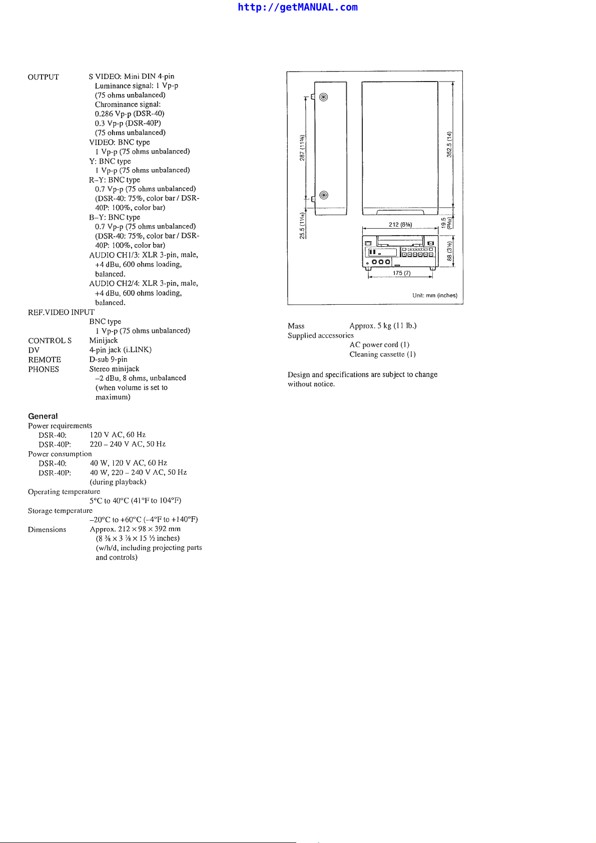
LEAKAGE TEST
The AC leakage from any exposed metal part to earth ground
and from all exposed metal parts to any exposed metal part having
a return to chassis, must not exceed 0.5 mA (500 microamperes).
Leakage current can be measured by any one of three methods.
1. A commercial leakage tester, such as the Simpson 229 or RCA
WT -540A. Follow the manufacturers' instructions to use these
instruments.
2. A battery-operated A C milliammeter . The Data Precision 245
digital multimeter is suitable for this job.
3. Measuring the voltage drop across a resistor by means of a
VOM or battery-operated AC voltmeter. The “limit” indica-
tion is 0.75V, so analog meters must have an accurate low-
voltage scale. The Simpson 250 and Sanwa SH-63T rd are ex-
amples of a passive VOM that is suitable. Nearly all battery
operated digital multimeters that have a 2V A C range are suit-
able. (See Fig. A)
AC
0.15 µF
1.5 k
Ω
Earth Ground
Voltmeter
(0.75 V)
Fig. A Using AC voltmeter to check AC leakage
– 3 –
Page 4
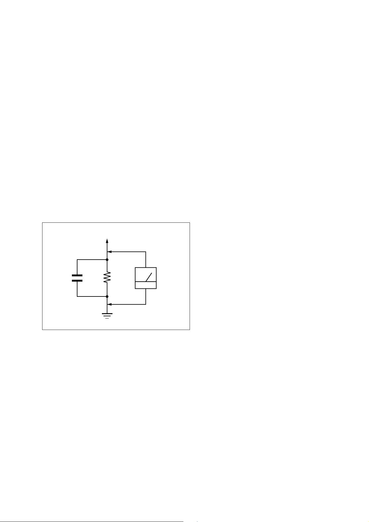
SERVICE NOTE
• Note for Repair
Make sure that the flat cable and flexible board are not cracked or bent at the terminal.
Do not insert the cable insufficiently nor crookedly.
Cut and remove the part of gilt
which comes off at the point.
(Take care that there is some pieces of gilt left inside.)
– 4 –
Page 5

TABLE OF CONTENTS
Section Title Page Section Title Page
SERVICE NOTE .................................................................... 4
1. GENERAL
Features................................................................................ 1-1
Notes on Video Cassettes..................................................... 1-1
Notes on Recording /Playing................................................. 1-1
Location and Function of Parts ......................................... 1-2
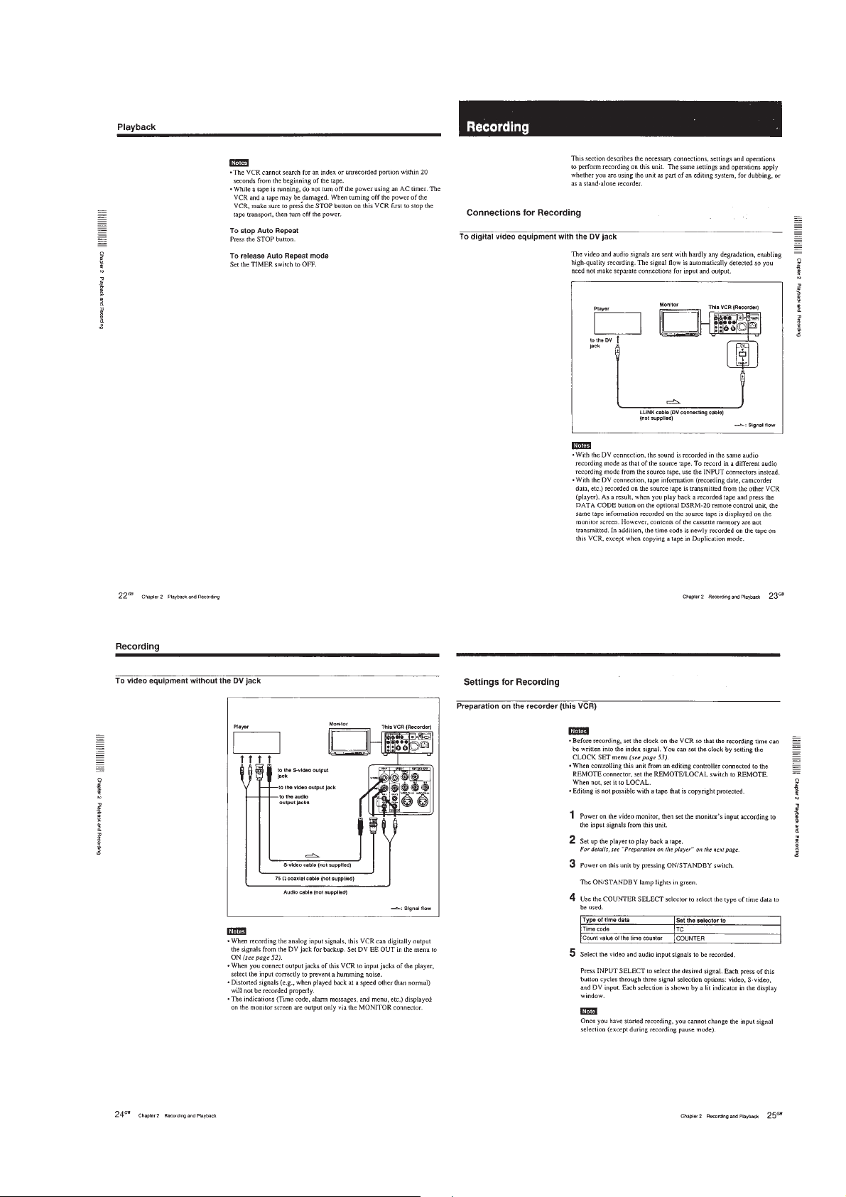
Playback ............................................................................... 1-3
Connections for Playback ..................................................... 1-3
Settings for Playback............................................................. 1-4
Playback Procedure .............................................................. 1-4
Playback Functions ............................................................... 1-4
Recording ............................................................................. 1-5
Connections for Recording.................................................... 1-5
Setting for Recording............................................................. 1-5
Recording Procedure ............................................................ 1-6
Notes on Usage in the Editing System ............................. 1-7
Connections for a Digital Non-linear Editing ................... 1-7
Connections for a Cut Editing System ............................. 1-7
Connections for an A/B Roll Editing System................... 1-8
Adjusting an Edit Timing .................................................... 1-9
Adjusting the Sync and Subcarrier Phases ..................... 1-10
Adjusting Signals ................................................................ 1-11
Using the Unit as a Recorder
with FXE-100/100P/120/120P .............................................. 1-11
Changing Menu Settings .................................................... 1-12
Changing the SET UP MENU Settings ................................. 1-12
Menu Contents ...................................................................... 1-12
Recommended Settings in the SET UP Menu...................... 1-13
Alarm Messages .................................................................. 1-13
2. DISASSEMBLY
2-1. Removal of Upper Case .............................................. 2-1
2-2. Removal of Front Panel Assembly .............................. 2-1
2-3. Removal of VA-106 Board ........................................... 2-1
2-4. Removal of Power Block ............................................. 2-1
2-5. Removal of MD Block Assembly ................................. 2-2
2-6. Removal of CM-56 Board............................................ 2-2
2-7. Removal of JC-19 Board ............................................. 2-2
2-8. Removal of RP-228 Board .......................................... 2-2
2-9. Circuit Boards Location ............................................... 2-3
3. BLOCK DIAGRAMS
3-1. Overall Block Diagram 1.............................................. 3-1
3-2. Overall Block Diagram 2.............................................. 3-7
3-3. Overall Block Diagram 3.............................................. 3-11
4. PRINTED WIRING BOARDS AND
SCHEMATIC DIAGRAMS
4-1. Frame Schematic Diagram.......................................... 4-1
4-2. Printed Wiring Boards and Schematic Diagrams ....... 4-5
• RP-228 Printed Wiring Board ................................ 4-5
• RP-228 Schematic Diagram .................................. 4-9
• JC-19 Printed Wiring Board ................................... 4-15
• JC-19 (AD/DA CONVERTER)
Schematic Diagram ................................................ 4-19
• JC-19 (S1 AFC) Schematic Diagram..................... 4-25
• JC-19 (U1) Schematic Diagram ............................. 4-29
• JC-19 (D1) Schematic Diagram ............................. 4-34
• JC-19 (C1 SPCON) Schematic Diagram............... 4-37
• JC-19 (MODE) Schematic Diagram....................... 4-41
• JC-19 (DV IN/OUT) Schematic Diagram ............... 4-45
• JC-19 (AUDIO CORE) Schematic Diagram........... 4-50
• JC-19 (DIGITAL AUDIO) Schematic Diagram ....... 4-53
• JC-19 (AUDIO D/A, A/D CONVERTER)
Schematic Diagram ................................................ 4-58
• RE-33, CB-67 Printed Wiring Boards .................... 4-61
• RE-33, CB-67 Schematic Diagram ........................ 4-63
• VA-106 Printed Wiring Board ................................. 4-66
• VA-106 (IF) Schematic Diagram ............................ 4-71
• VA-106 (VIDEO IN) Schematic Diagram ............... 4-75
• VA-106 (VIDEO OUT) Schematic Diagram ........... 4-81
• VA-106 (UVIC, DV IN/OUT) Schematic Diagram .. 4-86
• VA-106 (MONITOR OUT) Schematic Diagram...... 4-89
• VA-106 (HI CON) Schematic Diagram................... 4-92
• VA-106 (SG SELECT, EVR) Schematic Diagram.. 4-95
• RS-80 Printed Wiring Board .................................. 4-97
• RS-80 Schematic Diagram .................................... 4-99
• FR-158 Printed Wiring Board................................. 4-103
• FR-158 Schematic Diagram................................... 4-105
• GL-10 Printed Wiring Board................................... 4-109
• GL-10 Schematic Diagram..................................... 4-111
• HP-118 Printed Wiring Board ................................ 4-116
• HP-118 Schematic Diagram .................................. 4-119
• CM-56 Printed Wiring Board .................................. 4-123
• CM-56 Schematic Diagram .................................... 4-127
• MD-63, MD-64, MD-65, FP-406
Printed Wiring Boards ............................................ 4-132
• MD-63, MD-64, MD-65, FP-406
Schematic Diagram................................................ 4-135
• U-1 Printed Wiring Board ....................................... 4-137
• U-1 Schematic Diagram ......................................... 4-138
• U-2 Printed Wiring Board ....................................... 4-141
• U-2 Schematic Diagram ......................................... 4-142
5. ADJUSTMENTS
5-1. MECHANICAL SECTION ADJUSTMENTS................ 5-1
5-1-1. Information ............................................................. 5-1
1-1. How to Search Reference Pages for Removal ........... 5-1
1-2. Phase Adjustment Mark “ PH- ” .................................. 5-1
5-1-2. Preparation for Mechanical Check,
Adjustment and Maintenance ................................ 5-2
2-1. FL Block Assembly................................................. 5-2
2-2. Cassette Positions.................................................. 5-2
2-3. Loading/Unloading ................................................. 5-3
2-4. Manual Up/Down the FL Block .............................. 5-3
2-5. Service Jigs List ..................................................... 5-4
5-1-3. Phase Adjustments ................................................ 5-6
3-1. Phase Adjustment
(Loading/Unloading Driving Section) ..................... 5-6
3-2. Phase Adjustment
(S/L Cassette Selection Section)........................... 5-8
3-3. Phase Adjustment
(Mechanism Chassis Upper Surface Parts) .......... 5-10
5-1-4. Periodic Check and Maintenance .......................... 5-12
4-1. Cleaning of Rotary Drum Assembly ...................... 5-12
4-2. Cleaning of Tape Path System............................... 5-12
4-3. Periodic Checks ..................................................... 5-13
5-1-5. Mechanism Section Checks and Replacements... 5-14
5-1. Tape Stopper, Motor FPC Assembly and
Elastic Connector ................................................... 5-14
5-2. Drum Assembly and Drum Base ........................... 5-14
5-3. LM Cover, LM Worm Wheel, LM Holder and
LM Motor Assembly ............................................... 5-15
5-4. TG3/4 Catcher Block Assembly,
Pinch Driving Gear and TC Arm Assembly ........... 5-15
5-5. Pinch Arm Assembly, Pinch Limiter and
Tension Coil Spring (Pinch) ................................... 5-16
5-6. HC Arm, HC Roller Assembly,
Pinch Retainer, Pinch Cam Gear and
TG5/6 Catcher Block Assembly............................. 5-16
5-7. RL Arm and RL Link............................................... 5-17
5-8. Gooseneck Guard and Gooseneck Arm Assembly 5-17
5-9. Tension Coil Spring (TG2), Spring Adjustor,
TG2 Spring Hook, TG2 Selection Arm and Damper
Sheet ...................................................................... 5-18
5-10. Tension Coil Spring (TG7), Spring Adjustor and
TG7 Spring Hook ................................................... 5-18
– 5 –
Page 6

Section Title Page Section Title Page
5-11. TG2 Retainer, TG2 Arm Assembly (TG2 Plate Spring
and ET Magnet), S Tension Regulator Band Assembly
and TG2 Laod Arm Assembly ................................ 5-19
5-12. TG7 Retainer, TG7 Arm Assembly (TG7 Plate Spring
and ET Magnet), T Tension Regulator Band Assembly
and TG7 Load Arm Assembly ................................ 5-20
5-13. S Reel Table Block Assembly ................................ 5-21
5-14. T Reel Holder and T Reel Table Block Assembly .. 5-22
5-15. S Reel Plate Assembly ........................................... 5-22
5-16. T Reel Plate Assembly........................................... 5-24
5-17. TG1/8 Base Assembly, S Brake and T Ratchet..... 5-25
5-18 TG3/6 Roller Assembly and TG3/6 Lock Spring.... 5-26
5-19. FL Joint Gear, TG5/6 Retainer and
Capstan Motor........................................................ 5-26
5-20. FL Selection Arm, FL Relay Gear and FL Joint Arm
Assembly ................................................................ 5-27
5-21. Rotary Switch, TC Gear and Relay Gear .............. 5-27
5-22. GL Arm Retainer and GL Arm ............................... 5-28
5-23. M Slider and M Slider Arm ..................................... 5-28
5-24 . TG7 Selection Arm, TG7 Cam Gear and
T Cam Gear............................................................ 5-28
5-25. Main Cam, TG2 SL Arm Assembly and
Tension Coil Spr ing (TG2 SL) ................................ 5-29
5-26. TG3/4 Arm Block Assembly (TG3/4 Arm Assembly,
TG3/4 Limiter Spring and TG3/4 Gear), TG3/4 Base
Block Assembly (TG3/4 Base Assembly) .............. 5-30
5-27. TG5/6 Arm Block Assembly (TG5/6 Arm Assembly,
TG5/6 Limiter Spring and TG5/6 Gear), TG5/6
Base Block Assembly (TG5/6 Base Assembly)..... 5-32
5-28. Reel Motor.............................................................. 5-34
5-29. RS Arm Assembly .................................................. 5-34
5-30. RS Gear Assembly, Mic Press Spring and
Mic Lever ................................................................ 5-34
5-31. Rack Joint Gear, Rack Holder, Mic Holder,
Rack (LC) and Rack (SC) ...................................... 5-35
5-32. Plate Link Assembly............................................... 5-36
5-33. Roller Shaft Assembly and Roller Belt................... 5-38
5-34. Lid Opener.............................................................. 5-39
5-35. C Door .................................................................... 5-40
5-36. Damper Arm and Tension Spring (DB) .................. 5-40
5-37. Gear (A), Gear (B), and C Worm ........................... 5-40
5-38. Tension Coil Spring (HS), Tension (DB), Shift Plate
Spring and C Sloat Block Assembly ...................... 5-41
5-1-6. Adjustments and Checks ....................................... 5-42
6-1. Adjustment Position ............................................... 5-42
6-2. Adjustment Order ................................................... 5-43
6-3. Adjustment and Checking Method......................... 5-44
6-3-1. Reel Table Height Adjustment................................ 5-44
6-3-2. TG2/TG7 Height Adjustment.................................. 5-45
6-3-3. FWD/RVS Position Adjustment.............................. 5-45
6-3-4. TG2/TG7 Electric Tension Regulator Adjustment.. 5-46
6-3-5. FWD/RVS Back Tension Adjustment ..................... 5-48
6-3-6. Adjustment Preparations and
RF Wavef orm Check .............................................. 5-49
6-3-7. Tracking Adjustment ............................................... 5-50
6-3-8. Tracking Check ....................................................... 5-51
6-3-9. CUE and REV Check............................................. 5-52
6-3-10. Rising Check .......................................................... 5-53
6-3-11. Tape Path Check .................................................... 5-54
5-2. SERVICE MODE ......................................................... 5-55
5-2-1. Adjusting Remote Commander.............................. 5-55
1. Used Adjustment Remote Commander................. 5-55
2. Precautions Upon Using The Adjusting Remote
Commander............................................................ 5-55
5-2-2. Data Processing..................................................... 5-56
5-2-3. Service Mode ......................................................... 5-57
1. Emergence Memory Address ................................ 5-57
1-1. EMG Code (Emergency Code) .............................. 5-57
5-3. VIDEO SECTION ADJUSTMENTS ............................ 5-58
3-1. Preparations Before Adjustment............................ 5-58
3-1-1. Equipment Used..................................................... 5-58
3-1-2. Connection of Equipment ....................................... 5-58
3-1-3. Adjusting Connectors (RP 228 Board CN775)...... 5-59
3-1-4. Checking the Input Signals .................................... 5-60
1. S Video Input .......................................................... 5-60
2. Video Input ............................................................. 5-60
3-1-5. Alignment Tapes ..................................................... 5-61
3-1-6. Input/Output Level and Impedance ....................... 5-62
3-2. Power Supply System Adjustment ......................... 5-62
1. Power Supply Voltage Check,
Power Block (U-2 Board)........................................ 5-62
2. Video/Audio Block Power Supply Voltage Check,
Power Block (U-2 Board)........................................ 5-62
3-3. System Control System Adjustment ...................... 5-63
1. Initializing the C, D, E Page Data........................... 5-63
2. Input of C Pge Initial Data...................................... 5-63
3. Input of D Pge Initial Data...................................... 5-63
4. Input of E Pge Initial Data ...................................... 5-63
5. Modification of C, D, E Page Data ......................... 5-63
6. Page C Address List .............................................. 5-64
7. Page D Address List .............................................. 5-64
8. Page E Address List............................................... 5-65
3-4. Servo System Adjustments.................................... 5-66
1. Switching Position Adjustment (CM-56 Board) ..... 5-66
2. Capstan FG Duty Adjustment (CM-56 Board)....... 5-66
3-5. Video System Adjustments .................................... 5-67
3-5-1. RP-228 Board Adjustments ................................... 5-67
1. Recording Current Adjustment (RP-228 Board).... 5-67
2. PLL fo Adjustment (RP-228 Board) ....................... 5-67
3. CLK Delay Adjustment (RP-228 Board) ................ 5-68
4. AGC Center Level Adjustment (RP-228 Board) .... 5-68
5. AEQ Adjustment (RP-228 Board) .......................... 5-69
6. PLL Capture Range Adjustment
(RP-228 Board) ...................................................... 5-70
7. IC774 41.85 MHz VCO Check (RP-228 Board) .... 5-70
3-5-2. JC-19 Board Adjustments...................................... 5-71
1. A/D Converter Reference Voltage Adjustment 1
(JC-19 Board)......................................................... 5-71
2. A/D Converter Reference Voltage Adjustment 2
(JC-19 Board)......................................................... 5-71
3. Y Signal Clamp Reference Voltage Adjustment
(JC-19 Board)......................................................... 5-71
4. CR Signal Clamp Reference Voltage Adjustment
(JC-19 Board)......................................................... 5-71
5. CB Signal Clamp Reference Voltage Adjustment
(JC-19 Board)......................................................... 5-71
6. Playback Y Signal Level Adjustment
(JC-19 Board)......................................................... 5-72
7. Playback CR Signal Level Adjustment
(JC-19 Board)......................................................... 5-72
8. Playback CB Signal Level Adjustment
(JC-19 Board)......................................................... 5-73
9. IC422 27MHz XTAL fo Adjustment (JC-19 Board) 5-73
10. AFC Preliminary Adjustment (JC-19 Board) ......... 5-73
11. AFC Picture Frame Adjustment (JC-19 Board) ..... 5-74
12. AFC Adjustment (JC-19 Board) ............................. 5-74
3-5-3. General Adjustments .............................................. 5-75
1. Playback Y/CR Delay Adjustment
(VA-106 Board)....................................................... 5-75
2. Playback Y/CB Delay Adjustment
(VA-106 Board)....................................................... 5-75
3. Playback Y Signal Level Adjustment
(VA-106 Board)....................................................... 5-76
4. Playback Y Setup Level Adjustment
(VA-106 Board)....................................................... 5-76
5. Playback CR Signal Level Adjustment
(VA-106 Board)....................................................... 5-77
6. Playback CB Signal Level Adjustment
(VA-106 Board)....................................................... 5-77
7. Playback Sync Level Adjustment
(VA-106 Board)....................................................... 5-78
8. Playback Carrier Balance Adjustment
(VA-106 Board)....................................................... 5-78
9. Playback Burst Level Adjustment
(VA-106 Board)....................................................... 5-79
– 6 –
Page 7

Section Title Page
10. Playback Composite Video Chroma
(R-Y Signal Level) Adjustment (VA-106 Board)..... 5-80
11. Playback Composite Video Chroma
(B-Y Signal Level) Adjustment (VA-106 Board)..... 5-80
12. Playback Composite Video Chroma
(R-Y Phase) Adjustment (VA-106 Board).............. 5-81
13. INT Subcarrier Frequency Adjustment
(GL-10 Board) ........................................................ 5-81
14. Decoder Freerunning Frequency Adjustment
(VA-106 Board) ....................................................... 5-81
15. Recording Y/CR Delay Adjustment
(VA-106 Board) ....................................................... 5-82
16. Recording Y/CB Delay Adjustment
(VA-106 Board) ....................................................... 5-82
17. Recording Y Signal Level Adjustment
(VA-106 Board) ....................................................... 5-83
18. Recording Chroma Decoder HUE Adjustment
(VA-106 Board) ....................................................... 5-83
19. Recording CR Signal Level Adjustment
(VA-106 Board) ....................................................... 5-84
20. Recording CB Signal Level Adjustment
(VA-106 Board) ....................................................... 5-84
21. SYNC Position Adjustment (GL-10 Board)............ 5-85
22. EXIT Subcarrier Phase Adjustment
(GL-10 Board) ........................................................ 5-85
23. Burst Position Adjustment (GL-10 Board) ............. 5-86
24. Y/C Separation Adjustment (VA-106 Board) ......... 5-86
25. OSD1 Subcarrier Adjustment (VA-106 Board) ...... 5-87
26. OSD2 Subcarrier Adjustment (VA-106 Board) ...... 5-87
3-5-4. BIST Check ............................................................ 5-88
1. Playback System Check
(JC-19, RP-228 Boards) ........................................ 5-88
2. Record System Check ........................................... 5-89
3-6. Audio System Adjustments .................................... 5-90
1. E-E Level Check..................................................... 5-90
2. Playback Level/Indicator Check ............................. 5-90
3. Recording/Playback Check (Audio Lock Mode) .... 5-91
3-7. Arrangement Diagram for Adjustment Parts.......... 5-92
6. REPAIR PARTS LIST
6-1. Exploded Views ........................................................... 6-1
6-1-1. Overall Assembly ................................................... 6-1
6-1-2. Chassis Assembly.................................................. 6-2
6-1-3. MD Block Assembly ............................................... 6-3
6-1-4. FL Cassette Compartment Assembly.................... 6-4
6-1-5. Mechanism Chassis Assembly (1)
(Top Side View (1))................................................. 6-5
6-1-6. Mechanism Chassis Assembly (2)
(Top Side View (2))................................................. 6-6
6-1-7. Mechanism Chassis Assembly (3)
(Top Side View (3))................................................. 6-7
6-1-8. Mechanism Chassis Assembly (4)
(Bottom Side View (1)) ........................................... 6-8
6-1-9. Mechanism Chassis Assembly (5)
6-2. Electrical Parts List ..................................................... 6-10
Hardware List ........................................................................ 6-48
(Bottom Side View (2)) ........................................... 6-9
– 7 –
Page 8
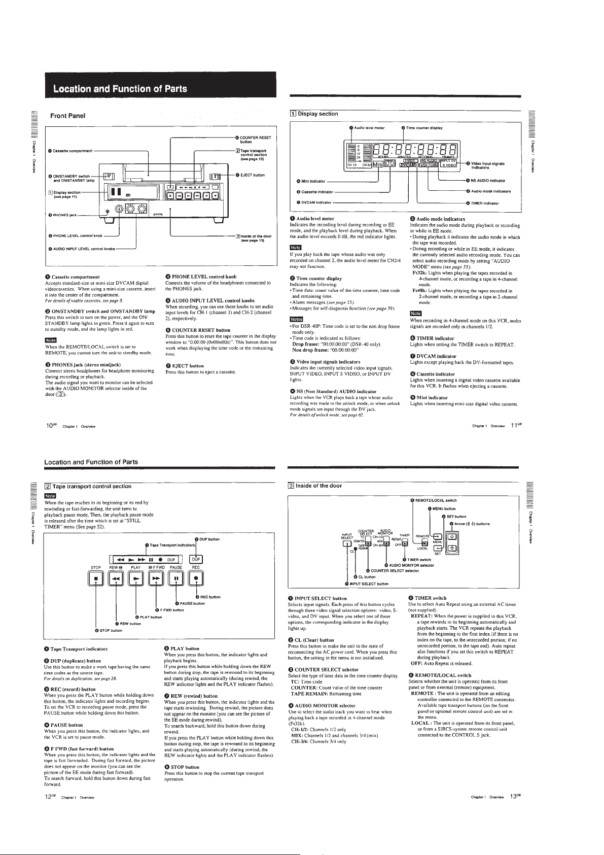
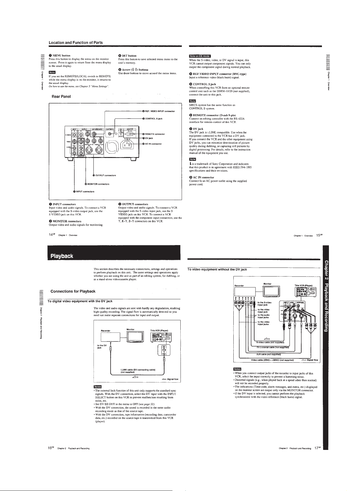
SECTION 1
GENERAL
DSR-40/40P
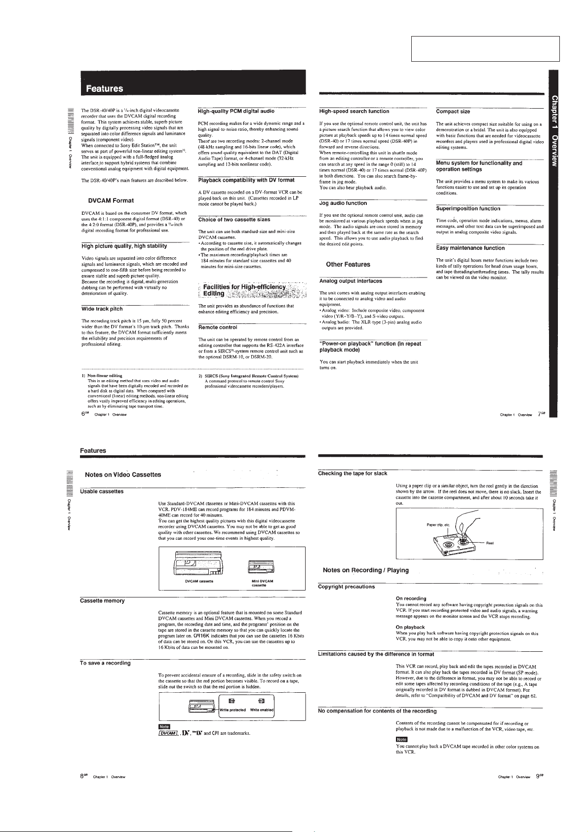
This section is extracted from DSR40/40P instruction manual.
1-1
Page 9
1-2
Page 10
1-3
Page 11
1-4
Page 12
1-5
Page 13
1-6
Page 14
1-7
Page 15
http://getMANUAL.com
1-8
Page 16
1-9
Page 17
1-10
Page 18
1-11
Page 19
1-12
Page 20
1-13 E
1-13
Page 21
SECTION 2
4 Two sumitite
screws (B3)
5 Power block
3 Harness
(CN13)
2 Two harnesses
(CN10, 11)
1 Harness
(CN1)
DISASSEMBLY
Note: Follow the disassembly procedure in the numerical order given.
2-1. REMOVAL OF UPPER CASE 2-3. REMOVAL OF VA-106 BOARD
3 Open sides of upper case and
1 Two case screws
(M3)
remove the one in the direction
of the arrow A.
A
1 Two flat cables
(CN851, 856)
8 Two sumitite
screws (B3)
9 Remove the
VA-106 board in the
direction of the arrow.
2 Two flat cables
(CN101, 102)
3 Two flat cables
(CN001, 852)
4 Harness
(CN601)
5 Flat cable
VA-106 board
DSR-40/40P
(CN401)
7 Two sumitite
screws (B3)
6 Harness
(CN855)
2-2. REMOVAL OF FRONT PANEL
3 Two claws
2 Two case screws
(M3)
2-4. REMOVAL OF POWER BLOCK
ASSEMBLY
4 Front panel
assembly
2 Two claws
1 Two sumitite screws
(B3)
2-1
Page 22
2-5. REMOVAL OF MD BLOCK ASSEMBLY 2-7. REMOVAL OF JC-19 BOARD
4 Two sumitite
screws (B3)
8 Harness
(CN004)
2 Two sumitite
screws (B3)
3 Cassette
Compartment
support
6 MD block
assembly
7 Three harnesses
(CN101, 701, 831)
5 Two sumitite
screws (B3)
1 Two flat cables
(CN103, 104)
7 JC-19 board
4 Claw
2 Two flat cable
(CN411, 412)
JC-19 board
3 Claw
1 Harness
(CN501)
5 Four screws
(P2.6 × 5)
6 Two shield
cases
2-6. REMOVAL OF CM-56 BOARD
3 Flat cable
(CN003)
6 Two claws
5 Sumitite screw
(B3)
CM-56 board
7 CM-56 board
2 Harness
1 Three flat cables
(CN005, 007, 008)
(CN002)
2-8. REMOVAL OF RP-228 BOARD
5 RP-228 board
RP-228 board
1 Flat cable
(CN003)
4 Two tapping screws
(2 × 4.5)
2 Special tapping
screw
3 JC support
4 Two flat cables
(CN001, 006)
2-2
Page 23
2-9. CIRCUIT BOARDS LOCATION
GL-10
(SYNC GENERATOR)
MD-65
(TAPE DETECT)
MD-63
(TAPE DETECT)
HP-118
(AUDIO)
FR-158
(DISPLAY CONTROL)
U-2
RP-228
(POWER 2)
(REC/PB AMP)
MD-64
(TAPE DETECT)
RS-80
(RS-422A IF)
VA-106
IF, VIDEO IN/OUT, UVIC,
DV IN/OUT, MONITOR OUT,
HI MICOM, RS MICOM
U-1 (POWER 1)
JC-19
AD/DA CONVERTER, S1 AFC, U1,
D1, C1 SPCON, MODE, DV IN/OUT,
AUDIO CORE, DIGITAL AUDIO,
AUDIO D/A, A/D CONVERTER
CM-56
(SERVO, SYSTEM CONTROL)
RE-33
(V/A IN/OUT)
CB-67 (AUDIO OUT)
2-3
2-3 E
Page 24
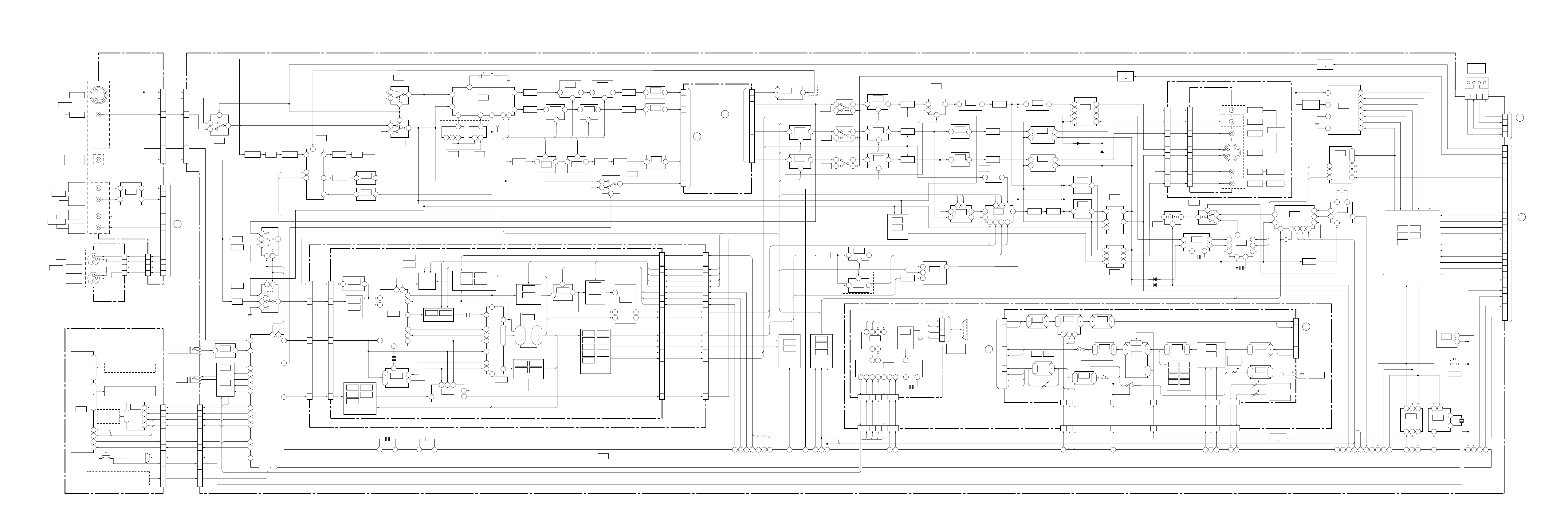
3-1. OVERALL BLOCK DIAGRAM 1
DSR-40/40P
SECTION 3
BLOCK DIAGRAMS
INPUT
MONITOR
OUTPUT
S VIDEO
INPUT
VIDEO
REF, VIDEO
INPUT
AUDIO
CH1
AUDIO
CH2
AUDIO
CH1/3
AUDIO
CH2/4
AUDIO
CH1/3
AUDIO
CH2/4
FR-158 BOARD
(SEE PAGE 4-105~107)
DRIVER
RE-33 BOARD (1/2)
(SEE PAGE 4-63~65)
J1 (1/2)
J3 (1/2)
CN102
CB-67 BOARD
(SEE PAGE 4-65)
1
ı
4
FF,REW, STOP, PLAY, DUP,
10
COUNTER RESET, PAUSE, REC
ı
13
15
ı
32
FLUORESCENT INDICATOR TUBE
35
39
ı
LED
44
IC104
FL
DUP, REC,
PAUSE, FF,
REW, PLAY
1
8
2
6
5
9
S101
FUNCTION KEY
AUDIO MONITOR, INPUT SELECT, UP,
DOWN, POWER, EJECT, TIMER,
COUNTER SELECT, SET, MENU
A OUT LX
A OUT LY
A OUT RX
A OUT RY
IC103
LED
DRIVER
BZ101
BUZZER
7
10
12
11
14
A IN L
A IN R
A OUT L
A OUT R
1
2
4
5
CN104
5
IC1
AMP
3 1
CN101 CN3
1
2
4
5
FUNCTION KEY
ND101
1
ı
6
MAIN
RESET
CN1
(1/2)
CN2
1
2
22
20
24
SDC DET
26
REF IN
18
1
3
5
7
9
10
12
13
CONTROL S
18
17
13
DATA FROM HI
15
19
12
11
5
20
ı
25
30
C-IN
5
Y-IN
7
V-IN
3
1
9
A
HP-118 BOARD
CN201
(SEE PAGE 3-3)
LANC
LED RST
LED CS
HI SCK
DATA TO HI
FLD CS
BUZZER
RESET
KEY0-5
POWER SW
VA-106 BOARD
(SEE PAGE 4-71~96)
CN401
(1/2)
3
1
S-Y/VIDEO SWITCH
CN851
13
14
18
16
12
19
20
26
1
6
ı
11
2
7
IC201
IC853
2 4
INVERTER
IC860
LANC OUT
IC855
MULTI
PLEXER
1
2
33
44
55
BUFFER CLAMP
L.P.F
IC0001
SIGNAL
SELECT
IC0002
SIGNAL
SELECT
B.P.F
33
6
3
4
25
26
29
27
30
46
47
48
18
62
L.P.F
3
1
5
4 2
4 2
5
1
3
91–96 99
Q102
3V 5V
TP201
G10
E6
23
31
10
26
IC1124
SYNC GEN
14.3MHz : DSR-40
17.7MHz : DSR-40P
IC204
VC DELAY
IC212
6
VC DELAY
G2
4
IC207
1
E5
E1, E2, E4, E6, E8
E6, E8
6
3
4
G6G5G4
1
3
3
2
IC1135
EX OR
E7
4
IC208
VC AMP
4
20
TRAP
19
TRAP
G9
C1
IC1128
IC1132
SC PHASE ADJ
IC1121
BUFFER
3
11
5
13
9
15
12
17
IC1143
IC1144IC1142
DELAY
6
VC DELAY
12
14
16
18
DL202 FL204 DL201
2
2
4
ı
6
6
8
*IC1105, IC1143 :
DSR-40 ONLY
IC1105
3
1
G1
3
IC1115
IC1126
1
IC214
VC AMP
3
5
C4
IC1133
IC1137
HD PHASE
90 SHIFT
TIMING DELAY
PULSE STRECH
IC206
VC AMP
3
5
G3
1
3
2
IC1129
IC1131IC1117
IC1134IC1120
IC1139IC1123
IC854
HI CON
5
FL203
FL205
IC217
SYNC SELECT
7
CN1001 (2/2)
4
IC1138
0/180 LALT
1
9
GL-10 BOARD
(SEE PAGE 4-111~114)
3
6
CN102
(1/2)
CR-IN
IC209
3
3
AMP
IC218
AMP
1
10
CB-IN
1
8
B
JC-19 BOARD
CN104
(SEE PAGE 3-7)
B
JC-19 BOARD
CN104
(SEE PAGE 3-7)
Y-IN
IC215
3
AMP
12
ı
15
C3
8
C1
9
C4
10
C3
11
1
16
2
18
3
19
5
6
20
21
22
24
25
23
1
12
AFCY
7
H PHASE BIT 1-4
EVER 23 H PHASE FINE
EVER 24 SC PHASE
EVER 25 SC V PHASE
EVER 22 SC FREE FREQ
SC ON
INDI EE
SC 0/180
SC U
SC V
R BF OUT
R SYNC OUT
R Y BLK
R Y CLAMP
R UV CLAMP
GEN REF Y
16
ı
19
23
22
21
20
15
13
12
26
25
11
10
9
7
6
8
CN0001
(2/2)
C3
C1
C4
C3
87 82 64 84 85 86 60 100 2 51 52 22 23 19 12 57 58 59 97 98 16 14 10 17 65 32 2483
16
23
21
19
CN102
(2/2)
XYC SEP
Y OUT
1
2
1
CR OUT
2
CB OUT
1
2
9
10
(1/2)
IC104
BUFFER
6
6
1
2
IC1115
IC1116
AND GATE
8
IC402
VC DELAY
4
B2
IC403
VC DELAY
4
B3
1
2
*DSR-40P ONLY
IC404
Y SWICH
3
IC405
R-Y SWICH
3
IC406
B-Y SWICH
FL402
B2-16, C1-4,
G1-10, O1
IC1105
IC1110
IC1114
D/A
CONVERTER
IC409
Y BLANKING
B13
B4
B5
3
7
1
614KHz
X1
8MHz
SET UP ADD
2
4
6
IC407
VC AMP
CN2
1
2
3
4
X2
IC412
4
16
INVERT AMP
IC413
3
1
AMP
IC414
3
1
AMP
B9
B8
2 6
2
7
5
7
2
8
3
REMOTE
RS-422A
IC420
VC AMP
3
5
RE-33 BOARD
(SEE PAGE 3-1)
DL401
1
IC424
INVERTER
2
B10
4
IC422
1
C ENCODE
24
5 20 3 22
1212
A
CN2
4
B11
21 17
1
3
5
7
9
10
12
13
18
CN201
A IN L
A IN R
A OUT L
A OUT R
A OUT LX
A OUT LY
A OUT RX
A OUT RY
IC418
4
INVERT AMP
IC410
2
R-Y OUT
6
DRIVER
IC408
2
B-Y OUT
6
DRIVER
FL403 B.P.F
3
IC704
5
BUFFER
IC204
AUDIO AMP
1
7
RV201
RV202
2
4
6
14
4
4
IC708
10
7
AUDIO
PROCESS
3 12 13
312
Q710
Q711
MUTE
1
7
312
546 1483 12 1311 15
A XVR CS
A XVR SO
A XVR SCK
546 1483 12 1311 15
1
2
IC415
Y OUT
DRIVER
IC421
INVERT
AMP
IC426
INVERT
AMP
8
5
IC201
BUFFER
1
1
3
5
13
7
16
10
1
7
2
6
IC715
BUFFER
IC716
BUFFER
Q201
Q202
MUTE
1
7
IC205
1
3
5
CN200
CN856
13
14
13
14
7
2
7
2
7
2
IC411
VC AMP
B6
B7
3
IC416
VC AMP
1
VC AMP
3
B14
IC428
1
VC AMP
3
B16
IC429
1
VC AMP
3
B15
1
5
3
2
5
*DSR-40P
ONLY
3
1
3
1
3
1
1
1
IC427
CLAMP
5
CLAMP DL402
5
CLAMP DL403
5
IC401
IC430
INVERT AMP
FL401
RS-80 BOARD (SEE PAGE 4-99~101)
123
4
65 7
8
IC3
INTERFACE
2 3
86 87
RS-422A CONTROL
21 20 22 23 24 26 9 87
CN1
54789106
RS TXD
RS SCK
RS RXD
RS LANC IN
RS LANC OUT
6743215
234
1
2
CN852
1
5
IC1
RS CS
RS-422
CLOCK
DRIVER
RS RST
IC2
85
IC205
S-C/C SWITCH
3
7
1
2
2
3
7
1
IC211
Y/C SEP
79
25 39
G7
33
G8
41
7
1
2
LOCK Y
30
CN0001
(1/2)
7
2
1
8081
34
45
49
28
14
24
LOCK C
INT/EXT
LOCK
PHASE
GEN
GEN
IN
GEN
FL201
31
11
CN1001
(1/2)
1
3
17
7
FL202
2
*IC1112 :
DSR-40 ONLY
B.P.F
IC202
3 1
AMP
IC210
4 1
OSC
IC1101
1
SYNC SEP
IC1102
IC1106
SC PROC
IC1104
IC1111
IC1107
IC1112
IC1108
COUNTER
SHIFT REGISTER
17
4
11
X1101
E7, E9
42
S-Y/Y SWITCH
IC1109
GEN LOCK
8
IC1103
9
11
IC203
IC1116
IC1119
HD SHIFT
FINE ADJ
15 20
18
14
1
8
10
19
9
14.3MHz : DSR-40
14.1MHz : DSR-40P
6
12
1
NOR
X851
20MHz
43
1
IC1113
SC SWITCH AMP
54
C3
55
IC216
*DSR-40P ONLY
2
C2
IC1118
1824 13
IC1141
SYNC GEN
X853
32.798KHz
10
5
25
28
1
91312
IC1122
IC1127
HD SHIFT COURSE ADJ
X1102
14.3MHz : DSR-40
17.7MHz : DSR-40P
21
229
X201
CT201
IC213
C DECODE
24 18 4 11
4
12
IC219
IC1125
IC1130
17
8
29
22
13
18
7
24
15
E9
3V 5V
IC417
C OUT DRIVER
2
6
4
2
6
4
IC419
VIDEO OUT
DRIVER
1
7
2
6
P OFF MUTE
Q103
14
13
14
13
16
14
4
9 11
IC711
AUDIO
SELECTOR
Q708, Q709
MUTE
CN401
IC654
MONITOR OUT
DRIVER
13
3
12
5
A FIL ON
Y OUT
22
R-Y OUT
24
B-Y OUT
26
SY OUT
20
SC OUT
18
MONITOR
OUT
14
V OUT
16
13 2
14
IC706
1
7
BUFFER
IC705
IC707 IC714
IC709 IC717
IC710 IC718
FILTER
RE-33 BOARD(2/2)
(SEE PAGE 4-63~65)
CN1
5
3
1
7
9
13
11
IC653
OSD SELECT
7
2 9
IC423
SYNC SEP
8
10 11
3
5
IC713
J2
J3 (2/2)
J4
J1 (2/2)
2
3 25
1
25
12
5
X401
500KMz
IC702
IC703
AUDIO
SELECTOR
A MON2
A XGAIN UP
A MON1
IC425
13
OSD1
3
98
X402
14.3MHz : DSR-40
17.7MHz : DSR-40P
B12
HP-118 BOARD
(SEE PAGE 4-119~122)
RV1
PHONE
LEVEL
RCH REC VR
LCH REC VR
Y
R-Y
B-Y
S VIDEO
VIDEO
VIDEO
22
23
24
1
7
BUFFER
5
3
HP AMP
OUTPUT
MONITOR
OUTPUT
3 65
1
2
3
IC701
3
5
IC1
6
1
L REC LEVEL
R REC LEVEL
Q101
3V 5V
IC651
OSD2
8
X651
14.3MHz : DSR-40
17.7MHz : DSR-40P
O1
CN701
A REC L
A REC R
A PB L
A PB R
RV2
RV3
Q613
SYNC SEP
X601
3.58MHz : DSR-40
4.43MHz : DSR-40P
1
2
3
12
13
2423229
123
L.P.F
8
6
C
JC-19 BOARD
CN831
(SEE PAGE 3-9)
4
2
PHONES
18
17 11
IC602
U VIC CONTROL
31
32
IC106
AND GATE
3
6
11 12
10 11
IC652
9
SYNC SEP
5 8
2
4
1
4
13
2
5
X652
500KMz
3
3
10
12
13
29
28
IC101
IC104
(2/2)
IC102
IC105
IC103
AND GATE/INVERTER
4 3 2
IC856
EEP ROM
1 6 7 5
4
35 36 37 20 21 7 31 40 63 38 39
7 6
IC858
CLOCK GEN
IC859
RESET
CN602
S851
RESET
X852
0.032MHz
2
3
8
6
DV
IN/OUT
1234
TPB
NTPB
PB/XEE
OSD SCK
OSD SO
UVIC GATE
UVIC SWIN
UVIC BUSY
XCS UVIC
MO XPFAIL
XWAKEUP
TPA
NTPA
S/XV
XCS
MO SI
MO SO
MO SCK
MO RST
XCS MO
HI SI
HI SO
HI SCK
XHI RST
MO
JOG FIL
CN601
CN101
2
3
5
6
7
6
11
12
10
14
15
16
17
18
19
20
21
23
24
25
26
29
28
27
2
D
JC-19 BOARD
CN701
(SEE PAGE 3-8)
E
JC-19 BOARD
CN103
(SEE PAGE 3-9)
3-1 3-2 3-3 3-4 3-5
Page 25
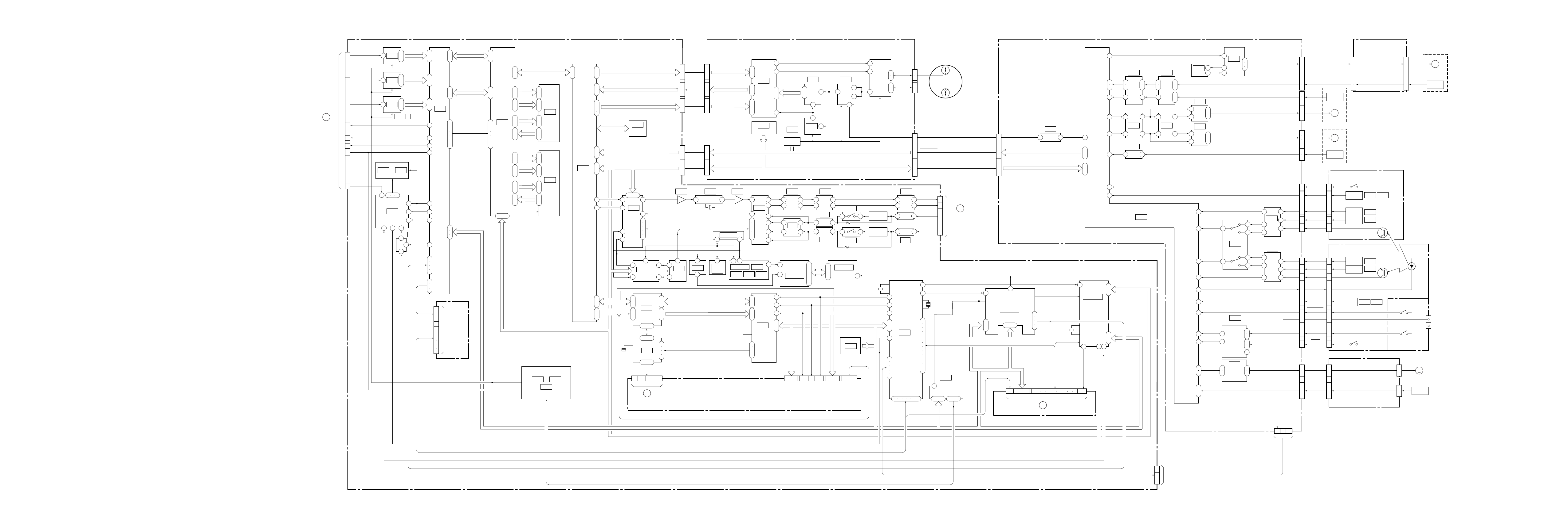
DSR-40/40P
3-2. OVERALL BLOCK DIAGRAM 2
B
VA-106 BOARD
CN102
(SEE PAGE 3-2,3)
19
21
23
8
12
10
15
24
CN104
Y-IN
CR-IN
CB-IN
Y-OUT
CB-OUT
CR-OUT
XYCSEP
AFCY
21
IC017
21
IC016
21
IC015
IC015 ~
A/D CONVERTER
~
IC209 IC214
TIMING GEN.
7
12 16 60
IC205
CLOCK GEN.
2252
46
1
8bit DATA 8bit DATA
ı
8
1
8bit DATA
ı
8
1
8bit DATA
ı
7
28
43
53
IC206
1
4
2
SGH, SCCK
CK135, SCOE
AND
IC017
TDI
TCK
TMS
64
ı
71
55
ı
62
46
ı
53
139
145
146
44
76
78
79
77
80
82
83
101
88
89
92
CN503
IC200
I/O
INTERFACE
16
18
20
10
ı
13
15
17
19
111
ı
118
122
ı
129
107
FLBKY, FLBKC
ı
CINV, REC, JSYC, JSYY
110
JFDE, JODE
120
130
131
166
103
104
106
FOR CHECK
8bit DATA
17
ı
26
5
ı
13
2
ı
4
16
26
ı
29
IC401
BLANKING
92–94
VRT, VRB
68
ı
84
158
ı
165
149
ı
157
142
ı
148
134
ı
141
124
ı
131
116
ı
120
109
ı
113
97
ı
106
DATA
ADDRESS
ADDRESS
DATA
DATA
ADDRESS
ADDRESS
DATA
CONTROL
16bit DATA
2
ı
9
12
ı
24
52
ı
64
67
ı
74
2
ı
9
16
ı
19
57
ı
60
67
ı
74
IC009
IC018
REF DC GEN.
JC-19 BOARD
(SEE PAGE 4-19~60)
IC403
V RAM
C
IC402
V RAM
Y
SP SI, SO, SCK
~
IC013
172
ı
189
DESHUFFLE
IC411
AV MIX
ECC
TBC
91
ı
95
81
ı
85
74
ı
77
80
62
ı
64
158
ı
160
193
198
34
ı
54
55
INPV, IOCE, IENPA
ı
57
IC410
4M
D RAM
MECHA SI, SO, SCK
SP SI, SO, SCK
70–72
60 11
58
IC805
A/D, D/A
14
CON V.
10
54
55
X701
24.6MHz
28
98
99
24
IC904 (1/2)
FS CON
25
82
ı
100
78
DV SIGNAL
ı
80
PROCESS
DV INTERFACE
2 3 5 6
VA-106 BOARD
(SEE PAGE 3-5)
9
LRCK, BCK, MCK, FSE1, FSE2
23
59
612835
2
ı
20
IC701
22
ı
27
59–67
REQ, CLK, D0/1
CTL0/1
7–12
1
2
IC702
43
46
33–36
TPA, TPB
NTPA, NTPB
CN701
D
CN601
CN412
18
ISCDXI 0-4
ı
22
11
AVDXI 0-4
ı
15
6
DXO 0-4
ı
10
CN411
MECHA
20
SO/SI/SCK
ı
22
SP
14
SCK/SO/SI
ı
16
IC804
MCK
30 3
IC911
AUDIO
CLK GEN.
CNA, LPS, PWR DN, XRESET
RP-228 BOARD
(SEE PAGE 4-9~12)
CN101
9
ı
13
16
ı
20
21
ı
25
CN102
9
ı
11
15
ı
17
IC801
40 36 13 26
TIMING CONT
X801
49.152MHz
IC422 (2/2)
59 66
FLTA
FLTT
2 3 11
9
D-FFS
DATA BUS
IC901
(1/2)
INDT 0–15
IC902
ADDRESS BUS
50
ı
54
IC774
59
CHANNEL
ı
CODING
63
1
ı
4
64
IC770
2
E PROM
MECHA SI, SO, SCK
SP SI, SO, SCK
IC807 IC836
A/D, D/A CON V.
IC837
14
11
12
15
16
17
AUDIO CLOCK
IC901 (2/2)
IC907 IC909
X702
6MHz
36
51
53
57
81
83
85
IC903
ı
ı
ı
IC916
IC703
DV
CONTROL
25
27
IC772
29
ı
35
37
6 7 6 7 6 7
27
2 1
6
7 6
5
3
1 2
4
5
29
28
11
12
88
22
ı
24
CN702
2
A/D
21 20
ı
CONV
8
12
23
28
EVR
IC773
PLL
2 1
7 6
7 6
10
27
63
ı
65
93
FOR CHECK
IC838
BUFF
IC831
BUFF
BUFF
IC833
IC771
BUFF
IC835
BUFF
IC421 (2/2)
SP CON
4 – 6 8 7 3 25 – 40 22 – 24
11
ı
15
41
IC775
RF EQ
IC834
3 4
13 14
IC834
IC904 (2/2)
FS CON
MO SI, SO, SCK
IC502
2
E PROM
2
27
31
IC777
42
47
REC/PB
AMP
19
EMPHASIS
EMPHASIS
53
X501
20MHz
X/Y ODD
6
7
2
X/Y EVEN
3
PB RF
IC840
BUFF
2 1
2 3
BUFF
IC831
2 3
BUFF
IC833
15
25
24
48
ı
50
IC501
MODE
78
CONTROL
5
6
27
72
73
1 2 26 30 38 61 85
CN771
5
6
2
3
CN103
20
4
ı
6
12
ı
14
X HI RST, MO XPFAIL
DRUM HEAD
PBRF
MECHA SCK,DATA FROM MECHA,DATA TO MECHA
SP SI,SP SO,SP SCK
CN831
A. PB. L
A. PB. R
A. REC. L
A. REC. R
14
19
16
22
29
32
ı
35
45
46
55
65
67
80
81
4
2
HP-118 BOARD
8
(SEE PAGE 3-4)
6
X502
32.768kHz
IC504
D/A CONV
4
19–21 10–12
CN701
OSDSO S X/V, HI SCK, HI SO, HI SI, XCS MO, MORST, PB/XEE
OSD SCK, XCS UVIC, UVIC BUSY, UVIC SWIN, UVIC GATE, XCS OSD2
CM-56 BOARD
(SEE PAGE 4-127~130)
IC005
5 32 74
ATF
33
ı
35
60
ı
62
11
25
27
17
19
CN003
ı
ı
C
59
IC421 (1/2)
SP CON
MO RST
96
X422
27MHz
6
FRAME PLL
77
ı
79
MO SI, SO, SCK
CN103
28
TRKD, FLTD
IC422 (1/2)
7–9
2 3 11 – 13 5 – 8 10 14 – 17 19 – 21 24 25 29
2
SGH, SCCK
3
CK135, SCOE
32
33
E
X421
20MHz
VA-106 BOARD
CN101
(SEE PAGE 3-5)
43
4
15
15
4
IC019
BUFFER
IC503
CAP
MOTOR
DRIVE
IC022
REEL
MOTOR
DRIVE
78
52
51
79
28
71
26
20
19
95
96
22
ı
25
IC008
57
6
56
58
44
45
49
29
72
33
ı
35
60
ı
62
18
50
5
11
12
5V~3V
LEVEL
CONV.
3 2 12
5 7 13
IC016
LPF
3 1 4
IC014
FG
1 3
AMP
IC003
MECHA CONTROL
IC011
9
1
10
6
FG, PG
AMP
13
14
10
IC012
DC/DC
7
CONV.
18
IC021
1
DRUM
3
19
1
21
21
ı
23
21
ı
23
4
15
6
11
6
8
MOTOR
DRIVE
S
L
IC017
S
L
IC002
AND
IC009
LOADING
MOTOR
DRIVE
29
31
13
IC018
1
3
5
1
2
1
5
2
12
3
15
24
COMP
2
IC006
1
2
COMP
13 10
CN008
8
DRUM U/V/W
ı
10
CN007
CN006
12
13
3
4
5
6
13
3
10
11
12
13
FG OUT
CAP
U/V/W
REEL
U/V/W
FG OUT
FG,PG
CAP
FG
M
M
REEL
FG
MD-64 BOARD
CN005
CC DOWN SW
2
S EL OUT
4
S T REEL FG
7
5
10
1
L T REEL FG
7
TOP SENS
9
CN002
8
6
9
3
1
MD-63 BOARD
CN001
CN008
S S REEL FG
3
L S REEL FG
1
16
8
4
13
11
10
14
15
6
7
2
ı
5
END SENS
TAPE LED
T EL OUT
REC PROOF
CHIME SDA
CHIME SCK
C IN
C OUT
LM LOARD
/UNLOAD
MODE SW
A-D
7
5
CN101
14
16
1
9
S ELETEN
13
4
6
7
3
2
CN202 CN203
8
9
10
ı
13
MD-65 BOARD(1/2)
(SEE PAGE 4-136)
CN202 CN201
5
ı
7
2
3
M902
CAPSTAN
MOTOR
M904
REEL
MOTOR
(SEE PAGE 4-135,136)
S002
(CC DOWN)
T ELETEN
S T REEL
L T REEL
S S REEL
L S REEL
IC005 IC006
IC003
FG
IC004
FG
Q101
TAPE END
SENSOR
(SEE PAGE 4-134,135)
IC102
FG
IC101
FG
Q102
TAPE END
SENSOR
IC103 IC105
S101
(C OUT)
MD-65 BOARD(2/2)
(SEE PAGE 4-136)
6
11
1
2
REC
PROOF
C IN
FP-406 BOARD
(SEE PAGE 4-135)
1
2
CN204
1
ı
4
U,V,W
ı
PG,FG
TAPE
LED
CN901
M
MODE
SW
DRUM
PG FG
M903
LOADING
MOTOR
M
(FOR CASSETTE MEMORY)
M901
DRUM
MOTOR
MO SI, SO, SCK
X PARSLEY MODE, X RESET, P FAIL, X LANC PWR ON, LANC P CONT, LANC OUT, LANC IN
SGH, SCCK, CK135, SCOE
Y CLP ERR, CR CLP ERR, CB CLP ERR
SP SI, SO, SCK
C IN
CHIME SDA
CHIME SCK
CN501
2
3
5
CHIME SDA
C IN
5 2 3
CN002
CHIME SCK
3-6 3-7 3-8 3-9 3-10
Page 26
3-3. OVERALL BLOCK DIAGRAM 3
DSR-40/40P
AC INLET
AC IN
F1
CN1
3.15A/250V
1
2
U-1 BOARD
(SEE PAGE 4-138~140)
FR-158 BOARD (SEE PAGE 4-105~107)
U-2 BOARD
L1
L2
D1
Q1
SWITCH
Z1
PWM
T1
POWER TRANS
Z2
Z3
PHOTO
COUPLER
M905
FAN
MOTOR
CN3
+14V
1
2
M
(SEE PAGE 4-142~144)
CN1
1
2
CN13
SW 12V
1
Z1
1 2
+14V REG
Z2
1 2
+6V REG
Z9
1
REG
Q1
12V REG
Z7
1 2
+12V REG
4
Z5
1 2
+3.1V REG
3
5
1 2
1 2
1 2
UNSW 14V
UNSW 6V
CN10 CN11
2 3
Q2, Q4
SWITCH
5
Z8
+3.1V REG
Z6
+5V REG
4
4
Z4
+5V REG
Z10
–8V REG
14
13
15
Z4
POWER
CONTROL
Z11
2 3
–12V REG
Z12
2 3
–5V REG
1
ı
4
16
RF 5V
SW 5V
SW 3.1V
VIDEO 5V
AUDIO 5V
J 3.1V
UNSW 6V
UNSW 3.1V
VIDEO –5V
AUDIO –5V
962147313456
CN12
UNSW 14V
8
9
UNSW 6V
2
3
UNSW 3.1V
4
UNSW –8V
7
SW –12V
11
POWER CONT
1
SW 12V
VA-106 BOARD
(SEE PAGE 4-71~96)
CN855
8
9
2
3
4
7
11
1
B UP 5V, D5V
2
IC862
1 3
+5V REG
IC861
2 3
–5V REG
IC103
IC101
AND/BUFFER
IC106
IC104IC102
BUFFER/AND
IC1116
IC1115
AND
D/A CONVERTER
* IC416 : DSR-40P ONLY
IC1114IC1110IC1105
IC651
IC425
OSD
IC652
IC423
SYNC SEP
IC653
OSD SELECT
IC602
UVIC CONTROL
IC416
IC411IC407
VC AMP
IC212IC207IC204
IC403IC402
VC DELAY
IC211
Y/C SEP
IC213
C DECODE
IC210
OSC
IC219IC216
*DSR-40P ONLY
2
11
IC857
DC/DC
CONV.
IC854
HI CON
IC202
L.P.F
3
4
8
CN851
CN852 CN1
CN401 CN1
CN856
IC214
IC208IC206
VC AMP
IC205
IC203IC201
VIDEO/Y/C SWITCH
30
29
28
2
23
24
9
12
10
9
19
20
17
16
EEP ROM
FL+VDD
FL–VDD
FL–VEE
SW 5V
DIG 5V
+5V
AUDIO +5V
AUDIO –5V
AD VDD
SW+12V
SW–12V
UNSW–8V
UNSW+6V
IC856
CN104
1
2
3
29
7
8
FLUORESCENT INDICATOR TUBE
IC104
FL
DRIVER
RS-80 BOARD (SEE PAGE 4-99~101)
2
IC1
RS-422A
CONTROL
RE-33 BOARD (SEE PAGE 4-63~65)
15
17
HP-118 BOARD (SEE PAGE 4-119~122)
A+4V
A–4V
IC218IC215IC209
IC222
RV2
RV3
IC862
2 3
–5V REG
IC863
1 3
+5V REG
IC864
1
REG CONT
HP AMP
IC855
MULTI PLEXER
IC427 IC429–
IC0001
SIGNAL SELECT
IC220
SYNC SELECT
9
19
20
17
16
IC859
RESET
IC221
AMP
IC217
ND101
POWER/
STANDBY
D113
IC103
LED
DRIVER
IC2
CLOCK
DRIVER
L/R REC
LEVEL
IC1
VC AMP Y BLANKING
IC0002
INTERFACE
IC1
AMP
IC860
LANC OUT
Y/R-Y/B-Y SWITCH
IC3
IC201
IC204
IC205
AUDIO
AMP
IC409
SET UP ADJ
IC404
IC701
IC704
IC707–
IC709
IC710
IC712 IC718–
BUFFER
IC702 IC703
IC711
AUDIO SELECTOR
IC708
AUDIO PROCESS
IC853
INVERTER
IC406–
IC851
SIRCS IN
IC412 IC414–
INVERT AMP
IC420
VC AMP
GL-10 BOARD (SEE PAGE 4-111~114) CM-56 BOARD (SEE PAGE 4-127~130)
IC426IC421IC418
SC PHASE ADJ
* IC1105, IC1143 :
DSR-40 ONLY
IC1105
IC1142
IC1124
IC1102
IC1136
+9V REG
2
2
IC1140
+5V REG
IC858
CLOCK GEN
IC401
YC MIX
IC422
C ENCODE
IC1138
0/180 LALT
IC1135
EX OR
IC1128
IC1143
IC1144
DELAY
IC1121
BUFFER
IC1141
SYNC GEN
IC1113
SC SWITCH
IC1109
GEN LOCK
IC1106
SC PROC
IC1101
SYNC SEP
3
1
3
1
IC430
CN1001
UNSW 6V
CN0001
IC415IC410IC408
IC419
IC417
MONITOR OUT DRIVER
IC424
INVERTER
IC654
B-Y/R-Y/Y/C/V/
IC1116
HD SHIFT
IC1122
IC1127
HD SHIFT
COURCE ADJ
IC1133
SC PHASE 90 SHIFT
IC1103
NOR
* IC1112 : DSR-40 ONLY
IC1104
IC1111
SHIFT REGISTOR
IC1115
IC1123
IC1131
TIMING DELAY
PULSE STRECH
IC1118
IC1119
3042628
SW 12V
VIDEO –5V
POWER CONT
12753
CN101
IC1125
IC1130
IC1107
IC1112
COUNTER
IC1117
IC1126
IC1134
IC1132
AMP
IC1137
AMP
Q1101, Q1102
FILTER
30
IC1108
IC1120
IC1129
IC1139
B. UP 5V
B. UP 5V
CN004
SW 3.1V
1
SW 5V
3
RF 5V
4
UNSW 6V
5
UNSW 14V
6
JC-19 BOARD
(SEE PAGE 4-19~60)
CN103
1
CN101
UNSW 6V
1
UNSW 3.1V
2
VIDEO 5V
3
J 3.1V
4
VIDEO –5V
6
AUDIO 5V
7
AUDIO –5V
9
IC012
DC/DC CONV.
IC009
LOADING
MOTOR DRIVE
2 3
IC015
A/D CONVERTER
LEVEL CONV.
IC006
COMP
FG, PG AMP
IC510
+3V REG
IC012
RF DC GEN.
IC008
5V–3V
IC001
SWITCH
IC018
IC014
FG AMP
IC011
IC005
ATF
IC017–
IC013
IC501
1 2
+5V REG
IC002
SWITCH
MODE CONTROL
IC009
IC003
MECHA CONT
IC501
IC011
–
RF DC GEN. TIMING GEN.
IC014
FG AMP
36
IC019
BUFFER
IC016
L.P.F
IC017
SWITCH
IC022
REEL MOTOR
DRIVE
IC503
CAP MOTOR
DRIVE
IC021
DRUM
MOTOR DRIVE
IC018
Q504– Q506
REG. SWITCH
IC209
IC511
3 1
+5V REG
CN002
CN501
IC210
CN003
CN007
CN006
CN005
CN001
1
CHIME VDD
1
IC214
15
9
10
6
7
8
2
10
6
14
5
6
2
6
12
7
UNSW 3.1V
7
IC504
D/A CONV.
FG/HE VCC
HE/FG VCC
EL 5V
REEL LED
REEL LED
EL 5V
CHIME VDD
IC207
1 3
+3V REG
EEP ROM
PB RF PSV
RP 3.1V
RF 5V
5V
M
M
M902
CAPSTAN MOTOR
M904
REEL MOTOR
MD-64 BOARD (SEE PAGE 4-135,136)
CN002
5
4
MD-63 BOARD
(SEE PAGE 4-134,135)
CN101
15
11
5
CN901
(FOR CASSETTE MEMORY)
IC211
IC213–
TIMING GEN
IC502
INVERTER
IC005
T ELETEN
IC003
T REEL FG
IC101
IC103
FP-406 BOARD
(SEE PAGE 4-135)
IC205
IC503
IC006
IC004
S REEL FG
S ELETEN
CLOCK GEN
IC102
IC105
IC206
IC422
FRAME PLL
IC200
I/O INTERFACE
IC403
IC402
V RAM
IC019
3 1
+2.1V REG
16
21
22
24
25
23
RP-228 BOARD (SEE PAGE 4-9~12)
CN103
IC702
DV INTERFACE
IC703
DV CONTROL
IC701
DV SIGNAL
PROCESS
IC401
BLANKING
IC411
AV MIX
Q772, 773
Q774, 775
IC771
EVR
IC770
EEP ROM
IC791
+3.1V REG
IC421
SP CON
IC807
IC903
IC909
AD/DA CONV.
IC908
AND
IC906
IC916
AUDIO CLK
IC805
IC841
COMP
IC907
IC777
REC/PB
AMP
IC775
RF EQ
IC773
IC772
A/D CONV.
IC774
CHANNEL
CODING
PLL
IC410
4M DRAM
IC901
IC904
FS CON
IC902
D-FFS
3-11 3-12
3-13
IC836
IC838
BUFFER
IC840
IC801
TIMING CONT
IC804
AND
IC914
COMP
IC915
IC802
REG CONT
IC911 IC837
AUDIO CLOCK GEN AD/DA CONV.
3-14 E
IC831
–
BUFFER
IC833
IC835
Page 27
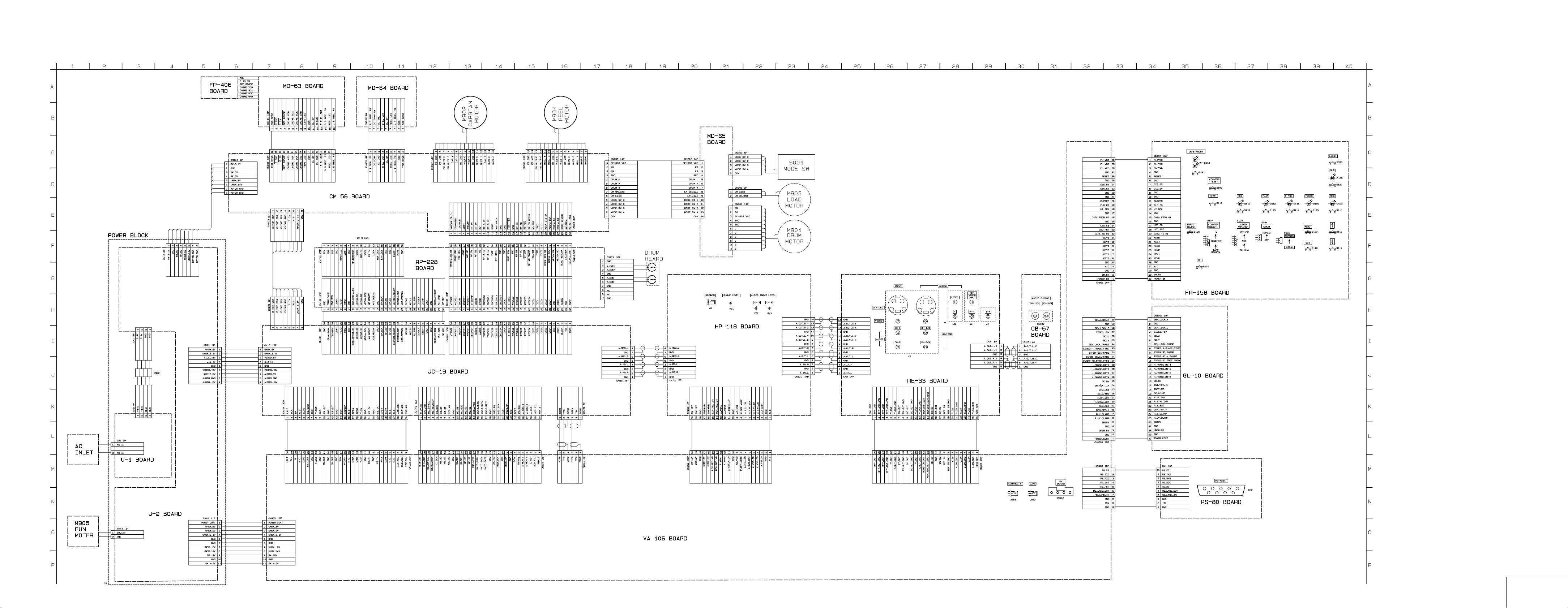
PRINTED WIRING BOARDS AND SCHEMATIC DIAGRAMS
4-1. FRAME SCHEMATIC DIAGRAM
DSR-40/40P
SECTION 4
4-1
4-2 4-3
FRAME
4-4
Page 28
DSR-40/40P
4-2. PRINTED WIRING BOARDS AND SCHEMATIC DIAGRAMS
THIS NOTE IS COMMON FOR PRINTED WIRING
BOARDS AND SCHEMATIC DIAGRAMS.
(In addition to this, the necessary note is printed
in each block)
For printed wiring boards:
• b : Pattern from the side which enables seeing.
(The other layers’ pattern are not indicated)
• Circled numbers refer to waveforms.
• Through hole is omitted.
• There are few cases that the part printed on diagram isn’t
mounted in this model.
• Chip parts.
Transistor Diode
5
5246
31
654
123
10
W unless otherwise noted.
22U
TA A
C
EB
For schematic Diagram:
• All capacitors are in µF unless otherwise noted. pF : µµF
50V or less are not indicated except for electrolytics and
tantalums.
• Chip resistors are 1/
kΩ : 1000Ω, MΩ : 1000kΩ.
• Caution when replacing chip parts.
New parts must be attached after removal of chip.
Be careful not to heat the minus side of tantalum capacitor,
because it is damaged by the heat.
• Some chip part will be indicated as follows.
Example C 541
21
21
21321321
345
123
L 452
10UH
2520
3
RP-228 BOARD (SIDE A)
CN101 A-2
CN102 A-4
CN771 B-6
CN775 A-5
D772 A-1
D774 B-5
D775 C-5
IC770 C-1
IC771 D-3
IC772 B-1
IC775 B-3
IC777 C-5
Q105 C-2
Q109 B-3
Q774 A-1
Q775 A-1
Q776 B-2
Q777 B-2
Q779 A-3
Q784 B-3
RP-228
1
A
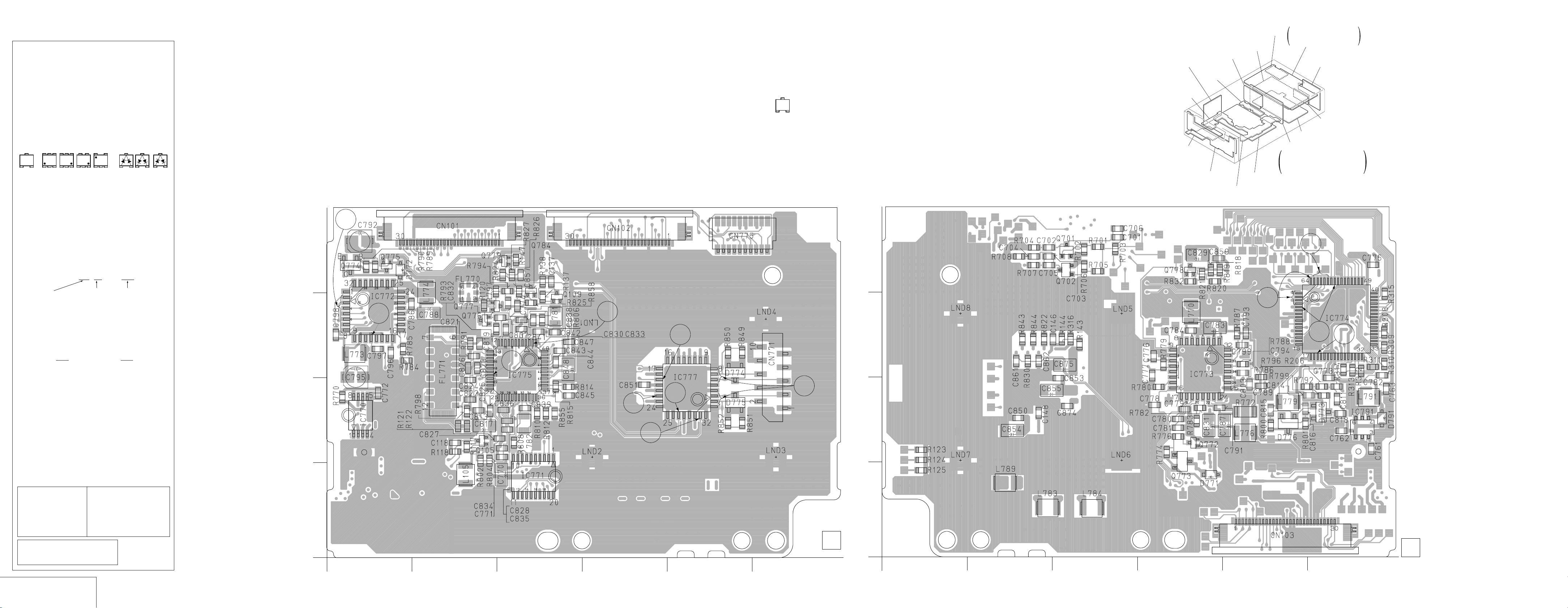
RP-228 (REC/PB AMP) PRINTED WIRING BOARD
– Ref. No.: RP-228 board; 7,000 series –
BOARD (SIDE A)
• For Printed Wiring Board.
• RP-228 board is six-layer print board. However, the patterns
of layers 2 to 5 have not been included in the diagram.
• There are few cases that the part isn't mounted in this model
is printed on this diagram.
• Chip transistor
C
EB
RP-228
A
BOARD (SIDE B)
GL-10
(SYNC GENERATOR)
MD-65
(TAPE DETECT)
MD-63
(TAPE DETECT)
HP-118
(AUDIO)
FR-158
(DISPLAY CONTROL)
RP-228
(REC/PB AMP)
MD-64
(TAPE DETECT)
RS-80
(RS-422A IF)
U-2
(POWER 2)
CM-56
(SERVO, SYSTEM CONTROL)
VA-106
IF, VIDEO IN/OUT, UVIC,
DV IN/OUT, MONITOR OUT,
HI MICOM, RS MICOM
U-1 (POWER 1)
JC-19
AD/DA CONVERTER, S1 AFC, U1,
D1, C1 SPCON, MODE, DV IN/OUT,
AUDIO CORE, DIGITAL AUDIO,
AUDIO D/A, A/D CONVERTER
13
RE-33
(V/A IN/OUT)
CB-67 (AUDIO OUT)
RP-228 BOARD
(SIDE B)
CN103 D-5
D771 D-4
D773 C-6
IC773 B-4
IC774 B-6
Q701 A-3
Q702 A-3
Q772 C-4
Q773 D-4
Q778 A-4
Kinds of Temperature External
capacitor characteristics dimensions (mm)
• Constants of resistors, capasitors, ICs and etc with XX indicate that they are not used. In such cases, the unused circuits may be indicated.
• Parts with ★ differ according to the model/destination. Refer to the mount table for each function.
• All variable and adjustable resistors have characteristic curve
B, unless otherwise noted.
• Signal name
XEDIT → EDIT PB/XREC → PB/REC
• 2 : nonflammable resistor.
• 1 : fusible resistor.
• C : panel designation.
• A : B+ Line.*
• B : B– Line.*
• J : IN/OUT direction of B line (+, –).*
• C : adjustment for repair.*
• Circled numbers refer to waveforms.*
Measuring conditions voltege and waveform:
• Voltages and waveforms are measured between the measurement points and graound when color bar signal
input.They are reference v alues and reference wav eforms.*
(VOM of DC 10 M Ω input impedance is used)
• Voltage values change depending upon input impedance
of VOM used.
* Indicated by the color red.
Note:
The components identified by mark ! or dotted
line with mark ! are critical for safety.
Replace only with part
number specified.
When indicating parts by reference
number, please include the board
name.
Note:
Les composants identifiés par
une marque ! sont critiques
pour la sécurité.
Ne les remplacer que par une
piéce portant le numéro
spécifié.
B
C
D
05
2
4
5
3
9
7
6
8
1-668-406-
12
123456
B
C
D
05
12
11
10
1-668-406-
12
123456
REC/PB AMP
RP-228
4-5 4-6 4-7 4-8
Page 29
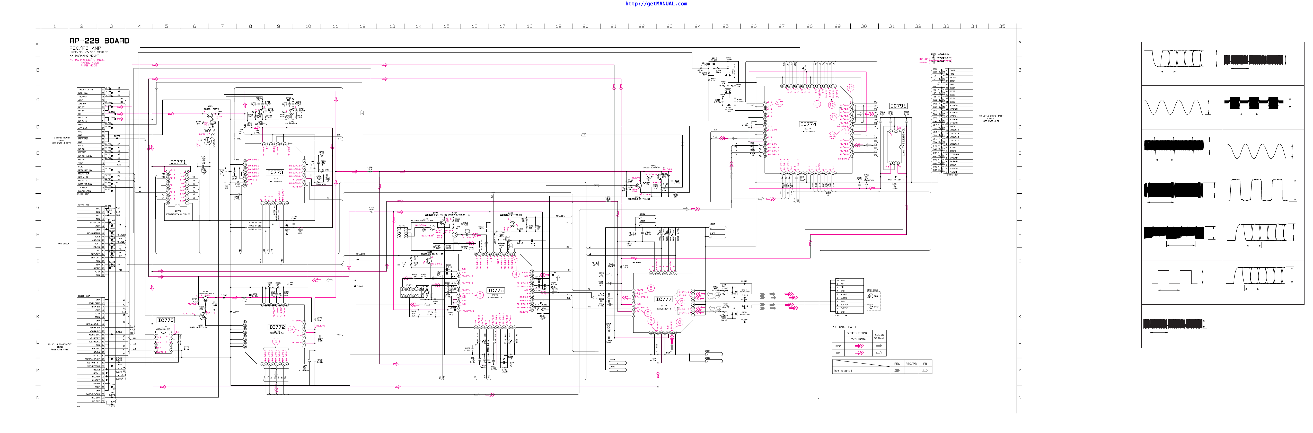
http://getMANUAL.com
RP-228 (REC/PB AMP) SCHEMATIC DIAGRAM
RP-228 BOARD
1
0.04 µsec
IC772 2 – 8 PB
2
41.8 MHz
IC772 !™ PB
3
3.4 Vp-p
2.3 Vp-p
1.6 Vp-p
DSR-40/40P
8
4.0 Vp-p
3.3 msec
IC777 #¡ REC
9
4.5 Vp-p
6.7 msec
IC777 2 3 6 7
0
4.3 Vp-p
4
5
6
7
3.3 msec
IC775 @º PB IC774 !ª REC/PB
!¡
0.5 Vp-p
3.3 msec
IC775 2 PB
!™
0.6 Vp-p
6.7 msec
IC777 !ª PB IC774 1 – 4, ^¢
!£
3.0 Vp-p
6.7 msec
IC777 @™ REC/PB IC774 %ª – ^£
0.25 µsec
0.25 µsec
41.8 MHz
3.6 Vp-p
8.38 MHz
IC774 5 REC/PB
IC774 %¶ PB
3.4 Vp-p
3.4 Vp-p
4-9 4-10 4-11
4-12
3.3 msec
IC777 @¶ REC
6.0 Vp-p
4-13
REC/PB AMP
RP-228
Page 30
DSR-40/40P
1-668-404-
05
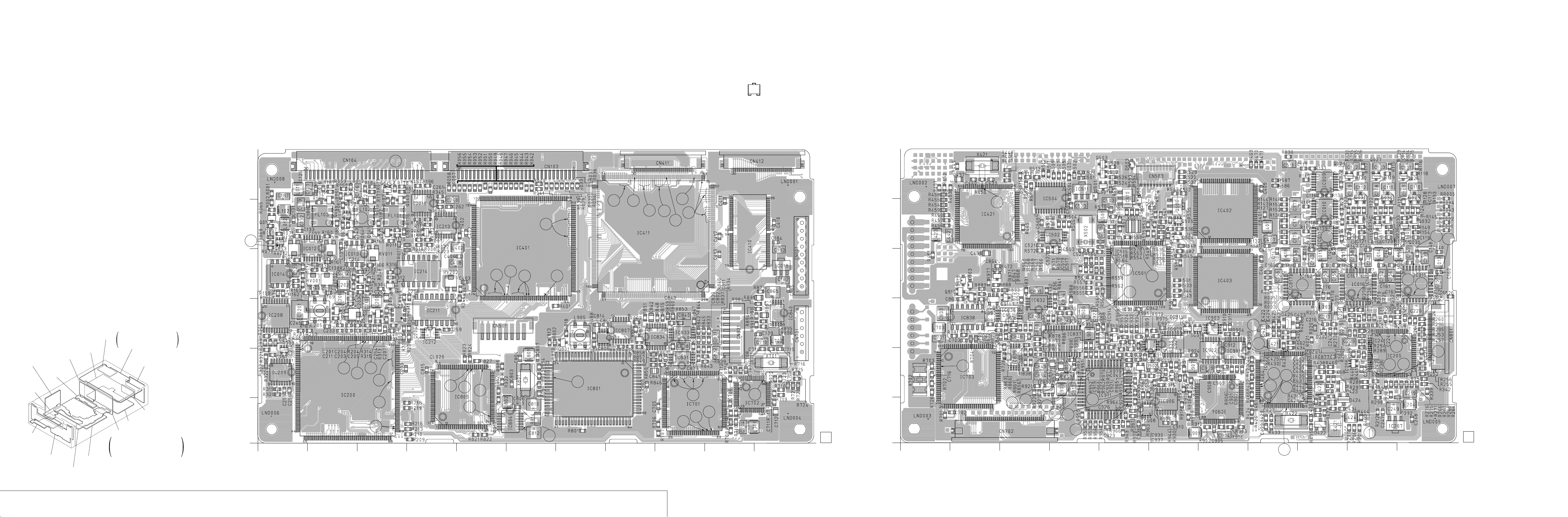
JC-19
BOARD (SIDE B)
A
B
C
D
E
F
1234567891011
21
41
49
43
42
64
60
59
58
57
63
62
4
5
6
7
8
10
9
17
18
19
20
21
36
34
40
39
37
38
61
35
JC-19 (AD/DA CONVERTER, S1 AFC, U1, D1, C1 SPCON, MODE, DV IN/OUT, AUDIO CORE,
JC-19 BOARD (SIDE A)
CN103 A-6
CN104 A-3
CN411 A-9
CN412 A-10
CN501 D-5
CN831 D-10
IC012 C-2
IC013 C-2
IC014 C-1
IC018 B-4
IC019 C-11
IC200 E-2
IC209 E-1
IC210 E-1
IC211 D-4
IC212 D-4
IC213 B-4
IC214 C-4
IC401 B-6
IC410 B-10
IC411 B-8
IC701 F-9
IC702 E-10
IC801 E-7
IC804 F-6
IC805 E-4
IC807 D-8
IC831 E-9
IC833 D-9
IC840 D-11
Q039 B-3
Q040 B-3
Q041 B-3
Q042 B-3
Q043 B-2
Q044 B-2
Q045 A-3
Q048 B-4
Q050 A-2
Q051 B-2
Q052 B-1
Q053 B-1
Q200 C-3
Q201 D-2
Q801 D-7
DIGITAL AUDIO, AUDIO D/A, A/D CONVERTER) PRINTED WIRING BOARD
– Ref. No.: JC-19 board; 5,000 series –
JC-19
BOARD (SIDE A)
A
B
3
1
33
32
31
2
26
C
22
23
24
25
51
50
GL-10
(SYNC GENERATOR)
MD-63
(TAPE DETECT)
HP-118
(AUDIO)
(DISPLAY CONTROL)
RP-228
(REC/PB AMP)
MD-65
(TAPE DETECT)
FR-158
MD-64
(TAPE DETECT)
RS-80
(RS-422A IF)
U-2
(POWER 2)
CM-56
(SERVO, SYSTEM CONTROL)
VA-106
IF, VIDEO IN/OUT, UVIC,
DV IN/OUT, MONITOR OUT,
HI MICOM, RS MICOM
RE-33
(V/A IN/OUT)
CB-67 (AUDIO OUT)
U-1 (POWER 1)
JC-19
AD/DA CONVERTER, S1 AFC, U1,
D1, C1 SPCON, MODE, DV IN/OUT,
AUDIO CORE, DIGITAL AUDIO,
AUDIO D/A, A/D CONVERTER
4-14 4-15
AD/DA CONVERTER, S1 AFC, U1, D1, C1 SPCON, MODE, DV IN/OUT, AUDIO CORE, DIGITAL AUDIO, AUDIO D/A, A/D CONVERTER
D
05
E
16
14
15
13
12
F
1234567891011
11
55
54
52
53
JC-19
30
29
28
44
27
47
45
46
4-16
• For Printed Wiring Board.
• JC-19 board is six-lay er print board. How ev er , the patterns of
layers 2 to 5 have not been included in the diagram.
• There are few cases that the part isn't mounted in this model
is printed on this diagram.
• Chip transistor
C
EB
48
1-668-404-
21
4-17 4-18
JC-19 BOARD (SIDE B)
CN101 B-1
CN503 A-6
CN701 D-1
D201 D-9
D421 D-8
D422 F-9
D423 E-9
D424 E-9
D425 D-8
D501 A-4
D503 A-5
D504 B-5
D901 E-6
D902 E-6
D903 C-2
D910 C-2
IC009 A-9
IC010 B-9
IC011 B-9
IC015 C-11
IC016 C-10
IC017 C-9
IC205 E-10
IC206 E-10
IC207 F-10
IC402 B-7
IC403 C-7
IC421 B-2
IC422 E-8
IC501 C-5
IC502 B-4
IC503 B-4
IC504 A-4
IC510 A-5
IC511 A-4
IC703 E-2
IC802 E-3
IC832 D-3
IC835 E-3
IC836 D-3
IC837 D-4
IC838 D-2
IC841 D-2
IC901 D-7
IC902 D-7
IC903 D-7
IC904 F-7
IC906 F-6
IC907 D-6
IC908 F-5
IC909 D-6
IC911 E-5
IC914 D-5
IC915 D-6
IC916 D-6
Q026 A-11
Q027 A-10
Q028 A-10
Q029 A-11
Q030 A-10
Q031 A-10
Q032 B-11
Q033 B-10
Q034 B-10
Q035 B-11
Q036 B-10
Q037 B-10
Q501 A-5
Q502 A-5
Q504 B-6
Q505 B-6
Q506 B-6
Q832 C-2
Q902 E-6
Q903 D-5
Q910 C-2
Q911 C-3
Page 31

JC-19 (AD/DA CONVERTER) SCHEMATIC DIAGRAM
JC-19 BOARD (1/10)
1
DSR-40/40P
6
0.54 Vp-p
H
Q045 E PB
27
0.54 Vp-p
H
Q051 2 PB
38
0.39 Vp-p
H
Q053 2 PB IC015 @¡ REC
4
2.0 Vp-p
9
H
IC016 @¡ REC
0.15 µsec
IC016 1 – 8 REC
H
0.9 Vp-p
3.6 Vp-p
0.8 Vp-p
3.6 Vp-p
H
IC017 @¡ REC
50
3.6 Vp-p
0.15 µsec
IC017 1 – 8 REC IC015 – IC017 !™ REC/PB
0.15 µsec
IC015 1 – 8 REC
3.4 Vp-p
13.5 MHz
4-19
4-20 4-21 4-22
AD/DA CONVERTER
JC-19 (1/10)
Page 32

DSR-40/40P
JC-19 BOARD (2/10)
!¡
JC-19 (S1 AFC) SCHEMATIC DIAGRAM • See page 4-14 for JC-19 printed wiring board.
!¶
3.8 Vp-p
13.5 MHz
IC200 (º (¡ REC/PB
!™ !•
3.4 Vp-p
0.15 µsec
IC200 `⁄⁄⁄ – `⁄⁄° REC/PB
!£ !ª
3.4 Vp-p
0.15 µsec
IC200 `⁄¤¤ – `⁄¤· REC/PB IC205 !• @º REC/PB
!¢ @º
1.2 Vp-p
H
IC200 `⁄‹· PB
!∞ @¡
0.8 Vp-p
H
IC205 7 REC
3.2 Vp-p
13.5 MHz
IC205 !∞ REC/PB
3.0 Vp-p
H
3.0 Vp-p
H
IC205 @• REC/PB
!§
0.39 Vp-p
H
IC200 `⁄›fi PB IC205 $¡ REC/PB
0.54 Vp-p
H
IC200 `⁄›fl PB
13.5 MHz
3.2 Vp-p
S1 AFC
JC-19 (2/10)
4-24 4-25 4-26 4-27 4-28
Page 33

JC-19 (U1) SCHEMATIC DIAGRAM • See page 4-14 for JC-19 printed wiring board.
DSR-40/40P
JC-19 BOARD (3/10)
@™
3.4 Vp-p
0.12 µsec
IC401 5 – !¡ !£ REC/PB
@£
3.6 Vp-p
13.5 MHz
IC401 !¢ REC/PB
@¢
0.12 µsec
IC401 !¶ – @™ @¢ @∞ REC/PB
@∞
18.16 MHz
IC401 #£ REC/PB
@§
0.12 µsec
IC401 ^• – &¶ &ª – *¢ REC/PB
3.4 Vp-p
3.2 Vp-p
2.4 Vp-p
4-29
4-30 4-31 4-32
U1
JC-19 (3/10)
Page 34

DSR-40/40P
JC-19 (D1) SCHEMATIC DIAGRAM • See page 4-14 for JC-19 printed wiring board.
JC-19 BOARD (4/10)
@¶
3.2 Vp-p
0.1 µsec
IC411 #¢ – $¡, $¢ – %º, %¢ REC/PB
@•
3.0 Vp-p
6.6 msec
IC411 %• REC/PB
@ª
#º
#¡
#™
#£
3.6 Vp-p
8.38 MHz
IC411 &™ REC
3.2 Vp-p
0.25 µsec
IC411 &¢ – &¶ REC
3.6 Vp-p
0.25 µsec
IC411 *¡ – *∞ PB
3.6 Vp-p
8.37 MHz
IC411 *• PB
D1
JC-19 (4/10)
0.25 µsec
IC411 (¡ – (∞ PB
4-33
3.4 Vp-p
4-34 4-35 4-36
Page 35

JC-19 (C1 SPCON) SCHEMATIC DIAGRAM • See page 4-14 for JC-19 printed wiring board.
DSR-40/40P
JC-19 BOARD (5/10)
#¢
3.4 Vp-p
13.5 MHz
IC422 2 3 @• REC/PB
#∞
3.4 Vp-p
27 MHz
IC422 !™ REC/PB
#§
3.2 Vp-p
#¶
#•
#ª
$º
13.5 MHz
IC422 @∞ REC/PB
3.2 Vp-p
18.1 MHz
IC422 $• $ª REC/PB
2.5 Vp-p
36.3 MHz
IC422 %∞ REC/PB
2.9 Vp-p
33 msec
IC422 &£ REC/PB
4-37
6.6 msec
IC422 &¢ REC/PB
$¡
20 MHz
IC421 $º REC/PB
4-38 4-39 4-40
2.8 Vp-p
2.8 Vp-p
C1 SPCON
JC-19 (5/10)
Page 36

DSR-40/40P
JC-19 BOARD (6/10)
$™
JC-19 (MODE) SCHEMATIC DIAGRAM • See page 4-14 for JC-19 printed wiring board.
2.8 Vp-p
20 MHz
$£
IC501 $º REC/PB
2.5 Vp-p
32.768 kHz
IC501 %™ REC/PB
MODE
JC-19 (6/10)
4-41 4-42 4-43 4-44
Page 37

JC-19 (DV IN/OUT) SCHEMATIC DIAGRAM • See page 4-14 for JC-19 printed wiring board.
DSR-40/40P
JC-19 BOARD (7/10)
$¢
2.9 Vp-p
33 msec
IC701 $£ REC/PB
$∞
2.9 Vp-p
6.6 msec
IC701 $∞ REC/PB
$§
$¶
$•
$ª
18.16 MHz
IC701 $¶ REC/PB
100 nsec
*™ – *∞ *¶ – (º (™ – (∞
IC701
(¶ – `⁄‚‚ REC/PB
24.57 MHz
IC702 #¶ REC/PB
6 MHz
IC703 8 REC/PB
3.0 Vp-p
3.2 Vp-p
2.9 Vp-p
2.9 Vp-p
4-45
4-46 4-47 4-48
DV IN/OUT
JC-19 (7/10)
Page 38

DSR-40/40P
DSR-40/40P
JC-19 (AUDIO CORE) SCHEMATIC DIAGRAM • See page 4-14 for JC-19 printed wiring board.
JC-19 BOARD (8/10)
%º
0.9 Vp-p
49.152 MHz
IC801 @ª REC/PB
%¡
4.5 Vp-p
3 MHz
IC804 8 REC/PB
%™
%£
%¢
%∞
3.6 Vp-p
12.3 MHz
IC805 @• REC/PB
2.8 Vp-p
18.16 MHz
IC805 %£ REC/PB
3.1 Vp-p
1.1 msec
IC805 %• REC
3.1 Vp-p
1.1 msec
IC805 ^º PB
AUDIO CORE
JC-19 (8/10)
4-50 4-51 4-52
Page 39

JC-19 (DIGITAL AUDIO) SCHEMATIC DIAGRAM • See page 4-14 for JC-19 printed wiring board.
DSR-40/40P
JC-19 BOARD (9/10)
%¶
3.1 Vp-p
33 msec
IC911 2 PB
%•
2.3 Vp-p
24.57 MHz
IC911 @¢ REC/PB
%ª
^º
3.4 Vp-p
6.1 MHz
IC911 @• REC/PB
3.4 Vp-p
12.3 MHz
IC911 #º REC/PB
4-53
4-54 4-55 4-56
DIGITAL AUDIO
JC-19 (9/10)
Page 40

DSR-40/40P
DSR-40/40P
JC-19 (AUDIO D/A, A/D CONVERTER) SCHEMATIC DIAGRAM • See page 4-14 for JC-19 printed wiring board.
JC-19 BOARD (10/10)
^¡
3.0 Vp-p
48 kHz
IC837 !¡ REC/PB
^™
3.4 Vp-p
3 MHz
^£
^¢
IC837 !™ REC/PB
3.6 Vp-p
1 µsec
IC837 !£ PB
3.4 Vp-p
12.3 MHz
IC837 !∞ PB
AUDIO D/A, A/D CONVERTER
JC-19 (10/10)
4-58
4-59
4-60
Page 41

RE-33 (V/A IN/OUT), CB-67 (AUDIO OUT) PRINTED WIRING BOARDS AND SCHEMATIC DIAGRAM
– Ref. No.: RE-33 board; 6,000/CB-67 board; 6,000 series –
DSR-40/40P
• For Printed Wiring Board.
• There are cases that the part isn't mounted in this model is
printed on this diagram.
RE-33
A
B
C
05
BOARD (SIDE A)
A
K
K
A
A
K
K
A
RE-33
BOARD (SIDE B)
REF VIDEO
INPUT
OUTPUT
INPUT
A
KK
A
B-Y
A
KK
B
A
K
K
A
K
A
A
K
1-673-140-
11
1234
C
05
1234
A
R-Y
KK
VIDEO
S VIDEO
Y
KK
A
VIDEO
A
MONITOR
A
CGY
G
A
A
KK
KK
KK
A
K
K
CH-1/3
A
AUDIO
A
CH-2/3
K
K
A
A
K
A
K
K
A
CGY
G
KK
KK
A
KK
S VIDEO
A
VIDEO
A
K
CH-1
AUDIO
CH-2
1-673-140-
11
RE-33 BOARD (SIDE A)
CN2 B-1
CN3 C-1
D19 C-1
D20 C-1
D21 B-1
D22 B-1
D23 A-1
D24 A-1
D25 A-1
D26 A-1
IC1 B-1
GL-10
(SYNC GENERATOR)
MD-65
(TAPE DETECT)
MD-63
(TAPE DETECT)
HP-118
(AUDIO)
FR-158
(DISPLAY CONTROL)
RP-228
(REC/PB AMP)
MD-64
(TAPE DETECT)
RS-80
(RS-422A IF)
U-2
VA-106
IF, VIDEO IN/OUT, UVIC,
DV IN/OUT, MONITOR OUT,
HI MICOM, RS MICOM
(POWER 2)
U-1 (POWER 1)
JC-19
AD/DA CONVERTER, S1 AFC, U1,
D1, C1 SPCON, MODE, DV IN/OUT,
AUDIO CORE, DIGITAL AUDIO,
CM-56
AUDIO D/A, A/D CONVERTER
(SERVO, SYSTEM CONTROL)
RE-33
(V/A IN/OUT)
CB-67 (AUDIO OUT)
4-61 4-62 4-63 4-64
CB-67
05
BOARD (SIDE A)
1-673-141-
11
CB-67
05
BOARD (SIDE B)
AUDIO CH-2/4
1
21
3
AUDIO CH-1/3OUTPUT
3
1-673-141-
RE-33 BOARD (SIDE B)
CN1 A-3
D1 C-3
D2 C-3
D3 C-3
D4 C-4
D5 B-4
D6 B-4
D7 B-4
D8 C-3
D9 B-3
D10 C-3
D11 C-3
D12 C-3
D13 B-3
D14 B-3
D15 B-1
D16 B-1
D17 B-2
D18 A-2
2
11
4-65
V/A IN/OUT, AUDIO OUT
RE-33 CB-67
Page 42

DSR-40/40P
VA-106 (IF, VIDEO IN/OUT, UVIC, DV IN/OUT, MONITOR OUT, HI MICOM, RS MICOM) PRINTED WIRING BOARD
– Ref. No.: VA-106 board; 10,000 series –
VA-106 BOARD (SIDE A)
CN0001 D-3
CN101 E-5
CN102 E-6
CN401 B-7
CN601 A-2
CN602 A-2
CN851 E-3
CN852 A-1
CN855 E-7
CN856 E-1
D201 C-7
D401 B-5
D402 B-5
D403 C-4
D651 B-3
D851 A-4
D852 A-4
D854 D-1
D858 C-1
D860 E-2
IC101 E-5
IC104 E-4
IC105 E-4
IC106 E-5
IC202 B-7
IC219 D-7
IC401 B-5
IC409 C-6
IC410 B-5
IC411 D-4
IC413 D-5
IC414 D-5
IC416 D-4
IC417 B-6
IC418 C-6
IC421 C-6
IC426 C-3
IC429 D-5
IC430 B-5
IC854 E-1
IC855 A-2
IC857 B-4
IC860 A-3
IC861 E-2
IC862 E-7
IC1115 D-3
IC1116 D-3
Q0004 C-2
Q101 E-5
Q102 E-5
Q103 E-5
Q202 C-7
Q203 B-7
Q205 B-7
Q206 C-6
Q207 C-6
Q208 B-7
Q209 C-6
Q211 D-6
Q215 B-6
Q218 B-8
Q220 C-8
Q225 C-8
Q228 D-6
Q421 C-5
Q422 C-5
Q423 C-5
Q425 B-5
Q427 B-5
Q607 E-4
Q613 D-4
Q653 B-2
Q654 B-2
Q851 D-2
Q853 D-1
Q854 E-7
VA-106 BOARD (SIDE A)
A
9
10
B
C
A
K
D
E
58
2
1
59
IN/OUT
1
2
29
DV
3
4
KA
LANC
3
4
CONTROL S
A
K
K
K
A
1
3
4
13
5
4
38
5
1
1
5
AK
A
1
3
VA-106
IF, VIDEO IN/OUT, UVIC,
DV IN/OUT, MONITOR OUT,
HI MICOM, RS MICOM
RE-33
(V/A IN/OUT)
GL-10
(SYNC GENERATOR)
RP-228
(REC/PB AMP)
RS-80
(RS-422A IF)
U-2
(POWER 2)
MD-65
(TAPE DETECT)
MD-63
(TAPE DETECT)
VA-106 BOARD (SIDE B)
CB-67 (AUDIO OUT)
U-1 (POWER 1)
HP-118
(AUDIO)
JC-19
AD/DA CONVERTER, S1 AFC, U1,
D1, C1 SPCON, MODE, DV IN/OUT,
A
AUDIO CORE, DIGITAL AUDIO,
(DISPLAY CONTROL)
FR-158
2
25
4
3
1
5
40
3
4
1
5
12 7
K
42
1
2
1
34
6
2
3
CM-56
(SERVO, SYSTEM CONTROL)
MD-64
(TAPE DETECT)
AUDIO D/A, A/D CONVERTER
B
9
1
127
1
30
31
5
28
32
27
1
5
4
5
4
3
4
1
3
4
3
5
1
33
K
A
1
12
6
7
3
1
4
5
6
1
5
C
D
5
1
1
3
5
4
6
4
18
3
E
• For Printed Wiring Board.
• V A-106 board is 4-la y er print board. Ho wev er, the patterns of
layers 2 to 3 have not been included in the diagram.
• There are few cases that the part isn't mounted in this model
is printed on this diagram.
• Chip transistor
5
C
5246
EB
31
654
123
8
64
65
41
40
6
14
A
12
7
80
1
K
11
13
10
5
4
25
24
17
16
15
5
4
5
4
3
1
3
A
K
4
5
1
3
1
3
4
5
1
39
VA-106 BOARD (SIDE B)
D202 C-1
D404 D-3
D405 D-3
D406 D-4
D407 B-4
D408 B-3
D855 C-8
D856 C-8
D857 C-8
D859 E-1
D862 E-6
K
A
1
3
5
4
K
K
A
56
K
41
K
A
A
K
53
52
54
57
55
A
43
45
26
48
35
37
36
47
25
34
5
1
6
13
4
3
7
9
10
12
A
A
K
K
60
44
46
7
6
3
4
1
5
1
12
7
6
1
12
7
6
1
12
29
AK
K
A
D863 A-5
IC0001 C-7
IC0002 C-6
IC102 E-5
IC103 E-5
IC201 B-1
IC203 B-1
IC204 D-2
IC205 B-1
IC206 E-2
IC207 C-1
IC208 C-1
IC209 E-2
IC210 C-1
IC211 B-2
IC212 D-2
IC213 D-2
IC 214 E-2
IC215 D-1
IC216 D-1
IC217 C-1
IC218 E-2
IC220 D-2
IC221 D-2
IC222 D-1
IC402 E-3
IC403 E-4
IC404 E-3
IC405 E-3
IC406 D-4
IC407 D-5
IC408 B-3
IC412 D-3
IC415 B-3
IC419 B-3
IC420 C-5
IC422 C-5
IC423 C-4
IC424 D-5
IC425 C-5
IC427 D-3
IC428 D-3
IC602 E-5
IC651 B-6
IC652 B-6
IC653 B-7
IC654 B-7
IC851 A-5
IC853 A-5
IC856 C-8
IC858 D-8
IC859 C-8
IC1105 C-6
IC1110 D-6
IC1114 C-6
Q0001 C-7
Q0002 C-7
Q0003 C-6
Q201 C-2
Q204 D-2
Q210 C-3
Q212 C-3
Q213 C-3
Q214 B-3
Q216 C-1
Q217 D-2
Q219 E-2
Q221 C-1
Q222 C-2
Q223 D-1
Q224 D-3
Q226 D-3
Q227 D-2
Q229 D-1
Q230 D-3
Q231 D-1
Q232 E-2
Q233 D-1
Q234 B-1
Q235 B-2
Q236 B-1
Q401 E-3
Q402 E-3
Q403 E-4
Q404 D-6
Q405 D-6
Q406 D-3
Q407 D-3
Q408 D-4
Q409 D-3
Q410 D-3
Q411 D-4
Q412 D-5
Q413 D-3
Q414 D-3
Q415 D-4
Q416 D-5
Q417 D-4
Q418 D-4
Q419 D-4
Q420 D-5
Q426 B-3
Q428 C-6
Q429 C-6
Q430 C-5
Q431 E-3
Q432 D-3
Q433 D-4
Q601 D-4
Q602 D-4
Q604 D-4
Q605 E-4
Q606 E-4
Q651 B-6
Q652 A-6
Q852 C-8
Q855 E-6
24
46
31
1
51
8
9
16
17
50
32
1
25
49
24
3
6
4
K
A
BCE
23
29
1
05
12345678
19
1
29
4-66
IF, VIDEO IN/OUT, UVIC, DV IN/OUT, MONITOR OUT, HI MICOM, RS MICOM
VA-106
1
29
1
1-673-138-
11
05
12345678
19
20
21
22
4-67 4-68 4-69 4-70
1-673-138-
11
Page 43

VA-106 (IF) SCHEMATIC DIAGRAM
DSR-40/40P
4-71
4-72
IF
VA-106 (1/7)
Page 44

DSR-40/40P
VA-106 (VIDEO IN) SCHEMATIC DIAGRAM • See page 4-66 for VA-106 printed wiring board.
VIDEO IN
VA-106 (2/7)
4-75
4-76 4-77 4-78
Page 45

VA-106 BOARD (2/7)
1
8
!∞
2
3
4
5
H
Q202 B REC
H
IC202 1 REC
H
Q203 E REC
H
IC211 @∞ REC
1 Vp-p
1 Vp-p
640 mVp-p
1.5 Vp-p
9
!º
!¡
!™
H
IC203 7 REC
H
IC205 7 REC
H
IC213 @∞ REC
H
IC213 5 REC
1 Vp-p
630 mVp-p
500 mVp-p
260 mVp-p
860 mVp-p
DSR-40: 3.58 MHz
DSR-40P: 4.43 MHz
Q231 E REC/PB
!§
1 Vp-p
H
IC204 6 REC
!¶
760 mVp-p
H
IC212 6 REC
!•
2.4 Vp-p
H
IC215 1 REC
!ª
H
IC211 #¡ REC
6
H
IC211 #ª REC
7
DSR-40: 14.32 MHz
DSR-40P: 17.73 MHz
IC211 !¡ REC/PB
1.4 Vp-p
960 mVp-p
2.8 Vp-p
DSR-40: 14.32 MHz
DSR-40P: 17.73 MHz
IC213 !º REC/PB
!£
H
IC213 @º REC
!¢
H
IC213 !ª REC
1.7 Vp-p
1.3 Vp-p
1 Vp-p
1.1 Vp-p
H
IC209 1 REC
@º
1.1 Vp-p
H
IC218 1 REC
4-79
Page 46

VA-106 BOARD (3/7)
@¡
500 mVp-p
#¡
700 mVp-p
$º
1.4 Vp-p
@™
@£
@¢
@∞
H
H
H
Q401 B PB
Q402 B PB
Q403 B PB
H
Q404 5 PB
540 mVp-p
390 mVp-p
1.2 Vp-p
680 mVp-p
#£
#™
#¢
#∞
H
Q423 6 PB
H
IC418 1 PB
H
IC421 1 PB
H
IC422 @¢ PB
1 Vp-p
1 Vp-p
450 mVp-p
450 mVp-p
$™
$¡
$£
$¢
H
IC410 !£ PB
H
IC415 !£ REC/PB
H
IC417 !£ REC/PB
H
IC419 !£ REC/PB
2.2 Vp-p
1.3 Vp-p
2.2 Vp-p
680 mVp-p
@§
@•
@ª
#º
@¶
H
Q412 3 PB
H
Q416 5 PB
H
IC409 2 PB
H
IC409 !§ PB
H
IC412 1 PB
1.3 Vp-p
470 mVp-p
670 mVp-p
1.4 Vp-p
700 mVp-p
#§
#¶
#ª
#•
H
IC422 1 PB
IC422 3 PB
H
IC422 !• PB
H
IC426 1 PB
H
IC408 !£ PB
500 kHz
IC423 !º REC/PB
$∞
1.1 Vp-p
H
$§
840 mVp-p
$¶
680 mVp-p
$•
1.4 Vp-p
DSR-40: 14.32 MHz
DSR-40P: 17.73 MHz
H
IC423 9 REC/PB
V
IC423 5 REC/PB
H
IC425 @∞ REC/PB
IC425 8 REC/PB
4.3 Vp-p
4 Vp-p
2.2 Vp-p
4.6 Vp-p
H
Q422 6 PB
4-80
Page 47

VA-106 (VIDEO OUT) SCHEMATIC DIAGRAM • See page 4-66 for VA-106 printed wiring board.
DSR-40/40P
4-81 4-82
4-83 4-84
VIDEO OUT
VA-106 (3/7)
Page 48

DSR-40/40P
VA-106 (UVIC, DV IN/OUT) SCHEMATIC DIAGRAM • See pag e 4-66 for VA-106 printed wiring board.
VA-106 BOARD (4/7)
$ª
3.3 Vp-p
DSR-40: 3.58 MHz
DSR-40P: 4.43 MHz
IC602 #¡ REC/PB
%º
2.1 Vp-p
%¡
H
IC602 !• REC/PB
960 mVp-p
H
IC602 !¶ REC/PB
UVIC, DV IN/OUT
4-85 4-86 4-87 4-88
VA-106 (4/7)
Page 49

VA-106 (MONITOR OUT) SCHEMATIC DIAGRAM • See page 4-66 for VA-106 printed wiring board.
DSR-40/40P
VA-106 BOARD (5/7)
%™
2.2 Vp-p
H
IC651 @∞ REC/PB
%£
4.6 Vp-p
DSR-40: 14.32 MHz
DSR-40P: 17.73 MHz
IC651 8 REC/PB
%¢
%∞
%§
1 Vp-p
H
IC652 2 REC/PB
4 Vp-p
V
IC652 5 REC/PB
680 mVp-p
500 kHz
IC652 !º REC/PB
%¶
4.3 Vp-p
H
IC652 9 REC/PB
4-89
4-90
4-91
MONITOR OUT
VA-106 (5/7)
Page 50

DSR-40/40P
VA-106 (HI CON) SCHEMATIC DIAGRAM • See page 4-66 for VA-106 printed wiring board.
HI CON
VA-106 (6/7)
4-92
4-93
4-94
Page 51

VA-106 BOARD (6/7)
%•
20 MHz
IC854 $™ REC/PB
%ª
DSR-40/40P
VA-106 (SG SELECT, EVR) SCHEMATIC DIAGRAM • See page 4-66 for VA-106 printed wiring board.
6.5 Vp-p
3.1 Vp-p
^º
32.798 kHz
IC854 %¢ REC/PB
560 mVp-p
32.798 kHz
IC858 2 REC/PB
4-95 4-96
SG SELECT, EVR
VA-106 (7/7)
Page 52

DSR-40/40P
RS-80 (RS-422A IF) PRINTED WIRING BOARD
– Ref. No.: RS-80 board; 3,000 series –
RS-80
BOARD (SIDE A)
A
B
• For Printed Wiring Board.
• There are fe w cases that the part isn't mounted in this model
is printed on this diagram.
REMOTE
RS-80
BOARD (SIDE B)
1
RS-422A
9
5
6
1
A
K
2
A
K
A
K
K
K
K
A
1-673-143-
B
11
A
A
K
A
1-673-143-
KAK
11
05
RS-80 BOARD (SIDE A)
CN1 B-1
D5 B-2
D6 B-2
D7 B-2
IC3 A-1
123
RS-80
(RS-422A IF)
U-2
(POWER 2)
GL-10
(SYNC GENERATOR)
MD-65
(TAPE DETECT)
MD-63
(TAPE DETECT)
RP-228
(REC/PB AMP)
05
VA-106
IF, VIDEO IN/OUT, UVIC,
DV IN/OUT, MONITOR OUT,
HI MICOM, RS MICOM
RE-33
(V/A IN/OUT)
123
RS-80 BOARD (SIDE B)
CN 2 A-2
D 1 A-2
D 2 A-3
D 3 A-2
D 4 A-2
IC 1 A-1
IC 2 A-2
RS-422A IF
RS-80
CB-67 (AUDIO OUT)
U-1 (POWER 1)
HP-118
(AUDIO)
FR-158
(DISPLAY CONTROL)
CM-56
(SERVO, SYSTEM CONTROL)
MD-64
(TAPE DETECT)
JC-19
AD/DA CONVERTER, S1 AFC, U1,
D1, C1 SPCON, MODE, DV IN/OUT,
AUDIO CORE, DIGITAL AUDIO,
AUDIO D/A, A/D CONVERTER
4-97 4-98
Page 53

RS-80 (RS-422A IF) SCHEMATIC DIAGRAM
DSR-40/40P
RS-80 BOARD
1
4.7 Vp-p
614 kHz
2
IC2 3 REC/PB
4.3 Vp-p
8 MHz
IC1 7 REC/PB
4-99
4-100
4-101
RS-422A IF
RS-80
Page 54

DSR-40/40P
• For Printed Wiring Board.
• There are few cases that the part isn't mounted in this model is printed
on this diagram.
• Chip transistor
C
EB
VA-106
IF, VIDEO IN/OUT, UVIC,
DV IN/OUT, MONITOR OUT,
HI MICOM, RS MICOM
RE-33
(V/A IN/OUT)
CB-67 (AUDIO OUT)
U-1 (POWER 1)
JC-19
AD/DA CONVERTER, S1 AFC, U1,
D1, C1 SPCON, MODE, DV IN/OUT,
AUDIO CORE, DIGITAL AUDIO,
AUDIO D/A, A/D CONVERTER
GL-10
(SYNC GENERATOR)
MD-65
(TAPE DETECT)
MD-63
(TAPE DETECT)
HP-118
(AUDIO)
FR-158
(DISPLAY CONTROL)
RP-228
(REC/PB AMP)
MD-64
(TAPE DETECT)
RS-80
(RS-422A IF)
U-2
(POWER 2)
CM-56
(SERVO, SYSTEM CONTROL)
FR-158 BOARD (SIDE A)
D101 A-1
D102 C-4
D108 B-7
D109 B-7
D110 B-7
D111 B-6
D112 B-6
D113 A-1
D114 A-1
D117 B-6
Q101 A-1
FR-158 BOARD (SIDE B)
CN104 A-5
D115 B-3
D116 A-5
IC103 B-5
IC104 B-3
Q103 B-7
Q104 B-7
Q105 B-7
Q106 B-6
Q107 B-6
Q110 B-6
FR-158 (DISPLAY CONTROL) PRINTED WIRING BOARD
– Ref. No.: FR-158 board; 3,000 series –
FR-158
BOARD (SIDE A)
ON/STANDBY
K
A
A
A
K
POWER
SW
K
K
A
B
C
05
12345678
FR-158 BOARD (SIDE B)
A
INPUT
SELECT
A
K
COUNTER
RESET
COUNTER
CL
K
TC
TAPE
REMAIN
A
STOP
p
S107
COUNTER
SELECT
AUDIO
MONITOR
REW
0
REW
CH-1/2
MIX
CH
3/4
PLAY
PLAY
(
TIMER
REPEAT
OFF
EJECT
DUP
FF
)
LOCAL/
REMOTE
REC
PAUSE
FF
REMOTE
LOCAL
DUP
PAUSE
P
MENU
SET
UP
DOUN
1-673-142-
REC
r
11
DISPLAY CONTROL
FR-158
4-102
B
K
A
C
1-673-142-
11
05
12345678
4-103
4-104
Page 55

FR-158 (DISPLAY CONTROL) SCHEMATIC DIAGRAM
DSR-40/40P
4-105
4-106
4-107
DISPLAY CONTROL
FR-158
Page 56

DSR-40/40P
A
B
C
123
1-673-139-
GL-10
BOARD (SIDE B)
11
1
9
8
16
17
24
25
32
5
1
3
4
K
A
K
A
S
D
G
5
4
1
3
1
9
8
16
17
24
25
32
05
6
7
13
5
12
11
10
4
3
2
1
• For Printed Wiring Board.
• GL-10 board is 4-layer print board. However, the patterns of layers
2 to 3 have not been included in the diagram.
• There are few cases that the par t isn't mounted in this model is
printed on this diagram.
• Chip transistor
5
C
5246
EB
31
GL-10 BOARD (SIDE A)
D1102 C-1
IC1104 A-3
IC1105 A-3
IC1107 A-3
IC1108 A-3
IC1111 B-3
IC1112 B-3
IC1116 B-1
IC1118 B-2
IC1119 B-1
IC1121 A-2
IC1128 B-2
IC1132 B-3
IC1133 C-3
IC1134 B-1
IC1135 C-2
IC1136 B-1
IC1137 B-3
IC1138 C-2
IC1139 C-2
IC1140 B-1
IC1142 A-2
IC1143 A-2
IC1144 B-2
Q1104 C-2
Q1105 C-2
Q1106 C-2
GL-10 (SYNC GENERATOR) PRINTED WIRING BOARD
– Ref. No.: GL-10 board; 20,000 series –
GL-10
BOARD (SIDE A)
A
6
GL-10 BOARD (SIDE B)
CN1001 C-2
D1101 B-3
D1103 B-2
IC1101 B-1
IC1102 B-2
IC1103 A-3
IC1106 B-2
IC1109 B-2
IC1113 B-2
IC1115 B-3
IC1117 B-3
IC1120 C-3
IC1122 A-2
IC1123 C-3
IC1124 A-2
IC1125 A-2
IC1126 B-3
IC1127 A-3
IC1129 B-3
IC1130 A-2
IC1131 B-3
IC1141 B-2
Q1101 C-1
Q1102 C-1
Q1103 A-2
SYNC GENERATOR
GL-10
1
5
B
6
1
5
A
K
3
15
C
1
4
5
5
4
1
3
14
05
123
4-108 4-109 4-110
9
8
GL-10
(SYNC GENERATOR)
MD-63
(TAPE DETECT)
1-673-139-
MD-65
(TAPE DETECT)
HP-118
(AUDIO)
FR-158
(DISPLAY CONTROL)
11
RP-228
(REC/PB AMP)
MD-64
(TAPE DETECT)
RS-80
(RS-422A IF)
U-2
(POWER 2)
CM-56
(SERVO, SYSTEM CONTROL)
VA-106
IF, VIDEO IN/OUT, UVIC,
DV IN/OUT, MONITOR OUT,
HI MICOM, RS MICOM
U-1 (POWER 1)
JC-19
AD/DA CONVERTER, S1 AFC, U1,
D1, C1 SPCON, MODE, DV IN/OUT,
AUDIO CORE, DIGITAL AUDIO,
AUDIO D/A, A/D CONVERTER
RE-33
(V/A IN/OUT)
CB-67 (AUDIO OUT)
Page 57

GL-10 (SYNC GENERATOR) SCHEMATIC DIAGRAM
GL-10 BOARD
1
DSR-40/40P
9
2
3
4
5
H
Q1101 5 REC
H
IC1101 2 REC
H
IC1101 1 REC
H
IC1106 4 REC
600 mVp-p
1 Vp-p
5 Vp-p
6 Vp-p
450 mVp-p
DSR-40: 3.58 MHz
DSR-40P: 4.43 MHz
Q1106 E REC/PB
!º
5 Vp-p
H
IC1120 !¡ REC/PB
!¡
5.3 Vp-p
H
IC1123 !¡ REC/PB
!™
5.3 Vp-p
H
IC1129 !£ REC/PB
!£
DSR-40: 14.32 MHz
DSR-40P: 14.19 MHz
IC1103 6 REC/PB
6
DSR-40: 3.58 MHz
DSR-40P: 4.43 MHz
IC1124 !¶ REC/PB
7
DSR-40: 14.32 MHz
DSR-40P: 17.73 MHz
IC1124 8 REC/PB
8
DSR-40: 3.58 MHz
DSR-40P: 4.43 MHz
Q1105 E REC/PB
5.5 Vp-p
6.5 Vp-p
5.5 Vp-p
450 mVp-p
5.3 Vp-p
H
DSR-40: IC1131 !º REC/PB
DSR-40P: IC1131 !£ REC/PB
!¢
5.5 Vp-p
H
IC1139 4 REC/PB
!∞
1.6 Vp-p
H
IC1104 E REC/PB
4-111 4-112 4-113 4-114
SYNC GENERATOR
GL-10
Page 58

DSR-40/40P
1-673-144-
HP-118
BOARD (SIDE B)
A
B
C
1234
11
K
K
A
K
A
K
K
A
K
05
K
A
K
K
A
K
K
A
K
A
A
A
K
A
K
K
A
K
KAK
KAK
PHONE
PHONE
LEVEL
CH-1
CH-2
AUDIO INPUT
LEVEL
A
K
K
A
B
C
E
DSR-40/40P
HP-118 (AUDIO) PRINTED WIRING BOARD
– Ref. No.: HP-118 board; 4,000 series –
• For Printed Wiring Board.
• HP-118 board is 4-lay er print board. Howe v er , the patterns of layers
2 and 3 have not been included in the diagram.
• There are few cases that the par t isn't mounted in this model is
printed on this diagram.
• Chip transistor
C
EB
VA-106
IF, VIDEO IN/OUT, UVIC,
DV IN/OUT, MONITOR OUT,
HI MICOM, RS MICOM
RE-33
(V/A IN/OUT)
GL-10
(SYNC GENERATOR)
MD-65
(TAPE DETECT)
MD-63
(TAPE DETECT)
RP-228
(REC/PB AMP)
RS-80
(RS-422A IF)
U-2
(POWER 2)
HP-118
A
B
BOARD (SIDE A)
K
K
A
K
A
K
K
A
K
4-115 4-116 4-117 4-118
AUDIO
HP-118
(AUDIO)
FR-158
(DISPLAY CONTROL)
CM-56
(SERVO, SYSTEM CONTROL)
MD-64
(TAPE DETECT)
U-1 (POWER 1)
JC-19
AD/DA CONVERTER, S1 AFC, U1,
D1, C1 SPCON, MODE, DV IN/OUT,
AUDIO CORE, DIGITAL AUDIO,
AUDIO D/A, A/D CONVERTER
CB-67 (AUDIO OUT)
C
05
HP-118 BOARD (SIDE A)
CN701 C-1
D5 A-4
D6 A-4
D7 A-4
D858 C-1
IC1 A-3
IC204 B-2
IC205 B-2
IC701 B-1
IC702 B-1
IC703 B-1
IC704 C-3
IC706 B-2
IC708 C-3
IC711 C-2
IC712 C-2
IC715 C-1
IC716 C-2
IC862 C-2
IC863 C-1
Q201 A-2
Q202 A-2
5
6
1
KA
1-673-144-
11
1234
HP-118 BOARD (SIDE B)
CN200 C-2
CN201 B-2
D1 A-3
D2 A-3
D3 A-3
D4 A-3
D8 A-2
D9 A-2
D10 A-2
D11 A-2
D12 A-2
D203 B-2
D204 B-2
D859 C-3
D861 C-4
D863 C-4
IC201 B-3
IC705 B-4
IC707 B-4
IC709 B-4
IC710 B-3
IC713 C-3
IC714 C-3
IC717 C-2
IC718 C-2
IC864 C-4
Q701 C-2
Q702 C-2
Q703 C-2
Q704 C-2
Q705 A-3
Q706 A-2
Q707 C-2
Q708 A-3
Q709 A-2
Q710 A-2
Q711 A-2
Q853 C-3
HP-118
Page 59

HP-118 (AUDIO) SCHEMATIC DIAGRAM
DSR-40/40P
4-119 4-120 4-121 4-122
AUDIO
HP-118
Page 60

DSR-40/40P
1-668-405-
05
CM-56
BOARD (SIDE B)
A
B
C
D
E
F
12345678910
12
21
:DSR-40P
:DSR-40
9
11
10
8
7
18
19
22
21
CM-56 (SERVO, SYSTEM CONTROL) PRINTED WIRING BOARD
– Ref. No.: CM-56 board; 2,000 series –
CM-56 BOARD (SIDE A)
A
20
• For Printed Wiring Board.
• There are few cases that the par t isn't mounted in this model is
printed on this diagram.
• Chip transistor
8
1
9
13
32
GL-10
(SYNC GENERATOR)
MD-63
(TAPE DETECT)
(DISPLAY CONTROL)
VA-106
RS-80
IF, VIDEO IN/OUT, UVIC,
(RS-422A IF)
DV IN/OUT, MONITOR OUT,
U-2
HI MICOM, RS MICOM
(POWER 2)
RP-228
(REC/PB AMP)
RE-33
(V/A IN/OUT)
MD-65
(TAPE DETECT)
CB-67 (AUDIO OUT)
U-1 (POWER 1)
JC-19
HP-118
AD/DA CONVERTER, S1 AFC, U1,
(AUDIO)
D1, C1 SPCON, MODE, DV IN/OUT,
AUDIO CORE, DIGITAL AUDIO,
AUDIO D/A, A/D CONVERTER
FR-158
CM-56
(SERVO, SYSTEM CONTROL)
MD-64
(TAPE DETECT)
B
C
D
E
17
16
15
12
16
17
14
25
24
4
6
5
1
3
2
F
05
SERVO, SYSTEM CONTROL
12345678910
CM-56 BOARD (SIDE A)
CN001 F-8
CN002 A-7
CN003 A-9
CN005 A-2
CN008 A-6
D004 E-2
D011 C-6
D501 D-2
D502 B-5
IC003 C-7
IC005 B-9
IC008 C-4
IC009 B-7
IC014 F-6
IC017 F-7
IC021 A-6
Q002 F-8
Q012 E-2
Q500 E-5
Q502 D-2
Q503 E-9
CM-56
:DSR-40P
21
1-668-405-
:DSR-40
12
RS-80
(RS-422A IF)
U-2
(POWER 2)
GL-10
RP-228
(REC/PB AMP)
(SYNC GENERATOR)
VA-106
IF, VIDEO IN/OUT, UVIC,
DV IN/OUT, MONITOR OUT,
HI MICOM, RS MICOM
RE-33
(V/A IN/OUT)
MD-65
(TAPE DETECT)
MD-63
(TAPE DETECT)
CB-67 (AUDIO OUT)
HP-118
(AUDIO)
(DISPLAY CONTROL)
FR-158
4-123 4-124 4-125 4-126
CM-56
(SERVO, SYSTEM CONTROL)
MD-64
(TAPE DETECT)
U-1 (POWER 1)
JC-19
AD/DA CONVERTER, S1 AFC, U1,
D1, C1 SPCON, MODE, DV IN/OUT,
AUDIO CORE, DIGITAL AUDIO,
AUDIO D/A, A/D CONVERTER
CM-56 BOARD
(SIDE B)
CN004 D-1
CN006 F-5
CN007 A-7
D001 C-5
D002 B-3
D012 C-4
IC001 B-1
IC002 E-3
IC006 E-2
IC011 A-6
IC012 D-8
IC016 E-4
IC018 B-9
IC019 B-6
IC022 D-7
IC501 B-6
IC503 B-8
Q001 E-2
Q003 B-2
Q004 B-2
Q008 E-8
Q009 D-8
Q014 E-4
Q501 B-9
Q504 E-2
Page 61

CM-56 (SERVO, SYSTEM CONTROL) SCHEMATIC DIAGRAM
CM-56 BOARD
1
9
DSR-40/40P
!¶
2
3
4
5
6.6 msec
IC003 5 REC/PB
3.3 msec
IC003 6 REC/PB
20 MHz
IC003 $¡ REC/PB
26 µsec
IC003 $£ REC/PB
3.0 Vp-p
3.1 Vp-p
1.9 Vp-p
3.0 Vp-p
!º
!¡
!™
!£
6.6 msec
IC011 9 REC/PB
1.1 msec
IC011 1 REC/PB
6.6 msec
IC011 6 REC/PB
2.56 msec
IC014 1 REC/PB
4.8 Vp-p
0.28 Vp-p
0.03 Vp-p
3.0 Vp-p
3.0 Vp-p
6.6 msec
IC008 !¡ REC/PB
!•
0.5 Vp-p
100 msec
IC503 @¡ – @£ REC/PB
!ª
0.1 Vp-p
100 msec
IC503 8 – !£ REC/PB
@º
2.5 Vp-p
1.1 msec
IC021 1 @ª #¡ REC/PB
@¡
6
7
8
26 µsec
IC003 $¢ REC/PB
26 µsec
IC003 $∞ REC/PB
0.76 msec
IC011 !™ REC/PB
1.1 msec
IC011 !º REC/PB
3.0 Vp-p
3.0 Vp-p
5.0 Vp-p
5.0 Vp-p
!¢
!∞
!§
13.2 msec
IC005 #™ PB
6.6 msec
IC005 !§ PB
0.76 msec
IC008 3 REC/PB
1.1 msec
IC008 6 REC/PB
1.6 Vp-p
0.5 Vp-p
3.6 Vp-p
3.6 Vp-p
0.1 Vp-p
390 msec
IC022 8 – !£ REC/PB
@™
1.3 Vp-p
390 msec
IC022 @¡ – @£ REC/PB
The components identified by mark ! or dotted
line with mark ! are critical for safety.
Replace only with part number specified.
Les composants identifiés par une marque ! sont
critiques pour la sécurité. Ne les remplacer que
par une piéce portant le numéro spécifié.
4-127 4-128 4-129 4-130
4-131
SERVO, SYSTEM CONTROL
CM-56
Page 62

DSR-40/40P
MD-63, MD-64, MD-65 (TAPE DETECT), FP-406 (TAPE SENSOR) PRINTED WIRING BOARDS AND SCHEMATIC DIAGRAM
– Ref. No.: MD-63 board; 8,000/MD-64 board; 8,000/MD-65 board; 8,000/FP-406 boad; 8,000 series –
• For Printed Wiring Board.
• There are fe w cases that the part isn't mounted in this model is printed
on this diagram.
4-132
TAPE DETECT, TAPE SENSOR
MD-63, MD-64, MD-65 FP-406
VA-106
IF, VIDEO IN/OUT, UVIC,
DV IN/OUT, MONITOR OUT,
HI MICOM, RS MICOM
RE-33
(V/A IN/OUT)
CB-67 (AUDIO OUT)
U-1 (POWER 1)
JC-19
AD/DA CONVERTER, S1 AFC, U1,
D1, C1 SPCON, MODE, DV IN/OUT,
AUDIO CORE, DIGITAL AUDIO,
AUDIO D/A, A/D CONVERTER
GL-10
(SYNC GENERATOR)
MD-65
(TAPE DETECT)
MD-63
(TAPE DETECT)
HP-118
(AUDIO)
FR-158
(DISPLAY CONTROL)
RP-228
(REC/PB AMP)
MD-64
(TAPE DETECT)
RS-80
(RS-422A IF)
U-2
(POWER 2)
CM-56
(SERVO, SYSTEM CONTROL)
4-133 4-134 4-135 4-136
Page 63

DSR-40/40P
U-1 (POWER 1) PRINTED WIRING BOARD AND SCHEMATIC DIAGRAM
– Ref. No.: U-1 board; 30,000 series –
U-1 BOARD
CN1 A-4
CN3 A-1
D1 B-4
D4 B-3
D5 B-3
D6 B-2
D8 B-2
D9 A-2
D10 B-1
D11 A-2
D12 A-2
Q1 B-3
Q3 A-2
Z1 A-3
Z2 A-2
Z3 A-2
GL-10
(SYNC GENERATOR)
MD-65
(TAPE DETECT)
MD-63
(TAPE DETECT)
RP-228
(REC/PB AMP)
RS-80
(RS-422A IF)
U-2
(POWER 2)
VA-106
IF, VIDEO IN/OUT, UVIC,
DV IN/OUT, MONITOR OUT,
HI MICOM, RS MICOM
RE-33
(V/A IN/OUT)
CB-67 (AUDIO OUT)
• For Printed Wiring Board.
• There are few cases that the part isn't mounted in this model is
printed on this diagram.
123456
A
B
C
AC
INLET
D
E
F
G
H
CN1 2P
AC IN
AC IN
3.15A/125V:DSR-40
3.15A/250V:DSR-40P
1
2
U-1 BOARD
POWER 1
-REF, NO :30,000 SERIES
XX MARK :NO MOUNT
NO MARK :E-E MODE
F1
6mH:DSR-40
15mH:DSR-40P
C1
0.1µF:DSR-40
0.22µ:DSR-40P
250V
L1
C3
1000pF 125V:DSR-40
680pF 250V:DSR-40P
C5
1000pF 125V:DSR-40
680pF 250V:DSR-40P
C2
0.1µF
250V
L2
5.6mH:DSR-40
22mH:DSR-40P
1000pF 125V:DSR-40
680pF 250V:DSR-40P
C7
1000pF
125V
R1
220K:DSR-40
330K:DSR-40P
1W
0.1µF
250V
C4
1000pF
125V
7
8 9 10 11 12 13
14
15 16
A
C23
XX
TH1
8Ω
D1
D3SBA60
+
C6
C8
D9
RD5.1ESB2
C16 0.1µF
C17
3.5
470µF
1.3
R10
5.1K
C9
470µF 200V:DSR-40
150µF 400V:DSR-40P
R28
18K:DSR-40
82K:DSR-40P
2W
R7
18K:DSR-40
82K:DSR-40P
2W
C15
2.2µF
50V
+
Z1
FA5317P
C18
0.15µF
0.033µF
13.5
0
C19
2.1
8 7 6 5
1 2 3 4
1.4
82K:DSR-40
270K:DSR-40P
C13
10µF
50V
2.5
R2
2W
+
R3
22
D6
RD30ESB2
+
Q1
2SK2366:DSR-40
SCK2483:DSR-40P
D5
RD30ESB2
C20
10µF
50V
2.7
R4
100K
0.22:DSR-40
0.47:DSR-40P
R12
47
R13
33
R30 22K 3W
374
0
R8
5W
C14
10µF
50V
UF4005:DSR-40
UF4007:DSR-40P
C10
0.01µF
630V
680pF:DSR-40
330pF:DSR-40P
680pF:DSR-40
R5
330pF:DSR-40P
47
2W
+
R9
4.7 2W
R14
12K
D4
C11
C12
D8
UF4003P
6
4
1
2
C21
1000pF
13.5
3.5 0
PS2561
PS2561
1.4
0
Z2
Z3
12.3
11.3
T1
8, 9
10, 11
C22
1000pF
0
C24XXR15
XX
L4
JW
D10
D10LC20U
C27
820µF
25V
C33
820µF
R29
+
25V
+
XX
+
C28
820µF
25V
C29
0.1µF
CN3 4P
12+14V
+14V
GND
3
GND
4
TO U-2 BOARD
CN1
(SEE PAGE 4-142)
B
C
D
C32
0.1µF
R24
1.8K
R27
1K
D12
RD15ESB2
E
R18
4.7K
R20
2.2K
R22
3.3K
C31
0.1µF
F
R25
1.8K
Q3
2SC1815-GR
R19
4.7K
R21
1K
10.5
+
C30
XX
7.4
6.8
R23
33
D11
RD6.8ESB2
R26
3.3K
G
H
HP-118
(AUDIO)
FR-158
(DISPLAY CONTROL)
CM-56
(SERVO, SYSTEM CONTROL)
MD-64
(TAPE DETECT)
4-137 4-138 4-139 4-140
U-1 (POWER 1)
JC-19
AD/DA CONVERTER, S1 AFC, U1,
D1, C1 SPCON, MODE, DV IN/OUT,
AUDIO CORE, DIGITAL AUDIO,
AUDIO D/A, A/D CONVERTER
R11
330:DSR-40
1K:DSR-40P
I
05
The components identified by mark ! or dotted
line with mark ! are critical for safety.
Replace only with part number specified.
RV1
3K:DSR-40
1K:DSR-40P
I
Les composants identifiés par une marque ! sont
critiques pour la sécurité. Ne les remplacer que
par une piéce portant le numéro spécifié.
POWER 1
U-1
Page 64

DSR-40/40P
U-2 (POWER 2) PRINTED WIRING BOARD AND SCHEMATIC DIAGRAM
– Ref. No.: U-2 board; 40,000 series –
• For Printed Wiring Board.
• b : Pattern from the side which enables seeing.
• b : Pattern on the rear side.
• There are few cases that the part isn't mounted in this model is
printed on this diagram.
123456
7
8 9 10 11 12 13
14
15 16 17 18 19
U-2 BOARD
CN1 B-1
CN10 A-5
CN11 A-4
CN12 A-1
CN13 B-1
D1 B-4
D2 B-4
D3 A-2
D4 A-4
D5 A-2
D7 B-5
D8 B-3
Q1 A-2
Q2 A-2
Q4 B-2
Z1 A-1
Z2 B-4
Z3 A-2
Z4 A-3
Z5 A-3
Z6 A-5
Z7 B-1
Z8 B-5
Z9 B-3
Z10 B-2
Z11 B-2
Z12 B-2
POWER 2
U-2
GL-10
(SYNC GENERATOR)
MD-65
(TAPE DETECT)
MD-63
(TAPE DETECT)
HP-118
(AUDIO)
FR-158
(DISPLAY CONTROL)
RP-228
(REC/PB AMP)
MD-64
(TAPE DETECT)
A
U-2 BOARD
POWER 2
-REF, NO :40,000 SERIES
XX MARK :NO MOUNT
B
TO U-1 BOARD
CN3
(SEE PAGE 4-138)
+14V
+14V
GND
GND
NO MARK :E-E MODE
CN1
4P
1
2
3
4
C1
+
820
25V
+
820
25V
0.047
C2
14
C3
1
PQ30RV21
4 3
1.3
Z1
C
JP1
C70
XX
0.1
C71
0.1
D
Z8
5 3
6
2
1.2
4
14
1
RS-80
(RS-422A IF)
U-2
(POWER 2)
VA-106
IF, VIDEO IN/OUT, UVIC,
DV IN/OUT, MONITOR OUT,
HI MICOM, RS MICOM
RE-33
(V/A IN/OUT)
E
F
G
H
L1
30µH
L2
15µH
C26
470
25V
14
1
Z2
LM2576T-ADJ
R4
560
1W
5 3
+
C5
D1
820
RD5.6ESB2
25V
14
1
LM2575-ADJ-LB03
R29
10K
+
C27
0.047
0.6
I
CB-67 (AUDIO OUT)
U-1 (POWER 1)
JC-19
AD/DA CONVERTER, S1 AFC, U1,
D1, C1 SPCON, MODE, DV IN/OUT,
J
05
AUDIO CORE, DIGITAL AUDIO,
CM-56
AUDIO D/A, A/D CONVERTER
(SERVO, SYSTEM CONTROL)
4-141 4-142 4-143 4-144 E
C34
+
470
25V
2
C7
2200p
C8
2200p
R5
10
1W
3.1
2
1.2
4
-12.6
5 3
Z9
LM2576T-ADJ
13.7
D5S4M
C28
2200p
C29
2200p
R30
10
1W
L3
130µH
D2
2
4
1.2K
D2S4M
11.4
L10
130µH
R1
10K
R2
1.8K
R3
+ +
C9
1000
10V
L8
450µH
D7
+
C10
1000
10V
+ +
C30
680
10V
C36
2200p
820
25V
C4
D5S4M
C37
2200p
8.2K
D8
620
C31
680
10V
R6
R7
R8
2.2K
R34
6
R9
1.5K
R40
22
L4
15µH
C11
0.01
+ +
C12
C13
680
680
10V
10V
R39
5.6
1K
C40
680
16V
5
-12.6
R26
4.7K
Q2
2SA1015
5.6
-12.0
Q4
2SC3328
R38
2.7K
-12.6
-12.6
-12.6
R25
1K
R32
300
39
R33
220
L9
15µH
C32
0.01
C33
+
680
10V
R35
2.7K
R36
15K
C38
680
16V
+
R37
10K
C39
XX
+
R31
10
1W
TD62305AP
C42
0.047
C43
0.047
C41
0.047
R19
13.7
1K
2
2
2
R20
3.9K
Q1
2SA1015
13.1
0.6
0.6
Z3
0.6
0.6
µPC7908AHF
LM2990T-12
µFC79M05HF
13.6
5.6
13 4
16 1
14 3
15 2
8
Z10
1
Z11
1
Z12
1
Z3 (1/4)
9
Z3 (2/4)
Z3 (3/4)
Z3 (4/4)
3
3
3
0.1
0.1
0.1
-8
-11.9
-4.9
R21
C22
0.047
R22
R23
R24
56
56
56
56
0.1
C25
C24
0.047
C23
0.047
0.047
C46
+
120
16V
C45
+
120
16V
C44
+
180
10V
C14
0.047
C15
0.047
C16
0.047
C17
0.047
1SS202-1
6
6
1SS202-1
13.7
1SS202-1
Z4
1
PQ30RV11
4 3
1.2
D3
Z5
3
PQ29L03L
2
Z6
1
PQ30RV11
4 3
1.2
D4
Z7
1
PQ30RV11
4 3
1.2
D5
5
2
R10
8.2K
R11
C18
+
470
180
10V
R12
2.2K
L5 15µH
L6 15µH
L7 15µH
3
1
C19
+
180
10V
5
2
R13
5.6K
R14
C20
+
1.1K
180
10V
R15
2.2K
11.9
2
R16
18K
C21
+
R17
120
1K
16V
R18
2.2K
C73
C47
C48
+
+ + +
33
100
16V
10V
+
XX
C691C681C671C66
C62
C49
10V
4.7
100
C61
A
CN10
8P
1
SW+3.1V
2
GND
3
C55
SW+5V
4
SW+6V
5
UNSW+6V
6
UNSW+14V
7
GND
8
GND
C54
C53
C52
1
4.7
4.7
C51
4.7
4.7
TO CM-56 BOARD
CN004
(SEE PAGE 4-127)
B
C
CN11
9P
1
UNSW+6V
2
CN12
11P
CN13
2P
UNSW+3.1V
3
SW+5V
4
SW+3.1V
5
GND
6
SW–5V
7
SW+5V
8
GND
9
SW–5V
1
POWER CONT
2
UNSW+6V
3
UNSW+6V
4
UNSW+3.1V
5
GND
6
GND
7
UNSW–9V
8
UNSW+14V
9
SW+12V
10
GND
11
SW–12V
12PW+12V
GND
TO JC-19 BOARD(1/10)
CN101
(SEE PAGE 4-19)
TO VA-106 BOARD(6/7)
CN855
(SEE PAGE 4-94)
FUN
MOTOR
D
E
F
G
H
I
C50
33
16V
C60
C59
4.7
4.7
1
4.7
C65
4.7
C58
C64
4.7
4.7
C57
C63
L11
C56
4.7
4.7
4.7
J
Page 65

DSR-40/40P
Example
PH-B : Page 5-6
PH-B : Page 5-7
The reference pages of phase adjustment are appeared
on the top of the right in each page.
SECTION 5
ADJUSTMENTS
5-1. MECHANICAL SECTION ADJUSTMENTS
5-1-1. INFORMATION
1-1. HOW TO SEARCH REFERENCE PAGES FOR REMOVAL
• To facilitate finding the required pages on how to removing and attaching parts, reference pages are listed in the remarks of the
exploded views (6-4 to 6-9 pages) in the 5-1. Mechanical Section Adjustment.
702
703 A
not
supplied 5
not supplied Ref. page No.
1 Page 5-40
2 Page 5-40
3 Page 5-38
4 Page 5-41
5 Page 5-41
703 B
not
supplied 4
Ref. No. Part No. Description Ref. Page No. Ref. No.
* 701 A-7092-644-A FL BLOCK ASSY (5-2) 708
702 A-7092-647-A SLOAT BLOCK ASSY, C (5-41) 709
703 3-967-604-01 SPRING (DB), TENSION (A:5-40/B:5-41) 710
704 3-967-655-01 DOOR, C (5-40)
705 3-967-613-01 SPRING (HS), TENSION COIL (5-41) 711
1-2. PHASE ADJUSTMENT MARK “ PH- ”
Numerous phase adjustments must be performed for removing and attaching parts (replacing parts) of the E mechanism. When remo ving and attaching parts, be sure to check the phase adjustment of corresponding parts. Parts that need phase adjustment are indicated
with PH- mark. When replacing parts indicated with PH- mark, check their positions and phases so that the parts are attached
smoothly in later.
Example
Stopper washer (1.5)
PH-E M slider
#
Stopper washer (1.5)
PH-B M slider arm
712
#
In case of the above figure, refer to B and E of “5-1-3. PHASE
ADJUSTMENTS”
5-1
Page 66

5-1-2. PREPARATION FOR MECHANICAL CHECK, ADJUSTMENT AND MAINTENANCE
2-1. FL BLOCK ASSEMBLY
• Removing/Attaching
• For removal of mcechanism deck, refer to 2-5. Removal of MD BLOCK ASSEMBLY.
Two screws (PS2 × 6)
2-2. CASSETTE POSITIONS
S reel
T reel
Two
holes
Same as the
left side.
Fixing torque: 0.2942 N•m (3.0 kg•cm)
: [S cassette] position
: [S/L cassette] position
: [L cassette] position
Move the rack (LC) direction
of arrow.
[S cassette] position
[S/L cassette] position
[L cassette] position
Place the [S/L cassette] so that it can be seen from the
right and left holes.
5-2
Page 67

2-3. LOADING/UNLOADING
DOWN. (While pushing the lever in the arrow 1 direction, push C slider (L) and (R) simultaneously in the arrow 3 direction)
UP. (Push C slider (L) and (R) simultaneously in the arrow 3 direction)
3
3
1
2
2
Lever
C slider (L)
C slider (R)
If the above operation cannot be performed
smoothly, check the phase as shown in the
figure below. (Cassette compantment is UP)
C slider (L) C slider (R)
[Using the DC power supply] : With a loading motor
Note: Be sure to disconnect the connector of the loading motor
before servicing.
: loading
: unloading
White
Gray
[DC power supply]
(9V)
[Manual] : Without a loading motor
Note: If the LM worm wheel is rotated in the state shown in
figure A (not eng aged with the relay gear), the phases of
the pinch drive system and the loading driv e system will
shift. (Refer to phase adjustment G on page 5-7 for details of phase adjustment)
: loading
: unloading
Relay the two of system.
Fig. A
NG
OK
LM worm wheel
Relay gear
2-4. MANUAL UP/DOWN THE FL BLOCK
5-3
Page 68

2-5. SERVICE JIGS LIST
Ref. No. Name Part No. Fixtur No. Usage, Others Application, etc
J-1 Cleaning fluid Y-2031-001-0 For cleaning drum assembly and tape guide
J-2 Wiping cloth 7-741-900-53 For cleaning drum assembly
J-3
J-4 Mirror (Small oval type) J-6080-840-A GD-2038 Tape path
J-5 Tracking tape (XH2-1ASE) Standard cassette 8-967-999-06 Tape path (for tape end checking)
J-6 Mini DV torque cassette J-6082-360-A For adjusting FWD/RVS back tension
J-7 Cassette standard plate (D/E mechanism) J-6082-330-A For adjusting tape guide and reel table
J-8 Reel standard plate (D/E mechanism) J-6082-331-A For adjusting reel table
J-9 TG2/7 preset plate J-6082-358-A For adjusting tape guide
J-10 Screwdriver for tape path J-6082-026-A For adjusting tape guide
J-11
J-12 Torque driver J-9049-330-A Mechanism check and replacement
J-13 Tension r egulator adjustment board J-6082-359-A Electric tension regulator adjustment
J-14 CPC 8-jig J-6082-388-A Tape path
Super fine applicator
(Made by NIPPON APPLICATOR (P752D))
Tracking tape (XH2-1AST) Standard cassette 8-967-999-01 Tape path (for tape top checking)
Tracking tape (XH2-1A1) Mini cassette 8-967-999-03 Tape path (for checking)
Adjusting remote commander
(RM-95 remodeled partly) Note l
J-6082-053-B Tape path
For cleaning tape guide
Other equipment used
• Oscilloscope
• DC power supply
• Digital voltage meter
Note 1: If the micro processor IC in the adjusting remote commander is not the new micro processor (UPD7503G-C56-12), the pages
cannot be switched.
In this case, replace with the new micro processor (8-759-148-35).
Tape path:
1. Make a checking and adjustment at the tape top using the XH1-1AST tape.
2. Then, make a checking with the XH2-1ASE (for tape end) and XH2-1A1 (Mini cassette for tape top and end).
3. Again make a checking with the XH2-1AST.
5-4
Page 69

J-1 J-2 J-3 J-4 J-5
J-6 J-7 J-8 J-9 J-10
J-11 J-12 J-13 J-14
• Attach the jigs
Cassette standard
plate (J-7)
TG2/7 preset plate (J-9)
Reel standard plate (J-8)
Cassette standard plate (J-7)
short
CN1
long
Flat wire cable (16P)
Flat wire cable (9P)
Tension regulator adjustment board (J-13)
5-5
Page 70

5-1-3. PHASE ADJUSTMENTS
• This section classifies the phase adjustment into three blocks for clarity. The attaching order of each part is not described here.
For details of the attaching order, refer to “5-1-5. MECHANISM SECTION CHECKS AND REPLACEMENTS”.
3-1. PHASE ADJUSTMENT (Loading/Unloading Driving Section)
Note 1: Adjust it at the UNLOADING position unless otherwise specified.
Note 2: A to G shown below are the orders for the phase adjustment.
G
Pinch cam gear
Rotary switch
FL joint arm assembly
Pinch driving gear
Capstan motor
TC gear
FL selection arm
Main cam
F
C
D
GL arm
A
F
B
M slider
TG7 cam gear T cam gear TG5/6 gear TG3/4 gear M slider arm
E
PHASE ADJUSTMENT A PHASE ADJUSTMENT B
M slider arm
2
Rotary switch
Relay gear
TC gear
1
Main cam
3
Main cam
E
5-6
Page 71

PHASE ADJUSTMENT C PHASE ADJUSTMENT D
1
2
FL joint arm assembly
FL selection arm
TG7 cam gear
T cam gear
TG5/6 gear
PHASE ADJUSTMENT E
TG7 selection arm
TG3/4 gear
T cam gear
M slider arm
M slider
PHASE ADJUSTMENT F PHASE ADJUSTMENT G
2
M slider arm
Main cam
TG3/4 gear
GL arm
Pinch cam
gear
Pinch driving gear
1. After perfoming phase adjustment A, check 1.
2. Phase adjustments 1 and 2 should be relayed with
3 LM worm wheel.
The holes of the chasis and
the TC gear are aligned.
1
TC gear (Rear side)
Relay gear (Rear side)
3
LM worm wheel
5-7
Page 72

3-2. PHASE ADJUSTMENT (S/L Cassette Selection Section)
Note 1: Adjust if at the S/L cassette position unless otherwise specified.
Note 2: H to M shown below are the orders for the phase adjustment.
L
HM
Rack joint gear
Rack holder
J
RS gear
assembly
L
MIC lever
K
Reel motor
RS arm assembly
Plate link assembly
PHASE ADJUSTMENT H PHASE ADJUSTMENT J
The holes of the chassis and the plate
link assembly are aligned.
Plate link assembly
Reel motor
The shaft is inserted
into the long hole.
Rack (SC) Rack (LC)
The holes of the rack holder
and the rack (SC)/(LC) are
aligned.
Rack holder
5-8
Page 73

PHASE ADJUSTMENT K PHASE ADJUSTMENT L
Rack joint gear
2
MIC holder (Front side)
3
1
MIC lever (Front side)
Rack holder
Note: 2 should be aligned with the hole of the chassis.
: 3 should be aligned with the hole of the rack (SC)/(LC).
PHASE ADJUSTMENT M
RS gear assembly
Rack joint gear
RS gear
assembly
MIC lever
The holes of the MIC lever and the
RS gear assembly are aligned.
The holes of the plate link assembly and the
RS arm assembly are aligned.
RS arm assembly
The shaft is inserted
into the hole.
Reel motor
Plate link assembly
5-9
Page 74

3-3. PHASE ADJUSTMENT (Mechanism Chassis Upper Surface Parts)
Note: Adjust if at the UNLOADING position unless otherwise specified.
PHASE ADJUSTMENT N PHASE ADJUSTMENT P
S reel plate assembly
Insert it into the long hole
at the part.
Plate link assembly
Insert it into the long hole
at the part.
Plate link assembly
PHASE ADJUSTMENT Q PHASE ADJUSTMENT R
T reel plate assembly
S brake
M slider
The shaft should be here.
T ratchet
Insert it into the groove
at the part.
T cam gear
5-10
Page 75

PHASE ADJUSTMENT S PHASE ADJUSTMENT T
Insert it into the groove
at the part.
Main cam
TG2 selection arm
Insert it into the groove
at the part.
TG7 load arm assembly
TG7 cam gear
TC arm assembly
Insert it into the groove
at the part.
TC gear
PHASE ADJUSTMENT U PHASE ADJUSTMENT V
TG2 load arm assembly
Insert it into the groove
at the part.
Main cam
PHASE ADJUSTMENT W PHASE ADJUSTMENT X
TG2 arm assembly
TG2 load arm assembly
TG7 arm assembly
TG7 load arm assembly
5-11
Page 76

5-1-4. PERIODIC CHECK AND MAINTENANCE
• Carry out the following maintenance and periodic checks not
only to fully display the functions and performance of the set,
4-2. CLEANING OF TAPE PATH SYSTEM
(See Fig. 1.)
but also for the equipment and tape. After r epairing, service the
set as follows, regardless of the length of use.
1) In the EJECT mode, clean the tape path systems (TG-1, 2, 3,
4, 5, 6, 7, 8, capstan) and the lower drum using a superfine
4-1. CLEANING OF ROTARY DRUM ASSEMBLY
applicator (Ref No. J-3) moistened with cleaning fluid.
Note 1: Make sure that no oil or grease of the link mechanisms
1) Press a wiping cloth (Ref No. J-2) moistened with cleaning
fluid (Ref No. J-1) against the rotary drum assembly gently,
and clean it while rotating the upper rotary drum assembly
slowly with your finger in the counterclockwise direction.
Note 2: Do not use a applicator moistened with alcohol to the
sticks to the superfine applicator. (Ref No. J-3)
other guide cleaning. But clean the pinch roller using alcohol.
Note: Do not rotate the motor on power or rotate the upper ro-
tary drum assembly in the clockwise direction with your
finger. The head tip will also be damaged if the wiping
cloth is moved perpendicularly against it.
Therefore, be sure to follow the above instructions when
cleaning the rotary drum assembly.
Note: When cleaning the tape path system, be sure to set it to the LOADING position. (Refer to page 5-3)
TG3 TG4 TG5 TG6
Capstan
Drum assembly
TG2
TG1
Pinch roller
TG7
TG8
Fig. 1.
5-12
Page 77

4-3. PERIODIC CHECKS
Location of Maintenance Hours of Use (H)
and Check 500 1000 1500 2000 2500 3000 3500 4000 4500 5000
Cleaning of tape path surface ®®®®®®®®®®
Cleaning and degaussing of
rotary drum assembly
Capstan shaft (Bearing) – ✩ – ✩ – ✩ – ✩ – ✩ gets on the tape path
System
Driving
Loading motor – ✩ – ✩ – ✩ – ✩ – ✩ A-7026-007-A
Abnormal noise ✩✩✩✩✩✩✩✩✩✩
Back tension measurement – ✩ – ✩ – ✩ – ✩ – ✩
Brake system – ✩ – ✩ – ✩ – ✩ – ✩
FWD
Performance
Confirmation
Torque measurement – ✩ – ✩ – ✩ – ✩ – ✩
RVS
®®®®®®®®®®
Take care not to
adhere the oil.
Make sure that no oil
surface.
®: Cleaning ✩: Confirmation
Note: When overhauling, refer to the checks above and replace
parts.
Note: Grease
• Be sure to use the specified the grease. (The SG-055G
is used all in the E mechanism)
Check the quantity of grease when installing the parts
which is needed to apply the grease.
• FLOIL (SG-055G): Part No. 7-651-000-09
Remarks
5-13
Page 78

5-1-5. MECHANISM SECTION CHECKS AND REPLACEMENTS
5-1. TAPE STOPPER, MOTOR FPC ASSEMBLY AND ELASTIC CONNECTOR
• Removing/Attaching
• Removing: 1 → 2 → 3 → 4 → 5 → 6
• Attaching : 6 → 5 → 4 → 3 → 2 → 1 → Adjust them according to the flowchart (START-3) on page 5-43.
3 Two special head screws (M1.4 × 4.5)
4 Supporter plate
6 Two elastic connectors
5 Motor FPC assembly
1 Tape stopper
MD-65 board
(CN201)
2 Flexible board
MECHANISM DECK
(Rear side)
Fixing torque: 0.0490 N•m (0.5 kg•cm)
5-2. DRUM ASSEMBLY AND DRUM BASE
• Removing/Attaching
• Removing: 1 Tape stopper (Refer to 5-1.) → 2 → 3 → 4 → 5 → 6
• Attaching : 6 → 5 → 4 → 3 → 2 → 1 → Adjust them according to the flowchart (START-3) on page 5-43.
5 Screw (M2 × 5)
2
Refer to 5-1.
4 Drum assembly
6 Drum base
3 Three of drum fitting screw assembly
Fixing torque 3: 0.0294 N•m (0.3 kg•cm)
5: 0.0686 N•m (0.7 kg•cm)
5-14
Page 79

5-3. LM COVER, LM WORM WHEEL, LM HOLDER AND LM MOTOR ASSEMBLY
• Removing/Attaching
• Removing: 1 → 2 → 3 → 4 → 5 → 6
• Attaching : 6 → 5 → 4 → 3 → 2 → 1
6 LM cover
3 Two screws (TTP2 × 4.5)
4 LM motor block assembly
PH-G : Page 5-7
PH-S : Page 5-11
1 Flexible board
5 PH-G LM worm wheel
2 Connector 2P
Two screws (PS3 × 4)
LM holder
LM motor
assembly
Grease:
12 mm dia.
Fixing torque: 0.2942 N•m (3.0 kg•cm)
Fixing torque 3: 0.1961 N•m (2.0 kg•cm)
5-4. TG3/4 CATCHER BLOCK ASSEMBLY, PINCH DRIVING GEAR AND TC ARM ASSEMBLY
• Removing/Attaching
• Removing: After removing the LM motor assembly (Refer to 5-3.), remove each part.
• Attaching : After attaching each part and the LM motor block assembly, adjust them according to the flowchart (START-3) on page
5-43. (Only when the TG3/4 catcher block assembly is removed)
PH-G Pinch driving gear
Claw
Screw (M1.4 × 2.5)
Never turn this screw as
it has been adjusted.
TG3/4 catcher block assembly
PH-S TC arm assembly
Claw
Fixing torque: 0.0686 N•m (0.7 kg•cm)
5-15
Page 80

PH-G : Pa ge 5-7
5-5. PINCH ARM ASSEMBLY, PINCH LIMITER
AND TENSION COIL SPRING (PINCH)
1. Removing
1. Set the UNLOADING position. (Refer to page 5-3)
2. Pinch arm block assembly.
PH-G Pinch arm
block assembly
Claw
Note: After check the phase adjustment PH-G , attach the pinch
arm block assembly.
3. Pinch arm assembly and pinch limiter.
3. Flexible board.
Flexible board
CN201 (MD-65 board)
4. HC arm, HC roller assembly and pinch retainer.
HC arm
Tension coil spring (Pinch)
Pinch arm assembly
Pinch limiter
2. Attaching
1. Attach the parts in the order of 1 → 3 → 2.
2. Adjust them according to the flowchart (START-3) on page
5-43.
5-6. HC ARM, HC ROLLER ASSEMBLY, PINCH
RETAINER, PINCH CAM GEAR AND TG5/6
CATCHER BLOCK ASSEMBLY
1. Removing
1. Set the UNLOADING position. (Refer to page 5-3)
Claw
Pinch retainer
Fixing torque: 0.0686 N•m (0.7 kg•cm)
Screw (M1.4 × 2.5)
5. Pinch cam gear and TG5/6 catcher block assembly.
Screw (M1.4 × 2.5)
Never turn this screw
PH-G Pinch cam gear
TG5/6 catcher block assembly
as it has been adjusted.
2. Pinch arm block assembly. (Refer to 5-5)
Fixing torque: 0.0686 N•m (0.7 kg•cm)
2. Attaching
1. Attach the parts in the order of 1 → 5 → 4 → 3 → 2.
2. Adjust them according to the flowchart (START-3) on page
5-43.
5-16
Page 81

5-7. RL ARM AND RL LINK
• Removing/Attaching ( L cassette position. (Refer to page 5-2))
• Removing: 1 → 2 → 3
• Attaching : 3 → 2 → 1
2 RL arm
1 RL press spring
Claw
3 RL link
5-8. GOOSENECK GUARD AND GOOSENECK ARM ASSEMBLY
• Removing/Attaching ( L cassette position. (Refer to page 5-2))
• Removing: 1 Remove the RL arm. (Refer to 4-7) → 2 → 3 → 4 → 5
• Attaching : 5 → 4 → 3 → 2 → 1
2 Push switch
Gooseneck guard
4
3 Claw
Gooseneck guard
5 Gooseneck arm assembly
Note:When attaching, slide it in
the right or left direction.
Running the flexible board.
Note for installation
Gooseneck arm assembly
5-17
Page 82

PH-T : Page 5-11
5-9. TENSION COIL SPRING (TG2), SPRING
ADJUSTOR, TG2 SPRING HOOK, TG2
SELECTION ARM AND DAMPER SHEET
1. Removing
1. Set the UNLOADING position. (Refer to page 5-3)
2. Tension coil spring (TG2) and spring adjustor.
Pay attention to the direction.
NG OK NG
Tension coil spring (TG2)
Spring adjustor
Claw
TG2 spring hook
Bow
The bow of the spring
should be faced inwards.
Damper sheet
2. Attaching
1. Attach the parts in the order of 1 → 4 → 2 → 3.
2. Adjust them according to the flowchart (START-2) on page
5-43.
5-10. TENSION COIL SPRING (TG7), SPRING
ADJUSTOR AND TG7 SPRING HOOK
1. Removing
1. Set the UNLOADING position. (Refer to page 5-3)
2. Tension coil spring (TG7) and spring adjustor.
Tension coil spring (TG7)
Bow
The bow of the
spring should be
faced inwards.
Spring adjustor
Claw
3. LM motor block assembly.
• Removing: 1 → 2 → 3 → 4
• Attaching : 4 → 3 → 2 → 1
3 Two screws
1 Flexible board
4 LM motor block
2 Connector 2P
Fixing torque: 0.1961 N•m (2.0 kg•cm)
4. TG2 spring hook and TG2 selection arm.
TG2 spring hook
Claw
Claw
TG7 spring hook
3. TG7 spring hook.
(TTP2 × 4.5)
Claw
assembly
TG7 spring hook
2. Attaching
1. Attach the parts in the order of 1 → 3 → 2.
2. Adjust them according to the flowchart (START-2) on page
5-43.
PH-T TG2 selection arm
5-18
Page 83

5-11. TG2 RETAINER, TG2 ARM ASSEMBLY (TG2 PLATE SPRING AND ET MAGNET),
S TENSION REGULATOR BAND ASSEMBLY AND TG2 LOAD ARM ASSEMBLY
PH-U , PH-W : Page 5-11
1. Removing
1. Tension coil spring (TG2), spring adjustor, LM motor block
assembly and TG2 spring hook. (Refer to 5-9)
2. TG2 retainer.
Claw
TG2 retainer
3. Set the LOADING position. (Refer to page 5-3)
4. TG2 arm assembly and S tension regulator band assembly.
Claw
PH-W
TG2 arm assembly
S tension regulator
band assembly
6. TG2 load arm assembly.
Claw
PH-U TG2 load arm assembly
2. Attaching
1. Set the UNLOADING position. (Refer to page 5-3)
2. Attach the parts in the order of 6 → 3 → 5 → 4 → 2 →
1.
3. Operation check: LOADING / UNLOADING . (Refer to page
5-3)
4. Adjust them according to the flowchart (START-2) on page
5-43.
S reel table
5. S tension regulator band assembly, TG2 plate spring and ET
magnet.
S tension regulator band assembly
ET magnet
Special head screw
(M1.4 × 2.5)
TG2 plate spring
5-19
Page 84

5-12. TG7 RETAINER, TG7 ARM ASSEMBLY (TG7 PLATE SPRING AND ET MAGNET),
T TENSION REGULATOR BAND ASSEMBLY AND TG7 LOAD ARM ASSEMBLY
1. Removing
1. Tension coil spring (TG7), spring adjustor.
5. TG7 plate spring, ET magnet and T tension regulator band
assembly.
Tension coil spring (TG7)
Bow
The bow of the
spring should be
faced inwards.
Spring adjustor
Claw
Special head screw
(M1.4 × 2.5)
T tension regulator band assembly
PH-V , PH-X : Page 5-11
TG7 spring hook
2. TG7 spring hook.
Claw
TG7 spring hook
3. Set the LOADING position. (Refer to page 5-3)
4. TG7 arm assembly and T tension regulator band assembly.
Claw
T tension regulator
band assembly
PH-X TG7 arm
assembly
TG7 plate spring
ET magnet
6. TG7 load arm assembly.
PH-V TG7 load
arm assembly
Claw
TG7 spring hook
TG7 cam gear
2. Attaching
1. Set the UNLOADING position. (Refer to page 5-3)
2. Attach the parts in the order of 6 → 3 → 5 → 4 → 2 →
1.
3. Operation check: LOADING / UNLOADING . (Refer to
page 5-3.)
4. Adjust them according to the flowchart (START-2) on page
5-43.
T reel table
TG7 load arm assembly
5-20
Page 85

5-13. S REEL TABLE BLOCK ASSEMBLY
2
TG2 arm assembly
S tension regulator
band assembly
S band adjustor
1 Claw
3 Avoid
1. Removing
1. Set the L cassette position. (Refer to page 5-2)
2. RL arm
RL arm
4. S band adjustor.
RL press
spring
3. Gooseneck guard.
• Removing: 1 → 2 → 3 → 4
• Attaching : 4 → 3 → 2 → 1
1 Push switch
Claw
5. S reel table block assembly.
S reel table block
assembly
Gooseneck guard
2 Claw
Note for installation
Gooseneck guard
Running the flexible board.
Grease
: 0.5 mm dia.
3
S reel plate assembly
2. Attaching
1. Attach the parts in the order of 1 → 5 → 4 → 3 → 2.
2. Adjust them according to the flowchart (START-1) on page
5-43.
4 Gooseneck arm assembly
5-21
Page 86

1
2
S brake
Hook the spring onto
the part
3 PH-Q S brake
S brake spring
PH-Q : Page 5-10
5-14. T REEL HOLDER AND T REEL TABLE
BLOCK ASSEMBLY
1. Removing
1. Set the L cassette position. (Refer to page 5-2)
2. T band adjustor.
T band adjustor
2
3 Avoid
TG7 arm assembly
T tension regulator band
assembly
1
5-15. S REEL PLATE ASSEMBLY
1. Removing
1. Set the L cassette position. (Refer to page 5-2)
2. S band adjustor.
S band adjustor
1 Claw
Claw
2
3 Avoid
TG2 arm assembly
S tension regulator
band assembly
3. T reel holder and T reel table block assembly.
T reel holder
Claw
T reel table
block assembly
Grease
: 0.5 mm dia.
T reel plate assembly
2. Attaching
1. Attach the parts in the order of 1 → 3 → 2.
2. Adjust them according to the flowchart (START-1) on page
5-43.
3. Set the LOADING position. (Refer to page 5-3)
4. S brake.
• Removing: 1 → 2 → 3
• Attaching : 3 → 2 → 1
5-22
Page 87

PH-N : Page 5-10
5. RL arm and RL link.
1 RL press spring
• Removing: 1 → 2 → 3
• Attaching : 3 → 2 → 1
2 RL arm
Claw
7. Plate spring
PH-N S reel plate assembly
3 RL link
Plate spring
8. S reel plate assembly.
S reel table block
assembly
6. Gooseneck guard.
• Removing: 1 → 2 → 3 → 4
• Attaching : 4 → 3 → 2 → 1
1 Push switch
Gooseneck guard
2 Claw
Note for installation
3
4 Gooseneck arm assembly
Apply the grease
(0.5 mm dia.)
Grease
: 0.5 mm dia.
S reel plate assembly
2. Attaching
1. Attach the parts in the order of 1 → 8 → 7 → 4 → 3 →
2 → 6 → 5.
2. Adjust them according to the flowchart (START-1) on page
5-43.
Gooseneck guard
Running the flexible board.
5-23
Page 88

PH-P , PH-R : Page 5-10
5-16. T REEL PLATE ASSEMBLY
1. Removing
1. Set the L cassette position. (Refer to page 5-2)
2. T band adjustor.
T band adjustor
2
Avoid
3
TG7 arm assembly
T tension regulator band
assembly
1
5. Plate spring.
PH-P T reel plate assembly
Claw
Plate spring
Pay attention to
the direction.
Note: Pay attention to the direction of plate spring.
6. T reel plate assembly.
T reel table block assembly
Claw
3. Set the LOADING position. (Refer to page 5-3)
4. T ratchet.
Hook the spring onto
the part.
1
T ratchet spring
T ratchet
2
3 PH-R T ratchet
T reel holder
Apply the grease
(0.5 mm dia.)
T reel plate assembly
part: Apply the grease (0.5 mm dia.)
2. Attaching
1. Attach the parts in the order of 1 → 6 → 5 → 3 → 4 →
2.
2. Adjust them according to the flowchart (START-1) on page
5-43.
5-24
Page 89

5-17. TG1/8 BASE ASSEMBLY, S BRAKE AND T RATCHET
1. Removing
1. Set the LOADING / L cassette positions. (Refer to pages 5-2 to 5-3)
2. TG1/8 base assembly.
• Removing: 1 → 2 → 3 → 4 → 5 → 6
• Attaching : 5 → 6 → 4 → 3 → 2 → 1
S and T band adjustor
1 Claw
PH-Q S breke
2
PH-Q , PH-R : Page 5-10
6 TG1/8 base assembly
4 Three screws
(M1.4 × 2.5)
PH-R T ratchet
TG2 arm
assembly
S tension regulator
band assembly
3. S brake and T ratchet.
Hook the spring onto
the part.
S brake spring
3 PH-Q S brake
3 Avoid
1
2
TG7 arm
assembly
T tension regulator
band assembly
S brake
5
T ratchet
5
Fixing torque: 0.0686 N•m (0.7 kg•cm)
Hook the spring onto
the part.
1
T ratchet spring
2
• Removing: 1 → 2 → 3
• Attaching : 3 → 2 → 1
2. Attaching
1. Attach the parts in the order of 1 → 3 → 2.
2. Adjust them according to the flowchart (START-2) on page 5-43.
5-25
3 PH-R T ratchet
Page 90

5-18. TG3/6 ROLLER ASSEMBLY AND TG3/6 LOCK SPRING
• Removing/Attaching
Note: UNLOADING position. (Refer to page 5-3)
TG3 roller assembly
(No. 3 guide)
TG3 lock spring
TG6 roller assembly
(No. 6 guide)
TG6 lock spring
Preset the height as shown in the figure.
Note: After attaching each part, adjust them according to the flowchart (START-3) on page 5-43.
5-19. FL JOINT GEAR, TG5/6 RETAINER AND CAPSTAN MOTOR
• Removing/Attaching
Standard position.
• Removing: 1 → 2 → 3 → 4 → 5 → 6
• Attaching : 6 → 5 → 4 → 3 → 2 → 1
1 Stopper washer (1.5)
2 FL joint gear
3 Screw (M1.4 × 2.5)
Fixing torque 3: 0.0686 N•m (0.7 kg•cm) Fixing torque 5: 0.1961 N•m (2.0 kg•cm)
6 Capstan motor
4 TG5/6 retainer
5 Screw (PS2 × 4)
5-26
Page 91

5-20. FL SELECTION ARM, FL RELAY GEAR AND FL JOINT ARM ASSEMBLY
• Removing/Attaching
Note: First, remove the FL joint gear. (Refer to 5-19)
Stopper washer (1.5)
FL relay gear
PH-A : Page 5-6
PH-D , PH-G : Page 5-7
Claw
PH-D FL selection arm
5-21. ROTARY SWITCH, TC GEAR AND RELAY GEAR
1. Removing
1. Set the UNLOADING position. (Refer to page 5-3)
2. Rotary switch, TC gear and relay gear.
Relay gear
Claw
FL joint arm assembly
Grease: 1.5 to 3 mm dia.
2. Attaching
1. Remove the LM motor block assembly and LM worm wheel.
(T o synchronize phase of the pinch driving system (front side)
and the loading driving system (back side))
• Removing: 1 → 2 → 3 → 4 → 5
• Attaching : 5 → 4 → 3 → 2 → 1
3 Two screws (TTP2 × 4.5)
1 Flexible board
PH-A TC gear
4 LM motor block
assembly
PH-A
Rotary switch
5 PH-G
LM worm wheel
2 Connector 2P
Fixing torque: 0.1961 N•m (2.0 kg•cm)
2. Attach the TC gear, relay gear and rotary switch.
3. Attach the LM worm wheel and LM motor block assembly.
5-27
Page 92

PH-B : Page 5-6 PH-R : Page 5-10
PH-D , PH-E , PH-F : Page 5-7 PH-V : Page 5-11
5-22. GL ARM RETAINER AND GL ARM
• Removing/Attaching ( UNLOADING position. (Refer to
page 5-3))
Screw
(M1.4 × 2.5)
GL arm retainer
PH-F GL arm
Fixing torque: 0.0686 N•m (0.7 kg•cm)
5-24. TG7 SELECTION ARM, TG7 CAM GEAR AND
T CAM GEAR
1. Removing
1. Set the UNLOADING position. (Refer to page 5-3)
2. GL arm retainer and GL arm. (Refer to 5-22)
3. M slider and M slider arm. (Refer to 5-23)
4. TG7 selection arm, TG7 cam gear and T cam gear.
• Removing: 1 → 2 → 3 → 4 → 5 → 6
• Attaching : 6 → 5 → 4 → 3 → 2 → 1
1 Stopper washer (1.5)
2 FL joint gear
3 PH-D FL selection arm
5 PH-D, V
TG7 cam gear
4 TG7 selection arm
Claw
6 PH-D, R
T cam gear
5-23. M SLIDER AND M SLIDER ARM
1. Removing
1. Set the UNLOADING position. (Refer to page 5-3)
2. GL arm retainer and GL arm. (Refer to 5-22)
3. M slider and M slider arm.
Stopper washer (1.5)
PH-E M slider
Stopper washer (1.5)
PH-B M slider arm
Grease: 1.5 to 3 mm dia.
2. Attaching
1. Attach the parts in the order of 1 → 4 → 3 → 2.
Cam groove on the T cam gear.
Apply the grease (3 mm dia) to of
cam groove ( part).
T cam gear
(T ratchet driving side)
2. Attaching
• Attach the parts in the order of 1 → 3 → 2.
5-28
Page 93

PH-A, T, U Main cam
TG2 SL arm assembly
Tension coil spring
(TG2 SL)
)
PH-A : Page 5-6
PH-G : Page 5-7
PH-T , PH-U : Page 5-11
5-25. MAIN CAM, TG2 SL ARM ASSEMBLY AND TENSION COIL SPRING (TG2 SL)
The two grooves on one side of the main cam drive the TG2 selection arm and the TG2 load arm assembly.
Since it is difficult to attach the main cam, fix the TG2 selection arm and the TG2 load arm assembly with the main cam’s phase adjusted
correctly (Nearly unloading position (See 3-1. Phase Adjustment A: page 5-6)), so that later mounting wor k can be performed smoothl y.
If fixed parts are shifted, follow “3-3. Phase Adjustment T, U: page 5-11”.
1. Removing
1. Set the UNLOADING position. (Refer to page 5-3)
2. LM motor block assembly and LM worm wheel.
• Removing: 1 → 2 → 3 → 4 → 5
• Attaching : 5 → 4 → 3 → 2 → 1
3 Two screws (TTP2 × 4.5)
1 Flexible board
4 LM motor block
assembly
5 PH-G
LM worm wheel
2 Connector 2P
6. Main cam, TG2 SL arm assembly and tension coil spring (TG2
SL).
Fixing torque: 0.1961 N•m (2.0 kg•cm)
3. GL arm retainer and GL arm. (Refer to 5-22)
4. M slider and M slider arm. (Refer to 5-23)
5. TG2 spring hook.
MECHANISM DECK
(Front side)
Claw
TG2 spring hook
PH-T TG2 selection arm
Fix it with adhesive tape.
PH-U TG2 load arm assembly
2. Attaching
1. Attach the parts in the order of 1 → 6 → 5 → 4 → 3 →
2.
2. Adjust them according to the flowchart (START-2) on page
5-43.
Cam groove on the main cam.
Apply the grease (12 mm dia.) to each
two of cam groove ( part).
Main cam (rear side
5-29
Page 94

PH-A : Page 5-6
PH-F , PH-G : Page 5-7
5-26. TG3/4 ARM BLOCK ASSEMBLY (TG3/4 ARM ASSEMBLY, TG3/4 LIMITER SPRING AND TG3/4 GEAR),
TG3/4 BASE BLOCK ASSEMBLY (TG3/4 BASE ASSEMBLY)
1. Removing
1. Set the UNLOADING position. (Refer to page 5-3)
2. LM motor block assembly and LM worm wheel.
• Removing: 1 → 2 → 3 → 4 → 5
• Attaching : 5 → 4 → 3 → 2 → 1
3 Two screws (TTP2 × 4.5)
1 Flexible board
4 LM motor block
assembly
5 PH-G
LM worm wheel
2 Connector 2P
4. TG3/4, TG5/6 catcher block assembly and pinch cam gear.
Two screws
(M1.4 × 2.5)
TG5/6 catcher
block assembly
PH-G Pinch
cam gear
Fixing torque: 0.0686 N•m (0.7 kg•cm)
Never turn this
screw as it has
been adjusted.
TG3/4 catcher
block assembly
5. GL arm retainer and GL arm.
Screw
(M1.4 × 2.5)
Fixing torque: 0.1961 N•m (2.0 kg•cm)
3. Pinch arm block assembly and pinch retainer.
• Removing: 1 → 2 → 3 → 4
• Attaching : 4 → 3 → PH-G → 2 → 1
2 Pinch arm block
assembly
3 Screw (M1.4 × 2.5)
4 Pinch retainer
1 Flexible board
1 Flexible board
Fixing torque: 0.0686 N•m (0.7 kg•cm)
GL arm retainer
PH-F GL arm
Fixing torque: 0.0686 N•m (0.7 kg•cm)
6. Rotary switch, TC gear and TG5/6 retainer.
Claw
TG5/6 retainer
TC
gear
PH-A Rotary switch
Screw
(M1.4 × 2.5)
Main cam
5-30
Fixing torque: 0.0686 N•m (0.7 kg•cm)
Page 95

PH-C : Page 5-7
TG3/4 arm assembly
TG3/6 roller assembly
TG3/4 limiter spring
TG3 lock spring
TG3/4 base assembly
TG3/4 gear
Short
Long
1
1
22
3
In this state, rotate the main cam
to the UNLOADING position.
TG3/4 arm block assembly
TG5/6 arm block assembly
7. Set the LOADING position. (Refer to page 5-3)
8. TG3/4 arm block assembly.
• Removing: 1 → 2 → 3
2
Cannot be removed.
Can be removed
or attached.
TG3/4 arm block assembly
1
3 PH-C TG3/4 arm block assembly
!º. TG3/4 arm assembly, TG3/4 limiter spring, TG3/4 gear, TG3/
6 roller assembly, TG3 loc k spring and TG3/4 base assembly.
2. Attaching
1. Set the LOADING position. (Refer to page 5-3)
2. TG3/4 arm assembly, TG3/4 limiter spring, TG3/4 gear, TG3/
6 roller assembly, TG3 loc k spring and TG3/4 base assembly.
3. TG3/4 base block assembly.
4. TG3/4 arm block assembly.
9. TG3/4 base block assembly.
TG3/4 base block
assembly
5. Attach the parts in the order of 6 → 5 → 4 → 3 → 2.
6. Adjust them according to the flowchart (START-3) on page
5-43.
5-31
Page 96

PH-F , PH-G : Page 5-7
5-27. TG5/6 ARM BLOCK ASSEMBLY (TG5/6 ARM ASSEMBLY, TG5/6 LIMITER SPRING AND TG5/6 GEAR),
TG5/6 BASE BLOCK ASSEMBLY (TG5/6 BASE ASSEMBLY)
1. Removing
1. Set the UNLOADING position. (Refer to page 5-3)
2. LM motor block assembly and LM worm wheel.
• Removing: 1 → 2 → 3 → 4 → 5
• Attaching : 5 → 4 → 3 → 2 → 1
3 Two screws (TTP2 × 4.5)
1 Flexible board
4 LM motor block
assembly
5 PH-G
LM worm wheel
2 Connector 2P
4. TG3/4, TG5/6 catcher block assembly, screw of capstan mo-
tor and pinch cam gear.
TG5/6 catcher
block assembly
B Screw
(PS2 × 4)
PH-G Pinch
cam gear
A Two screws
(M1.4 × 2.5)
Fixing torque A: 0.0686 N•m (0.7 kg•cm)
B: 0.1961 N•m (2.0 kg•cm)
Never turn this
screw as it has
been adjusted.
TG3/4 catcher
block assembly
5. GL arm retainer and GL arm.
Screw
(M1.4 × 2.5)
Fixing torque: 0.1961 N•m (2.0 kg•cm)
3. Pinch arm block assembly and pinch retainer.
• Removing: 1 → 2 → 3 → 4
• Attaching : 4 → 3 → PH-G → 2 → 1
2 Pinch arm block
assembly
3 Screw (M1.4 × 2.5)
4 Pinch retainer
1 Flexible board
1 Flexible board
Fixing torque: 0.0686 N•m (0.7 kg•cm)
GL arm retainer
PH-F GL arm
Main cam
Fixing torque: 0.0686 N•m (0.7 kg•cm)
6. FL joint gear, capstan motor and TG5/6 retainer.
1 Stopper
Washer
(1.5)
2 FL joint gear
5 Capstan motor
4 TG5/6
retainer
3 Screw (M1.4 × 2.5)
Fixing torque: 0.0686 N•m (0.7 kg•cm)
• Removing: 1 → 2 → 3 → 4 → 5
• Attaching : 5 → 4 → 3 → 2 → 1
5-32
Page 97

PH-C : Page 5-7
TG5/6 arm assembly
TG3/6 roller assembly
TG6 lock spring
TG5/6 base assembly
TG5/6 gear
TG5/6 limiter spring
Long
Short
7. Set the LOADING position. (Refer to page 5-3)
8. TG3/4 arm block assembly and TG5/6 arm block assembly.
• Removing: 1 → 2 → 3 → 4
2
Cannot be removed.
Can be removed
or attached.
TG5/6 arm block
assembly
1
4
PH-C TG5/6 arm block
assembly
3
TG3/4 arm block
assembly
1
PH-C TG3/4 arm block
assembly
!º. TG5/6 arm assembly, TG5/6 limiter spring, TG5/6 gear, TG3/
6 roller assembly, TG6 loc k spring and TG5/6 base assembly.
2. Attaching
1. Set the LOADING position. (Refer to page 5-3)
2. TG5/6 arm assembly, TG5/6 limiter spring, TG5/6 gear, TG3/
6 roller assembly, TG6 loc k spring and TG5/6 base assembly.
3. TG5/6 base block assembly.
4. TG3/4 arm block assembly and TG5/6 arm block assembly.
1
22
1
9. TG5/6 base block assembly.
TG5/6 base block assembly
3
TG5/6 arm block assembly
In this state, rotate the main cam
to the UNLOADING position.
TG3/4 arm block assebmly
5. Attach the parts in the order of 6 → 5 → 4 → 3 → 2.
6. Adjust them according to the flowchart (START-3) on page
5-43.
5-33
Page 98

PH-K , PH-L , PH-M : Page 5-9
5-28. REEL MOTOR
• Removing/Attaching
Three screws (M1.4 × 2.5)
Reel motor
Fixing torque: 0.0686 N•m (0.7 kg•cm)
5-29. RS ARM ASSEMBLY
5-30. RS GEAR ASSEMBLY, MIC PRESS SPRING
AND MIC LEVER
1. Removing
1. Set the S/L cassette position. (Refer to page 5-2)
2. RS arm assembly. (Refer to 5-29)
3. RS gear assembly.
PH-L RS gear assembly
Claw
1. Removing
1. Set the S/L cassette position. (Refer to page 5-2)
2. RS arm assembly.
PH-M RS arm assembly
Special head screw (M2 × 3)
Tension coil spring
RS gear assembly
Fixing torque: 0.1961 N•m (2.0 kg•cm)
2. Attaching
• Attach the parts in the order of 1 → 2.
4. Mic press spring and Mic lever.
• Removing: 1 → 2 → 3
• Attaching : 3 → 2 → 1
1
2
Mic press spring
3
PH-K Mic lever
2. Attaching
• Attach the parts in the order of 1 → 4 → 3 → 2.
5-34
Page 99

5-31. RACK JOINT GEAR, RACK HOLDER, MIC HOLDER, RACK (LC) AND RACK (SC)
Screw (B1.4 × 3)
Push switch
Push switch
Claw
Claw
Connector (4P)
Connector (4P)
PH-K Mic holder
Mic holder
PH-D : Page 5-7
PH-J : Page 5-8
PH-K : Page 5-9
1. Removing
1. FL joint gear, TG7 selection arm.
• Removing: 1 → 2 → 3
• Attaching : 3 → 2 → 1
1 Stopper washer (1.5)
2 FL joint gear
Claw
3 PH-D
FL selection arm
2. Set the S/L cassette position. (Refer to page 5-2)
3. RS arm assembly. (Refer to 5-29)
4. RS gear assembly, Mic press spring and Mic lever. (Refer to
5-30)
6. FL block assembly. (Refer to page 5-2)
7. Push switch, Connector (4P), Mic holder.
Fixing torque: 0.0392 N•m (0.4 kg•cm)
Note for installation
Running the flexible board.
5. Rack joint gear, rack holder, rack (LC) and rack (SC).
1 Stopper washer
(1.5)
3 Screw (M1.4 × 2.5)
4 Rack
holder
• Removing: 1 → 2 → 3 → 4
• Attaching : 4 → 3 → 2 → 1
PH-J Rack (SC)
Fixing torque: 0.0686 N•m (0.7 kg•cm)
2 PH-K
Rack joint gear
2. Attaching
• Attach the parts in the order of 2 → 7 → 6 → 5 → 4 →
3 → 1.
PH-J Rack (LC)
PH-J Rack holder
5-35
Page 100

PH-P , PH-Q , PH-R : Page 5-10
5-32. PLATE LINK ASSEMBLY
1. Removing
1. Set the L cassette position. (Refer to page 5-2)
2. RL arm.
RL arm
RL press
spring
Claw
4. S and T band adjustor.
S and T band adjustor
1 Claw
2
3 Avoid
TG2 arm
assembly
S tension regulator
band assembly
T tension regulator
band assembly
5. TG1/8 base assembly. (S brake and T ratchet)
• Removing: 1 → 2 → 3
• Attaching : 2 → 3 → 1
1 Three screws
(M1.4 × 2.5)
3 TG1/8 base assembly
TG7 arm
assembly
3. Gooseneck guard.
• Removing: 1 → 2 → 3 → 4
• Attaching : 4 → 3 → 2 → 1
1 Push switch
Gooseneck guard
2 Claw
Note for installation
3
4 Gooseneck arm assembly
PH-Q S brake
2
6. T reel plate assembly.
PH-R
T ratchet
2
Fixing torque: 0.0686 N•m (0.7 kg•cm)
PH-P T reel plate assembly
Gooseneck guard
Running the flexible board.
Plate spring
Pay attention to
the direction.
5-36
 Loading...