

Sony DFJ-215 Service manual
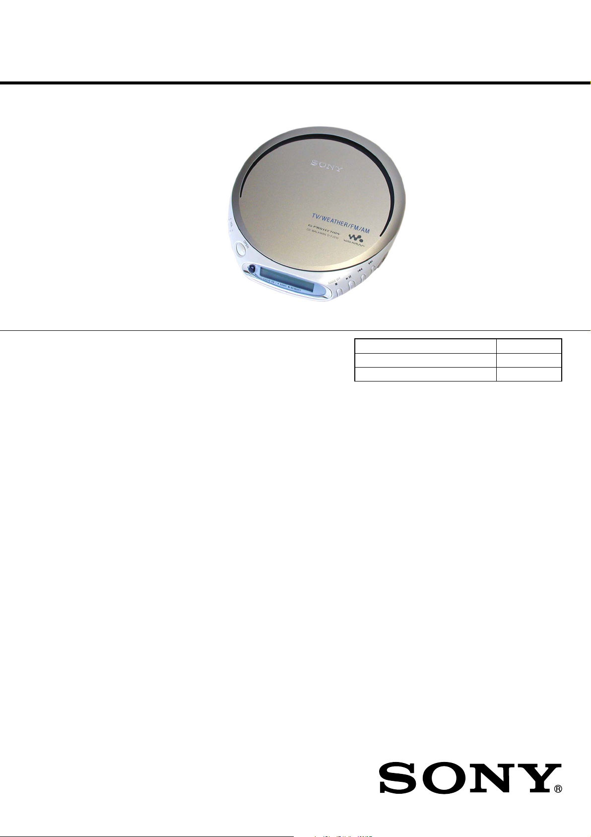
D-FJ210/FJ215
SERVICE MANUAL
Ver 1.0 2003.02
Photo : D-FJ210
SPECIFICATIONS
System
Compact disc digital audio system
Laser diode properties
Material: GaAlAs
Wavelength: λ = 780 nm
Emission duration: Continuous
Laser output: Less than 44.6 µW (This output is the value measured at a
distance of 200 mm from the objective lens surface on the optical pick-up
block with 7 mm aperture.)
D-FJ210 :
Frequency range (10k/9k switch)
10 kHz step:
TV: 2 - 13 ch
WB (weather band): 1 - 7 ch
FM: 87.5 - 108.0 MHz
AM: 530 - 1710 kHz
9 kHz step:
TV: 2 - 13 ch
WB (weather band): 1 - 7 ch
FM: 87.5 - 108.0 MHz
AM: 531 - 1710 kHz
D-FJ215 :
Frequency range (Chinese model)
FM: 87.5 - 108.0 MHz
AM: 531 - 1602 kHz
Frequency range (10k/9k switch) (except Chinese model)
•9 kHz step:
FM: 87.5 - 108.0 MHz
AM: 531 - 1 602 kHz
• 10 kHz step:
FM: 87.5 - 108.0 MHz
AM: 530 - 1 710 kHz
TV/WB/FM/AM PORTABLE CD PLAYER D-FJ210
FM/AM PORTABLE CD PLAYER D-FJ215
US Model
D-FJ210
E Model
Australian Model
Chinese Model
D-FJ215
Model Name Using Similar Mechanism D-EJ360
CD Mechanism Type CDM-3325ER
Optical Pick-up Type DAX-25E
Power requirements
For the area code of the model you purchased, check the upper left side of
the bar code on the package.
•Two Sony NH-7WMAA rechargeable batteries: 1.2 V DC x 2
• Sony NH-WM2AA rechargeable batteries: 1.2 V DC x 2
•Two LR6 (size AA) batteries: 1.5 V x 2 DC
• AC power adaptor (DC IN 4.5 V jack):
US model: 120 V, 60 Hz
E13 model: 220 - 230 V, 50/60 Hz
Australian model: 240 V, 50 Hz
Hong Kong model: 230 V, 50 Hz
Chinese model: 220 V, 50 Hz
Dimensions (w/h/d) (without projecting parts and controls)
Approx. 136 x 26 x 150 mm (5 3⁄8 x 1 1⁄16 x 6 in.)
Mass (excluding accessories)
Approx. 205 g (7.3 oz)
Operating temperature
5°C - 35°C (41°F - 95°F)
Design and specifications are subject to change without notice.
Supplied Accessories
FJ-210 :
Headphones/earphones with the remote control (1)
9-877-064-01
2003B0200-1
© 2003.02
Sony Corporation
Personal Audio Company
Pubulished by Sony Engineering Corporation

D-FJ210/FJ215
FJ-215 :
AC power adaptor (1)
Headphones/earphones with remote control (1)
Rechargeable batteries (2)
Battery carrying case (1)
DANGER
Invisible laser radiation when open and interlock failed or defeated.
Avoid direct exposure to beam.
CAUTION
Use of controls or adjustments or performance of procedures other
than those specified herein may result in hazardous radiation
exposure.
Flexible Circuit Board Repairing
• Keep the temperature of the soldering iron around 270°C during
repairing.
• Do not touch the soldering iron on the same conductor of the
circuit board (within 3 times).
• Be careful not to apply force on the conductor when soldering or
unsoldering.
Notes on chip component replacement
• Never reuse a disconnected chip component.
• Notice that the minus side of a tantalum capacitor may be damaged by heat.
TABLE OF CONTENTS
Specifications ............................................................................ 1
1. SERVICING NOTES ................................................... 3
2. GENERAL
Locating the Controls ......................................................... 3
3. DISASSEMBLY
3-1. Upper Lid ASSY, Cabinet (Upper) Sub ASSY ........... 4
3-2. MD ASSY, Main Board .............................................. 5
3-3. “Motor ASSY (Sled) (M902)”,
Optical Pick-up (DAX-25E),
“Motor ASSY, Turn Table (Spindle) (M901)” ............ 5
4. ELECTRICAL ADJUSTMENS ............................... 6
5. DIAGRAMS
5-1. Block Diagram –CD SECTION– .............................. 9
5-2. Block Diagram –Tuner SECTION– ........................ 10
5-3. Printed Wiring Boards (FJ215 only) –Side A– ......... 11
Printed Wiring Boards (FJ215 only) –Side B– ........ 12
5-4. Printed Wiring Boards (FJ210 only) –Side A– ........ 13
Printed Wiring Boards (FJ210 only) –Side B– ........ 14
5-5. Schematic Diagram –MAIN SECTION (1/4)– ....... 15
5-6. Schematic Diagram –MAIN SECTION (2/4)– ....... 16
5-7. Schematic Diagram –MAIN SECTION (3/4)– ....... 17
5-8. Schematic Diagram –MAIN SECTION (4/4)– ....... 18
5-9. IC Pin Function Description ..................................... 22
6. EXPLODED VIEWS
6-1. Cabinet Section ......................................................... 24
6-2. Optical pick-up Section (CDM-3325ER) ................. 25
7. ELECTRICAL PARTS LIST ................................... 26
z
UNLEADED SOLDER
Boards requiring use of unleaded solder are printed with the
lead-free mark (LF) indicating the solder contains no lead.
(Caution: Some printed circuit boards may not come printed
with the lead free mark due to their particular size.)
: LEAD FREE MARK
Unleaded solder has the following characteristics.
• Unleaded solder melts at a temperature about 40°C higher
than ordinary solder.
Ordinary soldering irons can be used but the iron tip has to
be applied to the solder joint for a slightly longer time.
Soldering irons using a temperature regulator should be set
to about 350°C.
Caution: The printed pattern (copper foil) may peel away if
the heated tip is applied for too long, so be careful!
• Strong viscosity
Unleaded solder is more viscous (sticky, less prone to
flow) than ordinary solder so use caution not to let solder
bridges occur such as on IC pins, etc.
• Usable with ordinary solder
It is best to use only unleaded solder but unleaded solder
may also be added to ordinary solder.
SAFETY-RELATED COMPONENT WARNING!!
COMPONENTS IDENTIFIED BY MARK 0 OR DOTTED LINE
WITH MARK 0 ON THE SCHEMATIC DIAGRAMS AND IN THE
PA RTS LIST ARE CRITICAL TO SAFE OPERATION.
REPLACE THESE COMPONENTS WITH SONY PARTS WHOSE
PA RT NUMBERS APPEAR AS SHOWN IN THIS MANUAL OR IN
SUPPLEMENTS PUBLISHED BY SONY.
2
SECTION 1
SERVICING NOTES
NOTES ON HANDLING THE OPTICAL PICK-UP BLOCK OR
BASE UNIT
The laser diode in the optical pick-up block may suffer electrostatic
breakdown because of the potential difference generated by the charged
electrostatic load, etc. on clothing and the human body. During repair,
pay attention to electrostatic breakdown and also use the procedure in
the printed matter which is included in the repair parts.
The flexible board is easily damaged and should be handled with care.
NOTES ON LASER DIODE EMISSION CHECK
The laser beam on this model is concentrated so as to be focused on the
disc reflective surface by the objective lens in the optical pick-up block.
Therefore, when checking the laser diode emission, observe from more
than 30cm away from the objective lens.
Before Replacing the Optical pick-up Block
Please be sure to check thoroughly the parameters as per the “Optical
pick-up Block Checking Procedure” (Part No. : 9-960-027-11) issued
separately before replacing the optical Pick-up block.
Note and specifications required to check are given below.
• FOK output : IC601 yg pin
When checking FOK, remove the lead wire to disc motor.
• RF signal P-to-P value : 0.45 to 0.75Vp-p
D-FJ210/FJ215
Laser Diode Checking Methods
During normal operation of the equipment, emission of the laser diode
is prohibited unless the upper panel is closed while turning ON the S809
(push switch type).
The following two checking methods for the laser diode are operable.
Method :
Emission of the laser diode is visually checked.
1. Open the upper lid.
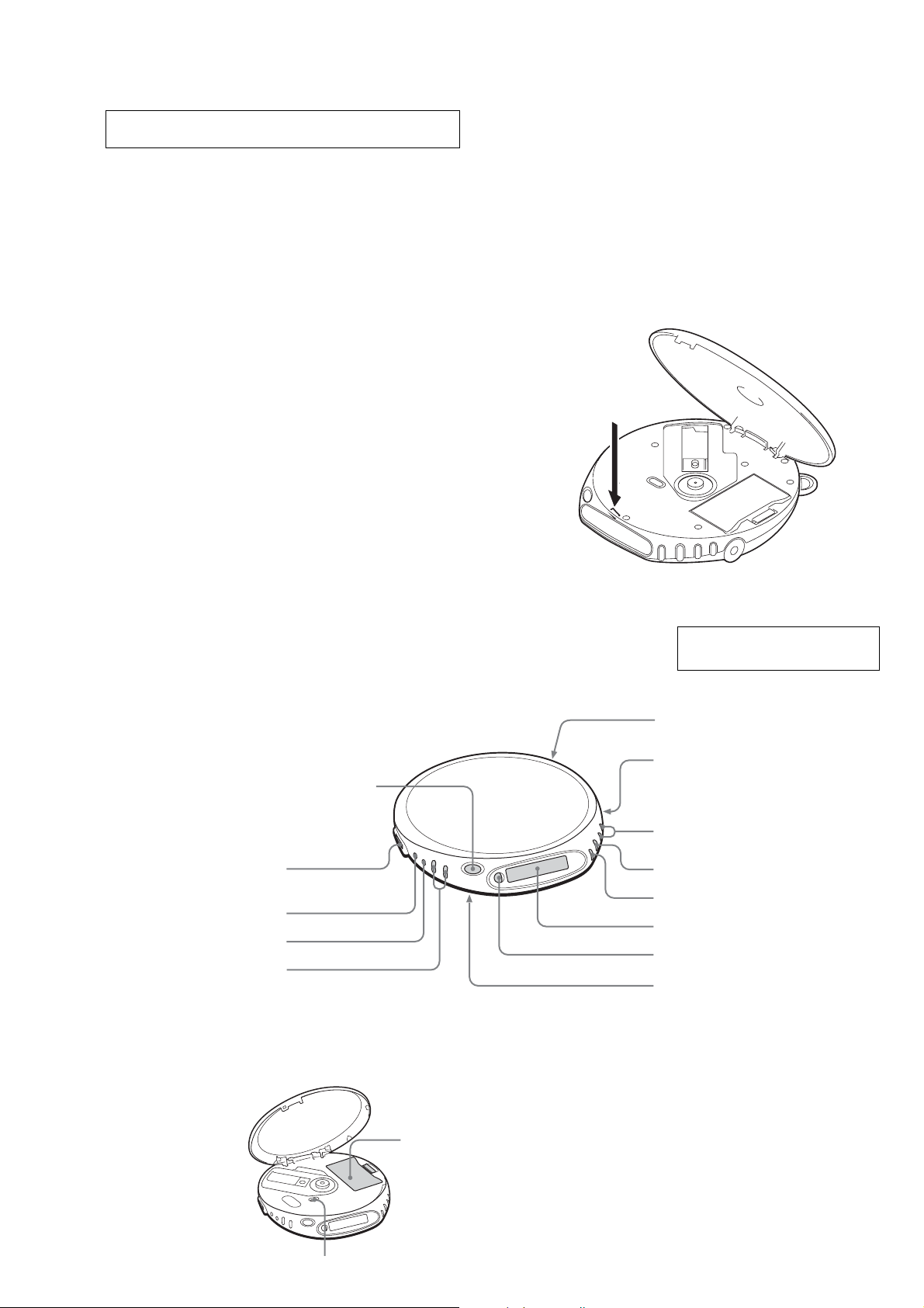
2. Push the S809 as shown in Fig. 1 .
3. Check the object lens for confirming normal emission of the laser
diode. If not emitting, there is a trouble in the automatic power
control circuit or the optical pick-up. During normal operation, the
laser diode is turned ON about 2.5 seconds for focus searching.
S809
LOCATING THE CONTROLS
CD player (front)
i (headphones) jack
SOUN/AVLS
P MODE/ F
VOL +*/–
*The button has a tactile dot.
OPEN
SECTION 2
GENERAL
Fig.1 Method to push S809
This section is extracted from
instruction manual.
Strap holes
DC IN 4.5 V
(external power
input) jack
.>
u*
x
• RADIO OFF (D-FJ210)
x
/ CHG • RADIO OFF (D-FJ215)
Display
RADIO ON/BAND • MEMORY
HOLD
CD player (inside)
G-PROTECTIO
Battery Compartment
3
D-FJ210/FJ215
z
The equipment can be removed using the following procedure.
SECTION 3
DISASSEMBLY
MD ASSY “Motor ASSY (Sled) (M902)”, Optical pick-up (DAX-25E),
Set
Upper lid ASSY,
Cabinet (upper) sub ASSY
Main board
Note : Follow the disassembly procedure in the numerical order given.
3-1. UPPER LID ASSY, CABINET (UPPER) SUB ASSY
5
Upper lid Assy
7
Ten screws (B2)
4
2
“Motor ASSY, turn table (spindle) (M901)”
• CAUTION DURING ASSEMBLY
1
Spring (L)
2
1
Open
6
3
Spring (R)
0
Cabinet
(upper) sub ASSY
9
8
Four craws
5
6
Spring (L)
4
1
3
Spring (R)
2
4
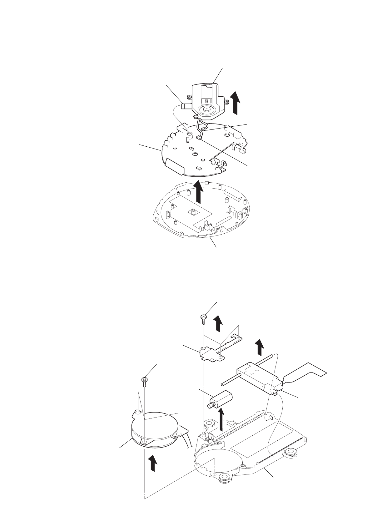
3-2. MD ASSY, MAIN BOARD
)
7
MAIN board
1
CN601
5
MD ASSY
4
2
Connector (CN401)
3
Connector (CN402
D-FJ210/FJ215
6
Cabinet (lower) sub ASSY
3-3. “MOTOR ASSY (SLED) (M902)”, OPTICAL PICK-UP (DAX-25E), “MOTOR ASSY, TURN TABLE (SPINDLE) (M901)”
1 Three screws
(B1.7x4)
2
3 Cover, Gear
8 Three screws
(B1.7x4)
6
0 Motor ASSY, Turn table
(Spindle) (M901)
5 Motor ASSY
(Sled) (M902)
9
7 Optical pick-up
(DAX-25E)
4
Chassis
5
D-FJ210/FJ215
R73
TUNER SECTION
AM section
BAND : AM
AM RF signal
generator
30% amplitude modulation by 400Hz
signal.
Output level : as low as possible
FM section
BAND :FM
TJ3
(FM RF IN)
[MAIN BOARD]
(Side A)
TJ304
102
J606
06
TJ307
VDR305
TJ605
TJ801
VDR302
TJ802
TJ410
set
C325
TJ608
AA
D306
D
TJ3
(FM RF IN)
L606
TJ611
R601
TAP1
TJ5
ELECTRICAL ADJUSTMENTS
0 dB = 1µV
Put the lead-wire
antenna close to
the set.
FM RF signal
generator
0.01
µ
F
33.75kHz frequency deviation
by 1kHz signal.
Output level :
as low as possible
FJ215:CH
C810
L4
D3
FL2:FJ215
FL1:FJ210
TJ10
C44
16
FJ120
R2
C22
C9
1
Ω
FJ210
TJ6
IC1
level meter
R873
30
SECTION 4
• Repeat the procedures in each adjustment several times, and the
frequency coverage and tracking adjustments should be finally
done by the trimmer capacitors.
< > : 9kHz step
AM FREQUENCY COVERAGE ADJUSTMENT
Adjust parts Frequency display
L5 530kHz <531kHz>
Confirmation 1,710kHz <1,602kHz>
AM TRACKING ADJUSTMENT
Adjust for a maximum reading on level meter.
L1 620kHz <621kHz>
CT1 1,400kHz <1,395kHz>
FM FREQUENCY COVERAGE ADJUSTMENT
Frequency display Reading on digtal voltmeter
Confirmation 87.5MHz Standard value : 4.3–5.7V
L2 108MHz
C21
D2
L3
R4
C8
TJ8
L2
R844
R815
R75
TJ1
R66
C109
R74
R65
2
3
7
L4 87.5MHz
Confirmation 108MHz
TV/WB FREQUENCY COVERAGE ADJUSTMENT
FM TRACKING ADJUSTMENT
Adjust for a maximum reading on level meter.
Frequency display Reading on digtal voltmeter
Confirmation TV : 2ch Standard value : 0.46–0.54V
TV/WB TRACKING ADJUSTMENT
Adjust for a maximum reading on level meter.
L3 162.55MHz [WB : 1ch]
CT2 215.75MHz [TV : 13ch]
Reading on digtal
voltmeter
Adjustment value : 0.7V
Standard value : 0.2–1.4V
Adjustment value : 5.0V
<4.4V>
Standard value : 4.3–5.7V
<3.7–5.2V>
Adjustment value : 9.5V
Standard value : 9.0–10.0V
FJ210 only
FJ210 only
phones jack (J301)
6
Adjustment Location : Main board
R73
r
Frequency Coverage Adjustment
Setting :
D-FJ210/FJ215
[MAIN BOARD]
(Side A)
TJ304
102
J606
06
TJ307
VDR305
TJ605
TJ801
VDR302
TJ802
TJ410
AA
D306
C325
D
TAP1
TJ3
(FM RF IN)
FL2:FJ215
FL1:FJ210
TJ5
L606
TJ608
TJ611
R601
TJ10
Adjustment Location :
[MAIN BOARD] (SIDE B)
FJ215:CH
C810
D3
R2
C9
TJ6
(TU GND)
1
C44
L4
FJ120
C22
IC1
TJ6 (TU GND)
R873
FJ210
C21
D2
L3
R4
C8
TJ1
(VT)
30
TJ8
2
L2
digital voltmete
TJ1 (VT)
R844
R815
R65
3
7
(DC range)
R75
R66
C109
R74
*
L3 : TV/WB Traking Adjustment
*
CT2 : TV/WB Traking Adjustment
L4 : FM Traking Adjustment
L2 : FM Frequency Coverage Adjustment
L5 : AM Frequency Coverage Adjustment
L1 : AM Tracking Adjustment
CT1 : AM Tracking Adjustment
: FJ210 only
*
7
D-FJ210/FJ215
p
B
3
CD SECTION
The CD section adjustments are done automatically in this set.
Precautions for Check
1. Perform check in the order given.
2. Use YEDS-18 disc (Part No.: 3-702-101-01) unless otherwise
indicated.
3. Power supply voltage requirement : DC4.5 V in DC IN jack.
(J401)
VOLUME button : Minimum
HOLD switch : OFF
RF Level Check
Condition:
• Hold the set in horizontal state.
Connection:
oscilloscope
(AC range)
TJ601(RF)
[MAIN BOARD]
(Side A)
TJ303
FJ215:CH
C624
C619
R616
L602
601
C633
R615
IC601
C632
R614
C618
F
FB301
TJ305
FB101
R306
26
H
FJ215:C
25
R613
C609
C608 C607
R612
C614
C613
C605
TJ601
(RF)
C604
C612
5
TJ401(A GND)
C325
VDR305
VDR302
TJ307
TJ605
TJ801
TJ802
TJ410
(A GND)
TJ608
TJ606
C606
AA
D306
R601
D
TJ611
H
FJ215:C
FL2:FJ215
FL1:FJ210
TJ10
C810
D
R2
C9
1
C44
TAP1
TJ3
TJ5
L606
Procedure:
1. Connect the oscilloscope to the test point TJ601(RF) on the
MAIN board.
2. Set a disc. (YEDS-18)
3. Press the u button.
4. Check the oscilloscope waveform is as shown below.
A good eye pattern means that the diamond shape (◊) in the center of the waveform can be clearly distinguished.
RF Signal reference Waveform (Eye Pattern)
VOLT/DIV : 100 mV (With the 10 : 1 probe in use)
TIME/DIV : 500ns
RF level
0.45 to 0.75 Vp-
To watch the eye pattern, set the oscilloscope to AC range and
increase the vertical sensitivity of the oscilloscope for easy
watch-ing.
5. Stop revolving of the disc motor by pressing the x button.
8
5-1. BLOCK DIAGRAM –CD SECTION–
IC602
D-RAM(16M)
SECTION 5
DIAGRAMS
IC603
D-FJ210/FJ215
FJ215FJ210
D-RAM(4M)
OPTICAL
PICK-UP
BLOCK
(DAX-25E)
OP IC
FOCUS
COIL
TRACKING
COIL
M902
SLED
MOTOR
M901
SPINDLE
MOTOR
VCC
RF
OP_G-SW
OP_STB
A
A
E
F
LD
PD
M
M
D0-3 A0-10
2,3,24,25 9-12,15-19,21,8
VCC1_2.2V
LD
DRIVER
Q601
VCC1_2.2V
F+
F-
T+
T-
S+
S-
W
V
U
+VBAT
L403
5 23 4
16 17
DETI
RFGO
RFI
13
A
9
B
8
E
6
F
7
RFDC
88
LD-SW
2
FO3
44
RO3
42
FO2
48
RO2
46
FO1
52
RO1
50
W_O
6
V_O
4
U_O
2
COMCOM
80
VM1
53
VM12
49
45
VM23
41
VM3
SPVCC
1
RF
AMP
A/D
APC
PD
3
CH3
H
BRIDGE
CH2
H
BRIDGE
CH1
H
BRIDGE
CH4
H
BRIDGE
IC403 (1/2)
FOCUS/TRACKING COIL DRIVE
SLED/SPINDLE MOTOR DRIVE
EFM
DEMODULATOR
LEVEL
SHIFTER
LEVEL
SHIFTER
POWER_LT_I
I/F
D0-3 A0-9
2,3,24,25 9-12,14-18,5
87,88,84,85 97-100,96-91,82
D0-D3
SERVO
PWM
FDOP
FDON
TDOP
TDON
75 74 77 76 79 78 72 73 71 504947533738
FIN-
TIN-
FIN+
TIN+
FIN3
60
RIN3
59
FIN1
56
RIN1
55
FIN2
58
RIN2
57
BBK
70
PWM
72
34
SYNC
74
FG
40
XSDTO
39
XCSK
38
WAKEUP
37
35
H_RESET
36
XRST_I
SDOP
SIN+
FIN+
FINSIN+
SIN-
TIN+
TIN-
CPOL
SLVOP
SYNC
SUB CODE
PROCESSOR
SDON
CLVON
CLVOP
SIN-
CPOL
CLVOP
DEFFERENTIAL
Q407
A0-A10
CLKDRV
SYNC
XRAS
XCAS
4 23 3
90 83 89
XCAS
XRAS
CLOCK
OSC
X_O
X601
16.934MHz
XWE
XWE
X_I
WARK-UP
DETECT
Q801,802
IC601
RF AMP,SERVO
DIGITAL SIGNAL PROCESSOR
D-RAM CONTROLLER
D/A CONVERTER
SIO
CLK4M
SCLK_I
SDTO_I
SDTI_O
D802
SRW_I
48
15
SRW_O
X_I
2
OP_G-SW_O
79
XOPSTBY_O
78
WP/KEY2_RM_I
33
FG_I
72
XPOWLT_O
14
SDTI_I
16
SDTO_O
17
SCK_O
18
XWAKEUP_O
66
8
XREST_I
XRST_O
76
VCPU_2.0V
P-OFF_I
SCOR
XBUSY_O
SCOR_I
XBUSY_I
POWER-OFF_O
TO
TUNER
SECTION
(Page 10)
DAC
DEFDCT_O
GFS_O
FOK_O
657064524345
6711371177
GFS_I
FOK_I
DEFECT_I
WP/AD_KEY1
AD_KEY_2
2523 28 40
KEY MATRIX
S801 S805
| |
S804 S808
C
LDACO
RDACO
DVDDIO
AVDD2 2.25V
DVDDV 1.5V
VCHK
TIST
CLK4M_2
RESET2
TEST
TEST
IC801(2/2)
SYSTEM
CONTROL
MICON
TU_L
TU_R
31
29
36
80
86
34
40
51
5
PGM_SDTO
PGM_SDTI
68674
PGM_SDTI_I
PGM_SDTO_O
VCC2_2.0V
VCC1_2.2V
VCPU_1.5V
PGM_SCK
PGM_SC_SEL
7369
PGM_SCK_O
PGM_SC_SEL
WP/XOPEN_I
S809
(OPEN)
33
35
CD_L-I
32
CD_I_R
36
31
12
HOLD
OFF ON
STB_HPSW_I
26
HPSW_O
WP/AD_RMKEY
HOLD_I
S810
.
IC301
PRE EQ AMP/EVR/
HADPHONE AMP
AD_CHGMNT
TUNER_ON_I
AD_BATTMNT
AD_DCINMNT
GPROSW
AVCPU
38
19
S811
G.PROTECTION
OFF ON
4
VCC2
17
VCC1
44
IN SEL
POWER-L_O
CENTER-AMP
POWER-R_O
BASS-H/L-SW TU_BASS2
MUTE-SW_I
22
34
+V BAT
24
27
ADVREF
20
VCPU_2.0V
BASS-SW
VOL-CTL_I
BEEP_I
VCC2_2.0V
7
6
5
25
26
14
3
1
VCC1_2.2V
VCPU_2.0V
Q401
CHARGE
SWITCH
XTU_BASS1
PWM
BEEP
AMUTE
+VBAT
VCC2_2.0V
A
IC403 (2/2)
POWER CONTROL
VMMNT
66
VCC2
18
17
VCC1
19
VCPU 2.0V
CHGMNT
67
DCIN
61
REGB
62
DET
63
CHGB
65
+VBAT
SWITCH
Q402, 403
BATT_MNT
TU_ON
RM_KEY
PGM_SC_SEL
OPEN_DTS
HOLD
AD_KYE2
AD_KYE1
SDTO
SCK
TO
TUNER
SECTION
(Page 10)
D405
D402
SEM
SEO
GSW
VCC
VCC0
STNG
VIN
BATM1
BATM2
DCIN_S
TO
D
TUNER
SECTION
(Page 10)
J301
ANT
i
VCPU_2.0V
VCPU_1.5V
23
22
21
20
16
25
L404
LG
8
12
68
69
64
L401
L402
TO
TUNER
B
SECTION
(Page 10)
Q406
L410
Q405
D408
Q408
Q404
DRY BATTERY
SIZE "AA"
(IEC DESIGNATION LR6)
2PCS, 3V
J401
DC IN 4.5V
!
• SIGNAL PATH
: FM
: CD PLAY
99
D-FJ210/FJ215
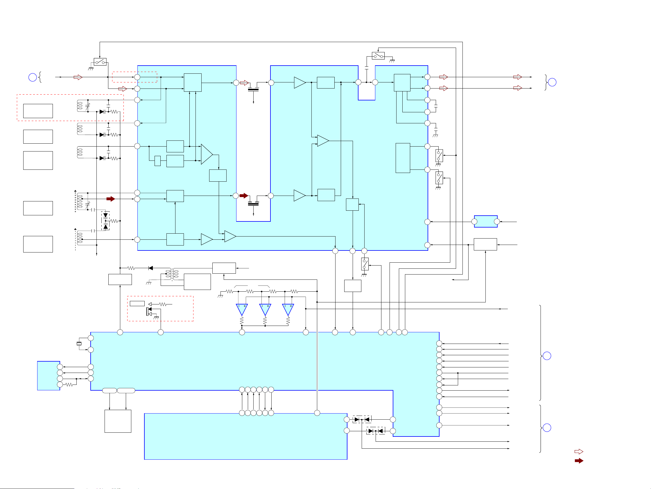
5-2. BLOCK DIAGRAM –TUNER SECTION–
TO
CD
SECTION
(Page 9)
D
FJ210
L3, CT2
TV
TRACKING
L4
FM
TRACKING
L2
FM/TV
FREQUENCY
COVERAGE
L1, CT1
AM
TRACKING
L5
AM
FREQUENCY
COVERAGE
ANT
(FM/TV OSC)
IC4
EEPROM
CS
SK
D1
D0
CT2
L3
(TV RF)
L4
(FM RF)
L2
L1
AM
FERRITE-ROD
ANTENNA
CT1
L5
(AM OSC)
CF5
(75KHz)
1 32
2
3
4
D2
D3
D4
TU-VCC
74
X_O
X_I
75
EEP-CS_O
31
EEP-SK_O
30
EEP DO/DI_IO
12 13
SW
IF-COUNT_O
REQ-SW
2019
Q15
IF_I
Q7
Q8
Q4
TV/FM/AM FRONTEND, FM MPX
FJ210
(VT)
LPF
Q12,13
65 21 35 42 71 64 61 52 59 55
EO(D01)_O
TV-RF
1
FM-RF
2
TV-RF_O
30
FM-RF_O
29
FM/TV-OSC
24
AM_BP
28
AM-RF_I
27
AM-OSC
25
D6
EXCEPT FJ215:CH
S1
STEP
10K
R
9K
1/2
AM-STEP_I
IC1
TV
OSC
FM
OSC
AM
MIX
AM
OSC
T1
VCPU_2.0V
FM/TV
MIX
BUFF
AM-MIX_O
BUFF BUFF
DC-DC
CONVERTOR
Q14
COMPARATOR
FM-MIX_O
1/8
or
1/16
B+ SWITCH
Q10,11
IC5,6
LEVEL
CF2
4
TU-VCC
CF3
5
TU-VCC
+VBAT
FM-IF_I DET_O
8
AM-IF_I
10
IC5IC6
32
5631
174
NC
FM-IF
AM-IF
RM-KEY_I
FM
DET
IF BUFF
AM
DEF
OSC_O
23
TV/FM/AM_I
BUFFER
IC3
TUNER CONTROL
LCD-REQ_I
XL/O-I
CD-ON_I
RESET-TU_I
SDU-SDO_O
COM1-4 S1-17
1-4 5-20,25
28 33 39 73 47 54
ACK-CD_O
MPX_I
IF-REQ_O
FM
MPX
PW SW
FM/TV/AM
AD-DC_REF
BAND-CTL2_O
BAND-CTL1_O
MONO/LOCAL-CTL_O
PLAY-KEY-CLT_O
L_O
16
R_O
15
LPF2A
17
LPF2B
18
LPF1
14
MODE1 Q2
21
MODE2
22
45
RF-VCC
26
TU-VCC
BATT_I
51
29
48
46
43
26
36
34
38
37
TU-HOLD_I
XLID-OPEN_I
CDU-SCK_I
CDU-SDI_I
AD-KEY2_I
AD-KEY1_I
TU-ON_O
SC-SEL_I
C
TO
CD
SECTION
(Page 9)
TU_L
TU_R
Q3
IC2
+1.6V REG.
VOUT VIN
1 3
B+ SWITCH
Q5,9
+VBAT
VCPU_2.0V
RM_KEY
HOLD
OPEN_DTS
SCK
SDTO
BATT_MNT
AD-KEY1
AD-KEY2
TU_ON
PGM_SC_SEL
B
TO
CD
SECTION
(Page 9)
LCD1
LIQUID
CRYSTAL
DISPLAY
IC801(1/2)
SYSTEM
CONTROL
MICON
39 37 70 75 10 9
XL_O
CD_ON_O
LCD-REQ_O
SDTI_I_TU
RESET-TU_O
ACK_CD_I
10
29
AMUTE_O
BEEP_O
TUNER_POWER_O
10
D301
74 62
38
D302
TU_MUTE_O
TU_BEEP_O
49
TU-BASS_O
XTU-BASS_O
VOL_PWM_O
56
58
50
TU-BASS2
XTU-BASS1
PWM
BEEP
AMUTE
A
TO
CD
SECTION
(Page 9)
• SIGNAL PATH
: FM
: AM
• Abbreviation
CH : Chinese
 Loading...