Sony DF-20 Service manual
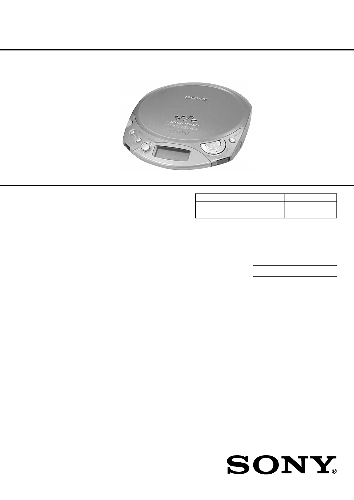
D-F20
SERVICE MANUAL
Ver 1.0 2001.05
SPECIFICATIONS
US Model
Model Name Using Similar Mechanism D-E220/E225/E226CK
CD Mechanism Type CDM-3123EBA
Optical Pick-up Name DAX-23E
CD player
System
Compact disc digital audio system
Laser diode properties
Material: GaAlAs
Wavelength: λ = 780 nm
Emission duration: Continuous
Laser output: Less than 44.6 µW (This output
is the value measured at a distance of 200 mm
from the objective lens surface on the optical
pick-up block with 7 mm aperture.)
D-A conversion
1-bit quartz time-axis control
Frequency response
20 - 20,000 Hz +1/–2 dB
(measured by EIAJ CP-307)
Output (at 4.5 V input level)
Headphones (stereo minijack)
Approx. 12 mW + Approx. 12 mW
at 16 ohms
Radio
Frequency range (STEP switch)
9 kHz step:
FM: 87.5 - 108.0 MHz
AM: 531 - 1,710 kHz
10 kHz step:
FM: 87.5 - 108.0 MHz
AM: 530 - 1,710 kHz
Antenna
FM: Headphones cord antenna
AM: Built-in ferrite bar antenna
General
Power requirements
For the area code of the model you purchased,
check the upper left side of the bar code on the
package.
• Two LR6 (size AA) batteries: 3 V DC
• AC power adaptor (DC IN 4.5 V jack):
120 V, 60Hz
Battery life* (approx. hours)
(When you use the CD player on a flat and stable
surface.)
Playing time varies depending on how the CD player
is used.
When using ESP RADIO
Two sony alkaline 24 25 66
batteries LR6(SG)
* Measured value by the standard of JEITA
(Japan Electronics and Information Technology
Industries Association).
** Charging time varies depending on how the
rechargeable battery is used.
Operating temperature
5°C - 35°C (41°F - 95°F)
Dimensions (w/h/d) (excluding projecting
parts and controls)
Approx. 161 × 26.3 × 130.3 mm
3/8 × 1 1/16 × 5 1/4 in.)
(6
Mass (excluding accessories)
Approx. 210 g (7.5 oz.)
Supplied accessories
For the area code of the location in which you
purchased the CD player, check the upper left
side of the bar code on the package.
Headphones (1)
Design and specifications are subject to change
without notice.
on off on
9-873-148-01
2001E0400-1
© 2001.5
FM/AM PORTABLE CD PLAYER
Sony Corporation
Personal Audio Company
Shinagawa Tec Service Manual Production Group
1

D-F20
Flexible Circuit Board Repairing
• Keep the temperature of the soldering iron around 270°C during
repairing.
• Do not touch the soldering iron on the same conductor of the
circuit board (within 3 times).
• Be careful not to apply force on the conductor when soldering
or unsoldering.
Notes on Chip Component Replacement
• Never reuse a disconnected chip component.
• Notice that the minus side of a tantalum capacitor may be
damaged by heat.
TABLE OF CONTENTS
1. SERVICE NOTE ................................................................. 3
2. GENERAL
Getting started ......................................................................... 4
3. DISASSEMBLY
3-1. “Lid, Battery Case”, Cabinet (Front) Assy.......................... 5
3-2. Lid Assy, Upper ................................................................... 5
3-3. Main Board, MD Assy ........................................................ 6
3-4. Optical Pick-up, Motor ....................................................... 6
4. ELECTRICAL ADJUSTMENTS
Tuner Section........................................................................... 7
CD Section .............................................................................. 8
5. DIAGRAMS
5-1. IC Pin Descriptions ............................................................. 9
5-2. Block Diagram –CD Section– ........................................... 13
5-3. Block Diagram –Tuner Section– ....................................... 14
5-4. Block Diagram –Power Supply Section– .......................... 15
5-5. Printed Wiring Board –Main Section– .............................. 16
5-6. Schematic Diagram –Main Section (1/3)– ......................... 18
5-7. Schematic Diagram –Main Section (2/3)– ......................... 19
5-8. Schematic Diagram –Main Section (3/3)– ......................... 20
5-9. IC Block Diagrams ............................................................ 21
6. EXPLODED VIEWS
6-1. Cabinet (Front) Section ..................................................... 24
6-2. Cabinet (Lower) Section ................................................... 25
6-3. CD Mechanism Deck Section (CDM-3123EBA) ............. 26
7. ELECTRICAL PARTS LIST ......................................... 27
SAFETY-RELATED COMPONENT WARNING!!
COMPONENTS IDENTIFIED BY MARK 0 OR DOTTED LINE
WITH MARK 0 ON THE SCHEMATIC DIAGRAMS AND IN
THE PARTS LIST ARE CRITICAL TO SAFE OPERATION.
REPLACE THESE COMPONENTS WITH SONY PARTS WHOSE
PART NUMBERS APPEAR AS SHOWN IN THIS MANUAL OR
IN SUPPLEMENTS PUBLISHED BY SONY.
2
SECTION 1
SERVICE NOTE
D-F20
NOTES ON HANDLING THE OPTICAL PICK-UP BLOCK
OR BASE UNIT
The laser diode in the optical pick-up block may suffer electrostatic breakdown because of the potential difference generated by
the charged electrostatic load, etc. on clothing and the human body.
During repair, pay attention to electrostatic breakdown and also
use the procedure in the printed matter which is included in the
repair parts.
The flexible board is easily damaged and should be handled with
care.
Precautions for Checking Emission of Laser Diode
Laser light of the equipment is focused by the object lens in the
optical pick-up so that the light focuses on the reflection surface
of the disc. Therefore, be sure to keep your eyes more then 30 cm
apart from the object lens when you check the emission of laser
diode.
Before Replacing the Optical Pick-Up Block
Please be sure to check throughly the parameters as par the “Optical Pick-Up Block Checking Procedures” (Part No.: 9-960-027-
11) issued separately before replacing the optical pick-up block.
Note and specifications required to check are given below.
• FOK output : IC601 eg pin
When checking FOK, remove the lead wire to disc motor.
• RF signal P-to-P value : 0.45 ± 0.1 Vp-p
• The repairing grating holder is impossible.
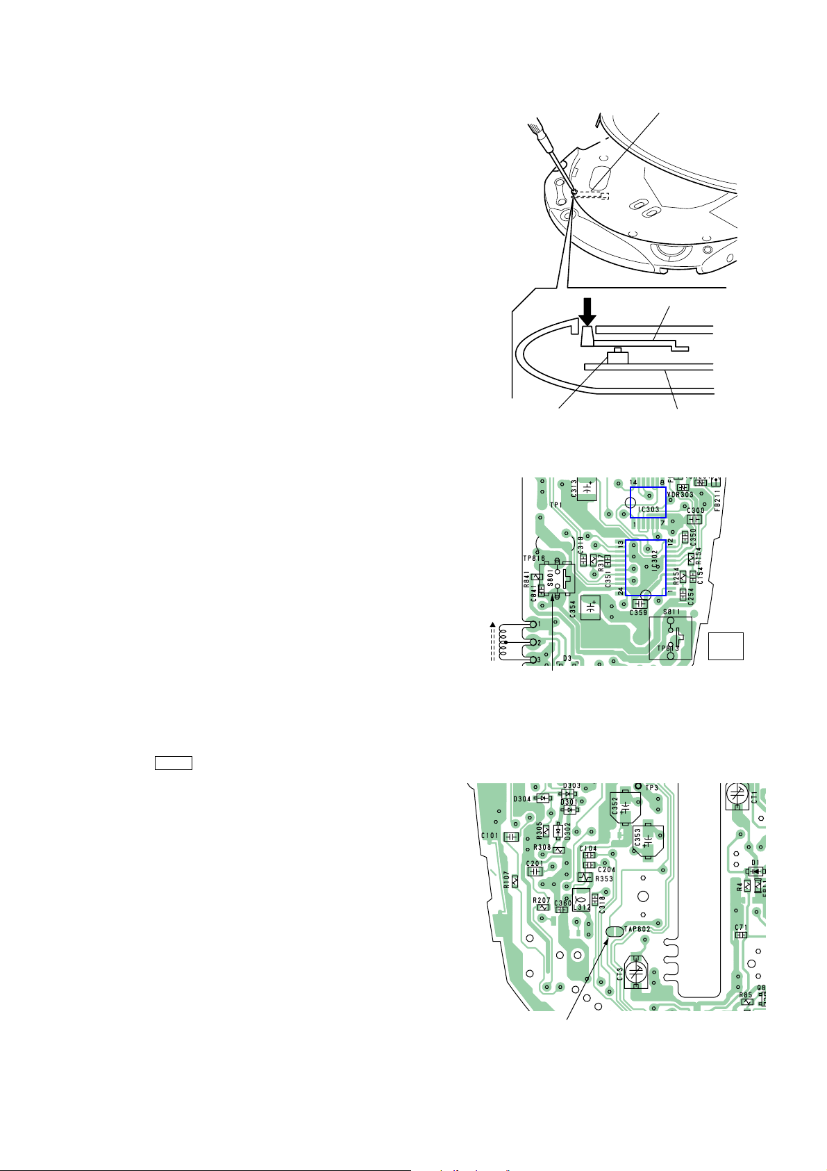
Laser Diode Checking Methods
During normal operation of the equipment, emission of the laser
diode is prohibited unless the upper lid is closed while turning ON
the S801. (push switch type)
The following two checking methods for the laser diode are
operable.
• Method:
Emission of the laser diode is visually checked.
1. Open the upper lid.
2. With a disc not set, turn on the S801 with a screwdriver having a
thin tip as shown in Fig.1.
or TAP802 is shorted as shown in Fig.2.
Note: Do not push the detection lever strongly, or it may be bent
or damaged.
3. Press the N X button.
4. Observing the objective lens, check that the laser diode emits
light.
When the laser diode does not emit light, automatic power
control circuit or optical pick-up is faulty.
In this operation, the objective lens will move up and down 5
times along with inward motion for the focus search.
S801
– MAIN BOARD (SIDE B) –
S801
CD DOOR
OPEN
L3
AM
FERRITE-
ROD
ANTENNA
S801
– MAIN BOARD (SIDE A) –
Fig. 1
RF-IN
detection lever
detection lever
main board
S811
SOUND/
PRESET
–
TAP802
Fig. 2
3
D-F20
SECTION 2
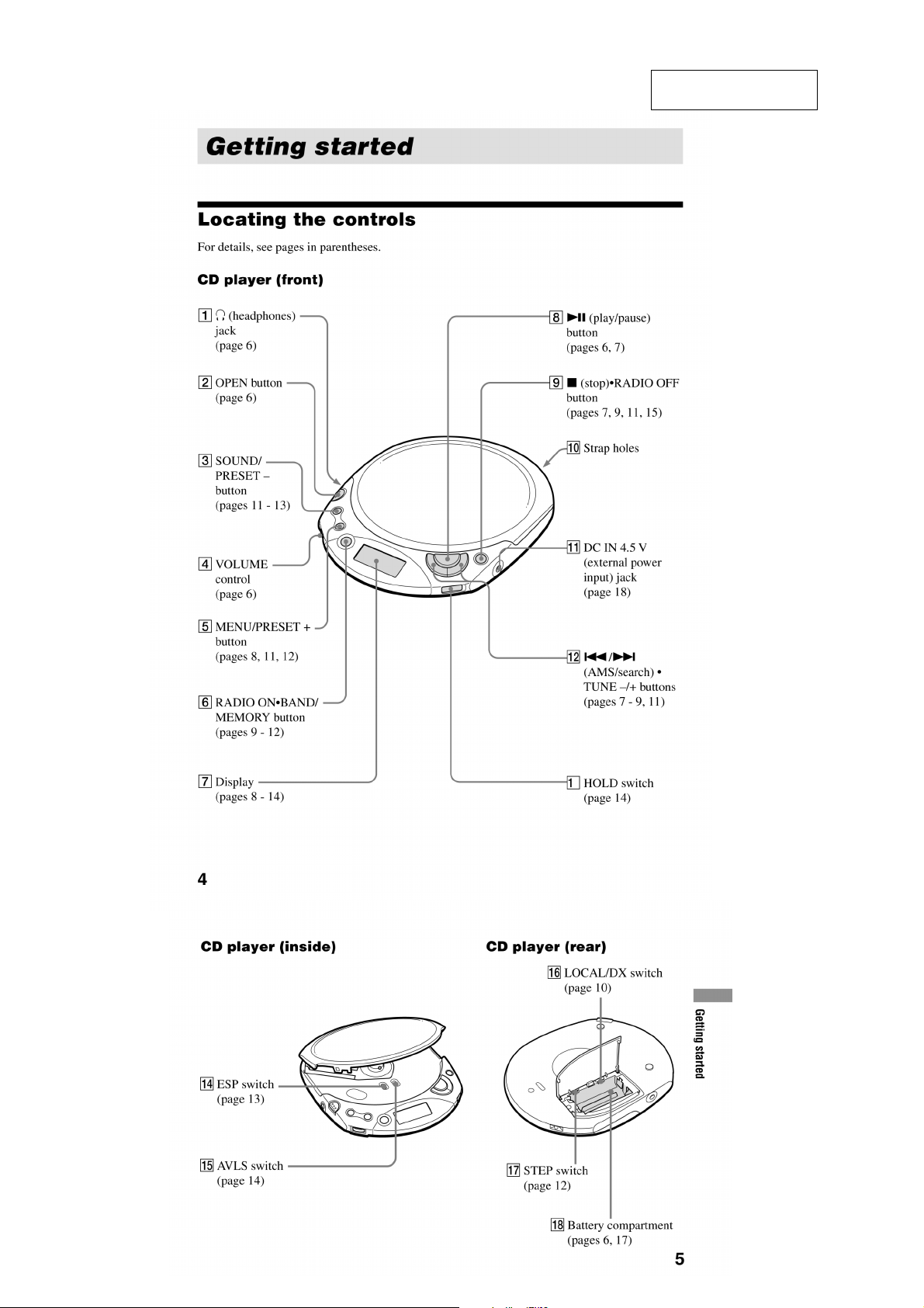
GENERAL
This section is extracted
from instruction manual.
4
SECTION 3
y
y
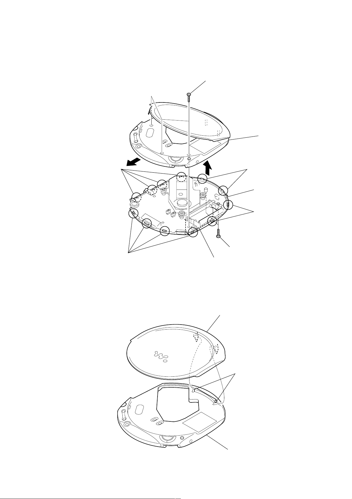
DISASSEMBLY
Note : Follow the disassembly procedure in the numerical order given.
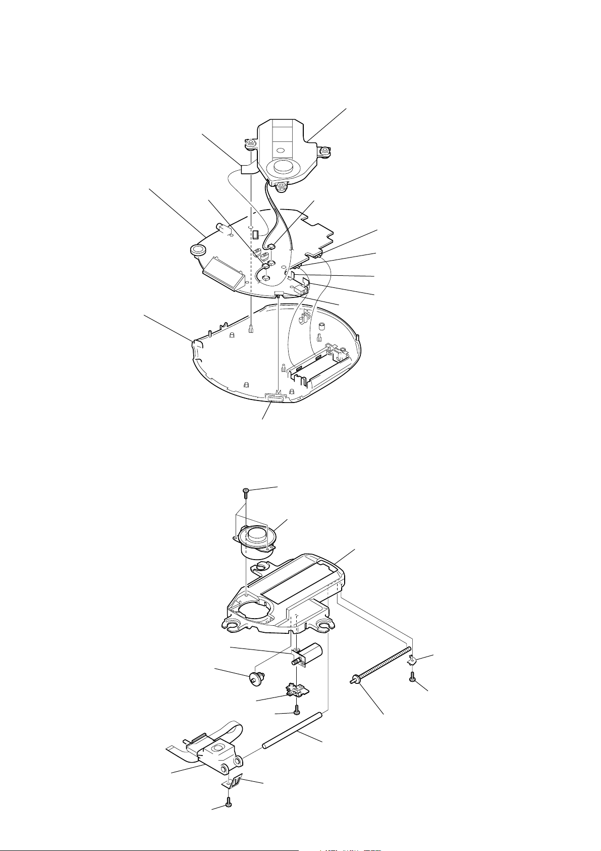
3-1. “LID, BATTERY CASE”, CABINET (FRONT) ASSY
8
1
B 2x10
0
cabinet (upper) ass
D-F20
3-2. LID ASSY, UPPER
6
claws
7
claws
9
3
B 2x10
2
lid, battery case
2
lid assy, upper
4
claws
boss
5
claws
1
claws
cabinet (front) ass
5
D-F20
)
t
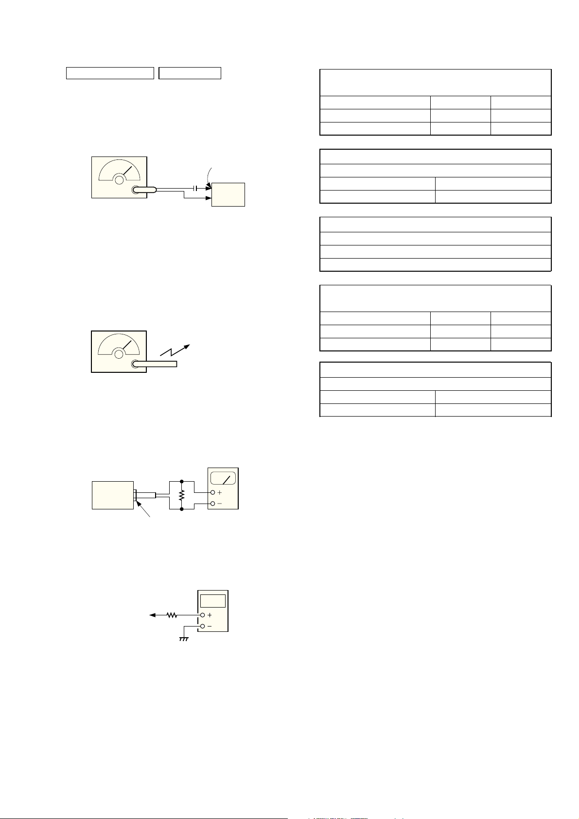
3-3. MAIN BOARD, MD ASSY
Note: When installing, fit the knob (HOLD) and S803.
1
CN501
7
MAIN board
cabinet (lower) sub assy
3
CN503
2
CN502
4
MD assy
S803
5
S812
6
S813
terminal (–), battery (BT402)
terminal (+.–), battery (BT400
3-4. OPTICAL PICK-UP, MOTOR
5
motor assy, sled (M501)
6
gear (B)
4
cover, gear
knob (HOLD)
3
B 1.7x5
1
B 1.7x5
2
motor assy, turntable (M502)
chassis
7
qa
screw (feed) assy
8
retainer, shaf
P 1.4x3.5
qd
shaft, standard
qs
pick-up block, optical
0
rack
9
B 1.4x2.3
6
)
SECTION 4
ELECTRICAL ADJUSTMENTS
D-F20
TUNER SECTION 0 dB = 1 µV
• FM Section
Setting:
RADIO ON•BAND/MEMORY button : FM
STEP switch : 10k
FM RF signal
generator
0.01
µ
F
75 kHz frequency
deviation by 1 kHz signal
output level : as low as possible
• AM Section
Setting:
RADIO ON•BAND/MEMORY button : AM
STEP switch : 10k
AM RF signal
generator
Put the lead-wire
antenna close to
the set.
TP3 (RF-IN)
set
FM FREQUENCY COVERAGE
CHECK
Frequency Display 87.5 MHz 108 MHz
Reading on Digital voltmeter 2.5 ± 1.5 V 7.0 ± 4.0 V
Adjustment Part <confirmation> <confirmation>
FM TRACKING ADJUSTMENT
Adjust for a maximum reading on level meter.
L2 CT1
87.5 MHz 108 MHz
AM IF ADJUSTMENT
Adjust for a maximum reading on level meter.
T1
450 kHz
AM FREQUENCY COVERAGE
CHECK
Frequency Display 530 kHz 1,710 kHz
Reading on Digital voltmeter 1.0 ± 0.5 V 5.2 ± 0.7 V
Adjustment Part <confirmation> <confirmation>
30% amplitude
modulation by
400 Hz signal
• Connecting Level Meter (FM and AM)
level meter
(range: 0.5–5 V ac
Ω
16
set
i
jack (J302)
• Connecting Digital Voltmeter (FM and AM)
digital
voltmeter
Ω
100 k
TP81 (VT)
AM TRACKING ADJUSTMENT
Adjust for a maximum reading on level meter.
L4 CT3
620 kHz 1,400 kHz
Adjustment Location: See page 8.
• Repeat the procedures in each adjustment several times, and the
frequency coverage and tracking adjustments should be finally
done by the trimmer capacitors.
• For FM adjustment, fix the FM RF coil (L1) as shown next page
and then perform tracking adjustment at L2 and CT1.
Lastly check the voltage value.
• For AM adjustment, fix the ferrite-rod antenna (L3) as shown
next page and then perform tracking adjustment at L4 and CT3.
Lastly check the voltage value.
7
D-F20
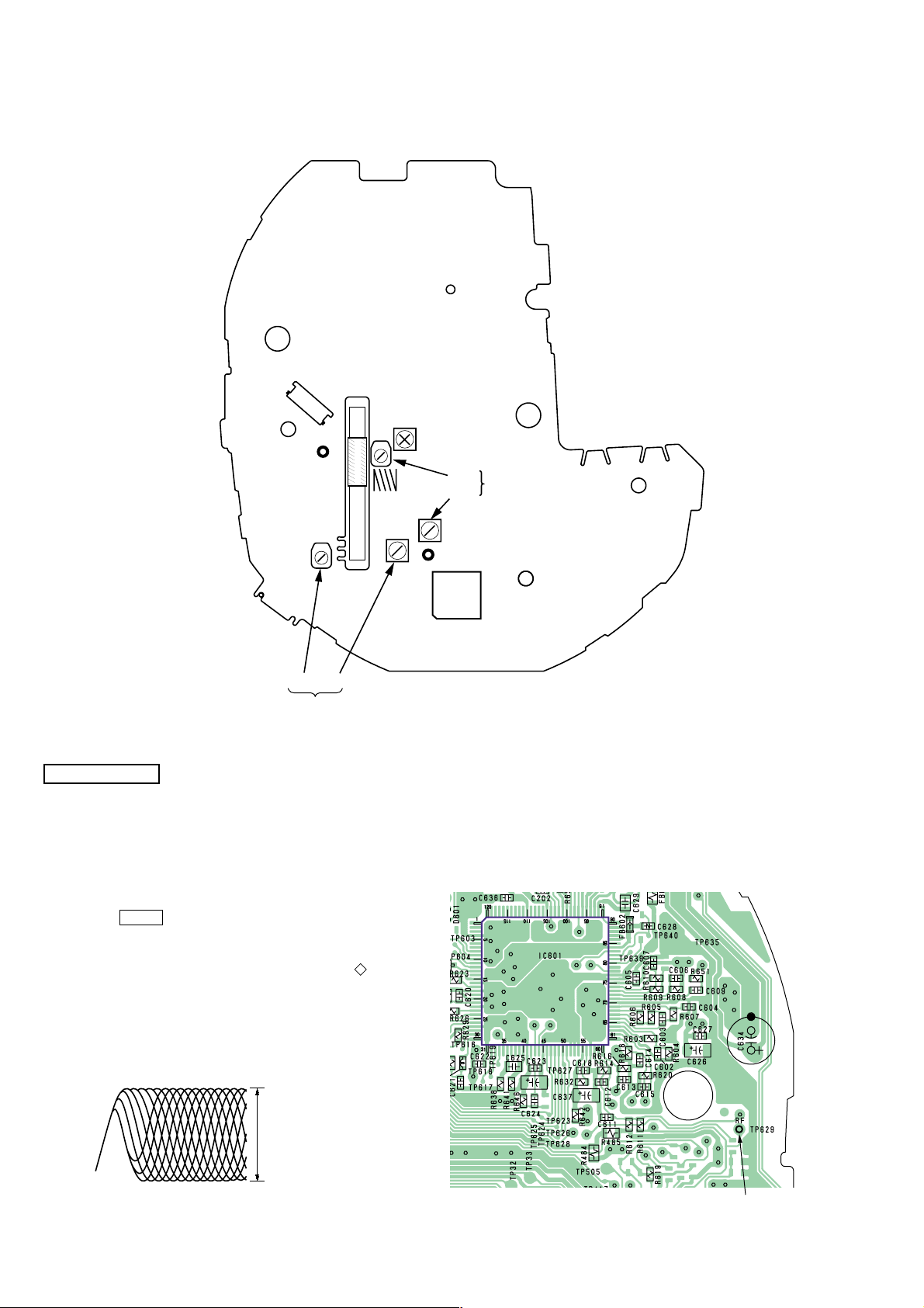
Adjustment Location:
– MAIN BOARD (SIDE A) –
CN501
AM IF ADJ
TP3
RF-IN
L3
L1
T1
CT1
FM TRACKING ADJ
L2
CT3 L4
AM TRACKING
ADJ
CD SECTION
CD section adjustments are done automatically in this set.
In case of operation check, confirm that focus bias.
FOCUS BIAS CHECK
1. Connect the oscilloscope between TP629 (RF) and GND on
main board.
2. Insert the disc (YEDS-18). (Part No. : 3-702-101-01)
3. Press the N X button.
4. Confirm that the oscilloscope waveform is as shown in the
figure below. (eye pattern)
A good eye pattern means that the diamond shape ( ) in the
center of the waveform can be clearly distinguished.
TP81
VT
IC61
Test Point:
– MAIN BOARD (SIDE B) –
• RF signal reference waveform (eye pattern)
VOLT/DIV : 20 mV (10 : 1 probe in use)
TIME/DIV : 500 nS
RF level :
±
0.1 Vp-p
0.45
When observing the eye pattern, set the oscilloscope for AC range
and raise vertical sensitivity.
8
TP629
RF

SECTION 5
DIAGRAMS
5-1. IC PIN DESCRIPTIONS
• IC61 TC9327AF-631 (TUNER PLL, LCD DRIVER)
Pin No. Pin Name I/O Pin Description
1 – 4 COM1 – 4 O LCD driver signal output
5 – 20 S1 – 16 O LCD driver signal output
21 AM STEP-I I AM 9K/10K tuning step select signal input (initialization)
22 DEST2-I I Bit2 tuner destination setting signal input (Fixed at “L” in this set)
23 DEST1-I I Bit1 tuner destination setting signal input (Fixed at “L” in this set)
24 DEST0-I I Bit0 tuner destination setting signal input (Fixed at “L” in this set)
25 XLOCAL/XMONO-DET-I I LOCAL/DX or MONO/STEREO ON-OFF switch detect signal input
26, 27 NC — Not used. (Open)
28 LCDREQ-I I LCD display request signal input
29 LID OPEN I CD door open detect signal input
30 EEP D0/D1-IO I/O Data signal input/output for EEPROM IC.
31 EEP SK-O O Clock signal output for EEPROM IC.
32 EEP CS-O O Chip select signal output for EEPROM IC.
33 XL/O-I I Line out signal input
34, 35 NC — Not used. (Open)
36 MEM-KEY (3-BIT) I Memory key signal input (Fixed at “H” in this set)
37 PRESET KEY I Not used in this set. (Open)
38 CD ACK-I O CD acknowledge signal output
39 CDON-IWP-CDU I CD ON request signal input (Wake-up tuner in sleep mode)
40 I/O (RESERVED) — Not used. (Open)
41 NC — Not used. (Open)
42 AD1 KEY I Set keys signal input
43 AD2 RMKEY I Remote key signal input (Fixed at “L” in this set)
44 AD3 BATT HIDC I Battery/HiDC level detect signal input
45 AD DC REF I Reference DC signal input of A/D.
46 SDI-I-CDU I Serial data signal input from system control IC.
47 SDO-O-CDU (RESERVED) O Serial data signal output to system control IC.
48 SCK-I-CDU I Serial clock signal input from system control IC.
49 TUBEEP-O O Beep sound control signal output
50 NC (I/O) — Not used. (Open)
51 XHOLD-I-SW I HOLD detect signal input
52 XAVLS-I-SW I AVLS detect signal input
53 XDC IN DET-I I DC-in detect signal input
54 TU ON-O O Tuner ON request signal output
55 ST OR DX-O-CTR O LOCAL/DX or MONO/STEREO ON-OFF control signal output
56 TUBASS2-O O MEGA BASS 2 sound mode signal output (Not used in this set)
57 TU TEST MODE I Tuner test mode detect signal input
58 TUBASS1-O O MEGA BASS 1 sound mode signal output (Not used in this set)
59 AM/XFM-O O Band control FM/AM signal output to tuner IC.
60 +B ON/OFF O Radio power ON/OFF signal output
61 IFREQ-O O IF request signal output
62 TUMUTE-O O Mute HP control signal output
63 TEST — Not used. (Open)
64 IFIN I FM/AM IF signal input
65 EO (DO1) O PLL error signal output
66 NC (DO2) — Not used. (Open)
67 HOLD I Not used. (Connect to ground in this set)
68 NC — Not used. (Open)
69 GND — Ground
70 FM IN I FM oscillation signal input
D-F20
9

D-F20
Pin No. Pin Name I/O Pin Description
71 AM IN I AM oscillation signal input
72 VDD (1.8-2.2V) — Power supply pin
73 RESET I Power reset signal input
74 XOUT O Crystal oscillation signal output (75 kHz)
75 XIN I Crystal oscillation signal input (75 kHz)
76 VXT — Crystal oscillation signal pin
77 VLCD — LCD voltage doubler
78, 79 C1, 2 — LCD voltage doubler
80 VEE — Constant voltage output to LCD.
10

• IC801 TMP88CM22AF-Z3TU01 (SYSTEM CONTROL)
Pin No. Pin Name I/O Pin Description
1 VSS — Ground
2 PWRSW O Headphone AMP IC power switch signal output
3 FOK I I Focus OK signal input from DSP IC. (“L”: NG, “H”: OK)
4 AGCPWM O O AGC control pulse signal output (Not used in this set)
5 CDON O O CD ON request signal output
6 SWEN2 O O CD/tuner select signal output
7 AMUTE O O Analog audio mute ON/OFF control signal output
8 VCC2ON O — Power supply pin (Not used in this set)
9 XRST O O Reset signal output to DSP IC.
10 SCK O O Serial data transfer clock signal output to DSP IC.
11 (SENS) SDTI I I Serial data signal input from DSP IC.
12 SDTO O O Serial data signal output to DSP IC.
13 SLPOUT O O WAKE-UP control signal output
14 AD CDTEST I CD test signal input (“L”: CD test) (Fixed at “H” in this set)
15 AD CHGMNT I Not used in this set. (Open)
16 AD RMKEY I Not used in this set. (Fixed at “L”)
17 AD BATMNT I Battery voltage detect signal input
18 AD CDKEY I Key signal input
19 AD RM INT I Not used in this set. (Open)
20 AD DCINMNT I DC-in voltage detect signal input (A/D input) and DC-in jack use/no use detect signal input.
21 WP OPEN I CD door open switch signal input
22 VREFL I Reference voltage signal input (0 V) for A/D converter.
23 VREFH I Reference voltage signal input (+2 V) for A/D converter.
24 VDD — Power supply pin (+2 V)
25 SCOR I I Sub-code sync (S0+S1) detect signal input from DSP IC.
26 GRSCOR I I GRSCOR signal input from DSP IC.
27 WFCK I I WFCK signal input from DSP IC.
28 BEEP O O Beep sound signal output to headphone AMP IC.
29 XCDRESET TU O O Reset signal output to DSP IC.
30 TUSCK O O Communication clock signal output to DSP IC.
31 (CD) SDI I I Communication data bus signal input from DSP IC.
32 (CD) SDO O O Communication data bus signal output to DSP IC.
33 RESERVE — Not used. (Open)
34 ACK CD I I CD acknowledge signal input
35 TUON I I Tuner ON request signal input
36 ESP I ESP switch signal input
37 L/O I I Line out signal input
38 AVLS I I AVLS switch signal input
39 HOLD I I HOLD switch signal input
40 CD-RW I Not used in this set. (Open)
41 ——Not used. (Open)
42 XHGON O O Not used in this set. (Open)
43 XTL O O Serial data latch pulse signal output
44 XSOE O O Serial data output enable signal output
45 TUVCPU O O Not used in this set. (Open)
46 POWLT O O Latch signal output to power control IC.
47 TUAUDIO O O Not used in this set. (Open)
48 XAPC OFF O O APC mute signal output (“L”: mute)
49 CDAUDIO O O Not used in this set. (Open)
50 RESERVE — Not used. (Open)
D-F20
11
 Loading...