Sony CDP-XA20ES Service manual
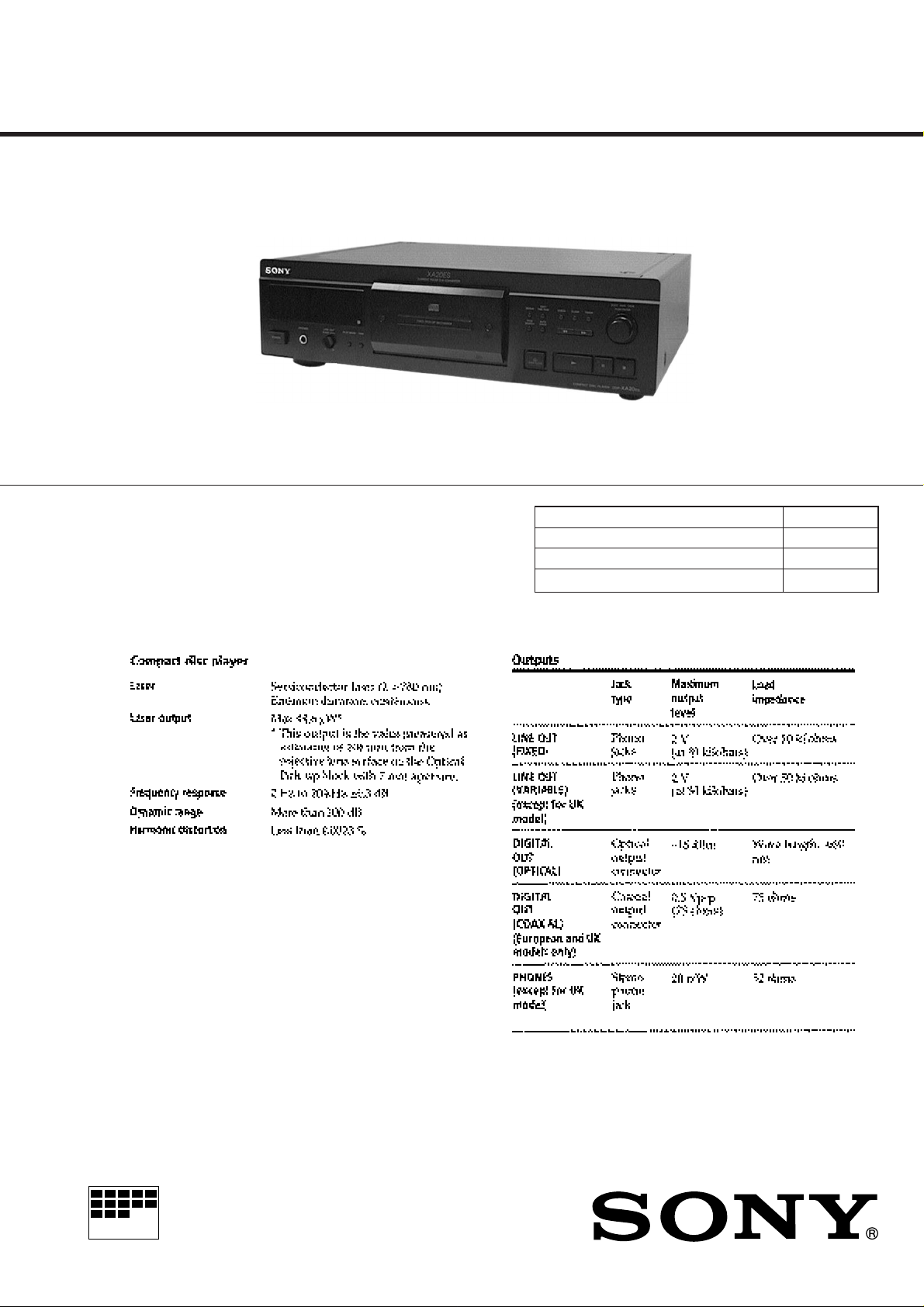
CDP-XA20ES
SERVICE MANUAL
Photo: Black
EXCEPT UK
SPECIFICATIONS
US Model
Canadian Model
AEP Model
UK Model
E Model
Model Name Using Similar Mechanism NEW
CD Mechanism Type
Base Unit Type BU-14C
Optical Pick-up Type KSS-213B
CDM36B-14C
MICROFILM
– Continued on next page –
COMPACT DISC PLAYER
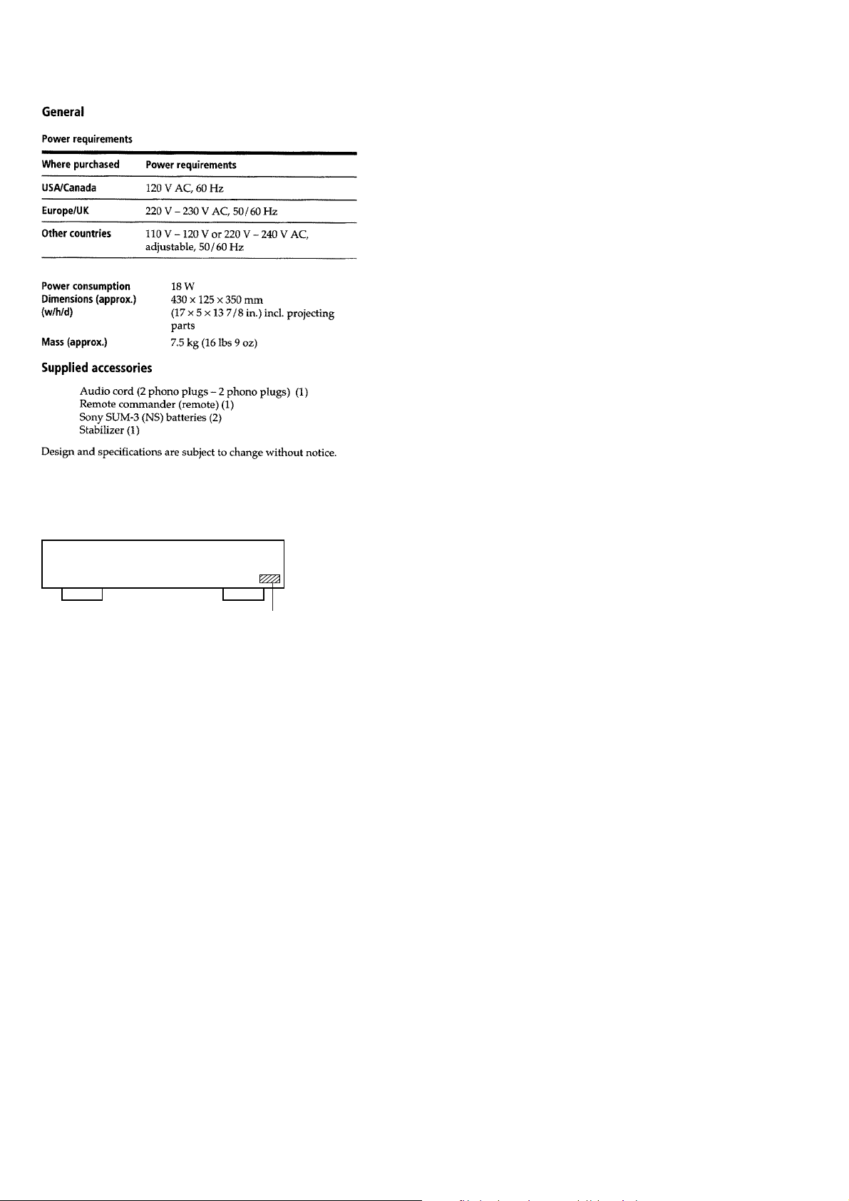
MODEL IDENTIFICATION
– BACK PANEL –
TABLE OF CONTENTS
1. SERVICING NOTES
1-1. How to Open the Disc Tray When Power Switch
Turns Off.......................................................................... 4
1-2. Preparation for Adjustment and Measurement ................ 4
2. GENERAL ................................................................... 5
3. DISASSEMBLY.......................................................... 6
4. TEST MODE
4-1. AF Mode.......................................................................... 11
4-2. ADJ Mode ....................................................................... 12
5. ELECTRICAL ADJUSTMENTS .......................... 13
6. DIAGRAMS
6-1. IC Pin Function Description ............................................ 15
6-2. Block Diagram................................................................. 21
6-3. Printed Wiring Boards –BD Section –............................. 24
6-4. Schematic Diagram — BD Section — ............................ 27
6-5. Schematic Diagram — MAIN Section — ....................... 30
6-6. Printed Wiring Boards — MAIN Section —................... 33
6-7. Schematic Diagram — POWER Section —.................... 35
6-8. Printed Wiring Boards — POWER Section — ............... 37
6-9. Printed Wiring Boards — PANEL Section —................. 39
6-10. Schematic Diagram — PANEL Section — ..................... 41
4-991-138-
AEP Model : 0
UK Model : 1
Singapore Model : 2
US Model : 3
Canadian Model : 4
7. EXPLODED VIEWS ................................................. 47
8. ELECTRICAL PARTS LIST .................................. 52
π
π
π
π
π
SAFETY-RELATED COMPONENT WARNING!!
COMPONENTS IDENTIFIED BY MARK ! OR DOTTED
LINE WITH MARK ! ON THE SCHEMATIC DIAGRAMS
AND IN THE PARTS LIST ARE CRITICAL TO SAFE
OPERATION. REPLACE THESE COMPONENTS WITH
SONY PARTS WHOSE PART NUMBERS APPEAR AS
SHOWN IN THIS MANUAL OR IN SUPPLEMENTS PUBLISHED BY SONY.
ATTENTION AU COMPOSANT AYANT RAPPORT
À LA SÉCURITÉ!
LES COMPOSANTS IDENTIFIÉS P AR UNE MARQUE !
SUR LES DIAGRAMMES SCHÉMATIQUES ET LA LISTE
DES PIÈCES SONT CRITIQUES POUR LA SÉCURITÉ
DE FONCTIONNEMENT. NE REMPLACER CES COMPOSANTS QUE PAR DES PIÈCES SONY DONT LES
NUMÉROS SONT DONNÉS DANS CE MANUEL OU
DANS LES SUPPLÉMENTS PUBLIÉS PAR SONY.
– 2 –
NOTES ON HANDLING THE OPTICAL PICK-UP
BLOCK OR BASE UNIT
The laser diode in the optical pick-up block may suffer electrostatic break-down because of the potential difference generated
by the charged electrostatic load, etc. on clothing and the human
body.
During repair, pay attention to electrostatic break-down and also
use the procedure in the printed matter which is included in the
repair parts.
The flexible board is easily damaged and should be handled with
care.
NOTES ON LASER DIODE EMISSION CHECK
The laser beam on this model is concentrated so as to be focused
on the disc reflective surface by the objective lens in the optical
pick-up block. Therefore, when checking the laser diode emission, observe from more than 30 cm away from the objecti ve lens.
Notes on chip component replacement
• Never reuse a disconnected chip component.
• Notice that the minus side of a tantalum capacitor may be dam-
aged by heat.
SAFETY CHECK-OUT
After correcting the original service problem, perform the following safety check before releasing the set to the customer:
Check the antenna terminals, metal trim, “metallized” knobs,
screws, and all other exposed metal parts for AC leakage. Check
leakage as described below.
LEAKAGE TEST
The AC leakage from any exposed metal part to earth ground and
from all exposed metal parts to any exposed metal part having a
return to chassis, must not exceed 0.5 mA (500 microampers).
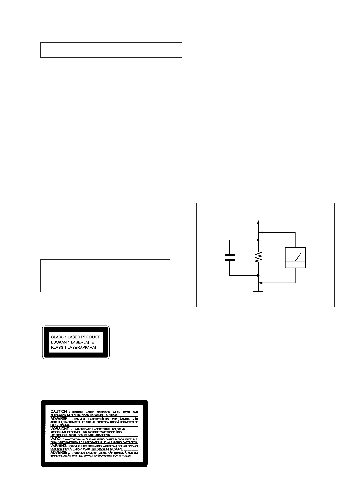
Leakage current can be measured by any one of three methods.
1. A commercial leakage tester, such as the Simpson 229 or RCA
WT -540A. Follow the manuf acturers’ instructions to use these
instruments.
2. A battery-operated AC milliammeter. The Data Precision 245
digital multimeter is suitable for this job.
3. Measuring the voltage drop across a resistor by means of a
VOM or battery-operated AC voltmeter. The “limit” indication is 0.75 V, so analog meters must have an accurate lowvoltage scale. The Simpson 250 and Sanwa SH-63Tr d are examples of a passive VOM that is suitable. Nearly all battery
operated digital multimeters that have a 2 V A C range are suitable. (See Fig. A)
Flexible Circuit Board Repairing
• Keep the temperature of the soldering iron around 270 ˚C dur-
ing repairing.
• Do not touch the soldering iron on the same conductor of the
circuit board (within 3 times).
• Be careful not to apply force on the conductor when soldering
or unsoldering.
CAUTION
Use of controls or adjustments or performance of
procedures other than those specified herein may
result in hazardous radiation exposure.
This appliance is classified as a CLASS 1 LASER product.
The CLASS 1 LASER PRODUCT MARKING is located on
the rear exterior.
Laser component in this product is capable of emitting radiation
exceeding the limit for Class 1.
To Exposed Metal
Parts on Set
AC
0.15 µF
1.5 k
Ω
Earth Ground
voltmeter
(0.75 V)
Fig. A. Using an AC voltmeter to check AC leakage.
The following caution label is located inside the unit.
– 3 –
SECTION 1
SERVICING NOTES
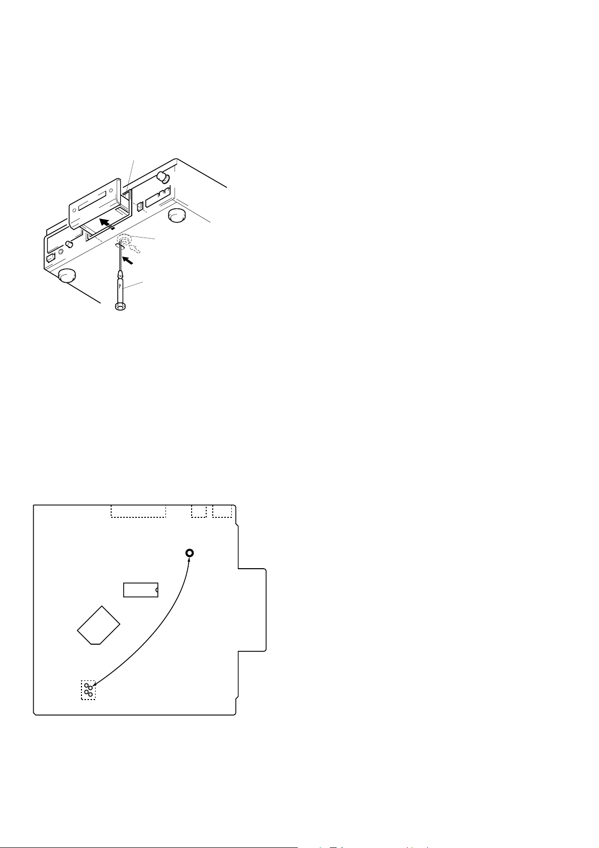
1-1. H OW T O OPEN THE DISC TRAY WHEN
POWER SWITCH TURNS OFF
1 Insert a tapering driver into the aperture of the unit bottom,
and move the limiter (LEVER) to direction of the arrow A.
2 Pull the tray to direction fo the arrow B.
tray
B
Limiter (LEVER)
A
tapering driber
*
To close the disc tray, mo v e the driv er in
the reverse direction (to IN direction).
1-2. PREPARATION FOR ADJUSTMENT AND
MEASUREMENT
Perform connecting the IC361 pin 2 of BD board to the line of
+5V because this unit does not work without the stabilizer structurally.
Connecting Location:
[BD BOARD] – Side B –
CN102
CN103
CN105
TP (VCC)
IC102
IC351
IC361
1
3
2
4
– 4 –
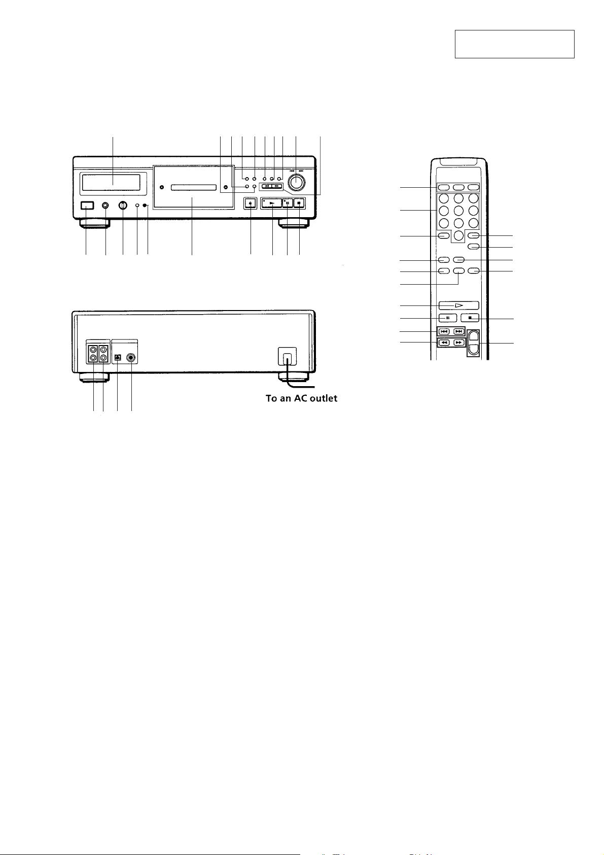
Location of Controls
SECTION 2
GENERAL
This section is extracted
from instruction manual.
• FRONT PANEL
@º
•
•
•
•
•
• REAR PANEL
• REMOTE COMMANDER
!¶ !§!∞!¢!£ !¡!™!•!ª
•
•••
•
•
••
•
••
861 23 54 7 9
•
•
0
@∞
@§
@¶
5
!¶
@ª
8
9
!¡
!™
123
456
789
•
•
10
•
•
•
•••
•
•
•
+
–
!¢
!∞
@•
!£
0
#º
@¡@™ @£ @¢
1 POWER Switch
2 PHONES jack (EXCEPT UK)
3 LINE OUT/PHONE LEVEL control (EXCEPT UK)
4 PLAY MODE button
5 TIME button
6 Disc tray
7 § OPEN/CLOSE button
8 ( (play) button
9 P (pause) button
0 p (stop) button
!¡ 0/) (manual search) buttons
!™ ≠/± ( AMS*) control
!£ FADER button
!¢ CLEAR (program clear) button
!∞ CHECK (program check) button
!§ EDIT/TIME FADE button
!¶ REPEAT button
(CLEAR REPEAT button on the remote commander)
!• PEAK SEARCH button
!ª AUTO SPACE button
@º Display
@¡ LINE OUT FIXED jack
@™ LINE OUT VARIABLE jack (EXCEPT UK)
@£ DIGITAL OUT OPTICAL jack
@¢ DIGITAL OUT COAXIAL jack (AEP, UK)
@∞ Play mode buttons
CONTINUE button
SHUFFLE button
PROGRAM button
@§ Numeric buttons
@¶ >10 (over 10) button
@• DISPLAY ON/OFF button
@ª A˜B button
#º LINE OUT LEVEL +/– buttons
* AMS is the abbreviation of Automatic Music Sensor.
– 5 –
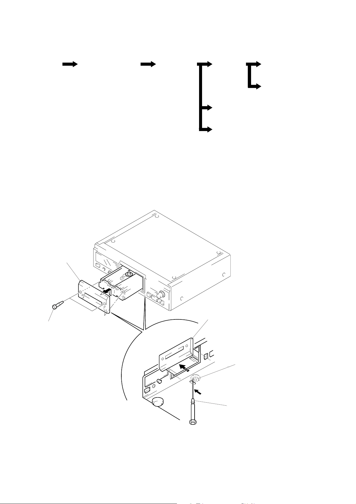
• This set can be disassembled in the order shown below.
SECTION 3
DISASSEMBLY
LOADING PANEL
SECTION
(Page 6)
Note: Follow the disassembly procedure in the numerical order given.
CASE,
FRONT PANEL SECTION
(Page 7)
MECHANISM
DECK SECTION
(Page 7)
LOADING PANEL SECTION
BASE UNIT
(Page 8)
LOADING MOTOR (M103)
(Page 9)
POWER BOARD, MAIN BOARD
(Page 10)
SLED MOTOR (M101)
(Page 8)
OPTICAL PICK-UP
(KSS-213B/S-N)
(Page 9)
4
loading panel section
3
two hexagon hole bolts
(LID)
B
2
Pull the loading panel to
direction of the arrow
A
1
B
.
limiter (LEVER)
Insert a tapering driver,
and move the limiter (LEVER)
to direction of the arrow
A
.
– 6 –
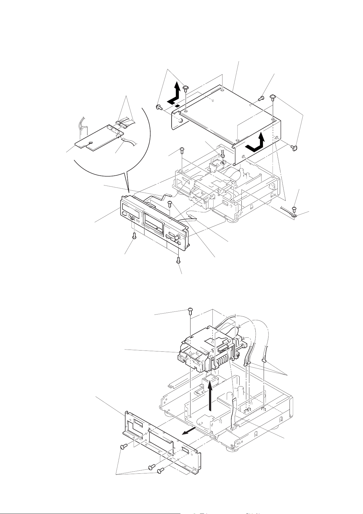
CASE, FRONT PANEL SECTION
8
two connectors
(CN471, 472)
1
four screws
(CASE 3 TP2)
4
connector
(CN992)
3
case
2
screw
(BVTT 3
×
6)
1
four screws
(CASE 3 TP2)
HP board
5
wire (flat type) (11 core)
(CN106)
!£
front panel
7
wire (flat type)
(4 core)
(CN371)
!™
screw (BV 3 × 8)
EXCEPT UK
MECHANISM DECK SECTION
5
!¡
four screws
(BVTT 3
×
two screws
(BVTT 3
!™
6)
×
6)
four screws
(BV 3
×
6)
!¡
two screws
(BVTT 3
6
wire (flat type) (7 core)
(CN107)
×
6)
9
screw
(BVTT 3
0
lug
×
6)
6
mechanism deck
(CDM36B-14C)
4
sub panel
3
six screws
(BVTT 3
1
three connectors
(CN201, 251, 903)
2
wire (flat type) (16 core)
(CN101)
×
6)
– 7 –
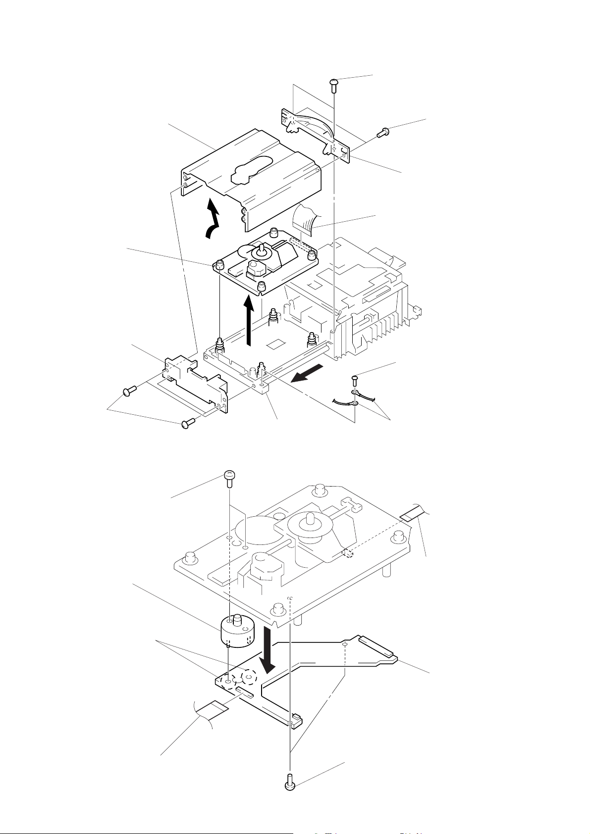
BASE UNIT
3
cover (F) (drawer)
!¡
base unit
(BU-14C)
5
panel (drawer)
4
two screws
(BVTP 3
8
×
8)
6
7
cover (R) (drawer)
wire (flat type) (21 core)
(CN104)
9
screw
(BVTP 3
two screws
(BVTP 3
×
8)
×
8)
2
four screws
(BVTP 3
×
8)
SLED MOTOR (M101)
7
sled motor
(M101)
3
Removal the two solders
of sled motor.
6
two screws
(P1.7
×
2.5)
1
pull the tray
0
two lugs
2
wire (flat type) (5 core)
(CN107)
5
sled board
1
wire (flat type) (16 core)
(CN104)
– 8 –
4
two screws
(BVTP 2.6
×
8)
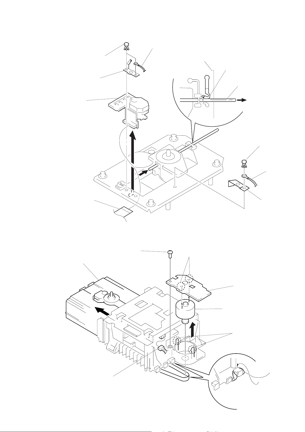
OPTICAL PICK-UP (KSS-213B/S-N)
5
two nylon rivets
7
leaf spring (A) (OP)
0
Removal the optical
pick-up to direction
of the arrow
A
.
A
6
lug
8
claw
9
sled shaft
nylon rivet
2
3
lug
1
wire (flat type) (16 core)
(optical pick-up connector)
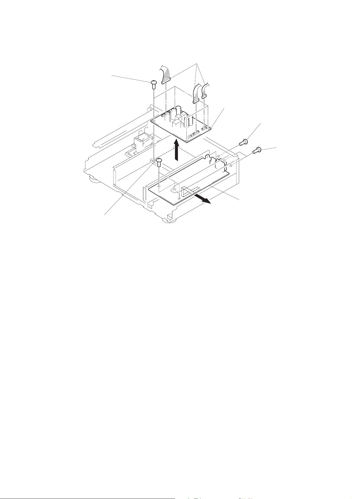
LOADING MOTOR (M103)
1
Pull the tray.
4
screw
(BVTP 3
4
leaf spring
(spindle)
7
×
8)
Remove the two
solders of loading motor.
8
loading motor
(M103)
5
6
loading motor board
two claws
2
connector
(CN103)
– 9 –
3
Hang the belt
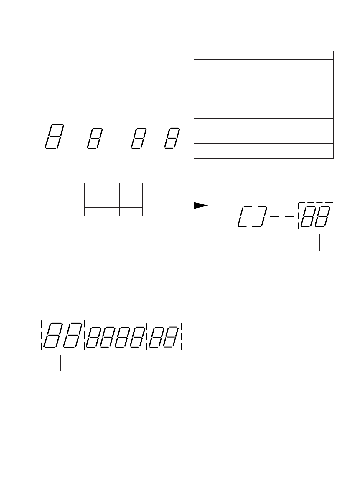
POWER BOARD, MAIN BOARD
2
four screws
(BVTT 3
1
three connectors
(CN901, 902, 951)
×
6)
3
power board
4
screw (BV/RING)
(AEP, UK)
4
two screws
(BV/RING)
6
A
Removal the main board
to direction of the arrow
A
.
5
two screws
(BVTT 3
×
6)
– 10 –
SECTION 4
TEST MODE
4-1. AF MODE
Connect the TP19 (AFADJ) on the BD board to the ground and
turn on the power supply.
The AF mode is then activated and the following check can be
made.
4-1-1. Fluorescent Indicator Tube Check
After confirming display of all on, keep pressing the following
button, and the following display is attained.
” (PLAY) button
(Display: 01)
P (PAUSE) button
24
6810
12 14
16 18 20
(Display: 02)
Table 4-1.
Button Display Button Display
TIME 09
PLAY
MODE TIME FADE
AUTO
SPACE
CHECK 19
CLEAR 20 p 33
FADER 21 ( 01
0 22 P 02
) 23
4-1-3. Remote Commander Check
All buttons are assigned with numbers respectively.
If a button is kept pressed, its button number is displayed on the
FL display tube of main unit. (Table 4-2)
10
18 REPEAT 28
PUSH
ENTER
EDIT/
PEAK
SEARCH
§ all light
OPEN/CLOSE up
24
27
29
A track number on FL display tube increases if = AMS +
knob is rotated in + direction, or decreases in = direction.
Keep pressing the §OPEN/CLOSE button, and all on display is
attained again.
4-1-2. Key Check
All buttons are assigned with numbers respectively , and when each
button is pressed, it is counted and its number is displayed. Up to
“16” can be counted.
A button pressed once is not further counted but the number is
displayed. (Table 4-1)
(
count display button number
display
(
(
button number
display
– 11 –
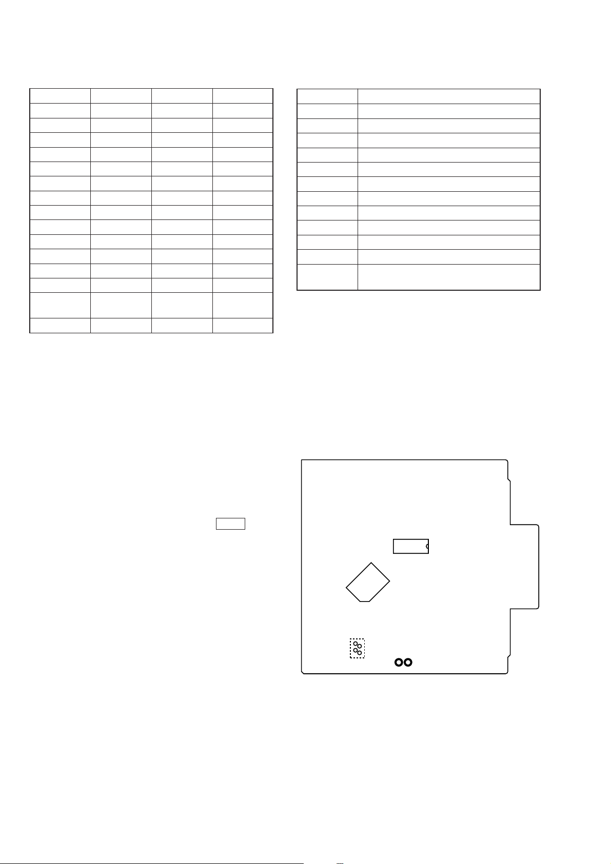
Table 4-2.
Table 4-3.
Button Display Button Display
1 00 10 32
2 01 >10 39
3 02 TIME 40
4 03 A – B 42
5 04 REPEAT 44
6 05 = 48
7 06 + 49
8 07 · 50
9 08 0 51
CHECK 13 ) 52
CLEAR 15 SHUFFLE 53
+ 18 p 56
– 19 P 57
CONTINUE 29
PROGRAM 31 FADER 95
DISPLAY
ON/OFF
86
4-2. ADJ MODE
Connect the TP18 (ADJ) on the BD board to the ground and turn
on the power supply. The ADJ mode is then activated and the
following operation is executed.
• There is no problem even if Guarded Frame Sync is low value
continuously during playing.
• Do not perform high speed search during an access.
• The gain of focus servo and spindle servo does not lo wer during
playing.
• Manual operation and measurement of the servo system are possible. (For detailed operating method, see Table 4-3. in ADJ
Mode.)
Button No. Test Mode
3 Tracking servo off
8 Tracking servo on
11 S-curve measuring mode
12 All servo off
13 Top turnblack display
14 Botton turnblack display
15 Center display
16 Optimum point display
17 Optimum jitter display
18 TE traverse display
19 VC, FE and RF display
20
* For button numbers 3, 8, 11, and 12, use them only when an
oscilloscope is connected.
Autogain display
(Focus, tracking and sled)
4-3. CLV-S MODE
The spindle servo can be operated for play in the CLV-S mode by
connecting TP18 (ADJ) and after turning on the power supply.
4-4. RELEASE THE TEST MODE
Disconnect the lead wire of test point connected in first step.
Connecting Location:
[BD BOARD] – Side B –
4-2-1. Button Operation Table in ADJ Mode
After all music numbers are displayed, press the TIME button,
and the jitter display mode is then set. The button functions are as
listed below.
Button Functions (Operate with remote commander.)
IC351
IC361
TP19 (AFADJ)
IC102
TP18 (ADJ)
– 12 –
SECTION 5
ELECTRICAL ADJUSTMENTS
Notes:
1. CD block basically constructed to operate without adjustment.
Therefore, check each item in order given.
2. Use YEDS-18 disc (Part No.: 3-702-101-01) unless otherwise
indicated.
3. Use the oscilloscope with more than 10 MΩ impedance.
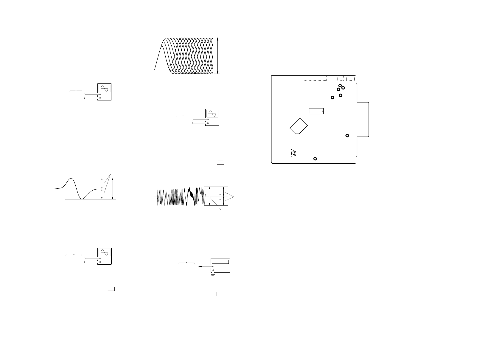
4. Clean an object lens by an applicator with neutral detergent
when the signal level is low than specified value with the following checks.
S-Curve Check
Connection:
BD board
TP2 (FE)
TP (VC)
Procedure:
1. Connect the oscilloscope to TP2 (FE) and TP (VC) on BD
board.
2. Connect the TP3 (FEI: IC101 pin @ª) and TP (VC) with lead
wire.
3. Turned power switch on.
4. Put disc (YEDS-18) in and turned power switch on again and
actuate the focus search. (actuate the focus search when disc
table is moving in and out.)
5. Confirm that the oscilloscope waveform (S-curv e) is symmetrical between A and B. And confirm peak to peak level within
3.0 ± 1.0 Vp-p.
S-curve waveform
6. After check, remove the lead wire connected in step 2.
Note: • Try to measure several times to make sure that the ratio
of A : B or B : A is more than 10 : 7.
• Take sweep time as long as possible and light up the
brightness to obtain best waveform.
RF Level Check
Connection:
BD board
TP1 (RFO)
TP (VC)
Procedure:
1. Connect the oscilloscope to TP1 (RFO) and TP (VC) on BD
board.
2. Turned power switch on. (stop mode)
3. Put disc (YEDS-18) in and press the ( button.
4. Confirm that the oscilloscope waveform is clear and check RF
signal level is correct or not.
Note: Clear RF signal waveform means that the shape “≈” can
be clearly distinguished at the center of the waveform.
oscilloscope
+
–
symmetry
A
B
oscilloscope
(AC range)
+
–
within 3.0 ± 1.0 Vp-p
RF signal waveform
When observing the eye pattern, set the oscilloscope for A C range
and raise vertical sensitivity.
E-F Balance (Traverse) Check
Connection:
BD board
TP4 (TE)
TP (VC)
Procedure:
1. Connect the TP18 (ADJ) to ground and TP5 (TEI: IC101 pin
@¶) to TP (VC)with lead wire.
2. Connect the oscilloscope to TP4 (TE) and TP (VC) on BD
board.
3. Turned power switch on.
4. Put disc (YEDS-18) in and press the ( button.
5. Confirm that the oscilloscope waveform is symmetrical on the
top and bottom in relation to A Vdc, and check this level.
Traverse waveform
×
100 is ± 20 % or less.
A/B
oscilloscope
(DC range)
VOLT/DIV: 200 mV
TIME/DIV: 500 ns
(with the 10: 1 probe
in use)
level: 1.2 Vp-p
+
–
A
B
level: 1.3 ± 0.7 Vp-p
+0.25
–0.20
Symmetry
6. After check, remove the lead wire connected in step 1.
RF PLL Free-run Frequency Check
Connection:
BD board
TP13 (XPLCK)
Procedure:
1. Connect the frequency counter to TP13 (XPLCK).
2. Turned power switch on.
3. Put disc (YEDS-18) in and press the ( button.
4. Confirm that the reading on frequency counter is 4.3218 MHz.
frequency counter
+
–
FOCUS/TRACKING GAIN ADJUSTMENT
VR in optical block is not adjusted.
As this gain has a margin, normally a little shift of gain will not
cause a problem.
If you happened to move VR and you are not sure the original
position, set it to the mechanical center.
Adjustment Location:
[BD BOARD] – Side B –
CN102
TP (VC)
IC102
IC351
IC361
TP4 (TE)
TP2 (FE)
TP18 (ADJ)
CN103
CN105
TP5 (TEI)
TP1 (RFO)
TP13 (XPLCK)
– 13 –
– 14 –
SECTION 6
DIAGRAMS
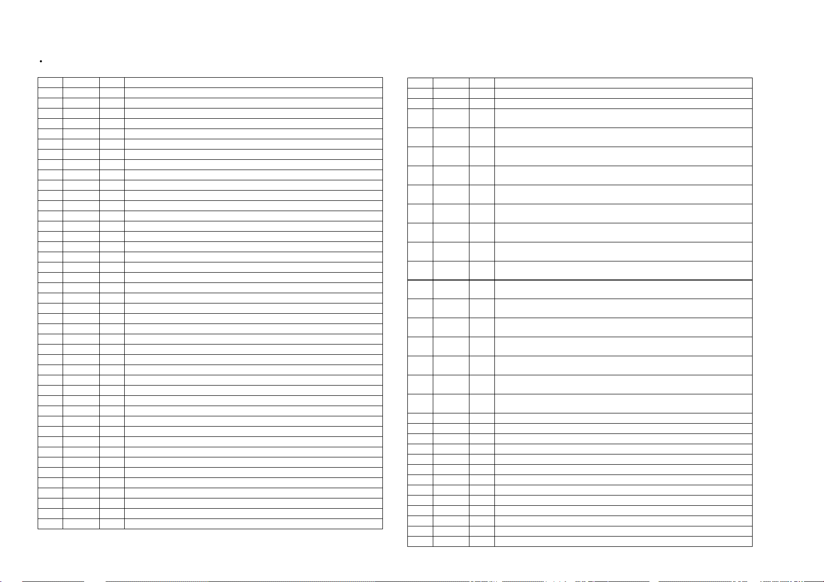
6-1. IC PIN FUNCTION DESCRIPTION
BD BOARD IC101 CXD2545Q
(DIGITAL SIGNAL PROCESSOR, FOCUS/TRACKING/SLED SERVO, EFM COMPARATOR)
Pin No. Pin Name I/O Function
1 SRON O Sled servo drive PWM signal output terminal Not used (open)
2 SRDR O
3 SFON O
4 TFDR O
5 TRON O
6 TRDR O
7 TFON O
8 FFDR O
9 FRON O
10 FRDR O Focus servo drive PWM signal (–) output to the BA6297AFP (IC102)
11
FFON O Focus servo drive PWM signal output terminal Not used (open)
12
VCOO O Oscillator circuit output terminal for analog PLL of the playback EFM Not used (open)
13 VCOI I Oscillator circuit input terminal for analog PLL of the playback EFM Not used (fixed at “L”)
14 TEST I Input terminal for the test (fixed at “L”)
15 DVSS —
16 TES2 I Input terminal for the test (fixed at “L”)
17 TES3 I Input terminal for the test (fixed at “L”)
18 PDO O
19 VPCO O PLL charge-pump output terminal for the variable pitch Not used (open)
20 VCKI I Clock signal input from external VCO for the variable pitch Not used (fixed at “L”)
21
AVD2 — Power supply terminal (+5V) (analog system)
22
IGEN I Power supply terminal (+5V) (for operational amplifier)
23
AVS2 — Ground terminal (analog system)
24
ADIO O Output terminal of the operational amplifier Not used (open)
25
RFC I Input terminal for the A/D converter Not used (open)
26
RFDC I RF signal (DC level) input terminal for the digital servo process
27 TE I
28 SE I Sled error signal input from the RF amplifier in optical pick-up
29
30
31
32
33
34
35
36
37
38
39
40 AVD1 — Power supply terminal (+5V) (analog system)
41 DVDD — Power supply terminal (+5V) (digital system)
42 ASYE I Playback EFM asymmetry circuit on/off selection input terminal (fixed at “H”)
43 PSSL I Audio data output mode selection input terminal (fixed at “L”)
FE I Focus error signal input from the RF amplifier in optical pick-up
VC I Middle point voltage (+2.5V) input from the RF amplifier in optical pick-up
FILO O Filter output terminal for master clock of the playback master PLL
FILI I Filter input terminal for master clock of the playback master PLL
PCO O Phase comparison output terminal for master clock of the playback EFM master PLL
CLTV I Internal VCO control voltage input of the playback master PLL
AVS1 — Ground terminal (analog system)
RFAC I RF signal (AC level) input terminal for the EFM demodulator
BIAS I Constant current input terminal of the playback EFM asymmetry circuit
ASYI I Playback EFM asymmetry comparator voltage input terminal
ASYO O
Sled servo drive PWM signal (–) output to the BA6297AFP (IC102)
Sled servo drive PWM signal output terminal Not used (open)
Tracking servo drive PWM signal (–) output to the BA6297AFP (IC102)
Tracking servo drive PWM signal output terminal Not used (open)
Tracking servo drive PWM signal (+) output to the BA6297AFP (IC102)
Tracking servo drive PWM signal output terminal Not used (open)
Focus servo drive PWM signal (+) output to the BA6297AFP (IC102)
Focus servo drive PWM signal output terminal Not used (open)
Ground terminal (digital system)
Charge-pump output terminal for analog PLL of the playback EFM Not used (open)
Tracking error signal input from the RF amplifier in optical pick-up
Playback EFM full-swing output terminal
Pin No. Pin Name I/O Function
44 WDCK O Word clock signal (88.2 kHz) output terminal Not used (open)
45 LRCK O L/R sampling clock signal (44.1 kHz) output to the CXD8505BQ (IC302)
46 DATA O
47 BCLK O
48 64 DATA O
49 64 BCLK O
50 64 LRCK O
51 GTOP O
52 XUGF O
53 XPLCK O
54 GFS O
55 RFCK O
56 C2PO O
57 XRAOF O
58 MNT3 O
59 MNT2 O
60 MNT1 O
61 MNT0 O
62 XTAI I System clock input terminal (16 MHz)
63 XTAO O System clock output terminal (16 MHz) Not used (open)
64 XTSL I System clock selection input terminal (fixed at “L”)
65 DVSS — Ground terminal (digital system)
66 FSTI I 2/3 divider input terminal of pins ^™ (XATI) and ^£ (XTAO)
67 FSTO O 2/3 divider output terminal of pins ^™ (XATI) and ^£ (XTAO)
68 FSOF O 4.2336 MHz clock signal output terminal Not used (open)
69 C16M O 16.9344 MHz clock signal output terminal Not used (open)
70 MD2 I Digital out on/off control signal input terminal (fixed at “H”)
71 DOUT O Digital signal (for coaxial out and optical out) output terminal
72 EMPH O Emphasis control signal output terminal Not used (open)
73 WFCK O Write frame clock signal output terminal Not used (open)
74 SCOR O Sub-code sync (S0+S1) detection signal output to the system controller (IC351)
DA16 output when PSSL=“H”, 48-bit slot serial data output when PSSL=“L”
(PSSL (pin $£)=fixed at “L”) Serial data output to the CXD8505BQ (IC302)
DA15 output when PSSL=“H”, 48-bit slot bit clock signal output when PSSL=“L”
(PSSL (pin $£)=fixed at “L”) Bit clock signal (2.8224 MHz) output to the CXD8505BQ (IC302)
DA14 output when PSSL=“H”, 64-bit slot serial data output when PSSL=“L”
(PSSL (pin $£)=fixed at “L”) Not used (open)
DA13 output when PSSL=“H”, 64-bit slot bit clock signal output when PSSL=“L”
(PSSL (pin $£)=fixed at “L”) Not used (open)
DA12 output when PSSL=“H”, 64-bit slot L/R sampling clock signal output when PSSL=“L”
(PSSL (pin $£)=fixed at “L”) Not used (open)
DA11 output when PSSL=“H”, GTOP signal output when PSSL=“L”
(PSSL (pin $£)=fixed at “L”) Not used (open)
DA10 output when PSSL=“H”, XUGF signal output when PSSL=“L”
(PSSL (pin $£)=fixed at “L”) Not used (open)
DA09 output when PSSL=“H”, XPLCK signal output when PSSL=“L”
(PSSL (pin $£)=fixed at “L”) Not used (open)
DA08 output when PSSL=“H”, GFS (guard frame sync) signal output when PSSL=“L”
(PSSL (pin $£)=fixed at “L”) Not used (open)
DA07 output when PSSL=“H”, RFCK (read frame clock) signal output when PSSL=“L”
(PSSL (pin $£)=fixed at “L”) Not used (open)
DA06 output when PSSL=“H”, C2PO signal output when PSSL=“L”
(PSSL (pin $£)=fixed at “L”) Not used (open)
DA05 output when PSSL=“H”, XRAOF (RAM over flow) signal output when PSSL=“L”
(PSSL (pin $£)=fixed at “L”) Not used (open)
DA04 output when PSSL=“H”, MNT3 (monitor 3) signal output when PSSL=“L”
(PSSL (pin $£)=fixed at “L”) Not used (open)
DA03 output when PSSL=“H”, MNT2 (monitor 2) signal output when PSSL=“L”
(PSSL (pin $£)=fixed at “L”) Not used (open)
DA02 output when PSSL=“H”, MNT1 (monitor 1) signal output when PSSL=“L”
(PSSL (pin $£)=fixed at “L”) Not used (open)
DA01 output when PSSL=“H”, MNT0 (monitor 0) signal output when PSSL=“L”
(PSSL (pin $£)=fixed at “L”) Not used (open)
– 15 –
– 16 –
 Loading...