


Sipex Corporation SPX8863M5, SPX8863M5-1.8, SPX8863M5-2.5, SPX8863M5-2.8, SPX8863M5-3.0 Datasheet
...
SPX8863
120 mA, Low Dropout Voltage Regulator
(Preliminary Information)
FEATURES |
APPLICATIONS |
||
• Low Noise Output LDO |
• |
PDA |
|
• 1% Initial Accuracy At 120mA |
• |
Battery Powered Systems |
|
• |
Very Low Quiescent Current |
• |
Cellular Phone |
• |
Low Dropout Voltage |
• |
Cordless Telephones |
• Current & Thermal Limiting |
• |
Radio Control Systems |
|
• |
Reverse-Battery Protection |
• |
Portable/Palm Top/Notebook Computers |
• Wide Range of Fix Output Voltages |
• |
Portable Consumer Equipment |
|
|
1.8V, 2.5V, 2.8V, 3.0V, 3.3V, 4.0V, 4.5V, 5.0V, & ADJ |
• |
Portable Instrumentation |
• |
Zero Off-Mode Current |
• |
Bar Code Scanners |
• |
Small 5-Pin SOT-23 |
• |
SMPS Post-Regulator |
•Pin Compatible to MAX8863
PRODUCT DESCRIPTION
The SPX8863 is a low-power positive voltage regulator with ultra low noise output and very low dropout voltage. In addition, this device offers very low quiescent current of approximately 600uA at 100mA output. The SPX8863 initial tolerance is less than 1% max and has a logic compatible ON/OFF switching input. The unique features of the SPX8863 include a reference bypass pin for the best performance results of low noise.
This device is an excellent choice for use in battery powered applications such as cellular/ cordless telephones, radio control systems, and portable computers. When disabled power consumption drops to nearly zero. The device also has a very low output temperature coefficient, making it a low power voltage reference. The SPX8863 key features include protection against reversed battery, fold-back current limiting, and automotive load dump protection.
The SPX8863 is available in many fixed voltages (1.8V, 2.5V, 2.8V, 3.0V, 3.3V, 4.0V, 4.5V, & 5.0V) or with an adjustable output. This device is offered in a small 5-pin SOT-23 package, providing a small footprint with all the performance features with fixed or adjustable output.
MARKING INFORMATION |
|
|
|
|
|
|
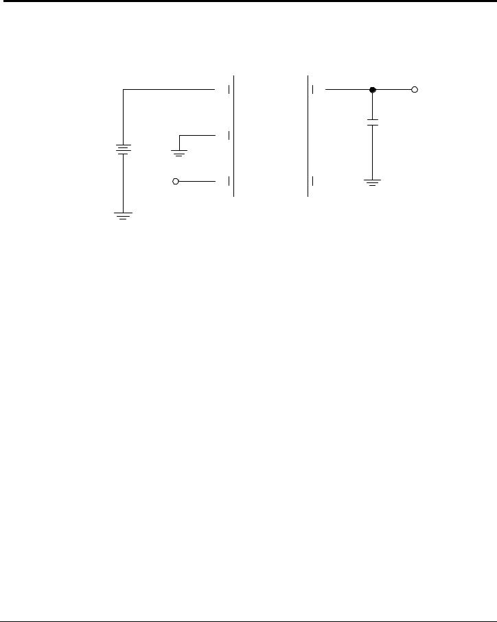
PIN CONNECTIONS |
|
|
|
|
|||||||||||
Voltage |
Marking |
Voltage |
Marking |
|
|
|
|
|
|
|
|
|
||||||||||
|
SOT-23-5 (M5) |
|
SOT-23-5 (M5) |
|||||||||||||||||||
|
|
|
|
|
|
|||||||||||||||||
1.8 |
9WXX |
4.5 |
A4XX |
|
BYP |
|
VOUT |
|
ADJ |
|
|
VOUT |
||||||||||
2.5 |
9XXX |
4.70 |
A5XX |
|
|
|
||||||||||||||||
|
|
|
|
|
|
|
|
|
|
|
|
|
|
|
|
|
|
|
||||
|
|
|
|
|
|
|
|
|
|
|
|
|
|
|
|
|
|
|
|
|
|
|
2.8 |
9YXX |
5.0 |
A6XX |
|
|
|
|
|
|
|
|
|
|
|
|
|
|
|
|
|
|
|
|
5 |
|
|
4 |
|
|
|
5 |
|
|
|
4 |
|
|
||||||||
3.0 |
A3XX |
ADJ |
A7XX |
|
|
|
|
|
|
|
|
|
|
|
||||||||
|
|
SPX8863 |
|
|
|
SPX8863 |
|
|||||||||||||||
3.3 |
A2XX |
|
|
|
|
|
|
|
|
|||||||||||||
|
|
|
1 |
|
2 |
3 |
|
|
|
1 |
|
2 |
|
3 |
|
|
||||||
|
|
|
|
|
|
|
|
|
|
|
|
|
||||||||||
|
|
|
|
|
|
|
|
|
|
|
|
|
|
|
|
|
|
|
|
|
|
|
|
|
|
|
|
|
|
|
|
|
|
|
|
|
|
|
|
|
|
|
|
|
|
|
|
|
|
|
|
EN GND |
VIN |
|
EN GND VIN |
|||||||||||||
|
|
|
|
|
|
Top View |
|
|
Top View |
|||||||||||||
|
|
|
|
Fixed Output Voltage |
Adjustable Output Voltage |
|||||||||||||||||
Rev. 10/24/00

SPX8863
ABSOLUTE MAXIMUM RATINGS
Power Dissipation...................................... |
Internally Limited |
Lead Temp. (Soldering, 5 Seconds) ............................ |
260°C |
Operating Junction Temperature Range ..... |
-40°C to +125°C |
Input Supply Voltage........................................ |
-20V to +20V |
Enable Input Voltage........................................ |
-20V to +20V |
RECOMMENDED OPERATING CONDITIONS
Input Voltage.................................................. |
+2.5V to+16V |
Operating Junction Temperature Range ..... |
-40°C to +125°C |
Enable Input Voltage............................................. |
0V to VIN |
SOT-23-5 (θJA) ..................................................... |
See Note 1 |
ELECTRICAL CHARACTERISTICS
TJ = 25°C, VIN = VOUT + 1V, IL = 100µA, CL = 1.0µF, and VENABLE > 2.4V. Unless otherwise specified boldface applies over the junction temperature range
Parameter |
Test Conditions |
Typ |
Min |
Max |
Units |
|
|
|
|
|
|
Output Voltage Tolerance (VOUT) |
IL = 100µA |
|
-1 |
+1 |
%VNOM |
|
IL = 500µA |
|
-2 |
+2 |
|
Output Voltage Temperature Coef |
|
40 |
|
|
ppm/°C |
Line Regulation |
VIN = VOUT + 1V to 16V |
0.03 |
|
0.1 |
%/V |
|
VIN = VOUT + 1V to 16V |
|
|
0.2 |
|
Load Regulation |
IL = 0.1mA to 120mA |
0.1 |
|
0.2 |
% |
|
IL = 0.1mA to 120mA |
|
|
0.5 |
|
Dropout Voltage (See Note 2) |
IL = 100 µA |
30 |
|
50 |
mV |
(VIN- VO) |
IL = 50mA |
140 |
|
190 |
|
|
|
||||
|
IL = 120mA |
190 |
|
260 |
|
Quiescent Current (IGND) |
VENABLE < 0.6V |
< 1 |
|
1 |
µA |
|
VENABLE < 0.25V |
|
|
5 |
|
|
|
|
|
||
Ground Pin Current |
IL = 100 µA |
80 |
|
125 |
µA |
(IGND) |
IL = 50 mA |
350 |
|
600 |
|
|
|
||||
|
IL = 120mA |
950 |
|
1600 |
|
Ripple Rejection (PSRR) |
|
55 |
|
|
dB |
Current Limit (ILIMIT) |
VOUT = 0V |
360 |
320 |
|
mA |
Output Noise (eNO) |
IL = 50mA, CL = 1.0µF |
390 |
|
|
µVRMS |
|
(10Hz – 100KHz) |
|
|
|
|
Input Voltage Level |
|
|
|
|
|
Logic Low (VIL) |
OFF |
|
|
0.6 |
V |
Input Voltage Level |
|
|
|
|
|
|
|
|
|
|
|
Logic High (VIH) |
ON |
|
2.0 |
|
|
ENABLE Input Current |
VIL < 0.6V |
0.01 |
|
2 |
µA |
|
VIH > 2.0V |
2 |
|
20 |
|
|
|
|
|
|
|
Note 1: The maximum allowable power dissipation is a function of maximum operating junction temperature, TJ (max), the junction to ambient thermal resistance, and the ambient, θJA, and the ambient temperature TA. The maximum allowable power dissipation at any ambient temperature is given:
PD (max) = (TJ(max) - TA) θJA. Exceeding the maximum allowable power limit will result in excessive die temperature; thus, the regulator will go into thermal shutdown. The θJA of the SPX8863 is 220oC/W mounted on a PC board.
Note 2: Not apply to 1.8V version.
Rev. 10/24/00
SPX8863
TYPICAL APPLICATION
3 |
|
|
|
4 |
|
|
VIN |
|
|
|
|
|
VOUT |
|
|
|
|
|
||
|
2 |
+ |
1.0uF |
||||
GND |
|
SPX8863 |
|||||
|
|
||||||
+ |
|
|
|
|
|
|
|
EN |
1 |
5 |
BYP |
|
|||
|
|
|
|
|
|
||
|
|
|
|
|
|
||
|
|
|
|
|
|
(Optn) |
|
|
|
|
|
|
|
|
|
|
|
|
|
|
|
|
|
|
ENABLE may be tied directly to VIN |
|
|||||
Rev. 10/24/00
 Loading...