


SP690RCN
Sipex Corporation SP690RCN, SP690RCP, SP690REN, SP690REP, SP690SCN Datasheet
...
1
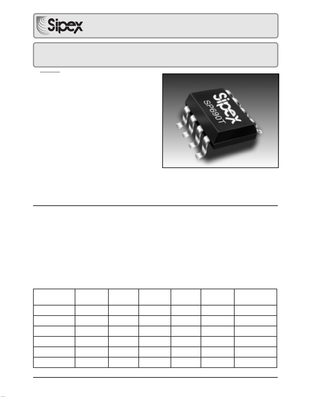
SP690T/S/R DS/10 SP690T/S/R, 802/T/S/R, 804T/S/R, 805T/S/R Low Power Microprocessor Supervisory © Copyright 2000 Sipex Corporation
SP690T/S/R, SP802T/S/R,
SP804T/S/R, and SP805T/S/R
3.0V/3.3V Low P o wer Micropr ocessor
Supervisory with Battery Switch-Over
The SP690T/S/R, SP802T/S/R, SP804T/S/R and SP805T/S/R devices are a family of
microprocessor (µP) supervisory circuits that integrate a myriad of components involved in
discrete solutions to monitor power-supply and battery-control functions in µP and digital
systems. The series will significantly improve system reliability and operational efficiency
when compared to discrete solutions. The features of the SP690T/S/R, SP802T/S/R,
SP804T/S/R and SP805T/S/R devices include a watchdog timer, a µP reset and backup-
battery switchover, and power-failure warning; a complete µP monitoring and watchdog
solution. The series is ideal for 3.0V or 3.3V applications in portable electronics, computers,
controllers, and intelligent instruments and is a solid match for designs where it is critical to
monitor the power supply to the µP and it’s related digital components. Refer to Sipex's
SP690A/692A/802L/802M/805L/805M series for similar devices designed for +5V systems.
■ RESET and RESET Outputs
■ Reset asserted down to V
CC
= 1V
■ Reset Time Delay - 200ms
■ Watchdog Timer - 1.6 sec timeout
■ 40µA Maximum V
CC
Supply Current
■ 1µA Maximum Battery Supply Current
■ Power Switching
50mA Output in V
CC
Mode (1.5Ω)
10mA Output in Battery Mode (15Ω)
■ Battery Can Exceed V
CC
in Normal Operation
■ Precision Voltage Monitor for Power-Fail
or Low-Battery Warning
■ Available in 8 pin SO and DIP packages
■ Pin Compatible Upgrades to
MAX690T/S/R, MAX802T/S/R,
MAX804T/S/R, MAX805T/S/R
DESCRIPTION
rebmuNtraP
TESER
evitcAevitcA
evitcA
evitcAevitcA
TESER
dlohserhTdlohserhT
dlohserhT
dlohserhTdlohserhT
TESER
ycaruccAycaruccA
ycaruccA
ycaruccAycaruccA
IFP
ycaruccAycaruccA
ycaruccA
ycaruccAycaruccA
godhctaW
tupnItupnI
tupnI
tupnItupnI
yrettaB-pukcaB
hctiwShctiwS
hctiwS
hctiwShctiwS
T508/T096PSHGIH/WOLV570.3Vm57±%4±SEYSEY
T408/T208PSHGIH/WOLV570.3Vm06±%2±SEYSEY
S508/S096PSHGIH/WOLV529.2Vm57±%4±SEYSEY
S408/S208PSHGIH/WOLV529.2Vm06±%2±SEYSEY
R508/R096PSHGIH/WOLV526.2Vm57±%4±SEYSEY
R408/R208PSHGIH/WOLV526.2Vm06±%2±SEYSEY
®
SP690T/S/R DS/10 SP690T/S/R, 802/T/S/R, 804T/S/R, 805T/S/R Low Power Microprocessor Supervisory © Copyright 2000 Sipex Corporation
2
ABSOLUTE MAXIMUM RATINGS
These are stress ratings only and functional operation of the device at
these ratings or any other above those indicated in the operation
sections of the specifications below is not implied. Exposure to absolute
maximum rating conditions for extended periods of time may affect
reliability and cause permanent damage to the device.
V
CC
..................................................................................-0.3V to 6.0V
V
BATT
................................................................................-0.3V to 6.0V
All Other Inputs (NOTE 1).................................-0.3V to the higher of V
CC
or V
BATT
Continuous Input Current:
V
CC
..................................................................................100mA
V
BATT
..................................................................................20mA
GND..................................................................................20mA
WDI, PFI...........................................................................20mA
Continuous Output Current:
RESET, RESET, PFO.........................................................20mA
V
OUT
......................................................................................100mA
Power Dissipation per Package:
8pin NSOIC (derate 6.14mW/°C above +70°C)..............500mW
8pin PDIP (derate 11.8mW/°C above +70°C)..............1,000mW
Storage Temperature........................................-65°C to +160°C
Lead Temperature(soldering,10sec).............................................+300°C
ESD Rating........................................................4KV Human Body Model
SPECIFICATIONS
V
CC
= 3.17V to 5.50V for the SP690T/SP80_T, V
CC
= 3.02V to 5.50V for the SP690S/SP80_S, V
CC
= 2.72V to 5.50V for the SP690R/SP80_R, V
BATT
= 3.60V, and
T
A
= T
MIN
to T
MAX
unless otherwise noted. Typical values taken at T
AMB
= +25
O
C.
SRETEMARAP.NIM.PYT.XAMSTINUSNOITIDNOC
,egnaRegatloVgnitarepO0.15.5stloV
V
CC
Vro
YRETTAB
,ETON1
V
CC
I,tnerruCylppuS
YLPPUS
5204
µA
Ignidulcxe
TUO
V
CC
yrettaBnitnerruCylppuS
edoMpukcaB
0204
µA
V
CC
V,V0.2=
YRETTAB
,V3.2=
Ignidulcxe
TUO
V
YRETTAB
nitnerruCylppuS
,edoMynAETON2
4.01
µA
Ignidulcxe
TUO
V
YRETTAB
ETON,tnerruCegakaeL3
100.05.0
µA
V
YRETTAB
ETON,tnerruCegakaeL41.0-
20.0
µA
V>V3.3
CC
V>
YRETTAB
V2.0+
V,egatloVtuptuO
TUO
V
CC
30.0-
V
CC
3.0-
V
CC
5100.0-
V
CC
5700.0-
V
CC
570.0-
V
CC
3000.0-
V
Am5=I
I
TUO
Am05=
I
TUO
052=µV,A
CC
V5.2>
V
TUO
edoMpukcaB-yrettaBniV
YRETTAB
20.0-V
YRETTAB
5400.0-
V
YRETTAB
810.0-
V
YRETTAB
51.0-
V
I
TUO
V,Aµ052=
YRETTAB
V3.2=
I
TUO
V,Am1=
YRETTAB
V3.2=
I
TUO
BV,Am01=
YRETTA
V3.3=
,dlohserhThctiwSyrettaB
V
CC
gnillaf
560.0
03.2
520.0
04.205.2
V
V
YRETTAB
V-
CC
V,
WS
V>
CC
5ETON,V57.1>
V
YRETTAB
V>
CC
6ETON,
,dlohserhThctiwSyrettaB
V
CC
7ETON,gnisir
V
teseRehtotlacitnedieraseulaV
VtaseulavdlohserhT
CC
gnisir
3
SP690T/S/R DS/10 SP690T/S/R, 802/T/S/R, 804T/S/R, 805T/S/R Low Power Microprocessor Supervisory © Copyright 2000 Sipex Corporation
SRETEMARAP.NIM.PYT.XAMSTINUSNOITIDNOC
V,dlohserhTteseR
TSR
8ETON
00.3
00.3
58.2
58.2
55.2
55.2
570.3
580.3
529.2
539.2
526.2
536.2
51.3
71.3
00.3
20.3
07.2
27.2
V
V,T508/T096PS
CC
gnillaf
V,T508/T096PS
CC
gnisir
V,S508/S096PS
CC
gnillaf
V,S508/S096PS
CC
gnisir
V,R508/R096PS
CC
gnillaf
V,R508/R096PS
CC
gnisir
00.3
00.3
88.2
88.2
95.2
95.2
570.3
580.3
529.2
539.2
526.2
536.2
21.3
41.3
00.3
20.3
07.2
27.2
V
V,T408/T208PS
CC
gnillaf
V,T408/T208PS
CC
gnisir
V,S408/S208PS
CC
gnillaf
V,S408/S208PS
CC
gnisir
V,R408/R208PS
CC
gnillaf
V,R408/R208PS
CC
gnisir
teseRt,doirePtuoemiT
PW
041002082sm
V,egatloVtuptuOOFP,TESER
HO
V
CC
3.0-V
CC
51.0-VI
ECRUOS
Aµ03=
V,egatloVtuptuOOFP,TESER
LO
60.003.0V
I
KNIS
erehw_208/_096PS,Am2.1=
V
CC
V=
TSR
muminim
V,egatloVtuptuOOFP,TESER
LO
31.003.0VV
YRETTAB
V,V0=
CC
I,V0.1=
KNIS
Aµ04=
V,egatloVtuptuOTESER
LO
60.003.0V
I
KNIS
erehw_508/_408PS,Am2.1=
V
CC
V=
TSR
mumixam
,tnerruCegakaeLtuptuOTESER
11ETON
1-1-
µA
V
YRETTAB
V,V0=
CC
V=
TSR
,muminim
V
TESER
VroV0=
CC
I,tnerruCDNGottrohStuptuO
SO
,
TESERdnaOFP
081005
µA
V
CC
V,V3.3=
HO
V0=
t,tuoemiTgodhctaW
DW
21.106.142.2sV
CC
V6.3<
htdiWesluPIDW00204sn
dlohserhTtupnIIDW
V
HI
V
LI
Vx3.0
CC
Vx7.0
CC
V
tnerruCtupnIIDW1-10.01
µA
V<V0
CC
V5.5<
dlohserhTtupnIIFP002.1
522.1
52.1
52.1
003.1
572.1
V
V,_508/_096PS
CC
<V,V6.3
IFP
gnillaf
V,_408/_208PS
CC
<V,V6.3
IFP
gnillaf
tnerruCtupnIIFP52-10.052An
V,siseretsyHIFP
HFP
0102VmV,gnisirIFP
CC
<V6.3
SPECIFICATIONS (continued)
V
CC
= 3.17V to 5.50V for the SP690T/SP80_T, V
CC
= 3.02V to 5.50V for the SP690S/SP80_S, V
CC
= 2.72V to 5.50V for the SP690R/SP80_R, V
BATT
= 3.60V, and
T
A
= T
MIN
to T
MAX
unless otherwise noted. Typical values taken at T
AMB
= +25
O
C.

SP690T/S/R DS/10 SP690T/S/R, 802/T/S/R, 804T/S/R, 805T/S/R Low Power Microprocessor Supervisory © Copyright 2000 Sipex Corporation
4
SPECIFICATIONS (continued)
V
CC
= 3.17V to 5.50V for the SP690T/SP80_T, V
CC
= 3.02V to 5.50V for the SP690S/SP80_S, V
CC
= 2.72V to 5.50V for the SP690R/SP80_R, V
BATT
= 3.60V, and
T
A
= T
MIN
to T
MAX
unless otherwise noted. Typical values taken at T
AMB
= +25
O
C.
NOTE 1: The following are tested at V
BATT
= 3.6V and V
CC
= 5.5V: V
CC
supply current, watchdog
functionality, logic input leakage, PFI functionality, and the RESET and RESET states. The state of
RESET or RESET and PFO is tested at V
CC
= V
CC
(min).
NOTE 2: Tested V
BATT
= 3.6V, V
CC
= 3.5V and 0V.
NOTE 3: Leakage current into the battery is tested under the following worst-case conditions: V
CC
= 5.5V, V
BATT
= 1.8V and at V
CC
= 1.5V, V
BATT
= 1.0V.
NOTE 4: "-" equals the battery-charging current, "+" equals the battery-discharging current.
NOTE 5: When V
SW
> V
CC
> V
BATT
, V
OUT
remains connected to V
CC
until V
CC
drops below V
BATT
. The
V
CC
-to-V
BATT
comparator has a small 25mV typical hysteresis to prevent oscillation.
NOTE 6: When V
BATT
> V
CC
> V
SW
, V
OUT
remains connected to V
CC
until V
CC
drops below the battery
switch threshold, V
SW
.
NOTE 7: V
OUT
switches from V
BATT
to V
CC
when V
CC
rises above the reset threshold, independent of
V
BATT
. Switchover back to V
CC
occurs at the exact voltage that causes RESET to go HIGH (on the
SP804_ and SP805_ RESET goes LOW). Switchover occurs 200ms prior to reset.
NOTE 8: The reset threshold tolerance is wider for V
CC
rising than for V
CC
falling to accommodate the
10mV typical hysteresis, which prevents internal oscillation.
NOTE 9: SP690_ and SP802_ devices only.
NOTE 10: SP804_ and SP805_ devices only.
NOTE 11: The leakage current into or out of the RESET pin is tested with RESET asserted (RESET
output high impedance).
5
SP690T/S/R DS/10 SP690T/S/R, 802/T/S/R, 804T/S/R, 805T/S/R Low Power Microprocessor Supervisory © Copyright 2000 Sipex Corporation
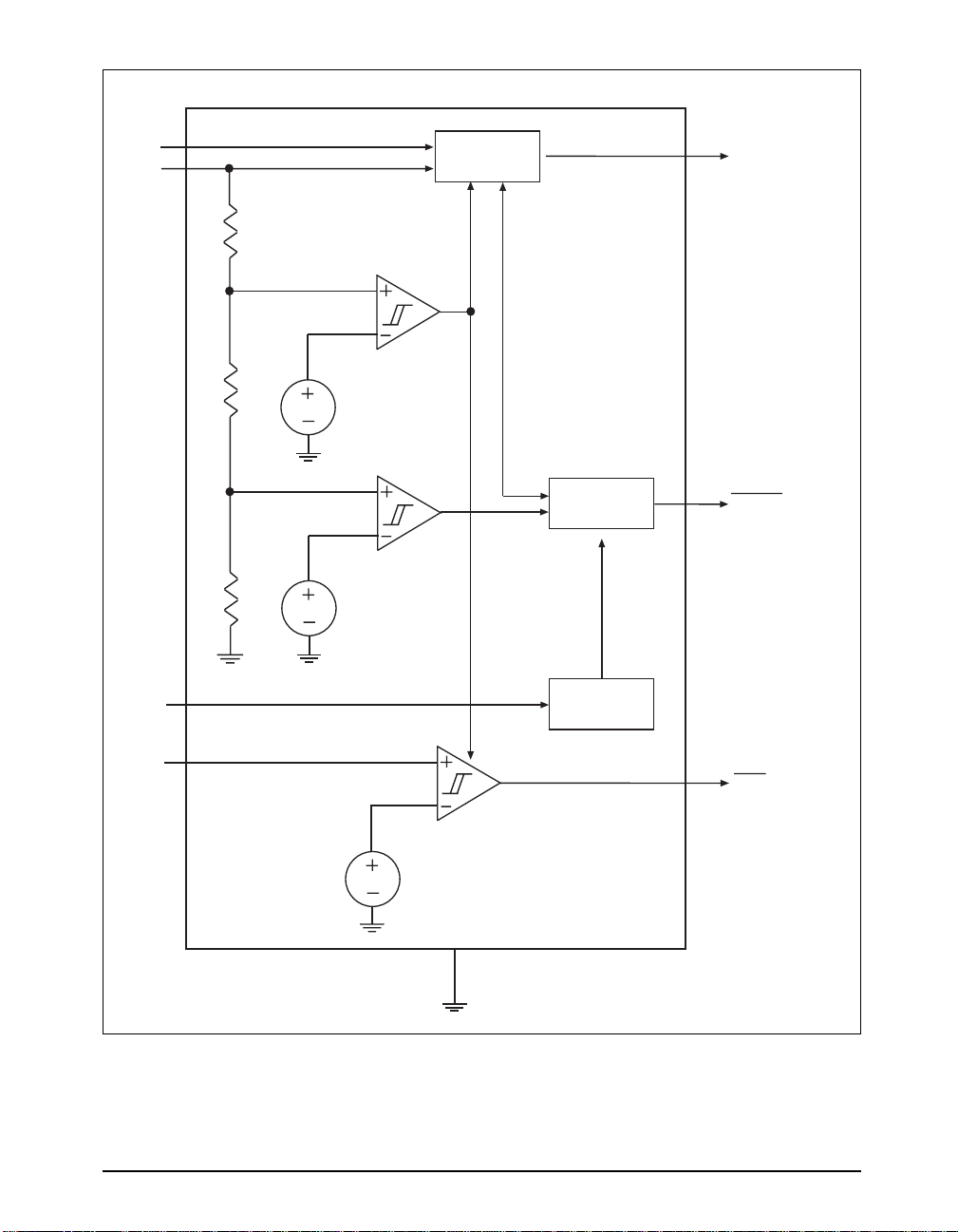
INTERNAL BLOCK DIAGRAM
1.25V
BATTERY
SWITCHOVER
CIRCUIT
PFI
WATCHDOG
TIMER
RESET
GENERATOR
V
CC
BATTERY
SWITCHOVER
COMPARATOR
RESET
COMPARATOR
1.25V
1.25V
WDI
V
BATT
PFO
RESET / RESET*
SP690T/S/R
SP802T/S/R
SP804T/S/R
SP805T/S/R
*SP804T/S/R and SP805T/S/R only
POWER-FAIL
COMPARATOR
7
5
4
6
8
2
V
OUT
GND
3
1
SP690T/S/R DS/10 SP690T/S/R, 802/T/S/R, 804T/S/R, 805T/S/R Low Power Microprocessor Supervisory © Copyright 2000 Sipex Corporation
6
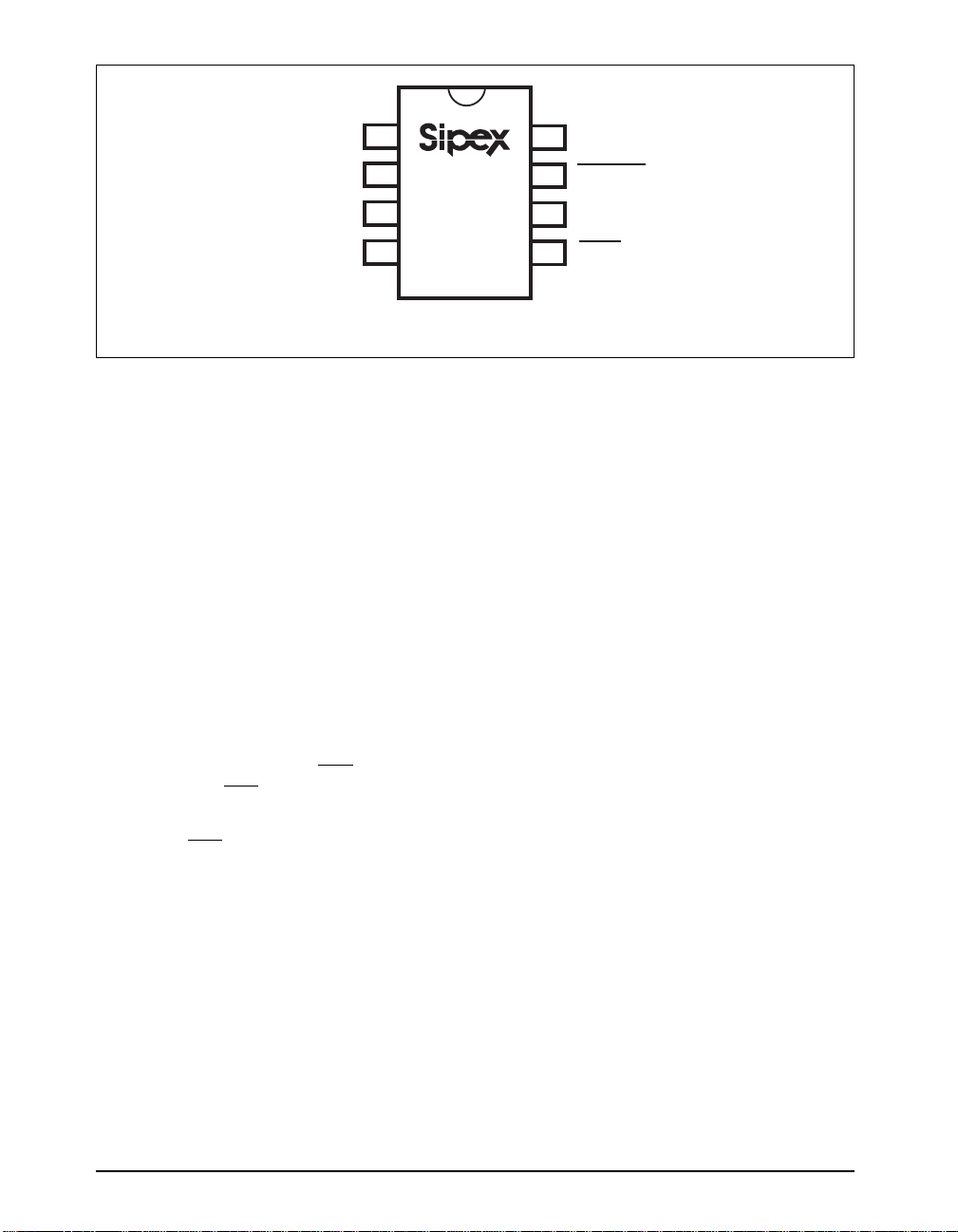
PIN ASSIGNMENTS
Pin 1 —V
OUT
— Output Supply Voltage for
CMOS RAM. When V
CC
is above the
reset threshold, V
OUT
connects to V
CC
through a P-channel MOSFET switch.
When V
CC
falls below the V
SW
and
V
BATTERY
, V
BATTERY
connects to V
OUT
.
Connect to V
CC
if no battery is used.
Pin 2 — V
CC
— +5V Supply Input
Pin 3 — GND — Ground reference for all
signals
Pin 4 — PFI — Power-Fail Comparator Input.
When PFI is less than 1.25V or when V
CC
falls below the V
SW
, PFO goes LOW,
otherwise PFO remains HIGH. Connect
to GND if unused.
Pin 5 — PFO — Power-Fail Comparator
Output. Leave open if unused.
Pin 6 — WDI — Watchdog Input. If WDI
remains HIGH or LOW for 1.6 seconds,
the internal watchdog timer triggers a
reset. The internal watchdog timer clears
when reset is asserted or WDI sees a
rising or falling edge. The watchdog
function cannot be disabled.
Pin 7 for SP690_/802_ only — Active-LOW
Reset Output. — Whenever RESET is
triggered by a watchdog timeout, it goes
LOW for 200ms. It stays LOW whenever
V
CC
is below the reset threshold and re-
mains LOW for 200ms after V
CC
rises
above the reset threshold or when the
watchdog triggers a reset.
Pin 7 for SP804_/805_ only — Active-HIGH
Open-Drain Reset Output. — The
inverse operation of RESET.
Pin 8 — V
BATTERY
— Backup-Battery Input.
When V
CC
falls below V
SW
and V
BATTERY
,
V
OUT
switchesfrom V
CC
to V
BATTERY
.
When V
CC
rises above the reset threshold,
V
OUT
reconnects to V
CC
. V
BATTERY
may
exceed V
CC
. Connect to V
CC
if no battery
is used.
V
OUT
V
CC
GND
PFI
V
BATTERY
RESET / RESET*
WDI
PFO
1
2
3
4
5
6
7
8
*SP804T/S/R and SP805T/S/R only
SP690T/S/R
SP802T/S/R
SP804T/S/R
SP805T/S/R
PINOUT
 Loading...