


Sipex Corporation SPX2954AM3-3.3, SPX2954AM3-5.0, SPX2954AN-3.3, SPX2954AN-5.0, SPX2954M3-3.3 Datasheet
...
SPX2954
|
250 mA Low Drop Out Voltage Regulator |
FEATURES |
APPLICATIONS |
• Output Accuracy 5V, 3.3V,@ 250mA Output |
• Battery Powered Systems |
• Very Low Quiescent Current |
• Cordless Telephones |
• Low Dropout Voltage |
• Radio Control Systems |
• Extremely Tight Load And Line Regulation |
• Portable/Palm Top/Notebook Computers |
• Very Low Temperature Coefficient |
• Portable Consumer Equipment |
• Current & Thermal Limiting |
• Portable Instrumentation |
• Improved Replacement With Hight IOUT For LP2954 Sockets |
• Automotive Electronics |
|
• SMPS Post-Regulator |
SPX2954 Version Over LP2954 |
• Voltage Reference |
• Error Flag Warns Of Output Dropout |
• Avionics |
•Logic-Controlled Electronic Shutdown
•Output Programmable From 1.24V to 29V
•Input Can Withstand -20V Reverse Battery & +60 Positive Transient
PRODUCT DESCRIPTION
The SPX2954 is a low power voltage regulator. This device is an excellent choice for use in battery-powered applications such as cordless telephones, radio control systems, and portable computers. The SPX2954 features very low quiescent current (75 A Typ.) and very low dropout voltage. This includes a tight initial tolerance of ± 0.5% max and ± 1% max., and very low output temperature coefficient, making the SPX2954 useful as a low-power voltage reference. The key SPX2954 features include protection against reversed battery, fold-back current limiting, and automotive load dump protection (60V positive transient).
The error flag output feature is used as power-on reset for warning of a low output voltage, due to falling voltage input of batteries. Another feature is the logic compatible shutdown input which enables the regulator to be switched on and off. The SPX2954 is offered in a 3-pin TO-92and TO-263 package compatible with other 5 volt regulators, in 8-Pin plastic, SO-8, (same pin out as SPX2951), TO220 and TO-263.
The regulator output voltage (of the 8-pin) may be pin-strapped for a 5Vand 3.3V or programmed from 1.24V to 29V with an external pair of resistors. Look for SPX2951 for 150mA and LP2951 for 100mA applications.
PIN CONNECTIONS
TO-263-3 Package |
TO-263-5 Package |
8-Pin Surface Mount (S) |
SOT-223 Package |
TO-220-3 Package TO-220-5 Package |
|
|
|
|
|
|
|
|
|
OUTPUT |
1 |
|
8 |
INPUT |
|
|
|
|
|
|
|
|
|
|
|
SPX2954 |
|
|
SPX2954 |
|
|
SENSE |
2 |
|
7 |
FEEDBACK |
SPX2954 |
|
|
|
|
|
|
|
||||
|
|
|
|
|
|
SPX2954 |
|
|
|
|
|
|
|
|
|
||||||||
1 |
2 |
3 |
1 |
2 |
3 |
4 |
5 |
1) INPUT |
SHUTDOWN |
3 |
|
6 |
5V, 3.3V TAP |
1 |
2 |
3 |
SPX2954 |
SPX2954 |
|||||
GND |
4 |
|
5 |
ERROR |
|
|
|
|
|
|
|
|
|
1) INPUT |
|||||||||
|
|
|
|
|
|
|
|
2) OUTPUT |
|
|
|
|
|
|
|
|
|
|
|||||
|
|
|
|
|
|
|
|
|
|
|
|
|
|
|
|
|
|
2) OUTPUT |
|||||
|
|
|
|
|
|
|
|
|
|
|
|
|
|
|
|
|
|
|
|
|
|
||
|
|
|
|
|
|
|
|
3) GND |
|
|
|
|
|
VIN |
|
VOUT |
|
|
|
|
|
|
|
|
|
|
|
|
|
|
|
|
Top View |
|
|
GND |
|
|
|
|
|
|
3) GND |
||||
|
|
|
|
|
|
|
|
4) SHUTDOWN |
|
|
|
|
|
Front View |
|
|
|
|
|
|
4) SHUTDOWN |
||
|
|
|
|
|
|
|
|
5) ERROR |
|
TO-92 (N) |
|
|
|
|
|
|
|
||||||
V |
V |
V |
|
|
|
|
|
|
|
|
|
|
|
|
|
|
|
|
5) ERROR |
||||
ADJ |
OUT |
IN |
|
|
|
|
|
|
|
|
|
|
|
|
|
|
|
|
|
|
|
|
|
Top View |
|
|
Top View |
|
|
1 |
2 |
3 |
|
|
|
|
1 |
2 |
3 |
1 |
2 |
3 4 |
5 |
||||
|
|
|
|
|
|
|
|
|
|
|
VIN |
GND VOUT |
|
|
|
|
|||||||
|
|
|
|
|
|
|
|
|
|
|
|
|
|
|
|
|
|
|
|
|
|||
Front View |
Front View |
OUTPUT |
INPUT |
GND
Bottom View
Rev. 11/21/00

SPX2954
ABSOLUTE MAXIMUM RATINGS
Power Dissipation.......................................... |
Internally Limited |
Lead Temp. (Soldering, 5 Seconds) ................................ |
260°C |
Storage Temperature Range ............................ |
-65° to +150°C |
Operating Junction Temperature Range (Note 9) |
|
SPX2954................................................ |
-40C° to +125°C |
Input Supply Voltage ....................................... |
-20V to +60V |
Feedback Input Voltage ..................................... |
-1.5 to +30V |
Shutdown Input Voltage..................................... |
-0.3 to +30V |
Error Comparator Output ................................... |
-0.3 to +30V |
ESD Rating ............................................................ |
2KV Min |
ELECTRICAL CHARACTERISTICS at VS=±15V, TA=25°C, unless otherwise noted. Boldface applies over the full operating temperature range.
Parameter |
Conditions |
Typical |
|
SPX2954A |
|
SPX2954 |
Units |
||
|
|
|
Min |
|
Max |
Min |
|
Max |
|
Output Voltage |
TJ =25°C |
3.3 |
3.284 |
|
3.317 |
3.267 |
|
3.333 |
V |
|
-25°C ≤ TJ ≤ +85°C |
|
3.267 |
|
3.333 |
3.251 |
|
3.350 |
|
|
-40°C ≤ TJ ≤ +125°C |
|
3.260 |
|
3.340 |
3.234 |
|
3.366 |
|
Output Voltage |
1mA ≤IL ≤ 250mA |
3.3 |
3.251 |
|
3.350 |
3.201 |
|
3.399 |
V |
|
TJ ≤TJMAX |
|
|
|
|
|
|
|
|
Output Voltage |
TJ =25°C |
5.0 |
4.975 |
|
5.025 |
4.95 |
|
5.05 |
V |
|
-25°C ≤ TJ ≤ +85°C |
5.0 |
4.95 |
|
5.050 |
4.925 |
|
5.075 |
|
|
-40°C ≤ TJ ≤ +125°C |
5.0 |
4.94 |
|
5.06 |
4.90 |
|
5.10 |
|
Output Voltage |
1mA ≤IL ≤ 250mA |
5.0 |
4.925 |
|
5.075 |
4.85 |
|
5.15 |
V |
|
TJ ≤TJMAX |
|
|
|
|
|
|
|
|
Output Voltage |
|
20 |
|
|
100 |
|
|
150 |
ppm/°C |
Temperature Coefficient |
(Note 1) |
|
|
|
|
|
|
|
|
Line Regulation (Note 3) |
6V ≤VIN ≤30V (Note 4) |
0.03 |
|
|
0.10 |
|
|
0.20 |
%max |
|
|
|
|
|
0.20 |
|
|
0.40 |
|
Load Regulation (Note 3) |
IL = 1 to 250 mA |
0.04 |
|
|
0.16 |
|
|
0.20 |
%max |
|
IL = 0.1 to 1 mA |
|
|
|
0.20 |
|
|
0.30 |
|
Dropout Voltage |
IL = 1mA |
60 |
|
|
100 |
|
|
100 |
mV |
(Note 5) |
IL = 50mA |
220 |
|
|
150 |
|
|
150 |
|
|
|
|
250 |
|
|
250 |
|
||
|
IL= 100mA |
250 |
|
|
420 |
|
|
420 |
|
|
|
|
300 |
|
|
300 |
|
||
|
IL= 250 mA |
375 |
|
|
450 |
|
|
450 |
|
|
|
|
450 |
|
|
450 |
|
||
|
|
|
|
|
600 |
|
|
600 |
|
Ground Current |
IL = 1mA |
90 |
|
|
150 |
|
|
150 |
A |
|
IL = 50mA |
1 |
|
|
180 |
|
|
180 |
|
|
|
|
2 |
|
|
2 |
mA |
||
|
IL = 100mA |
4.5 |
|
|
2.5 |
|
|
2.5 |
|
|
|
|
6 |
|
|
6 |
|
||
|
IL = 250 mA |
21 |
|
|
8 |
|
|
8 |
|
|
|
|
14 |
|
|
20 |
|
||
|
|
|
|
|
16 |
|
|
22 |
|
Current Limit |
VOUT = 0 |
|
|
|
550 |
|
|
550 |
mA |
|
|
|
|
|
600 |
|
|
600 |
|
Thermal Regulation |
|
0.05 |
|
|
0.2 |
|
|
0.2 |
%/w |
Output Noise, |
CL = 2.2 F |
400 |
|
|
|
|
|
|
V rms |
10Hz to 100khz |
CL = 33 F |
|
|
|
|
|
|
|
|
IL = 100mA |
260 |
|
|
|
|
|
|
|
|
8-Pin Versions only |
|
Typical |
|
SPX2954A |
|
SPX2954 |
|
||
Reference Voltage |
|
1.235 |
1.220 |
|
1.250 |
1.210 |
|
1.260 |
V |
|
|
|
1.200 |
|
1.260 |
1.200 |
|
1.270 |
|
Reference Voltage |
Over Temperature (Note 6) |
|
1.190 |
|
1.27 |
1.185 |
|
1.285 |
V |
Feedback Pin Bias Current |
|
20 |
|
|
40 |
|
|
40 |
nA |
|
|
|
|
|
60 |
|
|
60 |
|
Reference Voltage Temperature |
|
|
|
|
|
|
|
|
ppm/°C |
Coefficient |
(Note 7) |
50 |
|
|
|
|
|
|
|
Feedback Pin Bias Current |
|
|
|
|
|
|
|
|
nA/°C |
Temperature Coefficient |
|
0.1 |
|
|
|
|
|
|
|
|
|
|
|
|
|
|
|
|
|
Rev. 11/21/00
|
|
|
|
|
|
|
|
|
|
SPX2954 |
|
(Continued) |
|
|
|
|
|
|
|
|
|
|
|
|
Parameter |
Conditions |
Typical |
|
SPX2954A |
SPX2954 |
|
|
Units |
||
|
|
(Note 2) |
|
Min |
|
Max |
Min |
Max |
|
|
|
|
Applies for SPX2954YT5-X, SPX2954YU5-X and SPX2954YS-X |
|
|
|
|
|
|
|
|
|
|
|
Error Comparator |
|
|
|
|
|
|
|
|
|
|
|
Output Leakage Current |
VOH = 30V |
0.01 |
|
|
100 |
|
|
100 |
|
A |
|
|
|
|
|
|
2.00 |
|
|
2.00 |
|
|
|
Output Low Voltage |
VIN = 4.5V |
150 |
|
|
250 |
|
|
250 |
|
mV |
|
|
IOL = 400 A |
|
|
|
400 |
|
|
400 |
|
|
|
Upper Threshold Voltage |
(Note 8) |
240 |
-320 |
|
-150 |
-320 |
|
-150 |
|
mV |
|
|
|
|
-380 |
|
-100 |
-380 |
|
-100 |
|
|
|
Lower Threshold Voltage |
(Note 8) |
350 |
-450 |
|
230 |
-450 |
|
230 |
|
mV |
|
|
|
|
-640 |
|
160 |
-640 |
|
160 |
|
|
|
Hysteresis |
(Note 8) |
60 |
|
|
|
|
|
|
|
mV |
|
|
|
|
|
|
|
|
|
|
|
|
|
Shutdown Input |
|
|
|
|
|
|
|
|
|
|
|
VSD |
Output Turn-On |
|
1.155 |
|
1.305 |
1.155 |
|
1.305 |
|
|
|
|
Threshold Voltage |
|
1.140 |
|
1.320 |
1.140 |
|
1.320 |
|
V |
|
Hysteresis(HYST) |
|
6 |
|
|
|
|
|
|
|
mV |
|
|
|
|
|
|
|
|
|
|
|
|
|
Input Bias Current(IB) |
VIN(SD) = 0V to 5V |
10 |
-30 |
|
-30 |
-30 |
|
-30 |
|
nA |
|
|
|
|
-50 |
|
-50 |
-50 |
|
-50 |
|
|
|
|
|
|
|
|
|
|
|
|
|
|
Note 1: Output or reference voltage temperature coefficients defined as the worst case voltage change divided by the total temperature range.
Note 2: Unless otherwise specified all limits are guaranteed for TJ = 25°C, VIN = 6V, IL = 100 A and CL = 1 F. Additional conditions for the 8-pin versions are
feedback tied to 5V tap and output tied to output sense (VOUT = 5V) and VSHUTDOWN ≤ 0.8V.
Note 3: Regulation is measured at constant junction temperature, using pulse testing with a low duty cycle. Changes in output voltage due to heating effects are covered under the specification for thermal regulation.
Note 4: Line regulation for the SPX2954 is tested at 150°C for IL = 1 mA. For IL = 100 A and TJ = 125°C, line regulation is guaranteed by design to 0.2%. See typical performance characteristics for line regulation versus temperature and load current.
Note 5: Dropout voltage is defined as the input to output differential at which the output voltage drops 100 mV below its nominal value measured at 1V differential at very low values of programmed output voltage, the minimum input supply voltage of 2V (2.3V over temperature) must be taken into account.
Note 6: VREF ≤VOUT ≤ (VIN - 1V), 2.3 ≤VIN≤30V, 100 A≤IL≤ 250 mA, TJ ≤ TJMAX.
Note 7: Comparator thresholds are expressed in terms of a voltage differential at the feedback terminal below the nominal reference voltage measured at 6V input. To express these thresholds in terms of output voltage change, multiply by the error amplifier gain = VOUT/VREF = (R1 + R2)/R2. For example, at a programmed output voltage of 5V, the ERROR output is guaranteed to go low when the output drops by 95 mV x 5V/1.235 = 384 mV. Thresholds remain constant as a percent of VOUT as VOUT is varied, with the dropout warning occurring at typically 5% below nominal, 7.5% guaranteed.
Note 8: VSHUTDOWN ≥ 2V, VIN ≤ 30V, VOUT =0, feedback pin tied to 5V Tap.
Note 9: The junction -to-ambient thermal resistance of the TO-92 package is 180°C/ W with 0.4” leads and 160°C/ W with 0.25” leads to a PC board.
The thermal resistance of the 8-Pin DIP package is 105°C/W junction-to-ambient when soldered directly to a PC board. Junction-to-ambient thermal resistance for the SOIC (S) package is 160°C/W.
UNREGULATED DC |
|
|
|
|
|
|
|
|
|
|
|
|
|
|
|
|
|
|
|
|
|
|
|
|
|
|
|
|
|
|
|
VO |
|||||||||||||||
|
|
|
|
|
|
|
|
|
|
|
|
|
|
|
|
|
|
|
|
|
|
|
|
|
|
|
|
|
|
|
|
|
|
|
|
|
|
|
|
|
|
|
|
|
|
|
|
7 |
|
|
|
|
|
|
|
8 |
|
|
|
|
|
1 |
|
|
|
|
|
5V @ 250mA |
|||||||||||||||||||||||||||
|
|
|
|
|
|
|
|
|
|
|
|
|
|
|
|
|
MAX |
||||||||||||||||||||||||||||||
+ |
|
|
|
|
|
|
|
|
|
|
|
|
|
|
|
|
|
|
|
|
|
|
|
|
|
|
|
|
|
|
|
|
|
|
|
|
|
|
|
|
|
|
|
|
|
|
|
|
|
FEEDBACK |
|
|
|
|
INPUT |
|
|
|
|
OUTPUT |
|
|
|||||||||||||||||||||||||||||||||
|
|
|
|
|
|
|
|
|
|
|
|
|
|||||||||||||||||||||||||||||||||||
|
|
|
|
|
|
|
|||||||||||||||||||||||||||||||||||||||||
|
|
|
|
|
|
|
|
|
|
|
|
|
|||||||||||||||||||||||||||||||||||
|
|
|
|
|
|
|
|
|
|
|
|
|
|
|
|
|
|
|
|
|
|
|
|
|
|
|
|
|
|
|
|
|
|
|
|
|
|
|
|
|
|
|
|
|
|
|
|
|
|
|
|
|
|
|
|
|
|
|
|
|
|
|
|
|
|
|
|
|
|
|
|
|
|
|
|
|
|
|
|
|
|
|
|
|
|
|
|
|
|
|
|
|
|
|
|
|
|
|
|
|
2 |
|
|
|
|
|
|
SENSE |
|
|
|
+ |
180kΩ .. |
|
|
|
|
|
|
|
6 |
|
|
|
|
_ |
|
|
|
|
|
3 |
ERROR |
|
|
|
|
FROM |
|
|
|
|
||
|
|
AMPLIFIER |
|
5V TAP |
330kΩ |
|
CMOS OR |
SHUTDOWN |
|
|
|
||
TTL |
|
|
|
|
+ |
|
|
|
|
60k |
Ω .. |
5 |
|
|
+ |
|
|
|
1µF.. |
|
|
+ |
|
|
______ |
||
|
60 mV |
|
|
|
||
|
_ |
ERROR |
|
ERROR |
|
|
|
|
|
|
TO CMOS OR |
||
|
+ 1.23V |
|
COMPARATOR |
|
|
|
|
|
|
|
TTL |
||
|
|
|
|
|
|
|
|
|
|
|
|
4 |
|
|
REFERENCE |
|
|
GROUND |
|
|
|
|
|
|
|
|
|
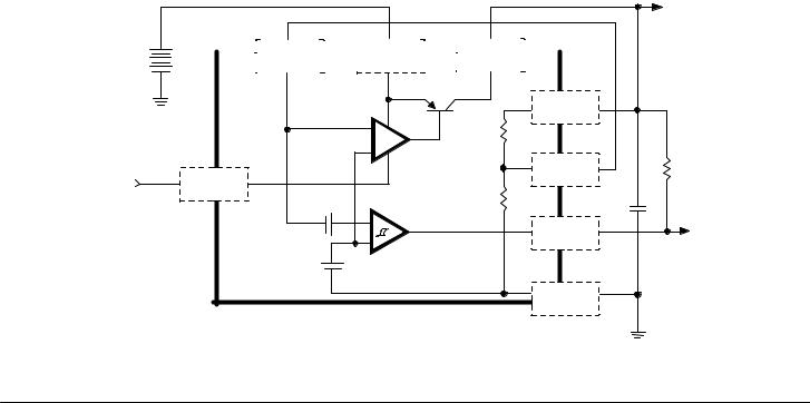
SPX2954 Block Diagram
Rev. 11/21/00
 Loading...