


Sipex Corporation SPX2975ACN-3.0, SPX2975ACN-3.3, SPX2975ACN-5.0, SPX2975ACP-3.0, SPX2975ACP-3.3 Datasheet
...
SPX2975
|
180 mA Low Dropout Voltage Regulators |
FEATURES |
APPLICATIONS |
• 3.0V, 3.3V and 5.0V Fixed Output Voltages |
• Battery Powered Systems |
• Very Low Quiescent Current |
• Cordless Telephones |
• Low Dropout Voltage |
• Radio Control Systems |
• Extremely Tight Load And Line Regulation |
• Portable/Palm Top/Notebook Computers |
• Very Low Temperature Coefficient |
• Portable Consumer Equipment |
• Needs Only 1 F For Stability |
• Portable Instrumentation |
• Current & Thermal Limiting |
• Avionics |
• Unregulated DC Input Can Withstand -20V Reverse Battery |
• Automotive Electronics |
And +60V Positive Transients |
• SMPS Post-Regulator |
• Similar Replacement For LP2950/LP2951 Sockets |
• Voltage Reference |
SPX2975 SO-8 versions only
•Error Flag Warns Of Output Dropout
•LogicControlled Electronic Shutdown
•Output Programmable from 1.24 to 29V
PRODUCT DESCRIPTION
The SPX2975 is a low power voltage regulator. This device is an excellent choice for use in battery-powered applications such as cordless telephones, radio control systems, and portable computers. The SPX2975 features very low quiescent current and very low dropout voltage (Typ. 50mV at light load and 380 mV at 180 mA). This includes a tight initial tolerance of 0.5% typ., extremely good load and line regulation 0.05% typ. and very low output temperature coefficient, making the SPX2975 useful as a low-power voltage reference. Other additional key features include higher output current (150mA), positive transient protection up to 60V (Load dump), and the ability to survive an unregulated input voltage transient of -20V below ground (reverse battery).
The error flag output feature is used as power-on reset for warning of a low output voltage, due to falling voltage input of batteries. Another feature is the logic-compatible shutdown input which enables the regulator to be switched on and off. The SPX2975 is offered in a 3-pin TO-92 package compatible with other 5V regulators. The SPX2975 is available in 8-pin plastic, SO-8 packages.
PIN CONNECTIONS
|
8-Pin Surface Mount (S) |
|
TO-92 (N) |
|||
VOUT |
1 |
8 |
VIN |
1 |
2 |
3 |
|
|
|
||||
SENSE |
2 |
7 |
FEEDBACK |
|
|
|
SHUTDOWN |
3SPX2975 6 |
5V TAP |
V |
|
VOUT |
|
|
|
|
|
|
||
|
|
|
|
IN |
GND |
|
GND |
4 |
5 |
ERROR |
|
|
|
|
|
|
||||
Top View |
Bottom View |
|
Rev. 10/30/00

SPX2975
ABSOLUTE MAXIMUM RATINGS
Power Dissipation.......................................... |
Internally Limited |
Lead Temp. (Soldering, 5 Seconds) ................................ |
260°C |
Storage Temperature Range ............................ |
-65° to +150°C |
Operating Junction Temperature Range (Note 10) |
|
SPX2975................................................... |
-55° to +150°C |
SPX2975AC/SPX2975C .......................... |
-40° to +125°C |
Input Supply Voltage (Survival) |
......................-20V to +60V |
Feedback Input Voltage .................................. |
-1.5V to +30V |
Shutdown Input Voltage.................................. |
-0.3V to +30V |
Error Comparator Output ................................ |
-0.3V to +30V |
ESD Rating ............................................................. |
2KV Min |
ELECTRICAL CHARACTERISTICS at VS=15V, TA=25°C, unless otherwise specified. Boldface apply over the full operating temperature range.
PARAMETER |
CONDITIONS |
|
SPX2975AC |
|
|
|
SPX2975C |
|
UNITS |
||
|
(Note 2) |
Min |
|
Typ |
Max |
|
Min |
Typ |
Max |
|
|
Output Voltage |
TJ = 25°C |
3.2835 |
|
3.3 |
|
3.3165 |
|
3.267 |
3.3 |
3.333 |
V |
|
-25°C ≤TJ ≤85°C |
3.267 |
|
|
|
3.333 |
|
3.2505 |
|
3.695 |
|
|
-40°C ≤TJ≤ +125°C |
3.2608 |
|
|
|
3.3396 |
|
3.2604 |
|
3.3396 |
|
Output Voltage |
100 A ≤IL ≤180 mA |
3.2505 |
|
3.3 |
|
3.3495 |
|
3.201 |
3.3 |
3.399 |
V |
|
TJ ≤TJMAX |
|
|
|
|
|
|
|
|
|
|
Output Voltage |
TJ = 25°C |
4.975 |
|
5.0 |
|
5.025 |
|
4.95 |
5.0 |
5.05 |
V |
|
-25°C ≤TJ ≤85°C |
4.95 |
|
5.0 |
|
5.050 |
|
4.925 |
5.0 |
5.075 |
|
|
-40°C ≤TJ≤ +125°C |
4.94 |
|
5.0 |
|
5.06 |
|
4.90 |
5.0 |
5.10 |
|
Output Voltage |
100 A ≤IL ≤180 mA |
4.925 |
|
5.0 |
|
5.075 |
|
4.85 |
5.0 |
5.15 |
V |
|
TJ ≤TJMAX |
|
|
|
|
|
|
|
|
|
|
Output Voltage |
|
|
|
20 |
|
|
|
|
50 |
|
ppm/°C |
Temperature Coefficient |
(Note 1) |
|
|
|
|
|
|
|
|
|
|
Line Regulation (Note 3) |
6V ≤VIN ≤30V (Note 4) |
|
|
0.03 |
|
0.1 |
|
|
0.04 |
0.2 |
% |
Load Regulation (Note 3) |
100 A ≤IL ≤ 180 mA |
|
|
0.04 |
|
0.1 |
|
|
0.1 |
0.2 |
% |
Dropout Voltage (Note 5) |
IL = 100 A |
|
|
50 |
|
80 |
|
|
50 |
80 |
mV |
|
IL = 100 mA |
|
|
380 |
|
450 |
|
|
380 |
450 |
|
|
IL = 180 mA |
|
|
450 |
|
500 |
|
|
450 |
500 |
|
Ground Current |
IL = 100 A |
|
|
150 |
|
170 |
|
|
150 |
170 |
A |
|
IL = 100 mA |
|
|
8 |
|
12 |
|
|
8 |
12 |
mA |
|
IL = 180 mA |
|
|
18 |
|
22 |
|
|
18 |
22 |
mA |
Current Limit |
VOUT = 0 |
|
|
130 |
|
200 |
|
|
130 |
200 |
mA |
|
|
|
|
|
|
|
|
|
|
|
|
Thermal Regulation |
|
|
|
0.05 |
|
0.2 |
|
|
0.05 |
0.2 |
%/W |
|
|
|
|
|
|
|
|
|
|
|
|
Output Noise, |
CL = 1 F |
|
|
430 |
|
|
|
|
430 |
|
V rms |
10Hz to 100kHz |
CL = 200 F |
|
|
160 |
|
|
|
|
160 |
|
|
|
CL = 13.3 F |
|
|
100 |
|
|
|
|
100 |
|
|
|
(Bypass = 0.01 F |
|
|
|
|
|
|
|
|
|
|
|
pins 7 to 1(SPX2975)) |
|
|
|
|
|
|
|
|
|
|
8-Pin Versions Only |
|
|
|
SPX2975AC |
|
|
|
|
SPX2975C |
|
|
Reference Voltage |
|
1.22 |
|
1.235 |
|
1.25 |
|
1.21 |
1.23 |
1.26 |
V |
|
|
|
|
|
|
|
|
|
|
|
|
Reference Voltage |
Over Temperature |
1.19 |
|
|
|
1.27 |
|
1.18 |
|
1.28 |
V |
|
( Note 6) |
|
|
|
|
|
|
|
|
|
|
Feedback Pin Bias Current |
|
|
|
40 |
|
60 |
|
|
40 |
60 |
nA |
|
|
|
|
|
|
|
|
|
|
|
|
Reference Voltage Temperature |
(Note 7) |
|
|
20 |
|
|
|
|
50 |
|
ppm/°C |
Coefficient |
|
|
|
|
|
|
|
|
|
|
|
Feedback Pin Bias Current |
|
|
|
0.1 |
|
|
|
|
0.1 |
|
nA/°C |
Temperature Coefficient |
|
|
|
|
|
|
|
|
|
|
|
Output Leakage Current |
VOH = 30V |
|
|
0.01 |
|
1 |
|
|
0.01 |
1 |
A |
Output Low Voltage |
VIN = 4.5V |
|
|
150 |
|
250 |
|
|
150 |
250 |
mV |
|
IOL = 400 A |
|
|
|
|
|
|
|
|
|
|
Upper Threshold Voltage |
(Note 8) |
40 |
|
60 |
|
|
|
40 |
60 |
|
mV |
|
|
|
|
|
|
|
|
|
|
|
|
Lower Threshold Voltage |
(Note 8) |
|
|
75 |
|
95 |
|
|
75 |
95 |
mV |
|
|
|
|
|
|
|
|
|
|
|
|
Hysteresis |
(Note 8) |
|
|
15 |
|
|
|
|
15 |
|
mV |
|
|
|
|
|
|
|
|
|
|
|
|
|
|
|
|
|
|
|
|
|
|
|
|
Rev. 10/30/00
|
|
|
|
|
|
|
|
|
|
|
|
SPX2975 |
|
|
|
|
|
|
|
|
|
|
|
|
|
|
|
|
PARAMETER |
CONDITIONS |
|
SPX2975AC |
|
|
SPX2975C |
|
|
UNITS |
|||
|
|
(Note 2) |
Min |
|
Typ |
Max |
Min |
Typ |
|
|
|
||
|
|
|
|
|
|
|
|
Max |
|
|
|
|
|
|
Input Logic Voltage |
Low (Regulator ON) |
|
|
1.3 |
|
0.7 |
|
1.3 |
|
0.7 |
|
V |
|
|
High (Regulator OFF) |
2 |
|
|
|
|
2 |
|
|
|
|
|
|
Shut Down Pin Input Current |
VS = 2.4V |
|
|
30 |
|
50 |
|
30 |
|
50 |
|
A |
|
|
VS = 30V |
|
|
675 |
|
800 |
|
675 |
|
800 |
|
|
|
Regulator Output Current in |
(Note 9) |
|
|
3 |
|
10 |
|
3 |
|
10 |
|
A |
|
Shutdown |
|
|
|
|
|
|
|
|
|
|
|
|
|
|
|
|
|
|
|
|
|
|
|
|
|
|
Note 1: Output or reference voltage temperature coefficients defined as the worst case voltage change divided by the total temperature range.
Note 2: Unless otherwise specified all limits guaranteed for TJ = 25°C, VIN = 6V, IL = 100 A and CL = 1 F. Additional conditions for the 8-pin versions are
feedback tied to 5V tap and output tied to output sense (VOUT = 5V) and VSHUTDOWN ≤ 0.8V.
Note 3: Regulation is measured at constant junction temperature, using pulse testing with a low duty cycle. Changes in output voltage due to heating effects are covered under the specification for thermal regulation.
Note 4: Line regulation for the SPX2975 is tested at 150°C for IL = 1mA. For IL = 100 A and TJ = 125°C, line regulation is guaranteed by design to 0.2%. See typical performance characteristics for line regulation versus temperature and load current.
Note 5: Dropout voltage is defined as the input to output differential at which the output voltage drops 100mV below its nominal value measured at 1V differential at very low values of programmed output voltage, the minimum input supply voltage of 2V ( 2.3V over temperature) must be taken into account.
Note 6: VREF ≤VOUT ≤ (VIN - 1V), 2.3 ≤VIN≤30V, 100 A≤IL≤ 100 mA, TJ ≤ TJMAX.
Note 7: Comparator thresholds are expressed in terms of a voltage differential at the feedback terminal below the nominal reference voltage measured at 6V input. To express these thresholds in terms of output voltage change, multiply by the error amplifier gain = VOUT/VREF = (R1 + R2)/R2. For example, at a programmed output voltage of 5V, the error output is guaranteed to go low when the output drops by 95mV x 5V/1.235 = 384mV. Thresholds remain constant as a percent of VOUT as VOUT is varied, with the dropout warning occurring at typically 5% below nominal, 7.5% guaranteed.
Note 8: VSHUTDOWN ≥ 2V, VIN ≤ 30V, VOUT =0, Feedback pin tied to 5V Tap. Note 9: All typical values are not guaranteed. The value could vary from lot to lot.
Note 10: The junction -to-ambient thermal resistance of the TO-92 package is 180°C/ W with 0.4” leads and 160°C/ W with 0.25” leads to a PC board.
The thermal resistance of the 8-Pin DIP package is 105°C/W junction-to-ambient when soldered directly to a PC board. Junction-to-ambient thermal resistance for the SOIC (S) package is 160°C/W.
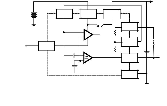
BLOCK DIAGRAM
|
UNREGULATED DC |
|
|
|
|
|
|
|
7 |
|
|
8 |
1 |
|
5V @ 180mA |
|
|
|
|
MAX |
|||
|
+ |
|
|
|
|
|
|
|
FEEDBACK |
|
INPUT |
OUTPUT |
|
|
|
|
|
|
|
|
|
2 |
|
|
|
|
|
|
|
SENSE |
|
|
|
|
+ |
|
180kΩ .. |
6 |
|
|
|
|
|
|
|
||
|
3 |
|
_ |
ERROR |
|
|
|
FROM |
|
|
|
|
|
||
|
|
AMPLIFIER |
|
|
330kΩ .. |
||
|
|
|
|
5V TAP |
|||
CMOS OR |
|
|
|
|
|
||
TTL |
SHUTDOWN |
|
|
|
|
|
+ |
|
|
|
|
|
60kΩ .. |
5 |
|
|
|
+ |
|
|
|
1µF.. |
|
|
|
+ |
|
|
______ |
||
|
60 mV |
|
|
|
|
||
|
|
_ |
ERROR DETECTION |
ERROR |
|
||
|
|
|
|
TO CMOS OR |
|||
|
|
+ 1.23V |
|
|
|||
|
|
|
COMPARATOR |
|
|
||
|
|
|
|
|
TTL |
||
|
|
|
|
|
|
4 |
|
|
|
|
|
|
|
|
|
|
|
REFERENCE |
|
|
GROUND |
|
|
|
|
|
|
|
|
|
|
SPX2975 Block Diagram
Rev. 10/30/00
 Loading...