


Sipex Corporation SPX2702AU5, SPX2702T3, SPX2702T5, SPX2702U3, SPX2702U5 Datasheet
...
|
SPX2700/01/02 |
|
700mA Low Dropout Voltage Regulators |
|
With Shutdown |
|
(PRELIMINARY INFORMATION) |
FEATURES |
APPLICATIONS |
• Output Current 700mA at 3.3V and 5V |
• Battery Powered Systems |
• Internal Short Circuit Current Limit |
• Cordless Telephones |
• Dropout Voltage 0.5V at 700mA Output |
• Automotive Electronics |
• Extremely Tight Load and Line Regulation |
• Portable/ Palm Top / Notebook Computers |
• Very Low Temperature Coefficient |
• Portable Consumer Equipment |
• Mirror Image Insertion Protection |
• Portable Instrumentation |
• Unregulated DC Input Can Withstand -20V Reverse Battery |
• SMPS Post-Regulator |
and +60V Positive Transients |
• Voltage Reference |
• Direct Replacement For LM2937 Socket |
|
PRODUCT DESCRIPTION
The SPX2700/01/02 are a low power positive voltage regulators. The SPX2700/01/02 offers 700mA output current with a dropout voltage of only 0.5V and over temperature dropout is up to 1V. The quiescent current is 10mA at differential output of 5V and output current of 700mA. A higher quiescent current can exist when the device is in dropout mode (VIN -VOUT≤ 3V).
The regulator will automatically shut down to protect both the internal circuits and the load. This device also features short circuit and thermal overload protection.
The SPX2700/01/02 is offered in 3 and 5 pin TO-220, TO-263 and 3-pin SOT-223 packages compatible with other 5V and 3.3V regulators, TO-263 and 3-pin SOT-223. The device is offered in standard output voltages of 5V and 3.3V as well as in adjustable output regulator.
TO-263-5 (T)
SPX |
2700/01/02 |
1 2 3 4 5
Top View
|
|
|
|
|
|
PIN CONNECTIONS |
|
|
|
|
|
|
|
|
||
TO-220-5 (U) |
|
|
|
TO-220-3 (U) |
TO-263-3 (T) |
SOT-223 (M3) |
||||||||||
|
SPX |
|
|
|
|
|
|
|
SPX2700 |
SPX2700 |
||||||
|
|
Five Lead Package Pin Functions: |
SPX2700 |
|
|
|
||||||||||
|
2701/02 |
|
1) |
Error |
Adjust |
1 |
2 |
3 |
1 |
2 |
3 |
|||||
|
|
|
|
|
||||||||||||
1 |
2 |
3 |
4 |
5 |
1 |
2 |
3 |
|
|
|
|
|
|
|||
2) |
Input |
Shutdown |
|
|
|
|
|
|
||||||||
|
|
|
|
|
|
|
|
|
|
|
VIN GND VOUT |
|||||
|
|
|
|
|
3) GND |
GND |
|
|
|
|
|
|
||||
|
|
|
|
|
4) |
Output |
Input |
|
|
|
VIN |
GND |
VOUT |
Top View |
||
|
|
|
|
|
5) |
Shutdown |
Output |
|
|
|
|
|
|
|||
|
|
|
|
|
|
|
|
Top View |
|
|
|
|||||
|
|
|
|
|
|
|
|
|
|
|
|
|
|
|||
Front View |
|
|
|
VIN GND VOUT |
|
|
|
|
|
|
||||||
|
|
|
|
|
|
|
|
Front View |
|
|
|
|
|
|
||
Rev. 10/25/00

SPX2700/01/02
ABSOLUTE MAXIMUM RATINGS
Power Dissipation.......................................... |
Internally Limited |
Lead Temp. (Soldering, 10 Seconds) .............................. |
260°C |
Feedback Input Voltage...................................... |
-1.5V to +30V |
Shutdown Input Voltage..................................... |
-0.3V to +30V |
Error Comparator Output ................................... |
-0.3V to +30V |
Input Supply Voltage |
Continuous ......................... |
+12V |
|
Transient................ |
-20V to +60V |
Storage Temperature Range ......................... |
-65° to +150°C |
|
Operating Junction Temperature Range ..... |
-40°C to +125°C |
|
ESD Rating |
..................................... |
2KV Min |
ELECTRICAL CHARACTERISTICS at VIN = VO + 5V, IO = 700mA, CO = 10 F, unless otherwise specified. Limits in Boldface type apply over the entire operating temperature range. All other specifications are TA = 25°C.
Parameter |
Conditions |
Typ. |
SPX2700/01/02A |
SPX2700/01/02 |
Units |
||
|
(Note 2) |
|
Min |
Max |
Min |
Max |
|
3.3V Version |
|
|
|
|
|
|
|
Output Voltage |
-40°C≤TJ≤+125°C |
3.3 |
3.267 |
3.333 |
3.234 |
3.366 |
V |
|
3.3 |
3.217 |
3.382 |
3.185 |
3.415 |
|
|
|
1mA≤ IL≤500mA |
|
|
|
|
|
|
5V Version |
|
|
|
|
|
|
|
Output Voltage |
-40°C≤TJ≤+125°C |
5.0 |
4.950 |
5.050 |
4.900 |
5.100 |
V |
|
5.0 |
4.880 |
5.120 |
4.870 |
5.130 |
|
|
|
1mA≤ IL≤700mA |
|
|
|
|
|
|
All Voltage Options |
|
|
|
|
|
|
|
Output Voltage |
|
20 |
|
100 |
|
150 |
ppm/°C |
Temperature Coefficient |
(Note1) |
|
|
|
|
|
|
Line Regulation (Note 3) |
6V≤ VIN≤30V (Note4) |
0.03 |
|
0.1 |
|
0.20 |
%max |
|
|
|
|
0.40 |
|
0.80 |
|
Load Regulation (Note 3) |
IL = 1 to 700 |
0.04 |
|
0.20 |
|
0.30 |
%max |
|
IL = 0.1 to 1mA |
|
|
0.30 |
|
0.50 |
|
Dropout Voltage (Note 5) |
IL = 1mA |
60 |
|
100 |
|
100 |
mV |
|
|
|
|
150 |
|
150 |
|
|
IL = 700mA |
375 |
|
400 |
|
400 |
|
|
|
|
|
500 |
|
500 |
|
Ground Current |
IL = 1mA |
100 |
|
150 |
|
150 |
µA |
|
|
|
|
180 |
|
180 |
mA |
|
|
4.5 |
|
2 |
|
2 |
|
|
|
15 |
|
2.5 |
|
2.5 |
|
|
|
|
|
14 |
|
14 |
|
|
IL = 700mA |
20 |
|
16 |
|
16 |
|
|
|
|
20 |
|
20 |
|
|
|
|
|
|
22 |
|
22 |
|
Current Limit |
VOUT = 0 |
|
|
700 |
|
700 |
mA |
|
|
|
|
800 |
|
800 |
|
Thermal Regulation |
|
0.05 |
|
0.2 |
|
0.2 |
%/w |
|
|
|
|
|
|
|
|
Output Noise, 10Hz to 100kHz |
CL = 2.2µF |
400 |
1.0 |
0.60 |
1.0 |
0.60 |
µV |
IL = 100mA |
CL = 33µF |
200 |
|
|
|
|
Vrms |
Adjustable Versions Only |
|
|
|
|
|
|
|
Reference Voltage |
Over Temperature |
1.235 |
1.210 |
1.260 |
1.200 |
1.270 |
V |
|
(Note 6) |
|
1.200 |
1.270 |
1.980 |
1.272 |
|
|
|
|
1.185 |
1.285 |
1.185 |
1.285 |
|
Feedback Pin Bias Current |
|
20 |
|
40 |
|
60 |
nA |
|
|
|
|
60 |
|
80 |
|
Reference Voltage Temperature |
(Note 7) |
50 |
|
|
|
|
ppm/°C |
Coefficient |
|
|
|
|
|
|
|
|
|
|
|
|
|
|
|
Feedback Pin Bias Current |
|
0.1 |
|
|
|
|
NA/°C |
Temperature Coefficient |
|
|
|
|
|
|
|
|
|
|
|
|
|
|
|
Rev. 10/25/00
SPX2700/01/02
ELECTRICAL CHARACTERISTICS at VIN = VO + 5V, IO = 700mA, CO = 22 F, unless otherwise specified. Limits in Boldface type apply over the entire operating temperature range. All other specifications are TA = 25°C.
Parameter |
Conditions |
Typ. |
SPX2700/01/02A |
SPX2700/01/02 |
Units |
|||
|
|
|
Min |
Max |
Min |
Max |
|
|
Error Comparator |
|
|
|
|
|
|
|
|
Output Leakage Current |
VOH = 30V |
0.01 |
|
1.00 |
|
1.00 |
|
µA |
|
|
|
|
2.00 |
|
2.00 |
|
|
Output Low Voltage |
VIN = 4.5V |
150 |
|
250 |
|
250 |
|
mV |
|
IOL = 400µA |
|
|
400 |
|
400 |
|
|
Upper Threshold Voltage |
(Note 8) |
60 |
40 |
|
40 |
|
|
mV |
|
|
|
25 |
|
25 |
|
|
|
Lower Threshold Voltage |
(Note 8) |
75 |
|
95 |
|
95 |
|
mV |
|
|
|
|
140 |
|
140 |
|
|
Hysteresis |
(Note 8) |
15 |
|
|
|
|
|
mV |
|
|
|
|
|
|
|
|
|
Shutdown Input |
|
|
|
|
|
|
|
|
Input Logic Voltage |
Low (Regulator ON) |
|
2.0 |
0.7 |
2.0 |
0.7 |
|
V |
|
High (Regulator OFF) |
|
|
|
|
|
||
Shutdown Pin Input Current |
VS = 2.4V |
30 |
|
50 |
|
90 |
|
µA |
|
|
|
|
100 |
|
150 |
|
|
|
|
|
|
600 |
|
800 |
|
|
|
VS = 30V |
450 |
|
750 |
|
1000 |
|
|
Regulator Output Current In |
|
3 |
10 |
|
|
15 |
|
µA |
Shutdown |
|
|
20 |
|
|
25 |
|
|
|
|
|
|
|
|
|
|
|
Note 1: Output or reference voltage temperature coefficients defined as the worst case voltage change divided by the total temperature range.
Note 2: Unless otherwise specified all limits are guaranteed for Tj = 25°C, VIN = 6V, IL = 100 A and CL = 1 F. Additional conditions for the 8-pin versions are
feedback tied to 5V tap and output tied to output sense (VOUT = 5V) and VSHUTDOWN ≤ 0.8V.
Note 3: Regulation is measured at constant junction temperature, using pulse testing with a low duty cycle. Changes in output voltage due to heating effects are covered under the specification for thermal regulation.
Note 4: Line regulation for the SPX2700/01/02 is tested at 150°C for IL = 1 mA. For IL = 100 A and TJ = 125°C, line regulation is guaranteed by design to 0.2%. See typical performance characteristics for line regulation versus temperature and load current.
Note 5: Dropout voltage is defined as the input to output differential at which the output voltage drops 100 mV below its nominal value measured at 1V differential at very low values of programmed output voltage, the minimum input supply voltage of 2V ( 2.3V over temperature) must be taken into account.
Note 6: VREF ≤VOUT ≤ (Vin - 1V), 2.3 ≤Vin≤30V, 100 A≤IL≤ 250 mA, TJ ≤ TJMAX.
Note 7: Comparator thresholds are expressed in terms of a voltage differential at the feedback terminal below the nominal reference voltage measured at 6V input. To express these thresholds in terms of output voltage change, multiply by the error amplifier gain = VOUT/VREF = (R1 + R2)/R2. For example, at a programmed output voltage of 5V, the Error output is guaranteed to go low when the output drops by 95 mV x 5V/1.235 = 384 mV. Thresholds remain constant as a percent of VOUT as VOUT is varied, with the dropout warning occurring at typically 5% below nominal, 7.5% guaranteed.
Note 8: VSHUTDOWN ≥ 2V, VIN ≤ 30V, VOUT =0, Feedback pin tied to 5V Tap.
Note 9: The junction -to-ambient thermal resistance of the TO-92 package is 180°C/ W with 0.4” leads and 160°C/ W with 0.25” leads to a PC board.
The thermal resistance of the 8-Pin DIP package is 105°C/W junction-to-ambient when soldered directly to a PC board. Junction-to-ambient thermal resistance for the SOIC (S) package is 160°C/W.
UNREGULATED DC
|
|
|
|
|
|
5V @ 700mA |
|
+ |
|
|
|
|
MAX |
|
|
|
|
|
|
|
|
FEEDBACK |
|
INPUT |
OUTPUT |
|
|
|
|
|
|
|
SENSE |
|
|
|
|
+ |
|
180kΩ .. |
|
|
|
|
|
|
|
|
|
|
|
_ |
ERROR |
|
|
FROM |
|
|
|
|
|
|
|
|
|
AMPLIFIER |
5V TAP |
330kΩ .. |
|
CMOS OR |
SHUTDOWN |
|
|
|
||
TTL |
|
|
|
|
+ |
|
|
|
|
|
|
60kΩ .. |
|
|
|
+ |
+ |
|
______ |
1µF.. |
|
60 mV |
|
|
|
||
|
|
_ |
|
ERROR |
|
|
|
|
|
ERROR DETECTION |
TO CMOS OR |
||
|
|
+ 1.23V |
|
COMPARATOR |
||
|
|
|
TTL |
|||
|
|
|
|
|
|
|
|
|
REFERENCE |
|
GROUND |
|
|
|
|
|
|
|
|
|
|
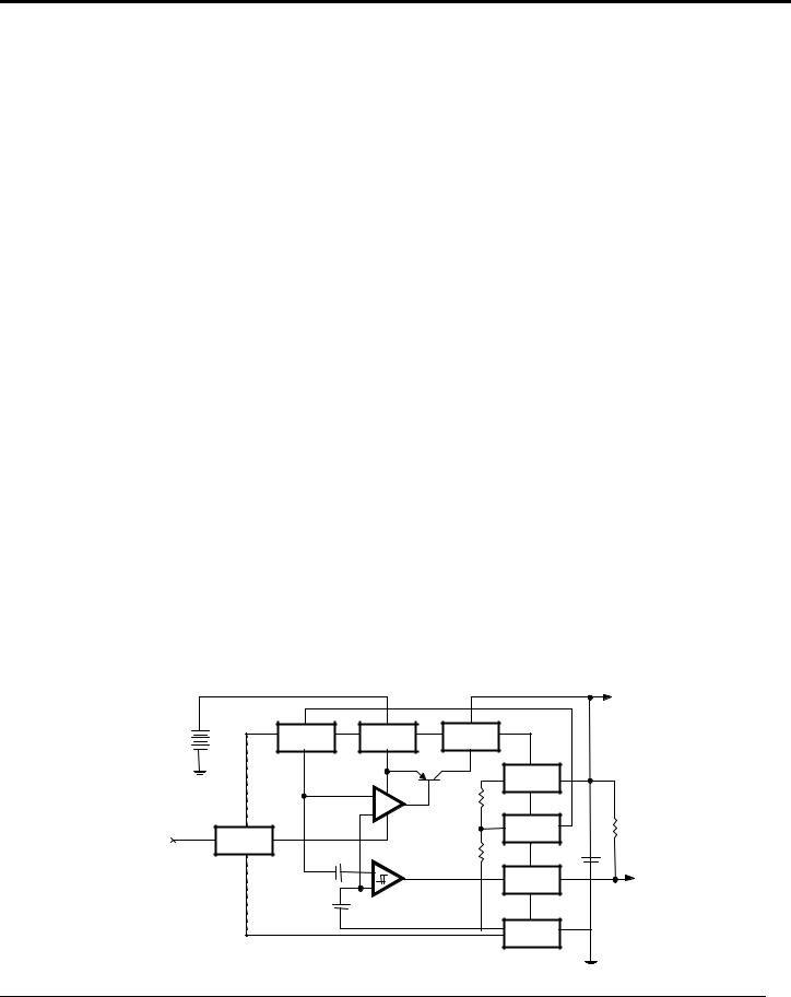
SPX2700/01/02 Block Diagram |
|
||||
Rev. 10/25/00
SPX2700/01/02
APPLICATION HINTS EXTERNAL CAPACITORS
The stability of the SPX2700/01/02 requires a 10µF or greater capacitor between output and ground. Oscillation could occur without this capacitor. Most types of tantalum or aluminum electrolytic works fine here. For operations below -25°C solid tantalum is recommended since the many aluminum types have electrolytes that freeze at about -30°C. The ESR of about 5Ω or less and resonant frequency above 500 kHz are the most important parameters in the value of the capacitor. The capacitor value may be increased without limit.
At lower values of output current, less output capacitance is required for stability. For the currents below 10mA the value of the capacitor can be reduced to 22µF and 0.15µF for 1mA. More output capacitance is needed for the 8-pin version at voltages below 5V since it runs the error amplifier at lower gain. At worst case 22µF or greater must be used for the condition of 750mA load at 1.23V output.
The SPX2700/01/02, unlike other low dropout regulators will remain stable and in regulation with no load in addition to the internal voltage divider. This feature is especially important in applications like CMOS RAM keep-alive. When setting the output voltage of the SPX2700/01/02 version with external resistors, a minimum load of 5mA is recommended. If there is more than 10 inches of wire between the input and the AC filter capacitor or if a battery is used as the input then a 1µA tantalum or aluminum electrolytic capacitor should be placed from the input to the ground.
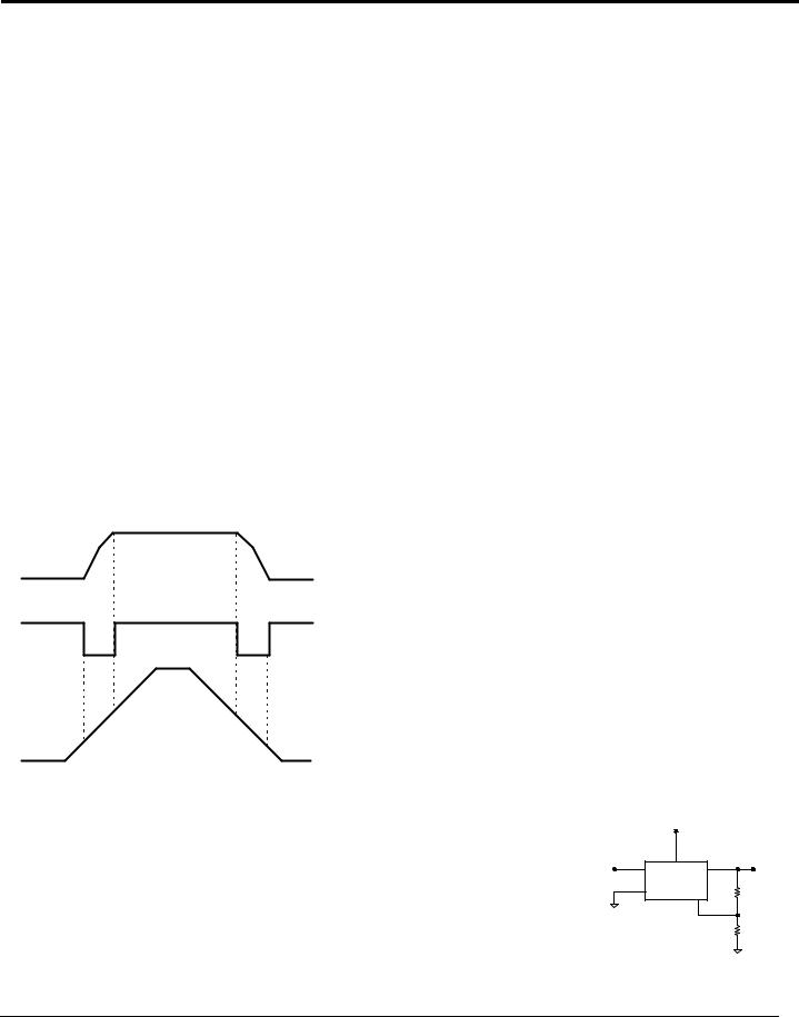
ERROR DETECTION COMPARATOR OUTPUT
4.75V
OUTPUT
VOLTAGE
_______
ERROR*
+5.0V |
+ |
VOLTAGEINPUT +1.3V |
+ |
* See Application Info. _______
Figure 1. ERROR Output Timing
The Comparator produces a logic low output whenever the SPX2700/01/02 output falls out of regulation by more than around 5%. This is around 75mV offset divided by the 1.235 reference voltage. This trip level remains 5% below normal regardless of the programmed output voltage of the regulator. Figure 1 shows the timing diagram depicting the ERROR signal and the regulator output voltage as the SPX2700/01/02 input is ramped up and down. The ERROR signal becomes low at around 1.3V input, and goes
high around 5V input (input voltage at which Vout = 4.75 ). Since the SPX2700/01/02’s dropout voltage is load dependent, the input voltage trip point (around 5V) will vary with the load current. The output voltage trip point (approx. 4.75V) does not vary with load. The error comparator has an open-collector output, which requires an external pull-up resistor. Depending on the system requirements the resistor may be returned to 5V output or other supply voltage. In determining the value of this resistor, note that the output is rated to sink 250µA, this value adds to battery drain in a low battery condition. Suggested values range from 100K to 1MΩ. If the output is unused this resistor is not required.
PROGRAMMING THE OUTPUT VOLTAGE OF SPX2700/01/02
The SPX2700/01/02 may be programmed for any output voltage between its 1.235V reference and its 30V maximum rating . As seen in Figure 2, an external pair of resistors is required. Refer to the below equation for the programming of the output voltage:
VOUT = VREF × (1 + R1\ R2)+ IFBR1
The VREF is 1.235 and IFB is the feedback bias current, nominally -20 nA. The minimum recommended load current of 1µA forces an upper limit of 1.2 MΩ on value of R2. If no load is presented the IFB produces an error of typically 2% in VOUT, which may be eliminated at room temperature by trimming R1. To improve the accuracy choose the value of R2 = 100k this reduces the error by 0.17% and increases the resistor program current by 12µA. Since the SPX2700/01/02 typically draws 100µA at no load with SHUTDOWN open-circuited this is a small price to pay
REDUCING OUTPUT NOISE
It may be an advantage to reduce the AC noise present at the output. One way is to reduce the regulator bandwidth by increasing the size of the output capacitor. This is the only way that noise can be reduced on the 3 lead SPX2700/01/02 but is relatively inefficient, as increasing the capacitor from 1µF to 220µF only decreases the noise
from 430µV to 160µVRMS for a 100 kHz bandwidth at 5V output. Noise could also be reduced fourfold by a bypass capacitor across R1,
since it reduces the high frequency gain from 4 to unity. Pick
CBYPASS 1 / 2πR1 × 200 Hz
or choose 0.01µF. When doing this, the output capacitor must be increased to 3.3µF to maintain stability. These changes reduce the
output noise from 430µV to 100µVRMS for a 100 kHz bandwidth at 5V output. With the bypass capacitor added, noise no longer scales
with output voltage so that improvements are more dramatic at higher
output voltages. |
SHUTDOWN |
|
VOUT |
|
VIN |
|
SPX2703 |
|
GND |
|
ADJ |
|
Fig.2 Adjustable Voltage Regulator |
Rev. 10/25/00
 Loading...