


Sipex Corporation SP705CN, SP705CP, SP705CU, SP705EN, SP705EP Datasheet
...®
SP705-708/813L/813M
Low Power Microprocessor Supervisory Circuits
■Precision Voltage Monitor: SP705/707/813L at 4.65V SP706/708/813M at 4.40V
■RESET Pulse Width - 200ms
■Independent Watchdog Timer - 1.6s Timeout (SP705/706/813L/813M)
■60μA Maximum Supply Current
■Debounced TTL/CMOS Manual Reset Input
■RESET Asserted Down to VCC = 1V
■Voltage Monitor for Power Failure or Low Battery Warning
■Available in 8-pin PDIP, NSOIC, and μSOIC packages
■Pin Compatible Enhancement to Industry Standard 705-708/813L Series
■Functionally Compatible to Industry Standard 1232 Series
DESCRIPTION…
The SP705-708/813L/813M series is a family of microprocessor (μP) supervisory circuits that integrate myriad components involved in discrete solutions which monitor power-supply and battery in μP and digital systems. The SP705-708/813L/813M series will significantly improve system reliability and operational efficiency when compared to solutions obtained with discrete components. The features of the SP705-708/813L/813M series include a watchdog timer, a μP reset, a Power Fail Comparator, and a manual-reset input. The SP705-708/813L/813M series is ideal for applications in automotive systems, computers, controllers, and intelligent instruments. The SP705-708/813L/813M series is an ideal solution for systems in which critical monitoring of the power supply to the μP and related digital components is demanded.
Part |
RESET |
RESET |
Manual |
|
|
PFI |
Number |
Threshold |
Active |
RESET |
Watchdog |
Accuracy |
|
|
|
|
|
|
|
|
SP705 |
4.65 V |
LOW |
YES |
YES |
|
4% |
|
|
|
|
|
|
|
SP706 |
4.40 V |
LOW |
YES |
YES |
|
4% |
|
|
|
|
|
|
|
SP707 |
4.65 V |
LOW and HIGH |
YES |
NO |
|
4% |
|
|
|
|
|
|
|
SP708 |
4.40 V |
LOW and HIGH |
YES |
NO |
|
4% |
|
|
|
|
|
|
|
SP813L |
4.65 V |
HIGH |
YES |
YES |
|
4% |
|
|
|
|
|
|
|
SP813M |
4.40V |
HIGH |
YES |
YES |
|
4% |
|
|
|
|
|
|
|
|
|
|
|
|
|
|
SP705DS/09 |
|
SP705 Low Power Microprocessor Supervisory Circuits |
© Copyright 2000 Sipex Corporation |
|||
1

ABSOLUTE MAXIMUM RATINGS
This is a stress rating only and functional operation of the device at these or any other conditions above those indicated in the operation sections of this specification is not implied. Exposure to absolute maximum rating conditions for extended periods of time may affect reliability and cause permanent damage to the device.
Vcc ....................................................................................... |
-0.3V to +6.0V |
All Other Inputs (Note 1) ......... |
-0.3V to (Vcc+0.3V) |
Input Current: |
|
Vcc ............................................................................................................. |
20mA |
GND ............................................................ |
20mA |
Output Current (all outputs) ......................... |
20mA |
ESD Rating ..................................................... |
4KV |
Continuous Power Dissipation
Plastic DIP (derate 9.09mW/°C above +70°C)727mW
SO (derate 5.88mW/°C above +70°C) ...... |
471mW |
Mini SO (derate 4.10mW/°C above +70°C) 330mW
Storage Temperature Range ....... |
-65°C to +160°C |
|
Lead Temperature (soldering, 10s) ............ |
+300°C |
|
SPECIFICATIONS
VCC = 4.75V to 5.50V for SP705/707/813L, VCC = 4.50V to 5.50V for SP706/708/813M, TA = TMIN to TMAX, unless otherwise noted, typical at 25oC.
PARAMETER |
MIN. |
TYP. |
MAX. |
UNITS |
|
CONDITIONS |
|
|
|
|
|
|
|
|
|
Operating Voltage Range, VCC |
1.0 |
|
5.5 |
V |
|
|
|
|
|
|
|
|
|
|
|
Supply Current, ISUPPLY |
|
40 |
60 |
μA |
|
|
|
|
|
MR=VCC or Floating, WDI Floating |
|||||
|
|
|
|
|
|
|
|
Reset Threshold |
4.50 |
4.65 |
4.75 |
V |
|
SP705, SP707, SP813L, Note 2 |
|
|
4.25 |
4.40 |
4.50 |
|
|
SP706, SP708, SP813M, Note 2 |
|
|
|
|
|
|
|
|
|
Reset Threshold Hysteresis |
|
40 |
|
mV |
|
Note 2 |
|
|
|
|
|
|
|
|
|
Reset Pulse Width, tRS |
140 |
200 |
280 |
ms |
|
Note 2 |
|
|
|
|
|
|
|
Note 2 |
|
RESET Output Voltage |
VCC-1.5 |
|
|
|
|
ISOURCE = 800μA |
|
|
0.8 |
|
0.40 |
V |
|
ISOURCE=4μA, VCC=1.1V |
|
|
|
|
|
|
ISINK = 3.2mA |
||
|
|
|
0.30 |
|
|
VCC = 1V, ISINK = 50μA |
|
Watchdog Timeout Period, tWD |
1.00 |
1.60 |
2.25 |
s |
|
SP705, SP706, SP813L, SP813M |
|
WDI Pulse Width, tWP |
50 |
|
|
ns |
|
VIL = 0.4V, VIH = 0.8XVCC |
|
WDI Input Threshold, |
|
|
|
|
|
SP705, SP706, SP813L, SP813M |
|
LOW |
3.5 |
|
0.8 |
V |
|
VCC = 5V |
|
HIGH |
|
|
|
|
|
|
|
|
|
|
|
|
|
|
|
WDI Input Current |
|
30 |
75 |
μA |
|
SP705, SP706, SP813L, SP813M |
|
|
-75 |
-20 |
|
|
|
WDI = VCC |
|
|
|
|
|
SP705, SP706, SP813L, SP813M |
|||
|
|
|
|
|
|
WDI = 0V |
|
|
|
|
|
|
|
|
|
SP705DS/09 |
SP705 Low Power Microprocessor Supervisory Circuits |
© Copyright 2000 Sipex Corporation |
2
SPECIFICATIONS
VCC = 4.75V to 5.50V for SP705/707/813L,813M, VCC = 4.50V to 5.50V for SP706/708, TA = TMIN to TMAX, unless otherwise noted, typical at 25oC.
|
PARAMETER |
MIN. |
TYP. |
MAX. |
UNITS |
|
CONDITIONS |
|||||||||
|
|
|
|
|
|
|
|
|
|
|
|
|
|
|
|
|
|
|
|
|
|
|
|
|
|
|
|
|
|
|
|
ISOURCE=800μA |
|
|
WDO Output Voltage |
VCC-1.5 |
|
|
|
|
V |
|||||||||
|
|
|
|
|
|
|
|
|
|
|
|
0.40 |
|
ISINK=3.2mA |
||
|
|
|
|
|
|
|
|
|
|
|
|
|
|
|||
|
|
|
|
|
|
|
|
|
|
|
|
|
|
|
|
|
|
|
|
Pull-Up Current |
100 |
250 |
|
600 |
μA |
|
|
= 0V |
|||||
|
MR |
|
|
|
|
MR |
||||||||||
|
|
|
|
|
|
|
|
|
|
|
|
|
|
|
|
|
|
|
|
|
|
|
|
|
|
|
|
|
|
|
|||
|
MR Pulse Width, tMR |
150 |
|
|
|
|
ns |
|
|
|
||||||
|
|
|
|
|
|
|
|
|
|
|
|
|
|
|
|
|
|
|
|
|
|
|
|
|
|
|
|
|
|
||||
|
MR Input Threshold |
|
|
|
|
|
|
|
|
|
||||||
|
LOW |
|
|
|
|
0.8 |
V |
|
|
|
||||||
|
HIGH |
2.0 |
|
|
|
|
|
|
|
|
||||||
|
|
|
|
|
|
|
|
|
|
|
|
|
|
|
|
|
|
|
|
|
|
|
|
|
|
|
|
|
|
|
|
|
|
|
MR to Reset Out Delay, tMD |
|
|
|
|
250 |
ns |
|
Note 2 |
|||||||
|
|
|
|
|
|
|
|
|
|
|
|
|
|
|
|
|
|
PFI Input Threshold |
1.20 |
1.25 |
|
1.30 |
V |
|
VCC = 5V |
||||||||
|
|
|
|
|
|
|
|
|
|
|
|
|
|
|
|
|
|
PFI Input Current |
-25.00 |
0.01 |
|
25.00 |
nA |
|
|
|
|||||||
|
|
|
|
|
|
|
|
|
|
|
|
|
|
|
|
|
|
|
|
|
|
|
|
|
|
|
ISOURCE = 800μA |
||||||
|
PFO Output Voltage |
VCC-1.5 |
|
|
|
|
V |
|||||||||
|
|
|
|
|
|
|
|
|
|
|
|
0.4 |
|
|
ISINK = 3.2mA |
|
|
|
|
|
|
|
|
|
|
|
|
|
|
|
|
|
|
|
|
|
|
|
|
|
|
|
|
|
|
|
|
|
|
|
Note 1: The input voltage limits on PFI and MR can be exceeded if the input current is less than 10mA.
Note 2: Applies to both RESET in the SP705-SP708 and RESET in the SP707/708/813L/813M.
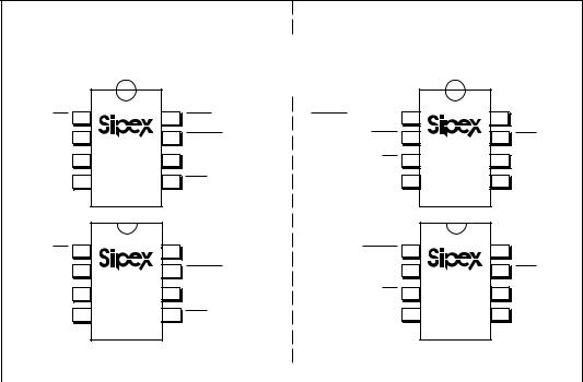
DIP and SOIC |
|
μSOIC |
||||
|
||||||
|
|
|
|
|
|
|
|
|
|
|
|
|
|
|
|
|
|
|
|
|
|
|
|
|
|
|
|
MR 1 |
|
8 |
WDO |
|
VCC |
2 |
SP705 |
7 |
RESET / RESET* |
|
3 |
6 |
|
|
GND |
SP706 |
WDI |
||
PFI |
4 |
SP813L |
5 |
PFO |
SP813M |
||||
MR 1 |
|
8 |
RESET |
|
VCC |
2 |
SP707 |
7 |
RESET |
|
3 |
6 |
|
|
GND |
SP708 |
N.C. |
||
PFI |
4 |
|
5 |
PFO |
RESET / RESET* |
1 |
|
8 |
WDI |
WDO |
2 |
SP705 |
7 |
PFO |
|
3 |
6 |
|
|
MR |
SP706 |
PFI |
||
VCC |
4 |
SP813L |
5 |
GND |
SP813M |
||||
RESET |
1 |
|
8 |
N.C. |
RESET |
2 |
SP707 |
7 |
PFO |
|
3 |
6 |
|
|
MR |
SP708 |
PFI |
||
VCC |
4 |
|
5 |
GND |
|
* SP813L/M only |
|
|
* SP813L/M only |
|
|
|||
|
|
|
|
|
Figure 1. |
Pinouts |
|
||
|
|
|
|
|
SP705DS/09 |
SP705 Low Power Microprocessor Supervisory Circuits |
© Copyright 2000 Sipex Corporation |
||
3

|
|
|
|
|
|
|
|
|
|
|
|
|
|
|
|
|
|
|
|
|
|
|
|
|
|
|
|
|
|
PIN DESCRIPTION |
|
|
|
||
|
|
|
|
|
|
|
|
|
|
|
|
|
|
|
|
|
|
|
|
|
|
|
|
|
|
|
|
|
|
|
|
|
|
|
|
|
NAME |
|
FUNCTION |
SP705/706 |
SP707/708 |
SP813L/813M |
|||||||||||||||||||||||||||||
|
|
|
|
|
|
|
|
|
|
|
|
|
|
|
|
|
|
|
|
|
|
|
|
|
|
|
|
|
|
|
|
|
|
|
|
|
|
|
|
|
|
|
|
|
|
|
|
|
|
|
|
|
|
|
|
|
|
|
|
|
|
|
|
|
|
DIP/ |
µ SOIC |
DIP/ |
µ SOIC |
DIP/ |
µ SOIC |
|
|
|
|
|
|
|
|
|
|
|
|
|
|
|
|
|
|
|
|
|
|
|
|
|
|
|
|
|
|
SOIC |
SOIC |
SOIC |
|||
|
|
|
|
|
|
|
|
|
|
|
|
|
|
|
|
|
|
|
|
|
|
|
|
|
|
|
|
|
|
|
|
|
|||
|
|
|
|
|
|
|
|
|
|
|
|
|
|
|
|
|
|
|
|
|
|
|
|
|
|
|
|
|
|
|
|
|
|
|
|
|
|
|
|
|
|
|
|
|
Manual Reset - This input triggers a reset pulse |
|
|
|
|
|
|
||||||||||||||||||||
|
|
|
|
|
|
|
|
|
when pulled below 0.8V. This active-LOW input |
|
|
|
|
|
|
||||||||||||||||||||
|
|
|
|
MR |
|
has an internal 250μA pull-up current. It can be |
1 |
3 |
1 |
3 |
1 |
3 |
|||||||||||||||||||||||
|
|
|
|
|
|
|
|
|
driven from a TTL or CMOS logic line or shorted |
|
|
|
|
|
|
||||||||||||||||||||
|
|
|
|
|
|
|
|
|
to ground with a switch |
|
|
|
|
|
|
||||||||||||||||||||
|
|
|
|
|
|
|
|
|
|
|
|
|
|
|
|
|
|
|
|
|
|
|
|
|
|
|
|
|
|
|
|
|
|
|
|
|
|
|
|
VCC |
|
+5V power supply |
2 |
4 |
2 |
4 |
2 |
4 |
|||||||||||||||||||||||
|
|
GND |
|
Ground reference for all signals |
3 |
5 |
3 |
5 |
3 |
5 |
|||||||||||||||||||||||||
|
|
|
|
|
|
|
|
|
|
|
|
|
|
|
|
|
|
|
|
|
|
|
|
|
|
|
|
|
|
|
|
|
|
|
|
|
|
|
|
|
|
|
|
|
Power-Fail Input - When this voltage monitor input |
|
|
|
|
|
|
||||||||||||||||||||
|
|
|
|
PFI |
|
is less than 1.25V, |
PFO |
goes LOW. Connect PFI |
4 |
6 |
4 |
6 |
4 |
6 |
|||||||||||||||||||||
|
|
|
|
|
|
|
|
|
to ground or VCC when not in use. |
|
|
|
|
|
|
||||||||||||||||||||
|
|
|
|
|
|
|
|
|
|
|
|
|
|
|
|
|
|
|
|
|
|
|
|
|
|
|
|
|
|
|
|
|
|
|
|
|
|
|
|
|
|
|
|
|
Power-Fail Output - This output is HIGH until PFI |
|
|
|
|
|
|
||||||||||||||||||||
|
|
|
PFO |
|
5 |
7 |
5 |
7 |
5 |
7 |
|||||||||||||||||||||||||
|
|
|
|
is less than 1.25V. |
|||||||||||||||||||||||||||||||
|
|
|
|
|
|
|
|
|
|
|
|
|
|
|
|||||||||||||||||||||
|
|
|
|
|
|
|
|
|
|
|
|
|
|
|
|
|
|
|
|
|
|
|
|
|
|
|
|
|
|
|
|
|
|
|
|
|
|
|
|
|
|
|
|
|
Watchdog Input - If this input remains HIGH or |
|
|
|
|
|
|
||||||||||||||||||||
|
|
|
|
|
|
|
|
|
LOW for 1.6s, the internal watchdog timer times |
|
|
|
|
|
|
||||||||||||||||||||
|
|
|
|
|
|
|
|
|
out and |
WDO |
goes LOW. Floating WDI or |
|
|
|
|
|
|
||||||||||||||||||
|
|
|
WDI |
|
connecting WDI to a high-impedance tri-state |
6 |
8 |
- |
- |
6 |
8 |
||||||||||||||||||||||||
|
|
|
|
buffer disables the watchdog feature. The internal |
|||||||||||||||||||||||||||||||
|
|
|
|
|
|
|
|
|
|
|
|
|
|
|
|||||||||||||||||||||
|
|
|
|
|
|
|
|
|
watchdog timer clears whenever |
RESET |
|
is |
|
|
|
|
|
|
|||||||||||||||||
|
|
|
|
|
|
|
|
|
asserted, WDI is tri-stated, or whenever WDI sees |
|
|
|
|
|
|
||||||||||||||||||||
|
|
|
|
|
|
|
|
|
a rising or falling edge. |
|
|
|
|
|
|
||||||||||||||||||||
|
|
|
|
|
|
|
|
|
|
|
|
|
|
|
|
|
|
|
|
|
|
|
|
|
|
|
|
|
|
|
|
|
|
|
|
|
|
|
N.C. |
|
No Connect. |
- |
- |
6 |
8 |
- |
- |
||||||||||||||||||||||||
|
|
|
|
|
|
|
|
|
|
|
|
|
|
|
|
|
|
|
|
|
|
|
|
|
|
|
|
|
|
|
|
|
|
|
|
|
|
|
|
|
|
|
|
|
|
|
|
|
|
|
|
|
|
||||||||||||||||||
|
|
|
|
|
|
|
|
|
Active-LOW RESET Output - This output pulses |
|
|
|
|
|
|
||||||||||||||||||||
|
|
|
|
|
|
|
|
|
LOW for 200ms when triggered and stays LOW |
|
|
|
|
|
|
||||||||||||||||||||
|
|
|
|
|
|
|
|
|
whenever VCC is below the reset threshold (4.65V |
|
|
|
|
|
|
||||||||||||||||||||
|
|
|
|
|
|
|
|
|
for the SP705/707/813L and 4.40V for the |
7 |
1 |
7 |
1 |
- |
- |
||||||||||||||||||||
|
RESET |
||||||||||||||||||||||||||||||||||
|
|
SP706/708). It remains LOW for |
200ms after Vcc |
||||||||||||||||||||||||||||||||
|
|
|
|
|
|
|
|
|
|
|
|
|
|
|
|||||||||||||||||||||
|
|
|
|
|
|
|
|
|
|
|
|
|
|
|
|
|
|||||||||||||||||||
|
|
|
|
|
|
|
|
|
rises above the reset threshold or MR goes from |
|
|
|
|
|
|
||||||||||||||||||||
|
|
|
|
|
|
|
|
|
LOW to HIGH. A watchdog timeout will not trigger |
|
|
|
|
|
|
||||||||||||||||||||
|
|
|
|
|
|
|
|
|
RESET unless |
|
WDO |
is connected to |
MR. |
|
|
|
|
|
|
|
|||||||||||||||
|
|
|
|
|
|
|
|
|
|
|
|
|
|
|
|
|
|
|
|
|
|
|
|
|
|
|
|
|
|
|
|
|
|
|
|
|
|
|
|
|
|
|
|
|
Watchdog Output - This output pulls LOW when |
|
|
|
|
|
|
||||||||||||||||||||
|
|
|
|
|
|
|
|
|
the internal watchdog timer finishes its 1.6s count |
|
|
|
|
|
|
||||||||||||||||||||
|
|
|
|
|
|
|
|
|
and does not go HIGH again until the watchdog is |
|
|
|
|
|
|
||||||||||||||||||||
|
|
|
|
|
|
|
|
|
|
|
|
|
|
|
|
|
|
|
|
|
|
|
|
|
|
||||||||||
|
|
|
|
|
|
|
|
|
cleared. WDO also goes LOW during low-line |
|
|
|
|
|
|
||||||||||||||||||||
|
|
WDO |
|
conditions. |
Whenever VCC is below the reset |
8 |
2 |
- |
- |
8 |
2 |
||||||||||||||||||||||||
|
|
|
|
|
|
|
|
|
threshold, WDO stays LOW. However, unlike |
|
|
|
|
|
|
||||||||||||||||||||
|
|
|
|
|
|
|
|
|
|
|
|
|
|
|
|
|
|
|
|
|
|
|
|
|
|
||||||||||
|
|
|
|
|
|
|
|
|
RESET, WDO does not have a minimum pulse |
|
|
|
|
|
|
||||||||||||||||||||
|
|
|
|
|
|
|
|
|
width. As |
soon |
as VCC is above the reset |
|
|
|
|
|
|
||||||||||||||||||
|
|
|
|
|
|
|
|
|
threshold, WDO goes HIGH with no delay. |
|
|
|
|
|
|
||||||||||||||||||||
|
|
|
|
|
|
|
|
|
|
|
|
|
|
|
|
|
|
|
|
|
|
|
|
|
|
|
|
|
|
|
|
|
|
|
|
|
|
|
|
|
|
|
|
|
Active-HIGH RESET Output - This output is the |
|
|
|
|
|
|
||||||||||||||||||||
|
|
|
|
|
|
|
|
|
|
|
|
|
|
|
|
|
|
|
|
|
|
||||||||||||||
|
RESET |
|
complement of RESET. Whenever RESET is |
- |
- |
8 |
2 |
7 |
1 |
||||||||||||||||||||||||||
|
|
HIGH, RESET is LOW, and vice versa. Note the |
|||||||||||||||||||||||||||||||||
|
|
|
|
|
|
|
|
|
|
|
|
|
|
|
|||||||||||||||||||||
|
|
|
|
|
|
|
|
|
SP813L/813M has a reset output only. |
|
|
|
|
|
|
||||||||||||||||||||
|
|
|
|
|
|
|
|
|
|
|
|
|
|
|
|
|
|
|
|
|
|
|
|
|
|
|
|
|
|
|
|
|
|
|
|
Table 1. Device Pin Description |
|
|
|
|
|
|
|||||||||||||||||||||||||||||
SP705DS/09 |
SP705 Low Power Microprocessor Supervisory Circuits |
© Copyright 2000 Sipex Corporation |
4
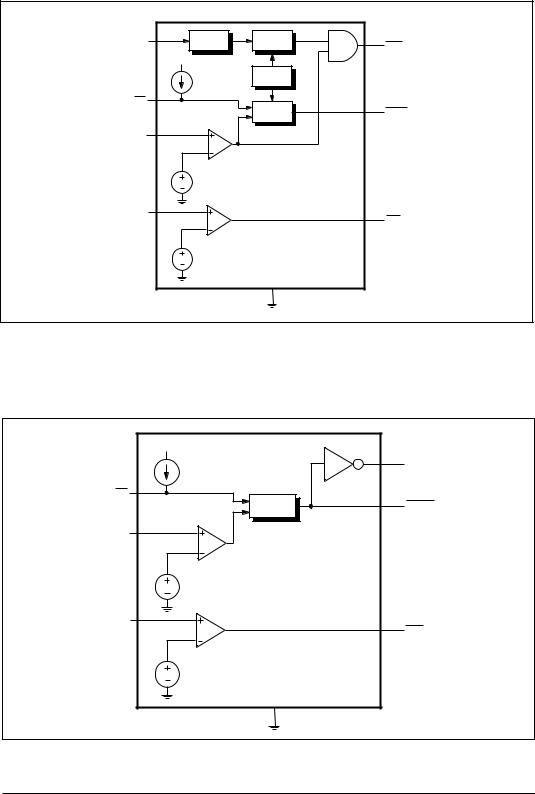
WDI |
WATCHDOG |
WATCHDOG |
|
TRANSITION |
|
||
TIMER |
WDO |
||
|
DETECTOR |
|
|
|
VCC |
|
|
|
|
TIMEBASE FOR |
|
|
250 A |
RESET AND |
|
|
WATCHDOG |
|
|
MR |
|
|
|
|
|
RESET |
RESET/RESET* |
|
|
GENERATOR |
|
VCC |
|
|
|
|
4.65V |
|
|
|
(4.40V for the SP706 and SP813M) |
|
|
PFI |
|
|
PFO |
|
|
|
|
|
1.25V |
|
SP705 |
|
|
SP706 |
|
|
|
|
|
|
|
|
SP813L |
|
|
|
SP813M |
|
|
GND |
* For the SP813L/813M only |
Figure 2. Internal Block Diagram for the SP705/706/813L/813M
VCC |
|
250 A |
RESET |
|
|
MR |
|
RESET |
RESET |
GENERATOR |
|
VCC |
|
4.65V |
|
(4.40V for the SP708) |
|
PFI |
PFO |
|
|
1.25V |
|
|
SP707 |
|
SP708 |
GND |
|
Figure 3. Internal Block Diagram for the SP707/708
SP705DS/09 |
SP705 Low Power Microprocessor Supervisory Circuits |
© Copyright 2000 Sipex Corporation |
5

Figure 4A. Power-Fail Comparator De-assertion
Response Time.
+5V |
|
|
|
VCC = +5V |
|
|
TA = +25 C |
|
PFI |
PFO |
|
|
|
|
+1.25V |
30pF |
1KΩ |
Figure 4B. Circuit for the Power-Fail Comparator Deassertion Response Time.
+5V
VCC = +5V
TA = +25 C
1KΩ
PFI
PFO
+1.25V 30pF
Figure 5A. Power-Fail Comparator Assertion Response |
Figure 5B. Circuit for the Power-Fail Comparator |
Time. |
Assertion Response Time. |
Figure 6A. SP705/707 RESET Output Voltage vs. Supply Voltage.
VCC |
|
TA = +25oC |
|
VCC |
2KΩ |
|
|
RESET |
RESET |
|
|
|
330pF |
GND |
|
Figure 6B. Circuit for the SP705/707 RESET Output Voltage vs. Supply Voltage.
SP705DS/09 |
SP705 Low Power Microprocessor Supervisory Circuits |
© Copyright 2000 Sipex Corporation |
6
 Loading...