


Sipex Corporation SPX1117M3, SPX1117M3-1.5, SPX1117M3-2.5, SPX1117M3-3.0, SPX1117U-2.5 Datasheet
...
|
SPX1117 |
|
800mA Low Dropout Regulator |
FEATURES |
APPLICATIONS |
• Guaranteed 800mA Output |
• Portable/ Palm Top / Notebook Computers |
• Three Terminal Adjustable Or Fixed 1.5V, 2.5V, 3V, 3.3V & 5V |
• Battery Chargers |
• Very Low Quiescent Current |
• Disk Drives |
• Low Dropout Voltage Of 1.2 Volts At Full Load |
• Portable Consumer Equipment |
• Extremely Tight Load And Line Regulation |
• Portable Instrumentation |
• Very Low Temperature Coefficient |
• SMPS Post-Regulator |
•Logic-Controlled Electronic Shutdown
•Internal Overcurrent Limiting & Thermal Overload Protection
•Surface Mount Package SOT-223, TO-252, TO-220, SOT-89, TO-263, & SO-8
PRODUCT DESCRIPTION
The SPX1117 is a low power positive-voltage regulator designed to meet 800mA output current. This device is an excellent choice for use in battery-powered applications. The SPX1117 features very low quiescent current and very low dropout voltage of 1.2V at a full load and lower as output current decreases. SPX1117 is available as an adjustable or fixed 1.5V, 2.5V, 3.0V, 3.3V, and 5.0V output voltages.
The SPX1117 is offered in a 3-pin surface mount package SOT-223, TO-252, TO-220 and TO-263. The output capacitor of 10 F or larger is needed for output stability of SPX1117 as required by most of the other regulator circuits.
PIN CONNECTIONS
|
8-Pin Surface Mount (S) |
TO-220-3 (U) |
SOT-223 (M3) |
TO-263-3 (T) |
TO-252 (R) |
|||||||||||
GND |
1 |
8 |
VIN |
|
|
|
|
|
|
|
|
|
|
|
|
|
N/C |
2 |
7 |
VIN |
|
|
|
SPX1117 |
|
SPX1117 |
|
SPX1117 |
|||||
V |
3SPX1117 6 |
V |
SPX1117 |
1 |
2 |
3 |
1 |
|
2 |
3 |
1 |
2 |
3 |
|||
|
|
|
|
|||||||||||||
OUT |
|
|
IN |
1 |
2 |
3 |
|
|
|
|
|
|
|
|
|
|
VOUT |
|
|
|
ADJ/GND |
VOUT |
VIN |
|
|
|
|
|
|
|
|||
4 |
5 |
N/C |
|
|
|
|
|
|
|
ADJ/GND |
|
|
||||
|
|
|
|
|
|
|
Top View |
|
|
|
|
|
VOUT |
VIN |
||
|
|
Top View |
|
|
|
|
|
|
|
|
|
|
||||
|
|
|
|
|
|
|
|
|
ADJ/GND |
VOUT |
VIN |
|
|
|
||
|
|
|
|
|
|
|
|
|
|
|
|
|
|
|
||
|
|
|
|
ADJ/GND |
VOUT |
VIN |
|
|
|
|
Top View |
|
Front View |
|||
|
|
|
|
|
|
|
|
|
|
|
|
|
|
|||
Front View
Rev. 10/20/00

SPX1117
ABSOLUTE MAXIMUM RATINGS
Power Dissipation.......................................... |
Internally Limited |
Lead Temp. (Soldering, 5 Seconds) ................................ |
260°C |
Storage Temperature Range ............................ |
-65° to +150°C |
Operating Junction Temperature Range |
|
SPX1117................................................ |
-40C° to +125°C |
Input Supply Voltage ...................................... |
-20V to +20V |
ESD Rating ............................................................ |
2KV Min |
ELECTRICAL CHARACTERISTICS at VIN = VOUT +1, Ta=25°C, CL =3.3 f, unless otherwise specified. Limits in Boldface apply over the full operating temperature range.
Parameter |
Conditions |
Typ |
SPX1117 |
Units |
|
Min |
Max |
||||
1.5V Version |
|
|
|
|
|
Output Voltage |
IOUT = 10mA, VIN = 4.85V |
1.500 |
1.485 |
1.515 |
V |
|
0≤IOUT≤800mA, 4.25≤VIN≤10V |
|
1.470 |
1.530 |
|
2.5V Version |
|
|
|
|
|
Output Voltage |
IOUT = 10mA, VIN = 4.85V |
2.500 |
2.475 |
2.525 |
V |
|
0≤IOUT≤800mA, 4.25≤VIN≤10V |
|
2.450 |
2.550 |
|
3.0V Version |
|
|
|
|
|
Output Voltage |
IOUT = 10mA, VIN = 4.85V |
3.000 |
2.970 |
3.030 |
V |
|
0≤IOUT≤800mA, 4.75≤VIN≤10V |
|
2.940 |
3.060 |
|
3.3V Version |
|
|
|
|
|
Output Voltage |
IOUT = 10mA, VIN = 5.0V |
3.300 |
3.267 |
3.333 |
V |
|
0≤IOUT≤800mA, 4.75≤VIN≤10V |
|
3.234 |
3.366 |
|
5.0V Version |
|
|
|
|
|
Output Voltage |
IOUT = 10mA, VIN = 7.0V |
5.000 |
4.950 |
5.050 |
V |
|
0≤IOUT≤800mA, 6.50≤VIN≤12V |
|
4.900 |
5.100 |
|
All Output Options |
|
|
|
|
|
Reference Voltage |
IOUT = 10mA, (VIN – VOUT) = 2V |
1.250 |
1.238 |
1.262 |
V |
|
10≤ IOUT≤800mA, 1.4≤(VIN -VIN) ≤10V |
|
1.225 |
1.270 |
|
Output Voltage |
(Note 1) |
|
|
0.05 |
% |
Temperature Stability |
|
|
|
|
|
Line Regulation |
4.50V ≤VIN≤12V, VOUT = 3.00, IOUT = 0 |
1.00 |
|
7.00 |
mV |
|
4.80V ≤VIN≤12V, VOUT = 3.30, IOUT = 0 |
1.00 |
|
7.00 |
|
|
6.50V ≤VIN≤15V, VOUT = 5.00, IOUT = 0 |
1.00 |
|
10.00 |
|
Load Regulation |
0≤IOUT≤800mA, VIN = 4.50V, VOUT = 3.00 |
1.00 |
|
12.00 |
mV |
|
0≤IOUT≤800mA, VIN = 4.80V, VOUT = 3.30 |
1.00 |
|
12.00 |
|
|
0≤IOUT≤800mA, VIN = 6.50V, VOUT = 5.00 |
1.00 |
|
15.00 |
|
Dropout Voltage |
IL = 100mA |
1.00 |
|
1.10 |
V |
( Note 2) |
IL = 500mA |
1.05 |
|
1.15 |
|
|
IL = 800mA |
1.10 |
|
1.20 |
|
Quiescent Current |
4.25V ≤VIN≤6.5V |
5.00 |
|
10.00 |
mA |
Current Limit |
(VIN-VOUT) = 5V |
1000 |
|
1200 |
mA |
Thermal Regulation |
25°C,30mS Pulse |
0.01 |
|
0.1 |
%/W |
Ripple Rejection |
fRIPPLE = 120Hz, (Vin-VOUT) = 3V, |
60 |
|
75 |
dB |
|
VRIPPLE = 1Vp-p |
|
|
|
|
Long Term Stability |
125°C, 1000Hrs |
|
|
0.03 |
% |
RMS Output Noise |
% of Vout, 10Hz≤f≤10kHz |
|
|
0.003 |
% |
Thermal Resistance |
Junction to case, at tab |
|
|
15 |
°C/W° |
|
|
|
|
|
|
Note 1: Output temperature coefficient is defined as the worst case voltage change divided by the total temperature range
Note 2: Dropout voltage is defined as the input to output differential at which the output voltage drops 100mV below its nominal value measured at 1V differential at very low values of programmed output voltage, the minimum input supply voltage of 2V ( 2.3V over temperature) must be taken into account.
Note 3: Thermal regulation is defined as the change in output voltage at a time T after a change in power dissipation is applied. excluding load or line regulation effect.
Rev. 10/20/00
SPX1117
APPLICATION NOTES EXTERNAL CAPACITOR
To ensure the stability of the SPX1117 an output capacitor of at least 10µF (tantalum)or 50µF (aluminum) is required. The value may change based on the application requirements on the output load or temperature range. The capacitor equivalent series resistance (ESR) will effect the SPX1117 stability. The value of ESR can vary from the type of capacitor used in the applications. The recommended value for ESR is 0.5Ω. The output capacitance could increase in size to above the minimum value. The larger value of output capacitance as high as 100µF can improve the load transient response.
SOLDERING METHODS
The SPX1117 SOT-223 package is designed to be compatible with infrared reflow or vapor-phase reflow soldering techniques. During soldering the non-active or mildly active fluxes may be used. The SPX1117 die is attached to the heatsink lead which exits opposite the input, output, and ground pins.
Hand soldering and wave soldering should be avoided since these methods can cause damage to the device with excessive thermal gradients on the package. The SOT-223 recommended soldering method are as follows: vapor phase reflow and infrared reflow with the component preheated to within 65°C of the soldering temperature range.
THERMAL CHARACTERISTICS
The thermal resistance of SPX1117 is 15°C/W from junction to tab and 31 °C/W from tab to ambient for a total of 46 °C/W from junction to ambient. The SPX1117 features the internal thermal limiting to protect the device during overload conditions. Special care needs to be taken during continuos load conditions the maximum junction temperature does not exceed 125 °C.
Taking the FR-4 printed circuit board and 1/16 thick with 1 ounce copper foil as an experiment (fig.1 & fig.2), the PCB material is effective at transmitting heat with the tab attached to the pad area and a ground plane layer on the backside of the substrate. Refer to table 1 for the results of the experiment.
The thermal interaction from other components in the application can effect the thermal resistance of the SPX1117. The actual thermal resistance can be determined with experimentation. SPX1117 power dissipation is calculated as follows:
PD = (VIN - VOUT)(IOUT)
Maximum Junction Temperature range:
TJ = Tambient (max) + PD* thermal resistance (Junction-to- ambient)
Maximum Junction temperature must not exceed the 125°C.
50 X 50 mm |
35 X 17 mm |
16 X 10 mm |
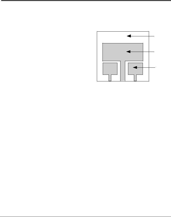
Fig. 1. Substrate Layout for SOT-223
Rev. 10/20/00
 Loading...