

Siemens SFH600 Datasheet

)
)
.
.
SFH600 SERIES
TRIOS* PHOTOTRANSISTOR
OPTOCOUPLER
FEATURES
• High Current Transfer Ratios
SFH600-0, 40 to 80%
SFH600-1, 63 to 125%
SFH600-2, 100 to 200%
SFH600-3, 160 to 320%
Dimensions in inches (mm)
3
248 (6.30)
256 (6.50)
12
Pin One ID
Anode
Cathode
1
2
6
Base
5
Collector
• Isolation Test Voltage (1 Sec.), 5300 VACRMS
• VCEsat 0.25 (£0.4) V, IF=10 mA, IC=2.5 mA
• High Quality Premium Device
• Long Term Stability
• Storage Temperature, –55∞ to +150∞C
• Underwriters Lab File #E52744
V
• VDE 0884 Available with Option 1
DE
DESCRIPTION
The SFH600 is an optocoupler with a GaAs LED
emitter which is optically coupled with a silicon planar phototransistor detector. The component is
packaged in a plastic plug-in case, 20 AB DIN
41866.
The coupler transmits signals between two electri-
.039
(1.00)
.018 (0.45)
.022 (0.55)
Min.
typ.
4
5
6
.335 (8.50)
.343 (8.70)
.130 (3.30)
.150 (3.81)
4°
.020 (.051) min.
.031 (0.80)
.035 (0.90)
.100 (2.54) typ.
NC
3
.300 (7.62)
18° typ.
.010 (.25)
.014 (.35)
.300 (7.62)
.347 (8.82)
typ.
4
Emitter
.110 (2.79
.150 (3.81
cally isolated circuits. The potential difference
between the circuits to be coupled is not allowed to
Characteristics
exceed the maximum permissible insulating voltage.
Maximum Ratings
Emitter
Reverse Voltage................................................. 6 V
DC Forward Current......................................60 mA
Surge Forward Current (t
=10 µs).................. 2.5 A
p
Total Power Dissipation.............................. 100 mW
Detector
Collector-Emitter Voltage................................ 70 V
Emitter
Forward Voltage V
Breakdown Voltage V
Reverse Current I
Capacitance C
Thermal Resistance R
Emitter-Base Voltage ....................................... 7 V
Collector Current...........................................50 mA
Collector Current (t=1 ms)..........................100 mA
Power Dissipation...................................... 150 mW
Package
Isolation Test V oltage (between emitter and
detector referred to climate DIN 40046,
part 2, Nov. 74) (t=1 sec.)..............5300 VAC
RMS
Creepage......................................................≥7 mm
Clearance
.......................................................... ≥
7 mm
Isolation Thickness between Emitter &
Detector.....................................................
Comparative Tracking Index per
DIN IEC 112/VDE0303, part 1........................175
≥
0.4 mm
Detector
Capacitance
Collector-Emitter
Collector-Base
Emitter-Base
Thermal Resistance R
Package
Saturation Voltage,
Collector-Emitter V
Coupling Capacitance C
(T
A
=25°C)
Symbol Unit Condition
F
BR
R
O
THJamb
C
CE
C
CB
C
EB
THJamb
CEsat
IO
1.25 (≤1.65) V IF=60 mA
6VI
≥
0.01 (≤10)
25 pF VF=0 V, f=1 MHz
750
5.2
6.5
9.5
500
0.25 (≤0.4) V
0.6 pF VIO=0, f=1 MHz
µ
AV
°
C/W
pF f=1 MHz
°
C/W
=10 µA
R
=6 V
R
VCE=5 V
VCB=5 V
VEB=5 V
IF=10 mA,
IC=2.5 mA
Isolation Resistance
V
=500 V, TA=25°C
IO
VIO=500 V, TA=100°C
...................................≥
.................................≥
1012
1011
Ω
Ω
*TRIOS
—TRansparent IOn Shield
Storage Temperature Range........–55°C to +150°C
Ambient Temperature Range....... –55
Junction Temperature....................................100
°
C to +100°C
°
C
Soldering Temperature (max. 10 s, dip
soldering: distance to seating plane
1.5 mm)....................................................260°C
≥
5–1
This document was created with FrameMaker 4.0.4
Current Transfer Ratio and Collector-Emitter Leakage Current
V
V
by dash number
-0 -1 -2 -3 Unit
IC/IF at VCE=5 V
(IF=10 mA) 40-80 63-
125
IC/IF at VCE=5 V
(IF=1 mA) 30
(>13)
45
(>22)
Collector-Emitter
Leakage Current
(VCE=10 V)
(I
)
CEO
2 (≤
35)
2 (≤
35)
100200
70
(>34)
2 (≤
35)
160320
90
(>56)
5 (≤
70)
%
%
nA
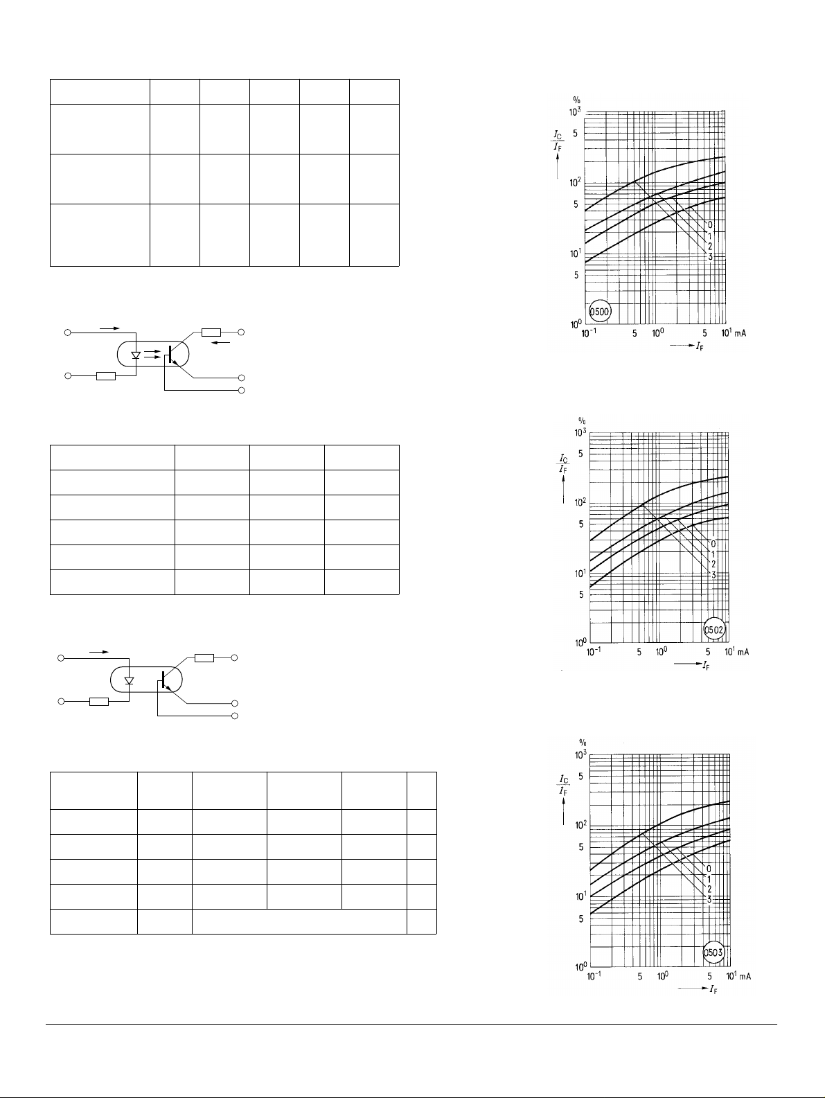
Figure 3. Current transfer ratio versus
diode current
(T
=–25°C, V
A
=5 V) IC/IF=f (IF)
CE
Figure 1. Linear operation
I
F
(without saturation)
RL=75 Ω
I
C
47 Ω
IF=10 mA, VCC=5 V, TA=25 °C, Typical
Load Resistance R
Turn-On Time t
Rise Time t
Turn-Off Time t
Fall Time t
Cut-off Frequency F
Figure 2. Switching operation
I
F
L
ON
R
OFF
f
CO
(with saturation)
1 KΩ
V
=5
CC
75
3.2
2.0
3.0
2.5
250 kHz
=5
V
CC
Figure 4. Current transfer ratio versus
diode current (T
I
=f (IF)
C/IF
Ω
µ
s
µ
s
µ
s
µ
s
=0°C, VCE=5 V)
A
47 Ω
Typical
Turn-On Time t
Rise Time t
Turn-Off Time t
Fall Time t
ON
R
OFF
F
V
CESAT
-0
(I
=20 mA)
F
-1 and -2
(IF=10 mA)-3(IF=5 mA)
3.7 4.5 5.8
2.5 3.0 4.0
19 21 24
11 12 14
0.25 (≤0.4) V
5–2
Figure 5. Current transfer ratio versus
diode current (T
I
=f (IF)
F
µ
s
µ
s
µ
s
µ
s
=25°C, VCE=5 V)IC/
A
SFH600
 Loading...