

Page 1
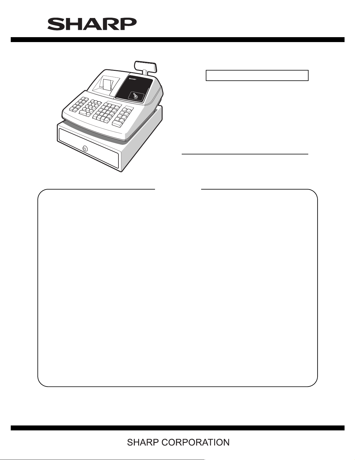
SERVICE MANUAL
MODEL XE-A203
CONTENTS
CODE : 00Z
LEAD-FREE SOLDER MODEL
XEA203USME
ELECTRONIC
CASH REGISTER
(U and A version)
■ LEAD-FREE SOLDER
CHAPTER 1. SPECIFICATIONS . . . . . . . . . . . . . . . . . . . . . . . . . . . . 1
CHAPTER 2. OPTIONS . . . . . . . . . . . . . . . . . . . . . . . . . . . . . . . . . . . 5
CHAPTER 3. MASTER RESET AND PROGRAM RESET. . . . . . . . . 6
CHAPTER 4. HARDWARE DESCRIPTION . . . . . . . . . . . . . . . . . . . . 6
CHAPTER 5. TEST FUNCTION . . . . . . . . . . . . . . . . . . . . . . . . . . . . 12
CHAPTER 6. CIRCUIT DIAGRAM AND PWB LAYOUT . . . . . . . . . 15
Parts marked with "!" are important for maintaining the safety of the set. Be sure to replace these parts with specified
ones for maintaining the safety and performance of the set.
This document has been published to be used
SHARP CORPORATION
for after sales service only.
The contents are subject to change without notice.
Page 2
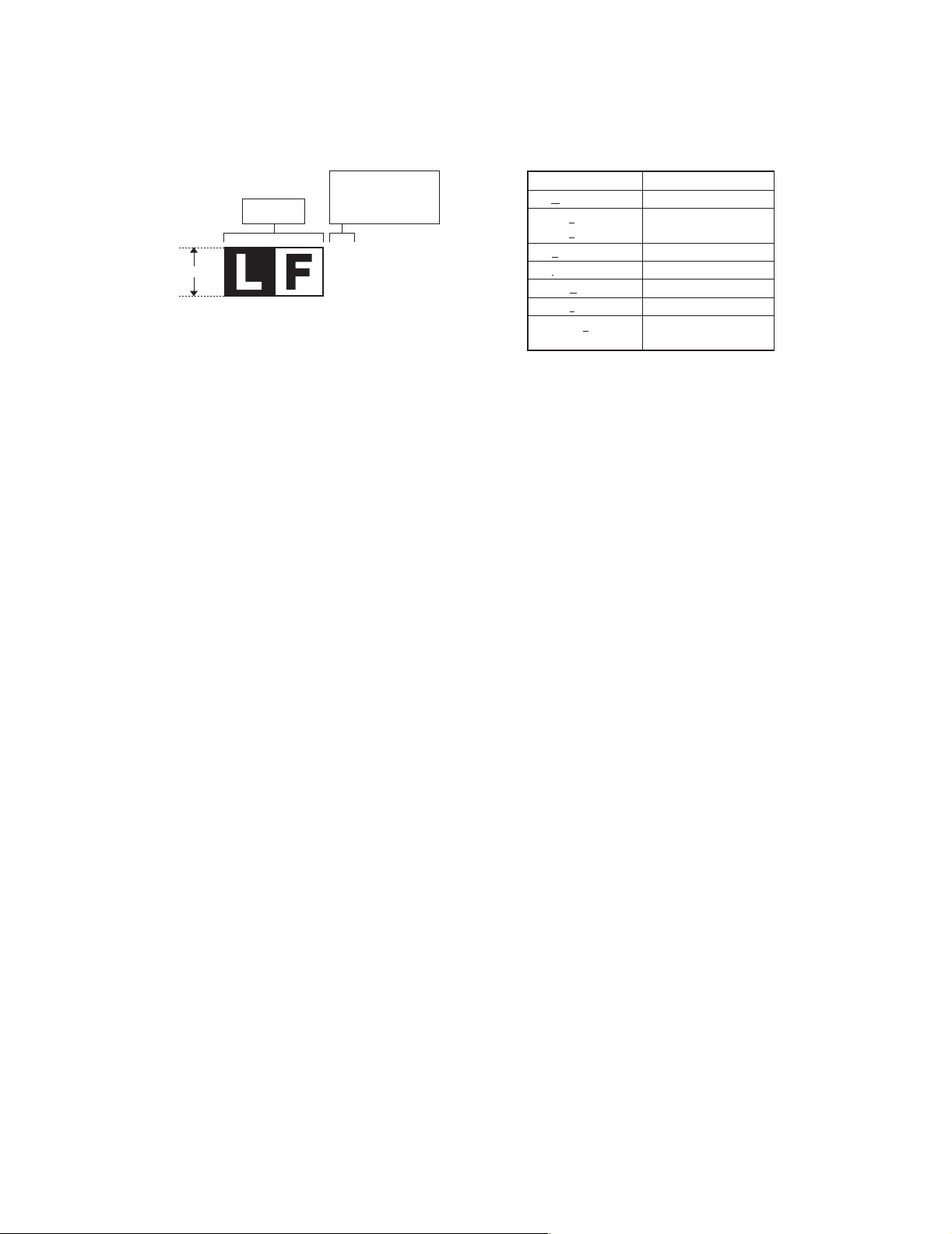
■ LEAD-FREE SOLDER
The PWB’ s of this model employs lead-free solder. The “LF” marks indicated on the PWB’s and the Service Manual mean “Lead-Free” solder. The
alphabet following the LF mark shows the kind of lead-free solder.
Example:
<Solder composition code of lead-free solder>
Solder composition
Sn-Ag-Cu
Sn-Ag-Bi
Sn-Ag-Bi-Cu
Sn-Zn-Bi
Sn-In-Ag-Bi
Sn-Cu-Ni
Sn-Ag-Sb
Bi-Sn-Ag-P
Bi-Sn-Ag
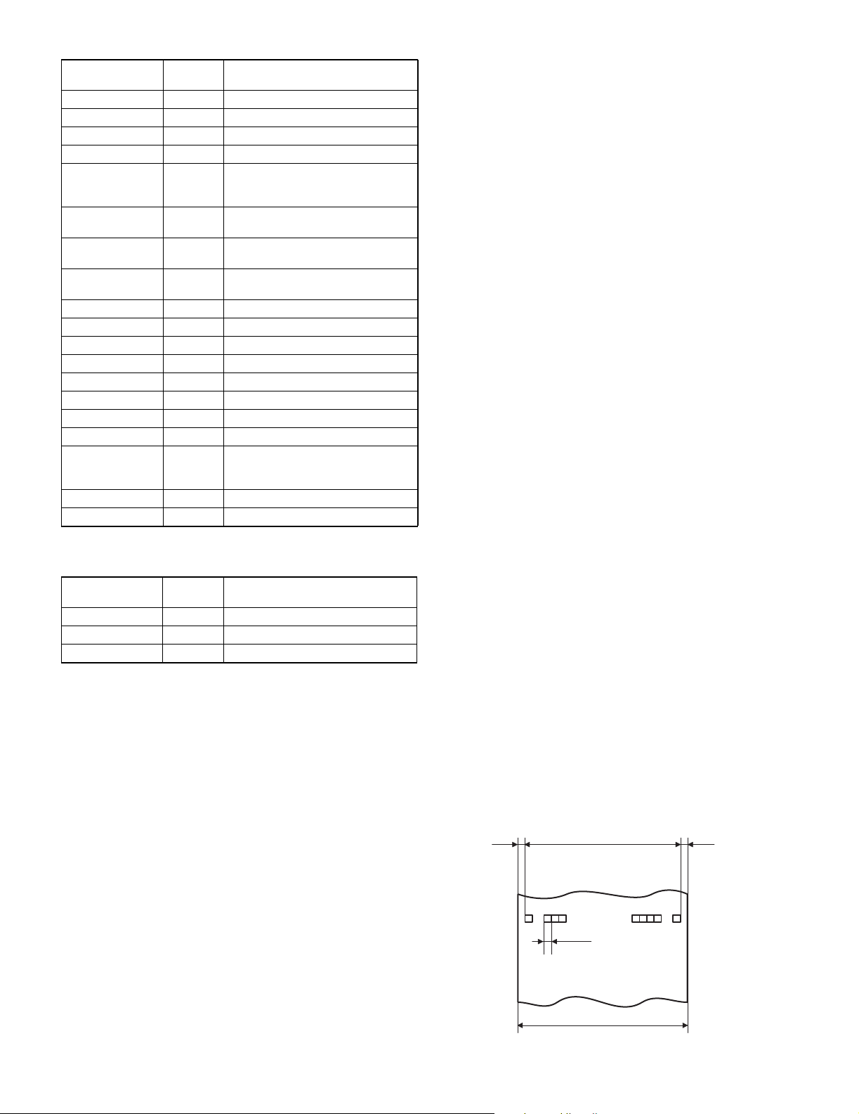
5mm
Lead-Free
Solder composition
code (Refer to the
table at the right.)
a
(1) NOTE FOR THE USE OF LEAD-FREE SOLDER THREAD
When repairing a lead-free solder PWB, use lead-free solder thread. Never use conventional lead solder thread, which may cause a breakdown or an accident.
Since the melting point of lead-free solder thread is about 40°C higher than that of conventional lead solder thread, the use of the exclusive-use soldering iron is recommendable.
(2) NOTE FOR SOLDERING WORK
Solder composition code
a
b
z
i
n
s
p
Since the melting point of lead-free solder is about 220°C, which is about 40°C higher than that of conventional lead solder, and its soldering capacity is inferior to
conventional one, it is apt to keep the soldering iron in contact with the PWB for longer time. This may cause land separation or may exceed the heat-resistive temperature of components. Use enough care to separate the soldering iron from the PWB when completion of soldering is confirmed.
Since lead-free solder includes a greater quantity of tin, the iron tip may corrode easily. Turn ON/OFF the soldering iron power frequently.
If different-kind solder remains on the soldering iron tip, it is melted together with lead-free solder. To avoid this, clean the soldering iron tip after completion of soldering work.
If the soldering iron tip is discolored black during soldering work, clean
and file the tip with steel wool or a fine filer.
XE-A203U/XE-A203A LEAD-FREE SOLDER
Page 3
CHAPTER 1. SPECIFICATIONS
1. APPEARANCE
Front view Rear view
Customer display
Operator display
Printer cover
Receipt paper
Keyboard
Drawer
Drawer lock
(Pop-up type)
Power cord
Mode switch
Printer
Take-up spool
Print roller arm
Print roller
release lever
Inner cover
Paper roll cradle
Paper positioning guides
2. RATING
Model XE-A203
Dimensions 13.8 (W) x 16.9 (D) x 11.1 (H) in.
Weight 17.6 Ib (8 kg)
Power source 120V AC
Power consumption Stand-by 7.7 W
Working temperature 32 °F to 104 °F (0 °C to 40 °C)
(350 (W) x 430 (D) x 281 (H) mm)
±10%, 60 Hz
Operating 28 W (max.)
■Key names
KEY TOP DESCRIPTION
2 Paper feed key
RA Received-on account key
RCPT/PO Receipt print/Paid-out key
VOID Void key
ESC Escape key
CONV Conversion key
%1, %2 Percent 1and 2 key
RFND Refund key
- Discount key
@/FOR Multiplication key
USB portSD card slot
• Decimal point key
CL Clear key
0-9,00 Numeric Keys
PLU/SUB PLU/Sub-department key
DEPT# Department code entry key
DEPT SHIFT Department shift key
CLK# Clerk code entry key
Dept1-32 Department keys
TAX Tax k e y
Tax 1 SHIFT Tax 1 shift key
Tax 2 SHIFT Tax 2 shift key
AUTO Automatic sequence key
CHK Check key
CH Charge key
MDSE SBTL Merchandise subtotal key
#/TM/SBTL Non-add code/Time display/Subtotal key
CA/AT/NS Total/Amount tender/No Sale key
4. MODE SWITCH
3. KEYBOARD
1) KEYBOARD LAYOUT
Type Normal keyboard
Key position STD/MAX 53
Key pitch 19 (W) x 19 (H) mm
Key layout Fixed type
2) KEY LIST
■Keyboard layout
PLU
CL
00
/SUB
4
3
2
1
RCPT
/PO
VOID
DC
ESC
BS
CONV
NUMBER
–
RFND
%1RA
%2
SHIFT
SPACE
@/
FOR
•
789
456
123
0
Note: The small characters on the bottom or lower right in each key
indicates functions or characters which can be used for character
entries for text programming.
DEPT
DEPT
#
A
20
B
8
19
C
7
18
D
6
17
E
5
CLK
SHIFT
F
24
G
12
23
H
11
22
I
10
21
J
9
#
K
P
28
32
L
Q
16
27
31
M
R
15
26
30
N
S
14
25
29
O
T
13
AUTO
TAX
TAX1
SHIFT
CHK
MDSE
SBTL
X
U
TAX2
SHIFT
Y
V
CH
Z
W
#/TM
SBTL
CA/AT/NS
XE-A203U/XE-A203A SPECIFICATIONS
1) LAYOUT
• Rotary type
MA
OP
REG
OP
X/Z
OFF
VOID
PGM
MGR
X
1/Z1
X2/Z2
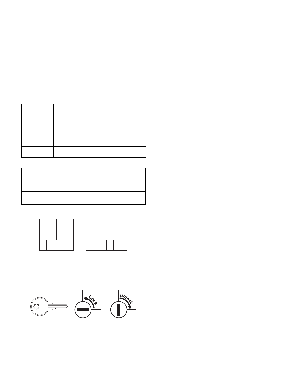
The mode switch can be operated by inserting one of the two supplied
mode keys - manager (MA) and operator (OP) keys. These keys can be
inserted or removed only in the “REG” or “OFF” position.
– 1 –
Manager key (MA)
Operator key (OP)
OPMA
Page 4
The mode switch has these settings:
OFF: This mode locks all register operations. (AC power turns off.)
No change occurs to register data.
OP X/Z: To take individual clerk X or Z reports, and to take flash reports.
It can be used to toggle receipt state “ON” and “OFF” by
pressing he [RCPT/PO] key.
REG: For entering sales.
PGM: To program various items.
VOID
: Enters into the void mode. This mode allows correction after
finalizing a transaction.
MGR: For manager’s entries. The manager can use this mode for
an override entry.
X1/Z1: To take the X/Z report for various daily totals.
X2/Z2: To take the X/Z report for periodic (weekly or monthly) consol-
idation.
5. DISPLAY
1) OPERATOR DISPLAY
Display device: LED
Number of line: 1 line
Number of positions: 10 positions
Color of display: Yellow / Green
Character form: 7 segment + DP
Character size: Numeric 14.2 (H) x 7.9 (W) mm
Layout:
0.1.2.3.4.5.6.7.8.9.
2) CUSTOMER DISPLAY
Display device: LED
Number of line: 1 line
Number of positions: 7 positions
Color of display: Yellow / Green
Style: Pop up type
Character form: 7 segment + Dp
Character size: 14.2mm (H) x 7.9mm (W)
Layout:
3.4.5.6.7.8.9.
Operator display
PLU/SUB
DEPT REPEAT
RCPT
OFF
DC
Clerk code
NUMBERSHIFT
Customer display (Pop-up type)
Amount: Appears in the far-right eight (max.) positions. When the
amount is negative, the minus symbol “-” appears before the
amount.
Number of repeats for repetitive registrations:
The number of repeats is displayed, starting at “2” and incremental with each repeat. When you have registered ten
times, the display will show “0.” (2 3 3
.....
9 3 0 3 1 3 2
Receipt function status:
The indicator “_” appears in the RCPT OFF position when
the receipt function is in the OFF status.
Time: Appears in the far-right six positions (hour-minute - “ ” or
hour-minute - “ ”) in the OP X/Z, REG, or MGR mode. “ ”
is displayed in the morning (AM), and “ ” in the afternoon
(PM). In the REG or MGR mode, press the [#/TM/SBTL] key
to display the time.
■Machine state symbols
: Appears during programming.
: Appears when an error is detected.
: Appears when the subtotal is displayed or when the amount
tendered is smaller than the sales amount.
: Appears when the [CONV] key is pressed to calculate a subto-
tal in foreign currency.
: Appears when a transaction is finalized by pressing the [CA/AT/
NS], [CHK] or [CH] key.
: Appears when the change due amount is displayed.
: May appear in the far-left three positions at the timing of key
entry when the electronic journal (EJ) memory is full. (Depending on programming.)
: Appears when the voltage of the installed batteries is under the
required level. You must replace with new ones within two days.
: Appears when the batteries are not installed, or the installed
batteries are dead. You must replace with new ones immediately.
: May appear right below the eighth and ninth places at the timing
of finalization of a transaction when the electronic journal (EJ)
memory is nearly full.
Also appears right below the tenth place when power save
mode is effective.
: Appears when the print roller arm is not locked.
: Appears when the paper is not set or out.
...
)
XE-A203U/XE-A203A SPECIFICATIONS
– 2 –
Page 5
Segment
Display
position
Amount 1-8
Minus sign 2-10 -: Floating
Error 8-10 Exx: xx = error code
PGM Mode 10 P
CASH, CHECK,
CHARGE
SUB TOTAL/
short tender
Change 10 C: Light up whenever the change due
Currency
Conversion
Department 9-10 No zero-suppressed
PLU 7-10 No zero-suppressed
Repeat 8 Endless count, starting from 2.
Receipt OFF 9 _
DC _: Double size character entry status
SHIFT _: Shift character entry status
NUMBER _: Number character entry status
Clerk No. 2, 3 -xx-: clerk number
EJ FULL 8-10 E-E: Light up when EJ memory is
Low Battery 10 L:
No Battery 10
10 F: Light up when a registration is
10 o
10 c: Light up whenever the foreign
finalized by depressing [CASH],
[CHECK], [CHARGE] key
amount appears in the display.
amount appears in the display.
:
L
Description
FULL at the timing of key entry
(by PGM selection).
6. PRINTER
1) Printer
• Part number : M-T53II
• NO. of station : 1 (Receipt or journal)
• Validation : No.
• Printing system : Line thermal
• No. of dot : 288 dots
• Dot pitch : Horizontal 0.167mm
Vertical 0.174mm
• Font : 10 dots (W) x 24 dots (H)
• Printing capacity : max. 24 characters
• Character size : 1.67mm (W) x 4.17mm (H) at 10 x 24 dots
• Print pitch : Column distance 2.0mm
Row distance 5.21mm
• Max. Print speed : Approximate 60mm/s (Approximate 12 l/s)
•
Max. Paper feed speed
(Manual feed) : Approximate 40mm/s (Approximate 12 l/s)
• Reliability : Mechanism LIFE 6 million lines used to
• Paper end sensor : Set up
• Cutter : No
• Near end sensor : No
: Approximate 60mm/s (Approximate 12 l/s)
high-quality thermal paper
Decimal Point
Display
position
Decimal point 7-1
TA B 4- 1
EJ near full 8, 9 (by PGM selection)
Description
2) Paper
• Paper roll dimension:
• Paper quality: High-quality thermal paper
57.5m 0.5mm in width
Max. 80mm in diameter
paper thickness: 0.06 to 0.08mm
Nihon seisi thermal paper : TF50KS-E
Oil thermal paper: PD150R,
3) Logo stamp
• No
4) Printing area
Number of thermal head heater elements 288 dots
(4.75) (4.75)48 (288 dots)
print area
(max.24 characters)
0.167
PD160R
XE-A203U/XE-A203A SPECIFICATIONS
– 3 –
57.5±0.5
(Paper dimension)
(units : mm)
Page 6
7. DRAWER
8. USB PORT
[OUTLINE]
• Standard equipment: Yes (1)
• Max. number of additional drawers: 1
• The drawer consists of:
1) Drawer box (outer case) and drawer
2) Money case
3) Coin case
4) Lock (attached to the drawer)
[SPECIFICATION]
1) DRAWER BOX AND DRAWER
Type SEC SECL
Model name of
the drawer box
Size (mm) 330(W) x 418(D) x 98(H)
Material Plastic
Bell —
Release lever Standard equipment: situated at the bottom
Drawer open
sensor
2)MONEY CASE
Type SEC SECL
Separation from the drawer Disallowed
Separation of the bill compartments
from the coin compartments
Bill separator —
Number of compartments 4B/5C 5B/6C
Layout:
3) Drawer Lock Key
This key locks and unlocks the drawer. To lock it, turn 90 degrees counterclockwise. To unlock it, turn 90 degrees clockwise.
SJ415 SJ423
355(W) x 423(D) x 110(H)
—
Allowed
4B/5C (U version) 5B/6C (A version)
[DEVICE]
USB B Type
[OUTLINE]
This ECR has 1 port.
This is used in order to connect with a personal computer.
[SPECIDICATIONS]
1) Transmission tate
USB 2.0 Full Speed Max. 12Mbps
2) Connector
USB B Type
3) Pin assign
1Pin 5V
2Pin -D
3Pin +D
4Pin GND
9. BATTERY
1) MEMORY BACK UP BATTERY
For memory back up, the dry battery AA (3 pieces) are needed.
1. Memory holding time:
Approximate 1 year after New dry batteries are inserted.
2. Battery exchange method:
When the low battery symbol “L” lights up, batteries (3 pieces)
exhange by the following method, with 2 days.
1) Power on the ECR.
2) Mode switch turn to “REG” mode.
3) Release the OLD dry batteries (3 pieces).
4) Insert the NEW dry batteries (3 pieces).
5) Confirm the low battery symbol “L” lights off.
2) LOW BATTERY
Low battery indication will appear on the left side of display when the
battery voltage is low.
CASE 1: When any numeric entry & any item entry is not done or just
after finalization.
The machine can indicate the low battery condition. (Always)
CASE 2: When numeric entry or item entry is done.
Battery condition will not appear.
Exceptionally, when the power is restored after a power failure, the
low battery condition will appear on the display only when the battery is low.
And the indicator will disappear after any key entry.
XE-A203U/XE-A203A SPECIFICATIONS
– 4 –
Page 7
[Display sample]
“ 0.00”: Battery is OK.
“L 0.00”: Low battery (You have to change the batteries.)
“
L 0.00”: No battery (You have to change the batteries immediately.)
After finalization
“F 12.34”: Battery is OK.
“L 12.34”: Low battery. (“L” indicate instead of “F”.)
L 12.34”: No battery. (“L” indicate instead of “F”.)
“
Note: “NO BATTERY”: When the “NO BATTERY” is display, the mas-
ter reset is executed at the timing of “POWER
ON” after the “POWER OFF”.
CHAPTER 2. OPTIONS
1. OPTIONS (NONE)
10. SD MEMORY CARD
[Device]
SD Card (Version. 1.01)
[Outline]
XE-A203U has a SD Memory Card slot.
[Specidications]
1) Variable clock rate : 0 - 25 MHZ
2) Other commands and memory access : 2.7 - 3.6V
3) Bus Protocol : SPI Bus
4) Correspondence capacity : 32MB - 512MB
5) Recommended manufacturer : SanDisk
2. SERVICE OPTIONS (NONE)
3. SUPPLIES
NO NAME PARTS CODE PRICERANK DESCRIPTION
1 Thermal roll paper TPAPR6656RC05 BA 5 ROLLS/PACK
4. SPECIAL SERVICE TOOLS
NO NAME PARTS CODE PRICE RANK DESCRIPTION
1 USB Cable
CHAPTER 3. MASTER RESET AND PROGRAM RESET
1. MASTER RESETTING
Master resetting clears the entire memory and resumes initial values.
Master resetting can be accomplished by using the following procedure:
Procedure A: 1) Unplug the AC cord from the wall outlet or set the
mode switch to OFF Position.
2) Let the ECR be without the memory back up battery.
3) Wait over 1 muinite for discharging.
4) Set the mode switch to any position except OFF.
5) Plugin the AC cord to the wall outlet or turn the
mode switch from OFF Position to another position.
The master reset can also be accomplished in the following case.
In case power failure occurs when the machine has no battery
attached to it, the master reset operation is automatically performed
after the power has been restored.
(This is because if power failure occurs with no battery attached to
the machine, all the memories are lost and the machine does not
work properly after power recovery; this requires the master reset
operation.)
2. PROGRAM RESETTING
(INITIALIZATION)
This resetting resumes the initial program without clearing memory.
This resetting can be operated at below sequence in PGM mode.
Procedure: 1) Unplug the AC cord from the wall outlet.
2) Wait over 1 muinite for discharging.
3) Set the mode switch to the PGM position.
4) While holding down the FEED key, plugin the AC
cord to the wall outlet.
Note: In case power failure occurs when the machine has no battery
attached to it, the master reset operation is automatically
performed after the power has been restored.
XE-A203U/XE-A203A OPTIONS
– 5 –
Page 8

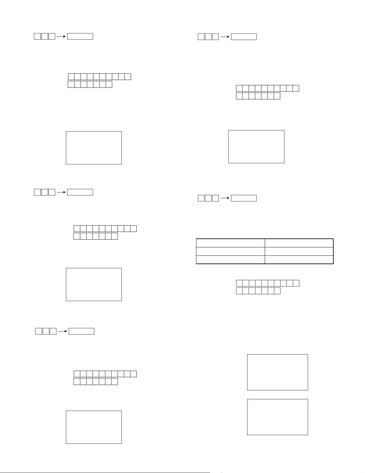
CHAPTER 4. HARDWARE DESCRIPTION
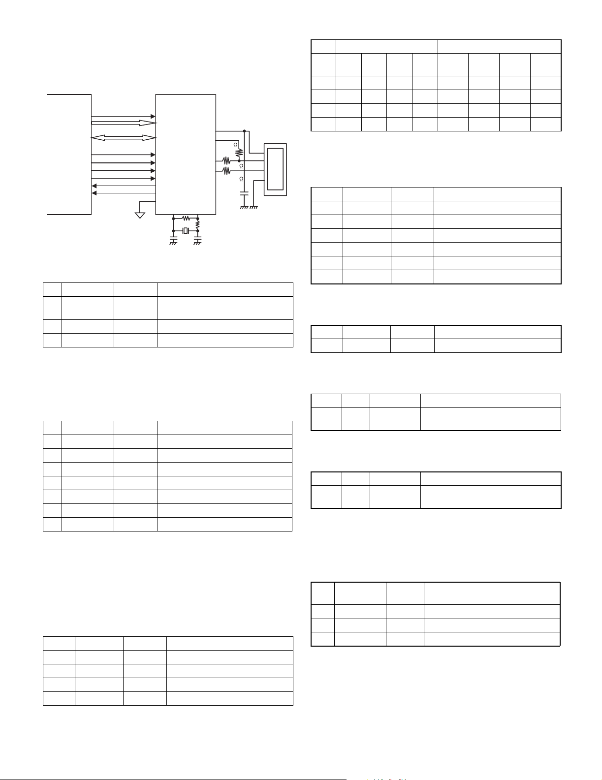
1. HARDWARE BLOCK DIAGRAM
12MHz
PRINTER
MT53II
DRY Battery
CPU
Renesus
M30624MWPD85FP
ROM 320KByte
RAM 24KByte
Decoder
74HC138 x 2
4 to 16
74H374
BUZZER
RESET IC
LV125
HCT04
S-RAM
128KByte
USB
Controller
M66291GP
SEG
Driver
DIG
Driver
KEY SCAN
KEY RETURN
POWER
5.8V
5.0V
3.3V
7.9V
23.8V
32.768kHz
DRAWER
Driver/Sensor
MOTOR
SD CARD
USB
Type B
LED
Front 10
PopUp 7
KEY
SWITCH
2. MEMORY MAP
1MByte mode/The CS area PM13 = 1 is selected.
CPU internal RAM: 24KByte 00400h-063FFh
External RAM: 128KByte 08000h-27000h
00000h
00400h
CPU internal RAM
24KByte 00400h-063FFh
063FFh
06400h
08000h External RAM
128KByte
27000h
28000h USB controller
(Area that can be used 124KByte)
/CS2
/CS1
<Main parts>
CPU: M30624MWP-D85FP (Renesus)
ROM 320KByte (MASK) RAM 24KByte
External RAM: 1Mbit (128K x 8)
CYPRESS CY62128BLL-70SXI
Printer: MT53II (EPSON)
USB controller: M66291GP (Renesus)
30000h Segment Latch Address
80000h
B0000h
CPU internal MASK ROM
320KByte B0000h-FFFFFh
FFFFFh
/CS0
XE-A203U/XE-A203A HARDWARE DESCRIPTION
– 6 –
Page 9

3. CPU PORT
PORT PIN No. Pin name Signal name I/O Initial value OFF MODE Function
P00 88 D0 D0 I/O H Out L DATE BUS D0
P01 87 D1 D1 I/O H Out L DATE BUS D1
P02 86 D2 D2 I/O H Out L DATE BUS D2
P03 85 D3 D3 I/O H Out L DATE BUS D3
P04 84 D4 D4 I/O H Out L DATE BUS D4
P05 83 D5 D5 I/O H Out L DATE BUS D5
P06 82 D6 D6 I/O H Out L DATE BUS D6
P07 81 D7 D7 I/O H Out L DATE BUS D7
P10 80 P10 KST0 O L In KEY DISPLAY (4 TO 16)
P11 79 P11 KST1 O L In KEY DISPLAY (4 TO 16)
P12 78 P12 KST2 O L In KEY DISPLAY (4 TO 16)
P13 77 P13 KST3 O L In KEY DISPLAY (4 TO 16)
P14 76 P14 IN2 O L Out L PAPER FEED MOTOR
P15 75 P15 IN1 O L Out L PAPER FEED MOTOR
P16 74 P16 ENA2 O L Out L PAPER FEED MOTOR
P17 73 P17 ENA1 O L Out L PAPER FEED MOTOR
P20 72 A0 A0 O H Out L ADDRESS BUS A0
P21 71 A1 A1 O H Out L ADDRESS BUS A1
P22 70 A2 A2 O H Out L ADDRESS BUS A2
P23 69 A3 A3 O H Out L ADDRESS BUS A3
P24 68 A4 A4 O H Out L ADDRESS BUS A4
P25 67 A5 A5 O H Out L ADDRESS BUS A5
P26 66 A6 A6 O H Out L ADDRESS BUS A6
P27 65 A7 A7 O H Out L ADDRESS BUS A7
P30 63 A8 A8 O H Out L ADDRESS BUS A8
P31 61 A9 A9 O H Out L ADDRESS BUS A9
P32 60 A10 A10 O H Out L ADDRESS BUS A10
P33 59 A11 A11 O H Out L ADDRESS BUS A11
P34 58 A12 A12 O H Out L ADDRESS BUS A12
P35 57 A13 A13 O H Out L ADDRESS BUS A13
P36 56 A14 A14 O H Out L ADDRESS BUS A14
P37 55 A15 A15 O H Out L ADDRESS BUS A15
P40 54 A16 A16 O H Out L ADDRESS BUS A16
P41 53 A17 A17 O H Out L ADDRESS BUS A17
P42 52 A18 A18 O H Out L ADDRESS BUS A18
P43 51 A19 A19 O H Out L ADDRESS BUS A19
P44 50 /CS0 /CS0 O H Out L SEGMENT LATCH
P45 49 /CS1 /CS1 O H Out L USB CONTROLLER
P46 48 /CS2 /CS2 O H Out H SRAM
P47 47 /CS3 (NU) O L Out L UNUSED
P50 46 /WR /WR O H Out L WRITE STROBE SIGNAL
P51 45 /BHE (NU) O L Out L UNUSED
P52 44 /RD /RD O H Out L READ STROBE SIGNAL
P53 43 BCLK (NU) O L Out L UNUSED
P54 42 /HLDA (NU) O L Out L UNUSED
P55 41 /HOLD /EMP I
P56 40 ALE (NU) O L Out L UNUSED
P57 39 /RDY /RDY I
P60 38 P60 DR1 O L Out L DRAWER DRIVE SIGNAL
P61 37 P61 SD_CLK O H Out L SD CLK
P62 36 P62 SD_RXD I
P63 35 P63 SD_TXD O H Out L SD TXD
-
-
-
In
In VCC PULL UP
In SD RXD
XE-A203U/XE-A203A HARDWARE DESCRIPTION
– 7 –
Page 10

PORT PIN No. Pin name Signal name I/O Initial value OFF MODE Function
P64 34 P64 SD_POWER# O H Out L SD POWER#
P65 33 P65 SD_CS# O H Out L SD CS#
P66 32 P66 SD_CD# I
P67 31 P67 SD_WP# I
-
-
In SD CD#
In SD WP#
P70 30 TXD2 DAT O L Out L PRINTER DATA OUT
P71 29 P71 (NU) O L Out L UNUSED
P72 28 CLK2 CLK O L Out L PRINTER CLOCK
P73 27 P73 (NU) O L Out L UNUSED
P74 26 P74 P74 I
P75 25 P75 P75 I
-
-
In FIXED TO L
In FIXED TO L
P76 24 P76 /RES_USB O L Out L USB RESET
P77 23 P77 /EPM CTRL O H Out L /EPM CONTROL SIGNAL WHEN IPL
P80 22 P80 BUZZER O L Out L BUZZER
P81 21 P81 MOTOR O L Out L PAPER TAKE UP MOTOR
P82 20 /INT0 POFF I
P83 19 /INT1 /DREQUSB I
P84 18 /INT2 /INTUSB I
P85 17 /NMI (NU) I
P86 11 XCOUT XCOUT I
P87 10 XCIN XCIN I
P90 7 P90 P90 I
P91 6 P91 P91 I
P92 5 P92 P92 I
P93 4 P93 P93 I
P94 3 P94 P94 I
P95 2 P95 P95 I
P96 1 P96 P96 I
P97 100 P97 P97 I
P100 97 AN0 P100 I
P101 95 AN1 P101 I
-
-
-
-
-
-
-
-
-
-
-
-
-
-
-
-
In POWER INTERRUPT
In USB DMA REQUEST
In USB INTERRUPT
In UNUSED
In 32.768kHz
In 32.768kHz
In KEY IN
In KEY IN
In KEY IN
In KEY IN
In KEY IN
In KEY IN
In KEY IN
In KEY IN
In HEAD TEMPERATURE MONITOR
In HEAD VOLTAGE MONITOR
P102 94 P102 /STB2 O H In PRINTER/STB2
P103 93 AN3 VBAT I
-
In BATTERY VOLTAGE
P104 92 P104 (NU) O L Out L UNUSED
P105 91 P105 VPON O L Out L PRINTER HEAD POWER
P106 90 P106 /LAT O H Out L PRINTER DATA LATCH
P107 89 P107 /STB1 O H In PRINTER/STB1
BYTE 8 BYTE I
CNVss 9 CNVss I
/RESET 12 /RESET I
-
-
-
In CONNECTED TO VDD
In NOMAL: L / BOOT: H
In RESET
Xout 13 Xout O Out CLOCK
Vss 14 Vss power CONNECTED TO GND
Xin 15 Xin I In CLOCK
Vcc 16 Vcc power CONNECTED TO VDD
Vcc 62 Vcc power CONNECTED TO VDD
Vss 64 Vss power CONNECTED TO GND
AVss 96 AVss power CONNECTED TO GND
Vref 98 Vref ref CONNECTED TO VDD
AVcc 99 AVcc power CONNECTED TO VDD
XE-A203U/XE-A203A HARDWARE DESCRIPTION
– 8 –
Page 11
4. USB PORT
One port for USB Port (Slave) is provided as a standard provision.
The Renesus-make USB general-use ASSP device M66291 is used.
The M66291 is mapped to the /CS1 area 28000h-29FFFh.
CPU
A0
A1-A6
D0-D7
/CS1
/RD
/WR
/RESUSB
/DREQUSB
/INTUSB
<CPU PORT>
No. CPU PORT Use signal Purpose
19 P83 (INT1)
18 P84 (INT2) /INTUSB USB interruption 0 request signal
P76 (TA3OUT)
24
/DREQUSB
/REUSB M66291 Reset control
M66291
D15/AD0
AD1-AD6
VBuss
D0-D7 TrON
CS
RD
D+
LWR
D/RESET
/Dreq0
24MHz
1.5k
1.0uF
1
3
27
2
4
27
USB
CONNECTOR
USB DMA channel 0 DMA request
signal
Vbus
D+
D-
GND
<DRIVE STEP>
Driver IC input (CPU output) Motor drive signal
STEP IN1 IN2 ENA1 ENA2
A
(OUT1)B (OUT3)
/A
(OUT2)
(OUT4)
1LLHH H H L L
2HLHH L H H L
3HHHH L L H H
4LHHH H L L H
6-2. HEAD CONTROL
HEAD : All 288dot, Width 0.167mm/dot (6dot/mm)
<CPU PORT>
Pin No. CPU PORT Use signal Function
89 P107 STRB1# Printer STB1#
94 P102 STRB2# Printer STB2#
30 P70 DAT Printer print data
28 P72 PCLK Printer forwarding clock
90 P106 LATCH# Printer data latch
91 P105 VPON Printer head motor power
6-3. PAPER TAKE UP MOTOR CONTROL
<CPU PORT>
Pin No. PORT Use signal Function
21 P81 MOTOR Printer paper take up motor
/B
5. SD CARD I/F (XE-A203U ONLY)
One port for SD card I/F is provided as a standard provision.
Communication with the SD card is made in the SPI mode.
No. CPU PORT Use signal Purpose
31 P67 (TXD1) /SD_WP SD card write protect detection signal
32 P66 (RXD1) /SD_CD SD card insertion detection signal
33 P65 (CLK1) /SD_CS SD card chip select signal
34 P64 (CLKS1) /SD_POW SD card power on signal
35 P63 (TXD0) SD_TXD TxD signal
36 P62 (RXD0) SD_RXD RxD signal
37 P61 (CLK0) SD_CLK Serial CLK signal
6. PRINTER CONTROL
6-1. STEPPING MOTOR CONTROL
The two-phase bi-polar stepping motor is driven at a constant voltage.
1step : 0.087mm, 1dot : 2step
<CPU PORT>
Pin No. CPU PORT Use signal Function
76 P14 IN2 Paper feed motor (IN2)
75 P15 IN1 Paper feed motor (IN1)
74 P16 ENA2 Paper feed motor (ENA2)
73 P17 ENA1 Paper feed motor (ENA1)
6-4. OUT OF PAPER DETECTION
<CPU PORT>
Pin No. PORT Strobe signal Function
6 P91 /S4 Printer out of paper detection
(It reads according to the timing of /S4)
6-5. PLATEN OPEN (HEAD UP DETECTION)
<CPU PORT>
Pin No. PORT Strobe signal Function
6 P91 /S3 Platen open detection
(It reads according to the timing of /S3)
7. A/D CONVERSION
The following three signals are inputted to the A/D conversion port.
<CPU PORT>
PIN
No.
PORT
97 AN0/P100 TM Printer head temperature monitor
95 AN1/P101 VPTEST Printer head voltage monitor
93 AN3/P103 VBAT Battery voltage monitor
Use
signal
Function
XE-A203U/XE-A203A HARDWARE DESCRIPTION
– 9 –
Page 12

7-1. PRINTER HEAD TEMPERATURE MONITOR
The voltage divided by the thermistor for detecting the printer head temperature and the resistor is inputted to the AN0 pin.
Head
temperature
A/D conversion
value (DEC)
Operation
Less than -10°C 929~1023 Motor lock
-10°C ~
869~928 Print in the conduction time at 0°C.
Less than 0°C
0°C ~
Less than 70°C
232~868 Print in the conduction time speci-
fied on the MT-T53II specifications.
70°C or above 0~231 Motor lock
7-2. PRINTER HEAD VOLTAGE MONITOR
The voltage supplied by the printer head power and passed through the
printer and divided by the resistor is inputted to the AN1 pin.
The printable voltage range for the printer is 140~252 in A/D conversion
value.
7-3. BATTERY VOLTAGE MONITOR
The voltage of VDD is inputted to AN3 pin. For an A/D value of 189
(3.69V) or less, it is judged as LOW BATTERY. For 174 (3.40V) or less,
it is judged as NO BATTERY.
8. KEY/DISPLAY
8-3. CPU PORT AND REGISTER
<POPUP DISPLAY-RELATED RESISTER>
Function Address R/W
LED Segment Signal 30000h W
<LED SEGMENT SIGNAL WRITE>
Address Bit7 Bit6 Bit5 Bit4 Bit3 Bit2 Bit1 Bit0
30000h dp g f e d c b a
<CPU PORT>
PIN No. PORT Use signal Function
80 P10 KST0 Key strobe signal 0
79 P11 KST1 Key strobe signal 1
78 P12 KST2 Key strobe signal 2
77 P13 KST3 Key strobe signal 3
Strobe signals of /S0~/S9 are made by using SN74HC138 from KST0~KST3
signals.
<OTHERS CPU PORT>
ST0 ST1 ST2 ST3 ST4 ST5 ST6 ST7 ST8 ST9
MODE P90 SRV PGM Time REG MGR X1/Z1X2/
Z2
P91 PF HEADUPOut of
paper
The front display is of 10 digits of LED, and the POPUP display is of 7
digits of LED.
FRONT:
POP UP:
<KEY/DISPLAY COMPOSITION>
/CS0 30000h
CPU
D0㨪D7
KS0㨪
KS3
HC374
HC138
a㨪g, dp
ST0#㨪
ST9#
ST0#㨪
ST9#
P90㨪P97
Front Display
10 segment
POPUP Display
㧣 segment
Keyboard / MODE SW
MATRIX
8-1. LED DIGIT SIGNAL
The above /S0~/S9 are considered as LED DIGIT signals.
S0#: First digit~S9#: 10th digit (For the POPUP side, ST0~ST6 are used.)
9. POWER
TRANS.
POFF# detect
point
10. DRAWER
After occurrence of POFF#, the power
interruption must be made within 10ms.
PQ1CG203
VO 24V
(DRAWER)
PQ1CG203
BA033
Battery
ON/OFF Control
LM2574
.
+ Tr
(MODE SW)
VP 8V
PRINTER headMotor
ON/OFF Control
(MODE SWPOFF#
VPON)
VLED 5.7V
VCC 5.0V
VCC
3.3V
VDD 5.0V
8-2. LED SEGMENT SIGNAL
By writing the segment data to 30000h, the LED segment signal can be
outputted.
Data~Segment correspondence
D0~D6 3 a~g
D7 3 DP
XE-A203U/XE-A203A HARDWARE DESCRIPTION
The XE-A203U/A203A is provided with 1CH of a drawer port.
PIN No. PORT Use signal Function
38 P60 DR1 Drawer drive signal
* The drawer solenoid drive time is as follow: 55ms (max) 50ms (min)
– 10 –
Page 13

CHAPTER 5. TEST FUNCTION
1. TEST ITEMS
The test items are as follows.
NO. Code Description
1) 100 DISPLAY BUZZER TEST
2) 101 KEY CODE
3) 102 PRINTER TEST
4) 104 KEYBOARD TEST
5) 105 MODE SWITCH TEST
6) 106 PRINTER SENSOR TEST
7) 107 CLOCK DISPLAY TEST
8) 110 DRAWER OPEN TEST
9) 120 EXTERNAL RAM TEST
10) 121 CPU INTERNAL RAM TEST
11) 140 CPU INTERNAL ROM TEST
12) 160 AD CONVERSION PORT TEST
13) 173 WINDING SPOOL CHECK TEST
14) 520 USB COMMUNICATION TEST
15) 550 SLEEP MODE TEST
16) 620 SD CARD TEST
1) STARTING DIAG
Mode switch position: “PGM” mode
Key operation: Above code + “RCPT/PO” key
2. DESCRIPTION OF EACH DIAGNOSTIC
PROGRAM
4
End of testing
You can exit the test mode by pressing any key. The following is
printed.
End print:
100
2) KEY CODE
1
Key operation
1 0 1
2
Test procedure
Every time a key is pressed, the code of that key is displayed as
a decimal number.
3
Display
OP display:
POPUP display:
(*) *** = Key code
4
End of testing
You can exit the test mode by turning the mode switch to a position
other than the SRV mode. The printer prints as follows.
End print:
RCPT/PO
1 0 1
* * *
* * *
101
1) DISPLAY BUZZER TEST
1 Key operation
1 0 0
2 Test procedure
The decimal point will shift in steps of 1 digit from the lower digit to
the upper (every 200m sec).
After that, all segments turn on (about 1 sec).
This mode is repeated.
At the same time, the buzzer sounds continuously.
3 Display
OP display:
POPUP display:
OP display:
POPUP display:
RCPT/PO
1. 2. 3. 4. 5. 6. 7. 8. 9. 0.
4. 5. 6. 7. 8. 9. 0.
Repeat
8. 8. 8. 8. 8. 8. 8. 8. 8. 8.
8. 8. 8. 8. 8. 8. 8.
3) PRINTER TEST
1
Key operation
1 0 2
2
Test procedure
3 lines of 24 Z's are printed.
3
Display
OP display:
POPUP display:
Print:
RCPT/PO
ZZZZZZZZZZZZZZZZZZZZZZZZ
ZZZZZZZZZZZZZZZZZZZZZZZZ
ZZZZZZZZZZZZZZZZZZZZZZZZ
1 0 2
4
End of testing
The test will automatically be terminated after the printer prints.
XE-A203U/XE-A203A TEST FUNCTION
– 11 –
Page 14

4) KEYBOARD TEST
1 Key operation
****
(*)
1 0 4
**** = Sum check code on each model (omissible)
RCPT/PO
4
End of testing
When the
test ends normally:
105
2 Test procedure
The keyboard is checked with the sum check data of the key code
except for the paper feed key.
The sum check data of each model is inputted to the upper 4 digits
of the diag code, and the data is compared with the key data accumulated until the final key (TL key) is pressed.
When the data are in accord with each other, the end print is made.
If not, an error print is made.
(*) The final key: “CA/AT” Key
(*) XE-A203U/A203A sum check code: 3417
3 Display
OP display:
POPUP display:
4 End of testing
When the
test ends normally:
When an error occurs:
1 0 4
KEY SUM ERROR XXXX-YYYY
104
104
When an error occurs:
MODE KEY ERROR
105
6) PRINTER SENSOR TEST
1
Key operation
1 0 6
2
Test procedure
Check the status of paper end sensor and head up sensor.
3
Display
OP display:
POPUP display:
(*) X = Paper end sensar 1: Paper present 0 : Out of paper
(*) Y = Head up sensor 1: Head down 0 : Head up
4
End of testing
You can exit the test mode by pressing any key and the printer prints
the following.
RCPT/PO
1 0 6 X-Y
X-Y
106
5) MODE SWITCH TEST
1 Key operation
1 0 5
2 Test procedure
Turn the mode SW from “PGM” position to “X2/Z2” one by one
sequentially and return to “PGM” position again. Check that the
positions are changed in the proper sequence.
If the test is completed normally, the end print is made. If not, an
error print is made.
3 Display
OP display:
POPUP display:
MODE
PGM VOID OFF OP X/Z REG MGR X1/Z1 X2/Z2
*
(*)
* = Mode SW position code
LED not displayed due to OFF
(*1)
RCPT/PO
1 0 5
12
nondisplay*1
*
*
34567
7) CLOCK DISPLAY TEST
1
Key operation
1 0 7
2
Test procedure
The clock is displayed.
3
Display
OP display:
POPUP display:
(*) hh = hour mm = min ss = sec
4
Check that
A) Check “
B) Check the clock counts up normally.
5
End of testing
When any key is pressed, the date and time are printed and the test
mode will terminated.
End print:
RCPT/PO
h h-m m s s
h
-
m m s s
-
” blinks at an interval of 500ms.
yymmdd-hhmmss
107
(*) yy = year
hh = hour mm = min ss = sec
XE-A203U/XE-A203A TEST FUNCTION
– 12 –
mm = month dd = day
Page 15
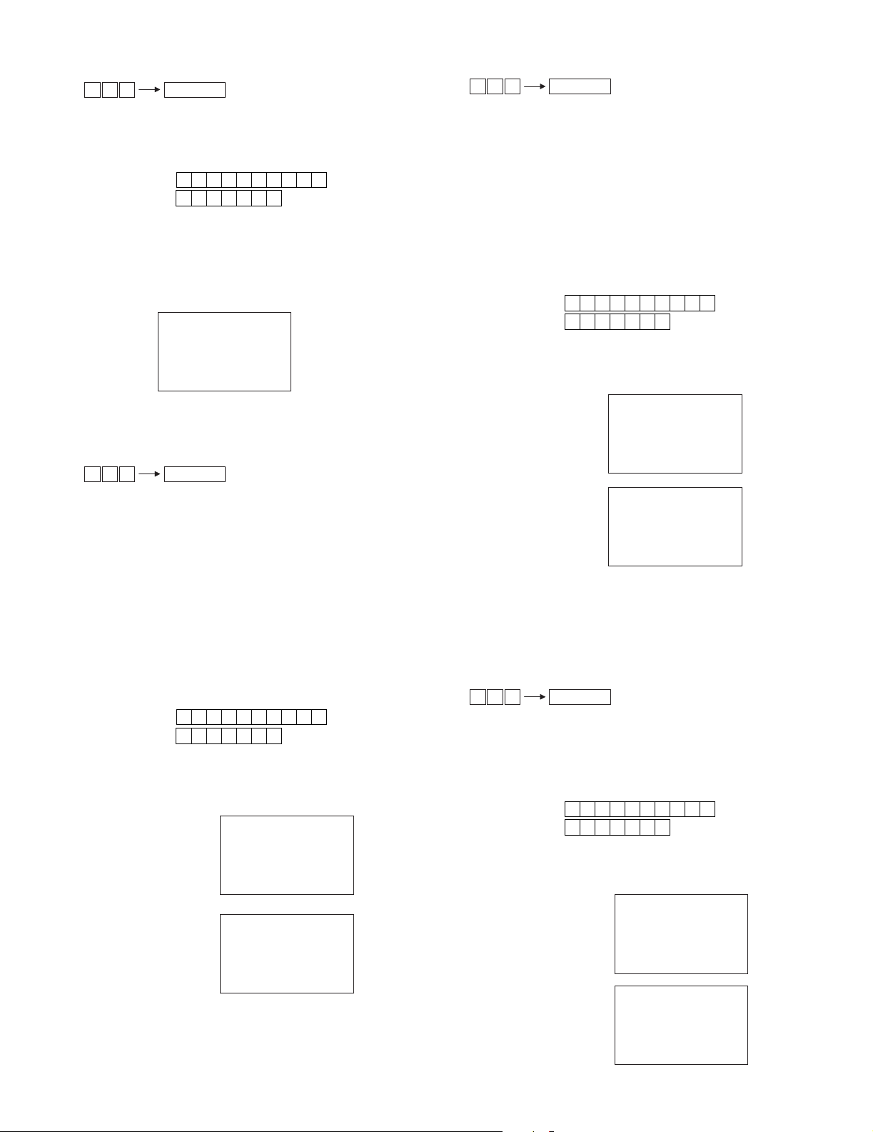
8) DRAWER OPEN TEST
1
Key operation
1 1 0
2
Test procedure
RCPT/PO
Drawer open.
3
Display
OP display:
1 1 0
POPUP display:
4
Check that
The drawer opens normally.
5
End of testing
The test will automatically be terminated and the printer prints as
follows.
End print:
110
9) EXTERNAL RAM TEST
1
Key operation
1 2 0
2
Test procedure
The standard 128 Kbyte RAM is checked.
The contents of the memory are lost after this test.
RAM (08000H ~ 27FFFH area) is tested in the following procedure.
a) Data in the test area is stored.
b) Write “00H”
c) Read and compare “00H” and then write “55H”
d) Read and compare “55H” and then write “AAH”
e) Read and compare “AAH”
f) Restore stored data.
3
Display
OP display:
POPUP display:
4
End of testing
The test will automatically be terminated and the printer prints as
follows.
When the
test ends normally:
When an error occurs:
RCPT/PO
1 2 0
RAM ERROR X *****h
120
120
10) CPU INTERNAL RAM TEST
1
Key operation
1 2 1
2
Test procedure
RCPT/PO
The test program checks internal RAM (24Kbyte) of the CPU.
The contents of the memory are lost after this test.
RAM (00400H - 053FFH area) is tested in the following procedure.
a) Data in the test area is stored.
b) Write “00H”
c) Read and compare “00H” and then write “55H”
d) Read and compare “55H” and then read “AAH”
e) Read and compare “AAH”
f) Stored data is restored.
3 Display
OP display:
1 2 1
POPUP display:
4
End of testing.
The test will automatically be terminated and the printer prints as
follows.
When the
test ends normally:
121
When an error occurs:
RAM ERROR X *****h
121
(*) x = 1: Data error x = 2: Address error
(*) When an error occurs, the printer outputs the error message
and then the address where the error has occurred in the
area “*****”.
11) CPU INTERNAL ROM TEST
1
Key operation
1 4 0
2 Test procedure
The test program checks that the checksum of the CPU internal
flash ROM (C0000H - FFFFFH) is correct.
The lower two digits of the checksum should be 10H.
3
Display
OP display:
POPUP display:
4
End of testing
The test will automatically be terminated and the printer prints as
follows.
When the
test ends normally:
RCPT/PO
1 4 0
ROM
140
********
********
(*) x = 1: Data error x = 2: Address error
(*) When an error occurs, the printer outputs the error message
and then the address where the error has occurred in the
area “*****”.
XE-A203U/XE-A203A TEST FUNCTION
– 13 –
When an error occurs:
RAM ERROR X *****h
ROM
********
********
120
Page 16
12) AD CONVERSION PORT TEST
1 Key operation
1 6 0
2 Test procedure
The AD value of each AD conversion port is sequentially displayed
for every 1 sec.
3 Display
OP display:
POPUP display:
(*)
X = 1: Head temperature X = 2: Head voltage X = 3: Battery voltage
(*) **** = A /D value
4
End of testing
When any key is pressed, the test is terminated and the AD value at
the terminating point is printed.
End print:
RCPT/PO
1 6 0 X
HEAD TEMP
HEAD VOLTAGE
BATTERY VOLTAGE
* * * *
160
***
***
***
15) SLEEP MODE TEST
1 Key operation
5 5 0
2 Test procedure
Check to confirm that the machine has entered the sleep mode
(display OFF, Dp ON), and wait for a change in status (key input,
change in RS port).
3 Display
OP display:
POPUP display:
4 End of the test
The test will automatically be terminated and the printer prints as
follows.
End print:
RCPT/PO
.
550
13) WINDING SPOOL CHECK TEST
1
Key operation
1 7 3
2
Test procedure
The winding spool motor is rotated for 2 sec.
3
Display
OP display:
POPUP display:
4 End of testing
The test will automatically be terminated and the printer prints as
follows.
End print:
14)
USB COMMUNICATION TEST (ID/ADDRESS PRINT)
1 Key operation
5 2 0
2 Test procedure
The USB revision, the vendor ID, the product ID, and the device
address assigned by the host are printed.
3 Display
OP display:
POPUP display:
4 End of the test
The test will automatically be terminated and the printer prints as
follows.
print:
RCPT/PO
1 7 3 .
173
RCPT/PO
5 2 0
USB Rev. Ver. XXX
VENDOR ID
PRODUCT ID XXX
DEVICE ADDRESS XXX
XXX
520
16) SD CARD TEST (SD CARD INFORMATION)
1 Key operation
6 2 0
2
Test procedure
The SD card is detected and the write protect status is displayed.
After completion of the test, the SD card register value is printed.
Error print list
SD CARD NO DETECT SD Card not detected
SD READ ERROR SD read error
3 Display
OP display:
POPUP display:
(*)
X = SD card detection
1 SD card YES
(*)
Y = WP detection
1 Write Protect state
4 End of the test
When any key is pressed, the SD card register is read and the end
print is made.
When the
test ends normally:
When an error occurs:
(*)
****** = Error print (Refer to the error print.)
RCPT/PO
Error print Error content
6 2 0 X-Y
X-Y
0 : SD card NO
0 :
Write Protect
620
XXXXXXXXXXXXXXXX
CID
XXXXXXXXXXXXXXXXh
CSD
XXXXXXXXXXXXXXXX
XXXXXXXXXXXXXXXXh
OCR
******
620
NO
12345678
--
--
h
XE-A203U/XE-A203A TEST FUNCTION
– 14 –
Page 17
B
B
B
D
D
D
D
C
C
C
C
B
A
1/4
12345678
12345678
12345678
12345678
f2
a2
e2
d2
dp 2
c2
g2
b2
f
b
e
a
d
c
g
dp
C5
0.1uF
VCC
2569121516
Q0Q1Q2Q3Q4Q5Q6
IC1
D0D1D2D3D4D5D6D7OC
347
D1
D0
D[0..7]
A[0..16]
D[0..7]
A[0..16]
VCC
1
2
3
4
5
6
7
8
9
RP3
10K
VCC
1
2
3
4
5
6
7
8
9
RP2
10K
VCC
R4
10K
R3
10K
R2
10K
R1
10K
A7
VCC:20pin
19
Q7
8
131417
18111
D2
D7
D5
D6D3D4
D3
A12
A9
A14
A11
A13
A8
A10
A1
A5
A6
A3D2A0
A2
A4
ENA12
VCC
GND:10pin
CLK
A15
A16
IN12
ENA22
R12
74HC374
VCC
IN22
KST32
/WR
NOT INSTALL
C9
33pF
10K
+
12
VDD
C7
C6
0.1uF
R22
10K
R21
10K
R23
10K
R24
10K
R5
10K
R28
10K
R27
10K
R26
10K
R25
10K
C4
C3
100pF*4(C10-C13)
C2
C1
KST02
KST22
KST12
/RD
R13
C12
33pF
10K
VCCVCC
A15
VDD
10uF/50V
C11
VCC
VCC
RP1
10K
A15
VCC
IC3
NC
A16
123456789
A16
R17
10k
VCC
/CS1
/CS2
/CS0
33pF
R16
10K
50494847464544434241403938373635343332
CS0
CS1
CS2
A19
51
A18
52
A17
53
A16
54
A15
55
A14
56
A13
57
A12
58
A11
59
A10
60
A9
61
VCC
62
A8
63
VSS
64
A7
65
A6
66
A5
67
A4
68
A3
69
A2
70
A1
71
A0
72
D15
73
D14
74
D13
75
D12
76
D11
77
D10
78
D9
79
D8
D6D5D4D3D2D1D0
D7
81808283848586878889909192939495969798
R44 33
R43 33
R41 33
R38
10K
R37
10K
1
2
3
4
5
6
7
8
9
D5
D7
D6
NOT INSTALL
A11
A8
A9
A13
A9
A8
WE
A13
CS2
A14
A12A7A6A5A4A3A2A1A0
A7
A3
A12
A4
A14
A5
A6
C8
33pF
/RD
/WR
TP1
RD
WR
CS3
BHE
HLDA
HOLD
CBCLK
IC2
FLASH M30626FHPFP 1006P6S-A
MASK M30624MWP-XXXFP
AN7
AN6
R48 33
R47 33
R46 33
R45 33
R49 33
/LAT2
/STB12
D0
D4
D1
D3
VDD
R14
D5
D7
A10
D6
A10OEA11
I/O5
I/O6
I/O7
CS1
I/O0
I/O1
10111213141516 17
A1
D0
D1
A2
SD_RXD 4
DR1 2
SD_CLK 4
SD_RXD
SD_CLK
ALE
CLK0
RTS0
RXD0
CLKOUT
AN5
AN4
AN3
AN2
AN1
P1012
VBAT3
/STB22
VPON3
/CS2
NOT INSTALL
CN2
Not Install
VCCVCC
IC6
VCC
R39
10K
VCC
R51
TB5OUT
30
TB5IN
29
TA1OUT/V
28
TA1IN/V
27
TA2OUTW
26
TA2INW
25
TBEOUT
24
TB3IN
23
TA4OUT/U
22
TA4IN/U
21
INT0
20
INT1
19
INT2
18
NMI
17
VCC
16
XIN
15
VSS
14
XOUT
13
RESET
12
XCOUT
11
XCIN
10
CNVSS
9
BYTE
8
CLK3
7
SIN3
6
SOUT3
5
TB3IN
4
TB4IN
3
CLK4
2
SOUT4
1
VDD
4.7UF/50V
2
C19
Not Install
R42
R15
47K
R53
123456789
VCC3
VCC
0.1uF
BD3
BD1
BD2
BD0
18171615141312
B0B1B2B3B4B5B6
A0A1A2A3A4A5A6A7G
2345678
D2
D0
D3
D1
R50
DAT 2
10K
R42 XE-A20W ONLY
10K
100K
CN3
TEST PIN
VCC
CNVss
ONLY QA0/QA1 USE
33pF
C18
10K
D4
D3
181920212223242526272829303132
I/O4
I/O2
VSS I/O3
LP621024DM-70MM/ CY62128BLL-70SXC SOIC
D2
/SD_CD 4
/SD_POW 4
/SD_CS 4
/SD_WP 4
SD_TXD 4
/SD_CS
SD_TXD
/SD_WP
/SD_POWER
/SD_CD
31
CLK1
TXD0
TXD1
RXD1
CLKS1
AVSS
AN0
VREF
AVCC
SIN4
99
100
VDD
P1002
P972
C10
+
1
VCC
BD[0..7]
BD5
BD4
D4
10K
P962
C13
RXDPRG
TXDPRG
R64 0
R65 0
/SD_WP
/SD_CD
1011121314151617181920212223242526
BD6
BD1
BD5
BD3
BD7
BD4
BD0
BD2
BD7
BD6
74ALS645
11
B7
DIR
IC7
9191
D7
D6
/CS1
/RD
R52
10K
BZ1
+
B
CLK 2
PIEZO BZ
R40
10K
D1
1SS133
1 2
1K
/POFF 3
MOTOR 2
R58
/RESUSB
R61
R62
P952
P912
P942
P932
P902
P922
IC4
1000pF
Reset IC
12345
VDD
R56
3.3K
BA1
BA3
BA4
/CS1B
BA2
BA6
BA5A0/RD_B
BA0
23222120191817
2345678
R40 XE-A203U/A ONLY
/DREQUSB
/WR_B
16
15
14
A1D5A0
A2
A3
A4
A5
123456789
VCC3
VCC
3
1
/INTUSB
X2
330
R60
47K
CNVss
4
NC
SII
VDD
VSS
rohm
BD5228/ S80928
231 5
C14
100pF
820
/RESET2
54
9131
A6
/CS1
VDD
D0
D1
X3
1 2
C15
Y9
Y8
10
11
/WR
/RD
12
D2
C24
C21
C20
2200pF
Y10
C17
+
D4
0.1uF
27pF
18pF
132
Y1Y2Y3Y4Y5Y6Y7
A1A2A3A4A5A6A7A8OE2
0
OUT CD
R57
1.0-11-26P
74ABT827
OE1A9A10
/RESUSB_B
/DREQUSB
/INTUSB
0.1uF
C16
10uF/50V,AL
1011121314151617181920212223242526
A0
A6
D7
D5
A2
A3
A5
A4
D6
2
CSTLF12M
32.768KHz
X1
BD5228
A1
VCC
VCC
IC5
3
VDD
XIN
123
2
R20
R19
R18
Not Install
12
C22
678
S0
FSOUT
XOUTS1LF VSS
1
C23
4 5
/CS1
10K
10K
10K
+
0.1uF
FS781
R63
/RD
/WR
/DREQUSB
10uF/10V,OS
3.3K
C25
CST12.0MTW
/RESUSB_B
/INTUSB
R66
330pF
21
21
21
21
3
3
3
3
CN1
52806-2610
TO USB
C27
1000pF
R70 0
C26
91pF
33
CPU CIRCUIT
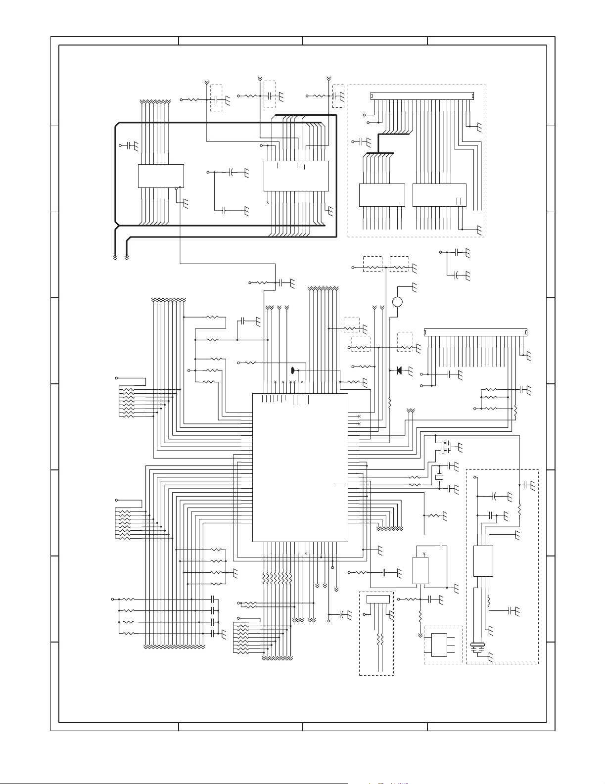
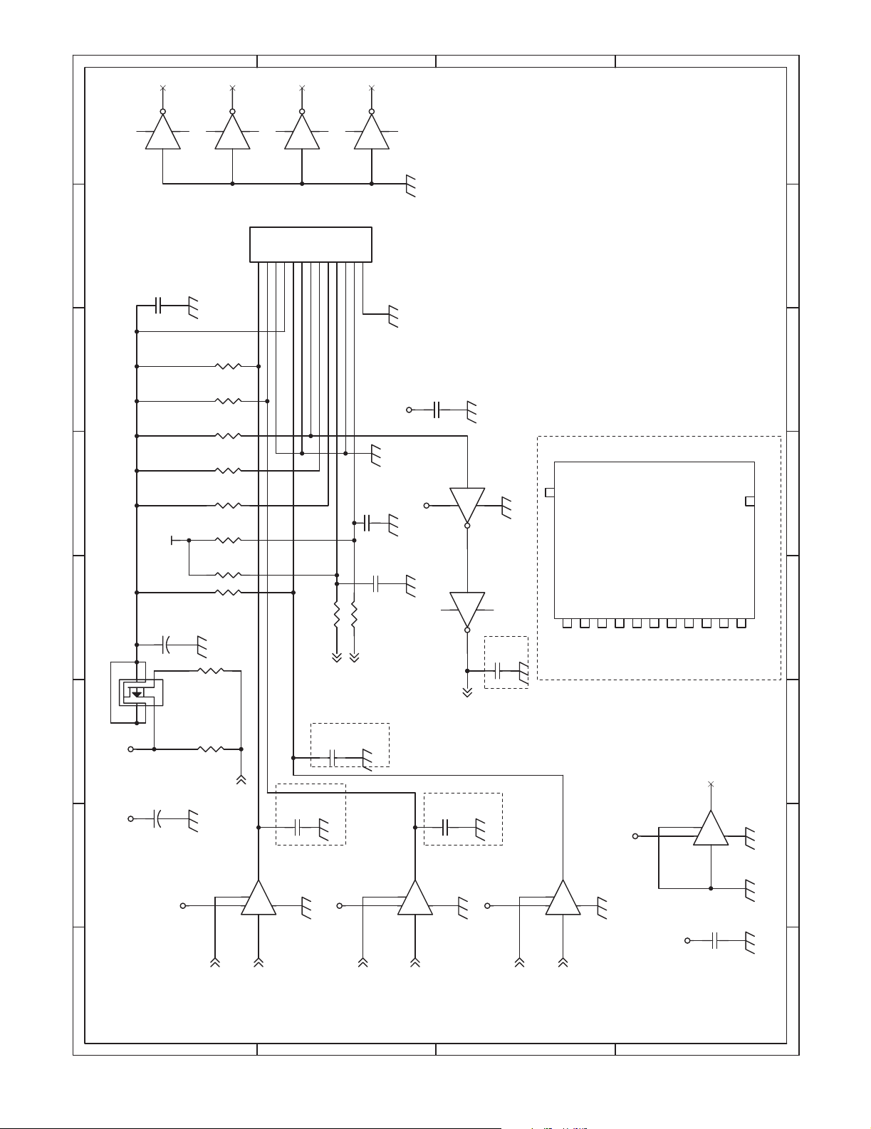
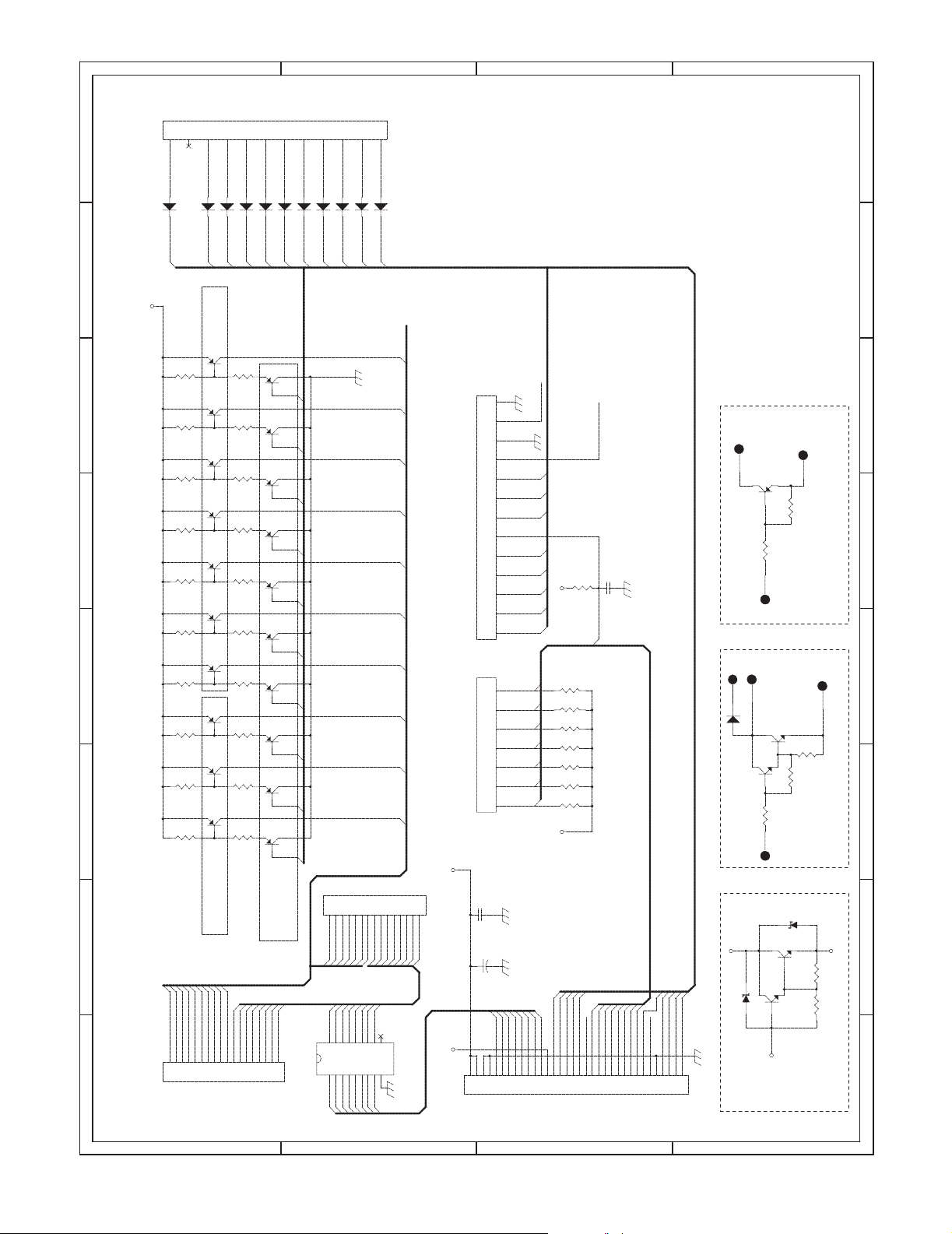
CHAPTER 6. CIRCUIT DIAGRAM AND PWB LAYOUT
■ MAIN PWB
87654
87654
87654
87654
B
B
B
D
D
D
D
C
C
C
C
B
A A
A A
A A
A
XE-A203U/XE-A203A CIRCUIT DIAGRAM AND PWB LAYOUT
– 15 –
Page 18
B
B
B
D
D
D
D
C
C
C
C
B
A
2/4DRIVING CIRCUIT
12345678
12345678
12345678
12345678
VP
VO 2,3
84
CN4
NOT INSTALL
7
+
-
5
6
MOTOR
1
2
EH-2A
C28
0.1uF
IC8B
BA10393
3
C
DRAWER
123
CN5
Q1
2SD2212
3 2
1
1K
R76
MOTOR1
TP2
2510-3A
STRAIGHT CON
FB2
D18
1N4002
C34
0.1uF
FB1
C66673
JUMPER WIRE(FB1)
VDR
F1
T500mA/250V
VO
C66673
1 2
JUMPER WIRE(FB2)
Q4
2SD2212
2
3
1
1.8K
R77
+
C35
10uF/50V
DR11
3
D
1SS133
D4
1 2
1
EB
2
KRC111S
12
SG
2SK2731
VP
4113512
VS1
VS2
IC11
VCC
ENA1
1
213697
VCC
ENA11
AS
/AS
OUT1
ENA2
ENA2
1
BS
OUT2
OUT3
IN1
IN11
/BS
10
OUT4
IN2
IN2
1
E
2
13
2SD2212
BC
C39
10uF/50V
+
1
2
8
VCONT
LB1838M
GND
GND
14
21
21
21
21
3
3
3
3
VCC
C31
3
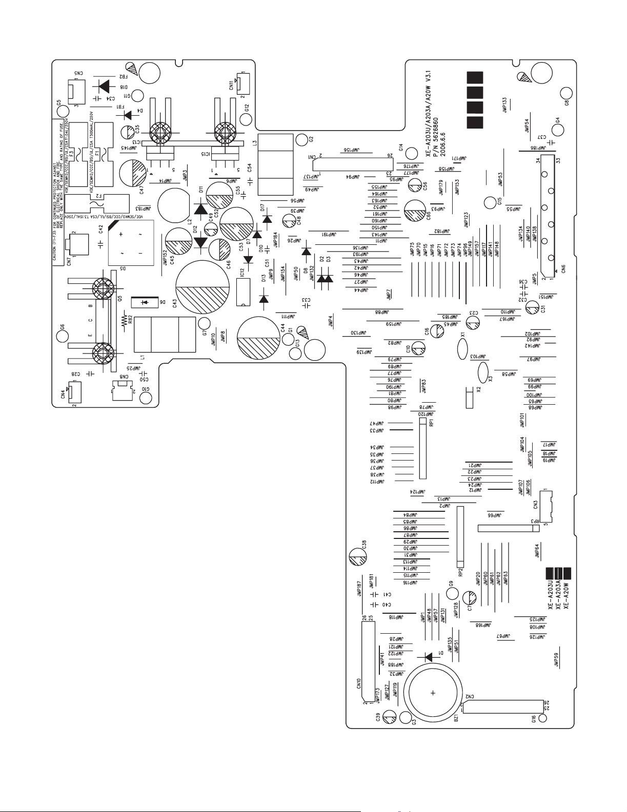
R71
56KF
TCOFF
1
84
+
3
2
R73
30KF
VCC
R72
10KF
IC8A
BA10393
-
R75
5.1KF
P100 1
C30
330pF
TH1
C29
0.1uF
R74
10KF
P1011
VCC
VO 1,3
VP
VCC
VCC
IC9
ABC
1234567
KST01
S
1
D2
2
/S4
+
12
C32
/S2
/S0
/S1
Y0
KST31
KST21
KST11
PE
2
G
1SS133
10uF/50V
0.1uF
/S3
/S4
G2BG1Y7
G2A
C33
3 1
D
P91
P911
/S5
10111213141516
/S7
0.1uF
Q2
/S6
Y5Y4Y3Y2Y1
GND Y6
8 9
2SK2731
74HC138
VCC
/S8
/S9
Y0
VCC
IC10
ABC
1234567
HUPS
2
Q3
P911
C36
G2A
D3
0.1uF
G2BG1Y7
KRC111S
1 3
1
2
/S3
10111213141516
Y5Y4Y3Y2Y1
GND Y6
8 9
1SS133
74HC138
VLED
VCCVP
VCC
CN6
TH 1
/LAT 1
/BSASBS
/AS
R10
10K
C38
47uF
50V
+
12
12345678910111213141516171819202122232425
CN10
C37
0.1uF
f1
c1
b1
d1
a1
d
a
b
c
dp 1
e1
g1
dp
e
f
g
/S1
/S7
/S0
/S2
/S0
/S1
/S2
/S7
/S8
/S8
/RESET
HUPS
C41
CLK 1
/STB1 1
/STB2 1
DAT 1
PE
0.1uF
R81
4.7K
C40
0.1uF
2K
R80
R11
10K
26
1.0-11-26P
PRINTER CN
P95 1
/S9
P90 1
/RESET 1
P91 1
P93 1
P92 1
P93
P94
P91
P90
P92
/S3
P96 1
P94 1
P97 1
P95
P96
P97
10111213141516171819202122232425262728293031323334
/S6
/S5
/VON 3
/S4
/S3
/S4
/S5
/S9
/S6
/VON
123456789
1.25-2-34P
87654
87654
87654
87654
KEY CN
B
B
B
D
D
D
D
C
C
C
C
B
A A
A A
A A
A
XE-A203U/XE-A203A CIRCUIT DIAGRAM AND PWB LAYOUT
– 16 –
Page 19

B
B
B
D
D
D
D
C
C
C
C
B
A
3/4POWER CIRCUIT
C
12345678
12345678
12345678
12345678
3
C
3
Q1:HEAT SINK
F2
1
KRA106S
BE
2
KRC106S
21
BE
VP
L1
63uH
IPEAK>12A :100%
with FUSE
32
Q5
KTD998
1
D5
4
-+
3
C42
MYLAR
0.033uF
3.15A
1
2
CN7
D
D
D
D
3
2
BEC
KTD998
1
ZD1
PTZ9.1B
1 2
+
12
C44
16V
4700uF
R83
17.8KF
R85
3.3KF
D6
FMB-G24H
12
R86
18K
R82
10(FUSE)
1
L:ON
6,8pin:N.C
LM2574
1
3
2
4
IC12
5 7
R84
22K
50V
3300uF
+
12
C43
2
BR32
VH-2A
FROM TRANSFORMER
H:OFF
VBAT 1
R94
22K
VDD
VCC
D13
RB721Q
VCC +5V
VCC +5V
VLED +5.8V
2
D11
1
VLED
L2
180uH
12
D9
RB060L40
2
Q6
KRC106S
0
R88
24K
R87
1 3
2
D7
1SS133
1 2
1
R89
2.2K
D8
2
TCOFF2
VPON1
/POFF1
VO 1
C
C
C
C
1SS133
PQ1CG2032FZ
4
IC13
HEAT SINK
1
1SS133
D10
2
F3
/VOFF
VOUT
VIN
1
ADJ
VLED
VCC
1N4002
1.0A
2
1N4002
D12
1
C45
+
12
R92
5
ON/OFF
COM
R91
9.1KF
R90
2.7K
C46
+
12
ZD2
16V
1000uF
2.7KF
D14
3
12
R93
2.7K
NOT
R99
R97
1 2
330uF
PTZ6.2B
12
R96
RB060L40
+
C47
R95
1
C48
INSTALL
CN8
100
R100
220
16V
1 2
C49
+
910F
1 2
220uF/50V
8
56K
8
R98
0
+
1uF/50V
1
2
3.3M
0.1uF(M)
C50
10uF/10V OS
/POFF 1
7
+
-
5
6
1
+
-
3
2
2
NOT
IC14A
TJC3-2A(BLUE)
FROM BATTERY
INSTALL
/VOFF
/VOFF
L:OFF
H,OPEN:ON
PQ1CG2032FZ
4
12
B
B
B
B
0.1uF
RB060L40
HEAT SINK
IC15
D15
4
IC14B
BA10393
BA10393
4
R101
C51
3.9KF
VO 1
VO:23.8V
12
VO
R7
10K
L3
220uH
2
VOUT
ADJ
VIN
1
12
R6
P-OFF
ZD3
UDZS5.1B
C53
D16
5
10K
1 2
+
ON/OFF
COM
+
C52
1000uF/35V
R105
560
RB060L40
1 2
3
220uF/50V
10K
R8
21
21
21
21
3
3
3
3
C54
0.022uF(M)
R9
10K
Q8
KRC106S
1 3
2
12
ZD5
UDZS4.3B
D17
1SS133
1 2
Q7
KRA106S
13
2
R107
33
/VON2
NOT
INSTALL
ZD4
UDZS5.1B
1
2
0.1uF
C55
87654
87654
87654
87654
A A
A A
A A
A
XE-A203U/XE-A203A CIRCUIT DIAGRAM AND PWB LAYOUT
– 17 –
Page 20
B
B
B
D
D
D
D
C
C
C
C
B
A
1 2
C57
1uF
VCC
C56
1uF/50V
+
12
6
4
213
Q9
74HCT04
HAT1089C
4/4SD CARD CIRCUIT
12345678
12345678
12345678
12345678
IC16A
147
G:6pin
D:2,3,4,5pin
S:1pin
5
VCC3
IC16B
147
3 4
CN9
R117
100K
R116
100K
R115
100K
R114
100K
R113
100K
R112
10K
R111
10K
100K
R104
51
R110
R109
10K
74HCT04
IC16C
147
5 6
CSDIVSS
VDD
SCLK
VSS2DORSV
123456789
74HCT04
IC16D
147
RSVCDSWWPGND
101112
R119 33
R118 33
/SD_WP1
/SD_CD1
C59
100pF
9 8
13
C65
1000pF
C64
1000pF
NOT INSTALL
74HCT04
ALPS SCDA2A0300
C63
0.1uF
VCC
14Pin : VCC
7Pin : GND
147
VCC
IC16F
147
IC16E
21
21
21
21
3
3
3
3
1312
74HCT04
1110
74HCT04
C62
100pF
SD_RXD1
WP
#12
COMMON
SD Card Pin Layout
#7
NOT INSTALL
#11
#8
#5
#6
GND
#13
CD
#9
#2
#4
#3
#10
#1
12
VCC3
C66
100uF/50V
+
VCC3
14Pin : VCC3
7Pin : GND
D
D
D
D
IC17A
W
/SD_PO
1
IC17C
C60
C58
100pF
/SD_POW1
1
14
74LV125
7
2 3
/SD_CS1
NOT INSTALL
IC17B
4
VCC3
XE-A203U/XE-A203A CIRCUIT DIAGRAM AND PWB LAYOUT
14
/SD_POW1
C
C
C
C
100pF
NOT INSTALL
IC17D
74LV125
7
5 6
SD_TXD1
VCC3
13
14
/SD_POW1
B
B
B
B
74LV125
12 11
SD_CLK1
VCC3
7
10
14
VCC3
C61
74LV125
7
9 8
0.1uF
87654
87654
87654
87654
A A
A A
A A
A
– 18 –
Page 21
B
B
B
D
D
D
D
1/1
12345678
12345678
12345678
12345678
CN1
10
11
12
7
8
9
4
5
6
C
C
C
C
1
2
3
52045-1245
B
A
VLED
12
12
1SS133
1SS133
D30
D20
/S0
/S1
KTA1663 * 7
Q20
3
1
12K
R138
Q19
32
1
12K
R137
Q18
32
1
12K
R136
Q17
32
1
12K
R135
Q16
32
1
12K
R134
Q15
32
1
12K
R133
Q14
32
1
12K
R132
Q13
32
1
12K
R131
Q12
32
1
12K
R130
Q11
32
1
12K
R129
KTA1664 * 3
12
12
12
D24
/S4
/S0
/S1
/S2
/S3
/S4
/S5
/S6
/S7
/S8
/S9
or DTA143ESA
1SS133
1SS133
D25
D26
/S5dp/S7
/S[0..9]
CN13
12
1SS133
D27
/S6
G1
G2
G3
G4
G6
G7
G8
G9
G10
52806-1510
G2
G1
12
12
12
1SS133
1SS133
1SS133
D28
G4
G3
G5
G6 /S8
FROMKEY
D29
/S9
21
21
21
21
G[1..10]
13
/VON
12
11
10
9
/S0
8
/S1
7
/S2
6
MDR
P:2.0mm HOLE ONLY
5
CON3
C72
C71
+
4
3
2
1
7
6
5
4
3
2
1
0.1uF
100uF/16V
/S3
/S4
/S5
/S6
/S7
P97
P96
P95
P94
P93
P92
P91
FROM MODE SWITCH
52045-0745
FROM KEY
CN15
VLEDVCC
123456789101112131415
e
b
f
c
dp
d
a
G7
VLED
FOR POP UP
12
/RESET
OUTPUT
47K
C73
R128
VCC
100pF
COMMON
47K
4.7K
INPUT
P90
R127
47K
R126
47K
R125
47K
R124
47K
R123
47K
R122
47K
R121
47K
VCC
P[90..97]
OUT P UT
COMMON
INPUT
3K
7.2K
2.7K
C
3
3
3
3
KRA101M, KRA106S
GND
KID65083
E
12
12
1SS133
1SS133
1SS133
D23
D21
D22
/S2
/S1
/S3
2
Q30
12
120
3
R148
Q29
12
120
3
R147
Q28
12
120
3
R146
Q27
12
120
3
R145
Q26
12
120
3
R144
Q25
12
120
3
R143
Q24
12
120
3
R142
Q23
12
120
3
R141
Q22
12
120
3
R140
Q21
12
120
3
R139
KRA101M * 10
d
e
G1
G7
G8
G9
G10
c
G3
G5G5G4
G2
G6
b
a
978654321
FOR MAIN DISPLAY KEY
■ KEY IF CIRCUIT
D
D
D
D
g
f
181716151413121110
P:2.0mm HOLE ONLY
CON2
d
f
c
b
a
g
181716151413121110
181716151413121110
123456789
IC18
123456789
G1
DP1
F1dpC1
E1
KID65083AP(DIP)
A1
B1eD1
C
C
C
C
CN12
52045-3445
A1gD1
XE-A203U/XE-A203A CIRCUIT DIAGRAM AND PWB LAYOUT
– 19 –
3.5K 300
1
F1
DP
E1
C1
B1
G1
/RESET
/S0
P91
P90
/S1
P93
/S7
/S2
P92
/S8
P94
/S4
P95
P96
/S6
P97
/VON
/S5
/S3
/S9
B
10111213141516171819202122232425262728293031323334
B
B
B
B
123456789
FROM MAIN BOARD
87654
87654
87654
87654
2SD2170
A A
A A
A A
A
Page 22
B
B
B
23
35
22
34
21
33
20
32
31
30
29
16 195328
15 18
27
14 17
26
13
12
24 25
B
47
59
46
58
57
4540
56
4439
55
4338
54
42
41
52
51
50
3736
48 49
D
D
D
D
1/1
12345678
12345678
12345678
12345678
C
C
C
C
11
10
9
8
7
6
5
4
3
2
1
¡ü
A
21
21
21
21
3
3
3
3
48
36
49
37
5038
5152
54
53
55
43
56
44
57
45
58
59
47
FOR KEY I/F BOARD
P97
13
1
12
24
¡ü
14
2
26
25
15
3
27
39
17
5
29
40 28 164
41
18
6
30
42
19
7
31
32
8
21 20
33
10
9
22
34 46
11
23
35
P96
P95
P94
P93
P92
P91
7
6
5
4
3
2
1
1.25mm FPC CN
CN2
/S1
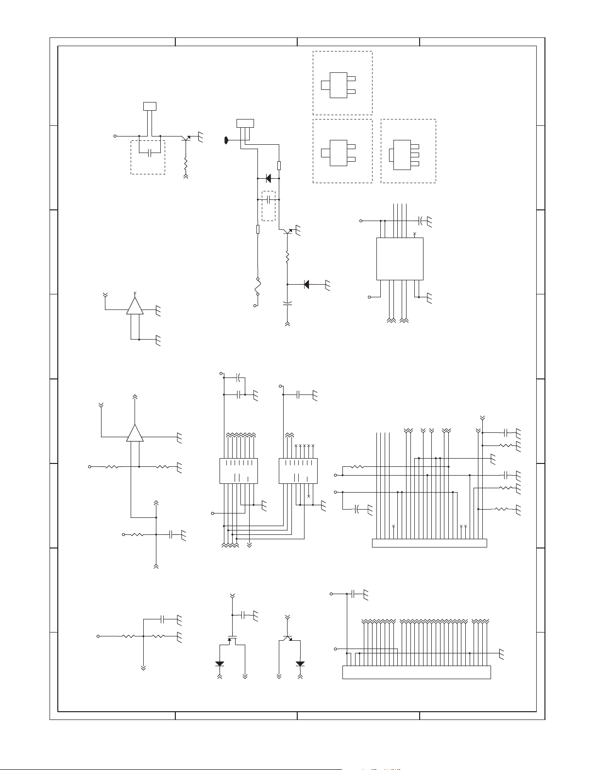
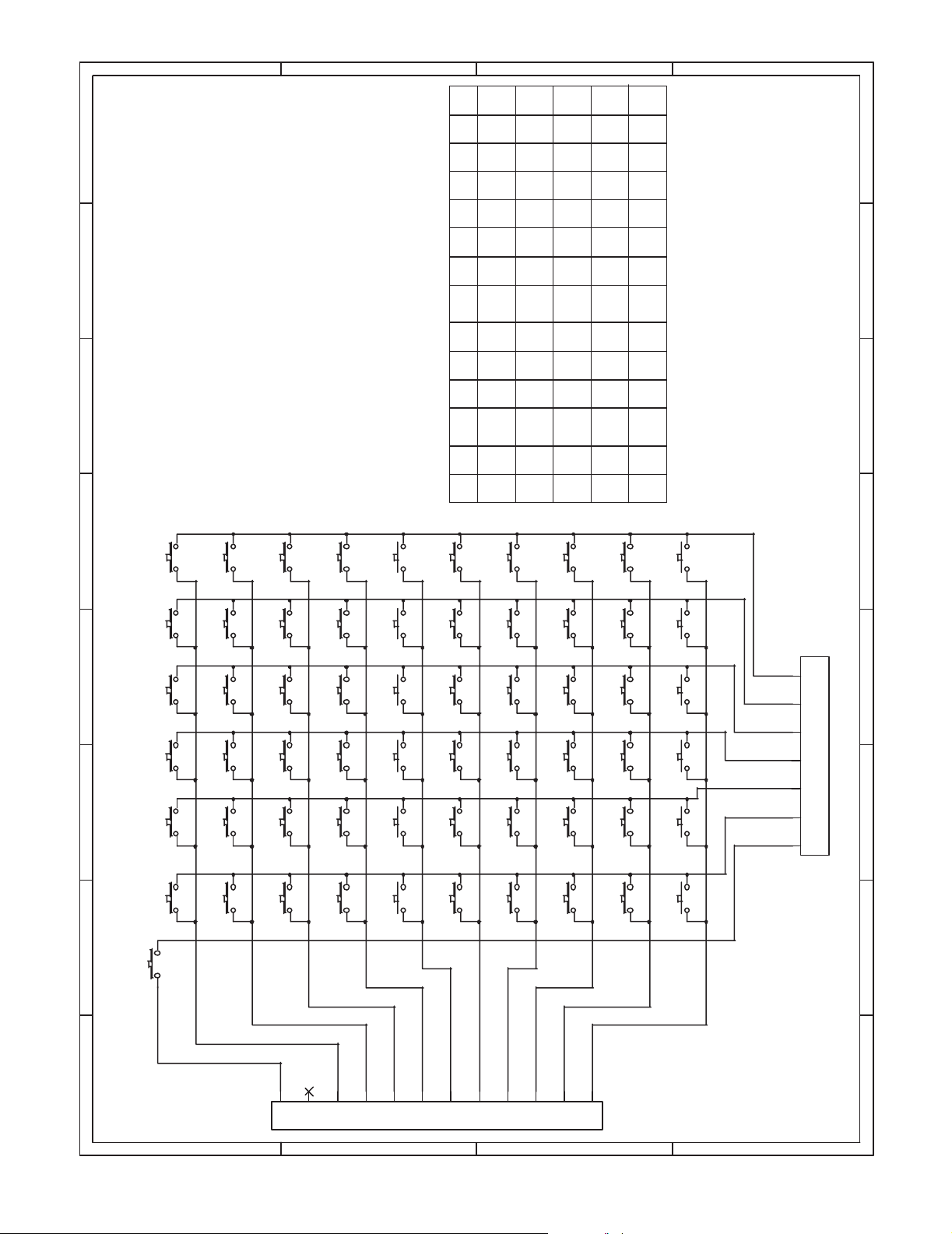
■ KEY-MTX CIRCUIT
D
D
D
D
CN1
87654
87654
87654
/S0
/S1
1
2
3
4
XE-A203U/XE-A203A CIRCUIT DIAGRAM AND PWB LAYOUT
C
C
C
C
/S2
/S3
/S4
/S5
5
6
7
– 20 –
/S7
/S8
11
/S9
12
B
B
B
B
1.25mm FPC CN
FOR KEY I/F BOARD
A A
A A
A A
A
/S6
8
9
10
87654
Page 23

B
B
B
D
D
D
D
C
C
C
C
B
A
1/1
12345678
12345678
12345678
12345678
1312
LED5
LA56S2-S2
1312
G4G7G10
LED6
LA56S2-S2
G5G8 G1
1312
G6
LED7
DISPLAY PWB
LA56S2-S2
11
aabbccdd
10
8
6
e
5
7
gg
9
dpdp
16
15 14
3
2
1
eff
18
17
4
21
21
21
21
11
aabbccdd
10
8
6
5
e
7
gg
9
dpdp
16
15 14
3
2
1
eff
18
17
4
11
10
8
6
5
f
7
gg
9
16
15 14
3
2
1
f
18
17
4
dp dp aabbccddee
3
3
3
3
1312
LED8
LA56S2-S2
G9 G3
1312
LED9
LA56S2-S2
G[1..10]
11
aabbccddeeffggdpdp
10
8
6
5
7
9
16
15 14
3
2
1
18
17
4
aabbccddeeffggdpdp
11
10
8
6
5
7
9
16
15 14
3
2
1
18
17
4
G7
G2G2G6
G1
G10
G9
G4
G8
G3
30 1/6WR33
R29 30 1/6W
R30 30 1/6W
R32 30 1/6W
R31 30 1/6W
R35 30 1/6W
R34 30 1/6W
R36 30 1/6W
G5
87654
87654
87654
87654
■ MAIN DISPLAY CIRCUIT
D
D
D
D
CON1
B
B
B
C
C
C
C
B
XE-A203U/XE-A203A CIRCUIT DIAGRAM AND PWB LAYOUT
– 21 –
978654321
181716151413121110
HOLE ONLY
A A
A A
A A
A
Page 24
B
B
B
D
D
D
D
1/1
12345678
12345678
12345678
12345678
C
C
C
C
B
13
A
21
21
21
21
GND
/VON
0
000
00
MODE SWITCH
SW1
GND
1
2
3
4
5
6
7
8
9
10
/RE-
/S0/S1/S2MOR/S3/S4/S5/S6/S7
SET
12
11
10
9
8
7
6
5
4
3
2
1
FOR KEY I/F BOARD
CN1
P:2.0mm HOLE ONLY
3
3
3
3
■ MODE SWITCH CIRCUIT
D
D
D
D
B
B
B
C
C
C
C
XE-A203U/XE-A203A CIRCUIT DIAGRAM AND PWB LAYOUT
– 22 –
B
87654
87654
87654
87654
A A
A A
A A
A
Page 25

B
B
B
D
D
D
D
1/1
12345678
12345678
12345678
12345678
C
C
C
C
123456789101112131415
CN1
G2'
G3'
G1'
A'
G4'
G7'
G5'
G6'
B'
B
52807-1510
F'
C'
G'
DP'
D'
E'
FROM KEY I / F BOARD
a
11
11
bcdefdpabcdef
10
10
8
86579
12
16
15
321
18
174
11
10
86579
12
16
15
321
18
174
11
10
86579
12
16
15
321
18
174
510912467
6
5
12
g
7
9
16
15
3
2
1
18
gdp
17
4
a
11
bcdefdpabcdef
10
8
6
5
12
g
7
9
16
15
3
2
1
18
gdp
17
4
a
11
bcdefdpabcdef
10
8
6
5
12
g
7
9
16
15
3
2
1
18
gdp
17
4
7
abcdef
6
4
2
1
9
10
gdp
5
R1
R2
27 1/6W
R3
27 1/6W
R4
27 1/6W
R5
27 1/6W
R6
27 1/6W
A'G'
27 1/6W
B'
C'
D'
E'
F'
13
13
LED1
LA56S2-S2
14
14
13
13
LED2
LA56S2-S2
LED3
LA56S2-S2
LED4
LA56S1-S2
14
14
13
13
14
14
8
,
38
3
G4' G3' G2' G1'
G5'
G6'
G7'
A
21
21
21
21
3
3
3
3
■ POPUP CIRCUIT
D
D
D
D
B
B
B
C
C
C
C
XE-A203U/XE-A203A CIRCUIT DIAGRAM AND PWB LAYOUT
B
– 23 –
R7
27 1/6W
87654
87654
87654
DP'
R8
27 1/6W
A A
A A
A A
A
87654
Page 26

B
B
B
D
D
D
D
1/1
12345678
12345678
12345678
12345678
19
20
21
22
23
24
25
26
27
C
C
C
C
10
11
12
13
14
15
16
17
18
B
CN2
52806-2710
TO PRI NTER
123456789
A
21
21
21
21
5VVP
/B
/A
A
B
VP
TH
LAT#
GND
GND
5V
STB1#
STB2#
GNDVPCLK
GND
DAT
VP
VP
5V
PE
LEDK
HUPS
VP 5V
C2
C1
01.uF NOT MOUNT
0.1uF NOT MOUNT
3
3
3
3
12345678910111213141516171819202122232425
■ PRINTER I/F CIRCUIT
D
D
D
D
26
CN1
52806-2610
B
B
B
C
C
C
C
XE-A203U/XE-A203A CIRCUIT DIAGRAM AND PWB LAYOUT
B
– 24 –
TO MAI N PWB
BE CAREFUL FOR DI RECTI ON OF
CONNE CTER!
87654
87654
87654
87654
A A
A A
A A
A
Page 27
PWB LAYOUT
1. MAIN PWB LAYOUT
Top side
XE-A203U/XE-A203A CIRCUIT DIAGRAM AND PWB LAYOUT
– 25 –
Page 28

Bottom side
XE-A203U/XE-A203A CIRCUIT DIAGRAM AND PWB LAYOUT
– 26 –
Page 29

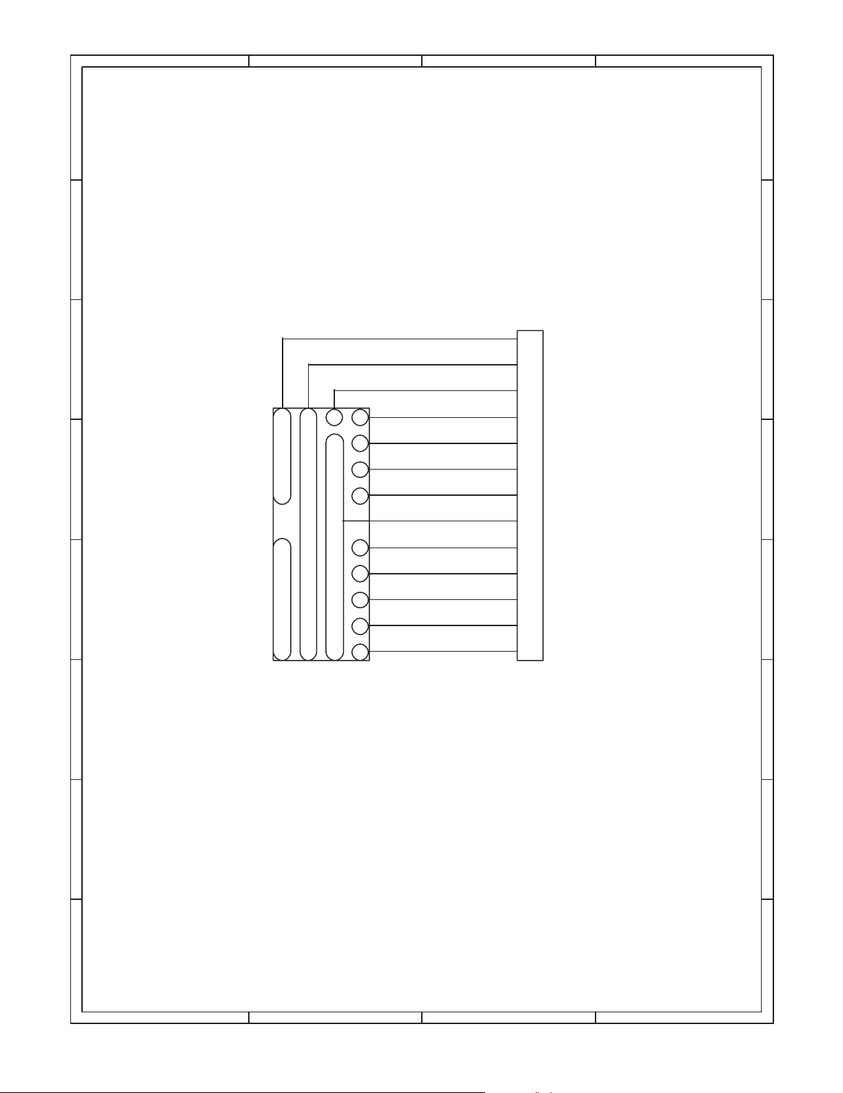
2. KEY INTERFACE PWB LAYOUT
Top side
Bottom side
XE-A203U/XE-A203A CIRCUIT DIAGRAM AND PWB LAYOUT
– 27 –
Page 30

3. PRINTER I/F PWB LAYOUT
Top side
Bottom side
4. REAR DISPLAY PWB LAYOUT
5. DISPLAY PWB LAYOUT
XE-A203U/XE-A203A CIRCUIT DIAGRAM AND PWB LAYOUT
– 28 –
Page 31

q
COPYRIGHT
No part of this publication may be reproduced,
electronic, mechanical, photocopying, recording, or otherwise,
without prior written permission of the publisher.
2006 BY SHARP CORPORATION
All rights reserved.
Printed in Japan.
stored in a retrieval system, or transmitted.
In any form or by any means,
SHARP CORPORATION
Information and Communication Systems Group
Quality Assurance Department
Yamatokoriyama, Nara 639-1186, Japan
2006 July Printed in Japan t
 Loading...