

SGS Thomson Microelectronics ST72F652R4T1, ST72F652, ST72F651R6T1, ST72F651AR6T1, ST72F651 Datasheet
...
June 2003 1/166
This is preliminary information on a new product. Details are subject to change without notice.
Rev. 2.3
ST7265x
LOW-POWER, FULL-SPEED USB 8-BIT MCU WITH 32K
FLASH, 5K RAM, FLASH CARD I/F, TIMER, PWM, ADC,
I2C, SPI
DATASHEET
■ Memorie s
– Up to 32K of ROM or High Density Flash (HD-
Flash) program memory wi th read/ write protect ion
– For HDFlash devices, In-Application Pro-
gramming (IAP) via USB and In-Circuit programming (ICP)
– Up to 5 Kbytes of RAM with up to 256 bytes
stack
■ Clock, Re set and Supply Manag e m ent
– PLL for generating 48 MHz USB clock using a
12 MHz crystal
– Low Voltage Reset (except on E suffix devic-
es)
– Dual supply management: analog voltage de-
tector on the USB power line to enabl e s ma rt
power switching from USB power to battery
(on E suffix devices).
– Programmable Internal Voltage Regul ator for
Memory cards (2.8V to 3.5V) supplying:
Flash Card I/O lines (voltage shifting)
Up to 50 mA for Flash card supply
– Clock-out capability
■ 47 pro grammable I/O li ne s
– 15 high sink I/Os (8mA @0.6V / 20mA@1.3V)
– 5 true open drain outputs
– 24 lines programmable as interrupt inputs
■ USB (Universal Serial Bus) Interface
– with DMA for full speed bulk applications com-
pliant with USB 12 Mbs spec ification (version
2.0 compliant)
– On-Chip 3.3V USB voltage regulator and
transceivers with software power-down
– 5 USB endpoints:
1 control endpoint
2 IN endpoints supporting interrupt and bulk
2 OUT endpoints supporting interrupt and
bulk
– Hardware conversion between USB bulk
packets and 512-byte blocks
■ Mass Storage Interface
– DTC (Data Transfer Coprocessor): Universal
Serial/Parallel communications in terface, with
software plug-ins for current and f uture prot ocol standards:
Compact Flash - Multimedia Card -
Secure Digital Card - SmartMediaCard Sony Memory Stick - NAND Flash ATA Peripherals
■ 2 Timers
– Configurabl e Watchdog for syst em reli ability
– 16-bit Timer with 2 output compare functions.
■ 2 Communication Interfaces
– SPI synchronous serial interface
–I
2
C Single Master Interface up to 400 KHz
■ D/A and A/D Peripherals
– PWM/BRM Generator (with 2 10-bit PWM/
BRM outputs)
– 8-bit A/D Converter (ADC) with 8 channels
■ Instruction Set
– 8-bit data manipulation
– 63 basic instructions
– 17 main addressing modes
– 8 x 8 unsigned multiply instruction
– True bit manipulation
■ Development Tools
– Full hardware/software development package
Device Summary
TQFP64 10x10
TQFP48
SO34 shrink
Features ST72651 ST72F651 ST72652
Program memory 32K ROM 32K FLASH 16K ROM
User RAM (stack) - bytes 5K (256) 512 (256)
Peripherals USB, DTC, Timer, ADC, SPI, I
2
C, PWM, WDT USB, DTC, WDT
Operating Supply
Dual 2.7V to 5.5V or
4.0V to 5.5V (for USB)
Dual 3.0V to 5.5V or
4.0V to 5.5V (for USB)
Single 4.0V to 5.5V
Package TQFP64 (10 x10) TQFP64 (10 x10) / TQFP48 (7x7) / SO34
Operating Temperature 0°C to +70°C
1

Table of Cont ents
2/166
-
1 INTRODUCTION . . . . . . . . . . . . . . . . . . . . . . . . . . . . . . . . . . . . . . . . . . . . . . . . . . . . . . . . . . . . . . 4
2 PIN DESCRIPTION . . . . . . . . . . . . . . . . . . . . . . . . . . . . . . . . . . . . . . . . . . . . . . . . . . . . . . . . . . . . 7
3 REGISTER & MEMORY MAP . . . . . . . . . . . . . . . . . . . . . . . . . . . . . . . . . . . . . . . . . . . . . . . . . . . 18
4 FLASH PROGRAM MEMORY . . . . . . . . . . . . . . . . . . . . . . . . . . . . . . . . . . . . . . . . . . . . . . . . . . 22
4.1 INTRODUCTION . . . . . . . . . . . . . . . . . . . . . . . . . . . . . . . . . . . . . . . . . . . . . . . . . . . . . . . . 22
4.2 MAIN FEATURES . . . . . . . . . . . . . . . . . . . . . . . . . . . . . . . . . . . . . . . . . . . . . . . . . . . . . . . 22
4.3 STRUCTURE . . . . . . . . . . . . . . . . . . . . . . . . . . . . . . . . . . . . . . . . . . . . . . . . . . . . . . . . . . . 22
4.4 PROGRAM MEMORY READ-OUT PROTECTION . . . . . . . . . . . . . . . . . . . . . . . . . . . . . . 22
4.5 ICP (IN-CIRCUIT PROGRAMMING) . . . . . . . . . . . . . . . . . . . . . . . . . . . . . . . . . . . . . . . . . 23
4.6 IAP (IN-APPLICATION PROGRAMMING) . . . . . . . . . . . . . . . . . . . . . . . . . . . . . . . . . . . . . 24
4.7 RELATED DOCUMENTATION . . . . . . . . . . . . . . . . . . . . . . . . . . . . . . . . . . . . . . . . . . . . . 24
4.8 REGISTER DESCRIPTION . . . . . . . . . . . . . . . . . . . . . . . . . . . . . . . . . . . . . . . . . . . . . . . . 24
5 CENTRAL PROCESSING UNIT . . . . . . . . . . . . . . . . . . . . . . . . . . . . . . . . . . . . . . . . . . . . . . . . . 25
5.1 INTRODUCTION . . . . . . . . . . . . . . . . . . . . . . . . . . . . . . . . . . . . . . . . . . . . . . . . . . . . . . . . 25
5.2 MAIN FEATURES . . . . . . . . . . . . . . . . . . . . . . . . . . . . . . . . . . . . . . . . . . . . . . . . . . . . . . . 25
5.3 CPU REGISTERS . . . . . . . . . . . . . . . . . . . . . . . . . . . . . . . . . . . . . . . . . . . . . . . . . . . . . . . 25
6 SUPPLY, RESET AND CLOCK MANAGEMENT . . . . . . . . . . . . . . . . . . . . . . . . . . . . . . . . . . . . 28
6.1 CLOCK SYSTEM . . . . . . . . . . . . . . . . . . . . . . . . . . . . . . . . . . . . . . . . . . . . . . . . . . . . . . . . 28
6.2 RESET SEQUENCE MANAGER (RSM) . . . . . . . . . . . . . . . . . . . . . . . . . . . . . . . . . . . . . . 29
6.3 LOW VOLTAGE DETECTOR (LVD) . . . . . . . . . . . . . . . . . . . . . . . . . . . . . . . . . . . . . . . . . 32
6.4 POWER SUPPLY MANAGEMENT . . . . . . . . . . . . . . . . . . . . . . . . . . . . . . . . . . . . . . . . . . 33
7 INTERRUPTS . . . . . . . . . . . . . . . . . . . . . . . . . . . . . . . . . . . . . . . . . . . . . . . . . . . . . . . . . . . . . . . 41
7.1 INTRODUCTION . . . . . . . . . . . . . . . . . . . . . . . . . . . . . . . . . . . . . . . . . . . . . . . . . . . . . . . . 41
7.2 MASKING AND PROCESSING FLOW . . . . . . . . . . . . . . . . . . . . . . . . . . . . . . . . . . . . . . . 41
7.3 INTERRUPTS AND LOW POWER MODES . . . . . . . . . . . . . . . . . . . . . . . . . . . . . . . . . . . 43
7.4 CONCURRENT & NESTED MANAGEMENT . . . . . . . . . . . . . . . . . . . . . . . . . . . . . . . . . . 43
7.5 INTERRUPT REGISTER DESCRIPTION . . . . . . . . . . . . . . . . . . . . . . . . . . . . . . . . . . . . . 44
8 POWER SAVING MODES . . . . . . . . . . . . . . . . . . . . . . . . . . . . . . . . . . . . . . . . . . . . . . . . . . . . . 47
8.1 INTRODUCTION . . . . . . . . . . . . . . . . . . . . . . . . . . . . . . . . . . . . . . . . . . . . . . . . . . . . . . . . 47
8.2 WAIT MODE . . . . . . . . . . . . . . . . . . . . . . . . . . . . . . . . . . . . . . . . . . . . . . . . . . . . . . . . . . . 47
8.3 HALT MODE . . . . . . . . . . . . . . . . . . . . . . . . . . . . . . . . . . . . . . . . . . . . . . . . . . . . . . . . . . . 48
9 I/O PORTS . . . . . . . . . . . . . . . . . . . . . . . . . . . . . . . . . . . . . . . . . . . . . . . . . . . . . . . . . . . . . . . . . . 49
9.1 INTRODUCTION . . . . . . . . . . . . . . . . . . . . . . . . . . . . . . . . . . . . . . . . . . . . . . . . . . . . . . . . 49
9.2 FUNCTIONAL DESCRIPTION . . . . . . . . . . . . . . . . . . . . . . . . . . . . . . . . . . . . . . . . . . . . . . 49
9.3 I/O PORT IMPLEMENTATION . . . . . . . . . . . . . . . . . . . . . . . . . . . . . . . . . . . . . . . . . . . . . . 53
9.4 REGISTER DESCRIPTION . . . . . . . . . . . . . . . . . . . . . . . . . . . . . . . . . . . . . . . . . . . . . . . . 54
10 MISCELLANEOUS REGISTERS . . . . . . . . . . . . . . . . . . . . . . . . . . . . . . . . . . . . . . . . . . . . . . . 56
11 ON-CHIP PERIPHERALS . . . . . . . . . . . . . . . . . . . . . . . . . . . . . . . . . . . . . . . . . . . . . . . . . . . . . 58
11.1WATCHDOG TIMER (WDG) . . . . . . . . . . . . . . . . . . . . . . . . . . . . . . . . . . . . . . . . . . . . . . . 58
11.2DATA TRANSFER COPROCESSOR (DTC) . . . . . . . . . . . . . . . . . . . . . . . . . . . . . . . . . . . 61
11.3USB INTERFACE (USB) . . . . . . . . . . . . . . . . . . . . . . . . . . . . . . . . . . . . . . . . . . . . . . . . . . 65
11.416-BIT TIMER . . . . . . . . . . . . . . . . . . . . . . . . . . . . . . . . . . . . . . . . . . . . . . . . . . . . . . . . . . 80
1

Table of Cont ents
3/166
11.5PWM/BRM GENERATOR (DAC) . . . . . . . . . . . . . . . . . . . . . . . . . . . . . . . . . . . . . . . . . . . . 92
11.6SERIAL PERIPHERAL INTERFACE (SPI) . . . . . . . . . . . . . . . . . . . . . . . . . . . . . . . . . . . . 98
11.7I²C SINGLE MASTER BUS INTERFACE (I2C) . . . . . . . . . . . . . . . . . . . . . . . . . . . . . . . . 109
11.88-BIT A/D CONVERTER (ADC) . . . . . . . . . . . . . . . . . . . . . . . . . . . . . . . . . . . . . . . . . . . . 118
12 INSTRUCTION SET . . . . . . . . . . . . . . . . . . . . . . . . . . . . . . . . . . . . . . . . . . . . . . . . . . . . . . . . 122
12.1CPU ADDRESSING MODES . . . . . . . . . . . . . . . . . . . . . . . . . . . . . . . . . . . . . . . . . . . . . . 122
12.2INSTRUCTION GROUPS . . . . . . . . . . . . . . . . . . . . . . . . . . . . . . . . . . . . . . . . . . . . . . . . 125
13 ELECTRICAL CHARACTERISTICS . . . . . . . . . . . . . . . . . . . . . . . . . . . . . . . . . . . . . . . . . . . . 128
13.1PARAMETER CONDITIONS . . . . . . . . . . . . . . . . . . . . . . . . . . . . . . . . . . . . . . . . . . . . . . 128
13.2ABSOLUTE MAXIMUM RATINGS . . . . . . . . . . . . . . . . . . . . . . . . . . . . . . . . . . . . . . . . . . 129
13.3OPERATING CONDITIONS . . . . . . . . . . . . . . . . . . . . . . . . . . . . . . . . . . . . . . . . . . . . . . . 130
13.4SUPPLY CURRENT CHARACTERISTICS . . . . . . . . . . . . . . . . . . . . . . . . . . . . . . . . . . . 132
13.5CLOCK AND TIMING CHARACTERISTICS . . . . . . . . . . . . . . . . . . . . . . . . . . . . . . . . . . 135
13.6MEMORY CHARACTERISTICS . . . . . . . . . . . . . . . . . . . . . . . . . . . . . . . . . . . . . . . . . . . 136
13.7EMC CHARACTERISTICS . . . . . . . . . . . . . . . . . . . . . . . . . . . . . . . . . . . . . . . . . . . . . . . 137
13.8I/O PORT PIN CHARACTERISTICS . . . . . . . . . . . . . . . . . . . . . . . . . . . . . . . . . . . . . . . . 142
13.9CONTROL PIN CHARACTERISTICS . . . . . . . . . . . . . . . . . . . . . . . . . . . . . . . . . . . . . . . 146
13.10TIMER PERIPHERAL CHARACTERISTICS . . . . . . . . . . . . . . . . . . . . . . . . . . . . . . . . . 148
13.11COMMUNICATION INTERFACE CHARACTERISTICS . . . . . . . . . . . . . . . . . . . . . . . . 149
13.128-BIT ADC CHARACTERISTICS . . . . . . . . . . . . . . . . . . . . . . . . . . . . . . . . . . . . . . . . . . 154
14 PACKAGE CHARACTERISTICS . . . . . . . . . . . . . . . . . . . . . . . . . . . . . . . . . . . . . . . . . . . . . . 156
14.1PACKAGE MECHANICAL DATA . . . . . . . . . . . . . . . . . . . . . . . . . . . . . . . . . . . . . . . . . . . 156
15 DEVICE CONFIGURATION AND ORDERING INFORMATION . . . . . . . . . . . . . . . . . . . . . . . 159
15.1OPTION BYTE . . . . . . . . . . . . . . . . . . . . . . . . . . . . . . . . . . . . . . . . . . . . . . . . . . . . . . . . 159
15.2DEVICE ORDERING INFORMATION AND TRANSFER OF CUSTOMER CODE . . . . . 160
15.3DEVELOPMENT TOOLS . . . . . . . . . . . . . . . . . . . . . . . . . . . . . . . . . . . . . . . . . . . . . . . . . 162
15.4ST7 APPLICATION NOTES . . . . . . . . . . . . . . . . . . . . . . . . . . . . . . . . . . . . . . . . . . . . . . 163
16 SUMMARY OF CHANGES . . . . . . . . . . . . . . . . . . . . . . . . . . . . . . . . . . . . . . . . . . . . . . . . . . . 165
1

ST7265x
4/166
1 INTRODUCTION
The ST7265x MCU supports volume data exchange with a host (computer or kiosk) via a full
speed USB interface. The MCU is capable of handling various transfer protocols, with a particular
emphasis on mass storage applications.
ST7265x is compliant with the USB Mass Storage
Class specifications, and supports related protocols such as BOT (Bulk Only Transfer) and CBI
(Con tr o l, Bu lk, Interru pt).
It is based on the ST7 standard 8-bit core, with
specific peripherals for managing USB f ull speed
data transfer between the host and most types of
FLASH media card:
– A full speed USB interface with Serial Interface
Engine, and on-chip 3.3V regulator and transceivers.
– A dedicated 24 MHz Data Buffer Manager state
machine for handling 512-byte data blocks (this
size corresponds to a sector both on computers
and FLASH media cards).
– A Data Transfer Coprocessor (DTC), able to
handle fast data transfer with external devices.
This DTC also computes the CRC or ECC required to handle Mass storage media.
– An Arbitration block gives the ST7 core priority
over the USB and DTC when accessing the Data
Buffer. In USB mode, the USB interface is serviced before the DTC.
– A FLASH Supply Block able to provide program-
mable supply voltage and I/O electrical levels to
the FLASH media.
Figure 1. USB Data Transfer Block Diagram
512-byte RAM
Buffer
512-byte RAM
Buffer
DATA
COPROCESSOR
DATA TRANSFER
BUFFER
LEVEL
SHIFTERS
MASS
DEVICE
USB
SIE
ST7 CORE
STORAGE
TRANSFER
(DTC)
ARBITRATIO N
USB DATA
TRANSFER
BUFFER ACCESS
1
ST7265x
5/166
INTRODUCTION (Cont’d)
In addition to the peripherals for USB full speed
data transfer, the ST7265x include s all the neces sary features for stand-alone applications with
FLASH mass storage.
– Low voltage reset ensuring proper power-on or
power-off of the device (not on all products)
– Digital Watchdog
– 16-bit Timer with 2 output compare functions (not
on all products - see device summary).
– Two 10-bit PWM out puts (not on all products -
see device summary)
– Serial Peripheral interface (not on all products -
see device summary)
– Fast I
2
C Single Master interface (not on all prod-
ucts - see device summary)
– 8-bit Analog-to-Digital converter (ADC) with 8
multiplexed analog inputs (not on all products see device summary)
The ST72F65x are the Flash versions of the
ST7265x in a TQFP64 package.
The ST7265x are the ROM versions in a TQ FP64
package.
Figure 2. Digital Audio Player Application Example in Play Mode
512-byte RAM
Buffer
512-byte RAM
Buffer
DATA
COPROCESSOR
DATA TRANSFER
BUFFER
LEVEL SHIFTERS
MASS
DEVICE
ST7 CORE
STORAGE
TRANSFER
(DTC)
ARBITRATION
BUFFER ACCESS
DIGITAL
AUDIO DEVICE
I2C
1
ST7265x
6/166
INTRODUCTION (Cont’d)
Figure 3. ST7265x Block Diagram
8-BIT CORE
ALU
ADDRESS AND DATA BUS
OSCIN
OSCOUT
RESET
DATA
PD[7:0]
(8 bits)
12MHz
f
CPU
CONTROL
RAM
(0.5/5 KBytes)
PROGRAM
(16/3 2 Kbytes)
MEMORY
16-BIT TIMER*
LVD*
WATCHDOG
V
DDA
V
PP
USBDP
USBDM
USBVCC
* not on all pr oducts (refer to Tabl e 1: Devic e S ummary )
TRANSF ER
COPROCESSOR
PORT C
PORT E
PORT D
PE[7:0]
(8 bits)
PC[7:0]
(8 bits)
PB[7:0]
(8 bits)
PA[7:0]
(8 bits)
PORT F
PF[6:0]
(7 bits)
8-BIT ADC*
I
2
C*
FLASH SUPPLY
V
DDF
V
SSA
POWER SUPPLY
DUAL SUPPLY
USBVSS
MANAGER *
BLOCK
48MHz
PLL
CLOCK
DIVIDER
OSC
USB
V
SSF
USBVDD
V
SS1, VSS2
V
DD1,VDD2
PWM*
PORT B
PORT A
DATA
TRANSFER
BUFFER
(1280 by tes)
DTC S/W RAM
(256 Bytes)
REGULATOR
ARBITRATION
SPI *
1

ST7265x
7/166
2 PIN DESCRIPTION
Figure 4. 34-Pin SO Package Pinout
28
27
26
25
24
23
22
21
20
19
18
29
30
31
32
V
DDA
V
DD2
PC3 (HS) / DTC
V
DD1
V
SS1
PD0
PD1
PD2
PD3
PD5
PD6
V
PP
/ICCSEL
RESET
PF6 (HS) / ICCDATA
PD4
PF5 (HS) / ICCCLK
16
15
1
2
3
4
5
6
7
8
9
10
11
12
13
14
V
SSA
V
SS2
MCO / (HS) PC0
DTC / PA3
DTC / PA2
DTC / PA1
DTC / PA0
V
SSF
V
DDF
USBVCC
USBDM
USBV
SS
OSCOUT
OSCIN
USBV
DD
PC2 (HS) / DTC
DTC / (HS) PC1
33
34
17
USBDP
(HS) high sink capability
ei
x
associated external interrupt vector
I/O pi n supplie d by V
DDF
/ V
SSF
ei1
ei0
ei2
ei2
1
ST7265x
8/166
PIN DESCRIPTION (Cont’d)
Figure 5. 48-Pin TQFP Package Pinout
44 43 42 41 40 39 38 37
36
35
34
33
32
31
30
29
28
27
26
25
24
23
12
13 14 15 16 17 18 19 20 21 22
1
2
3
4
5
6
7
8
9
10
11
48 47 46 45
V
DDAVDD2
PF6 (HS) / ICCDATA
PF5 (HS)/ICCCLK
RESET
V
PP/
ICCSEL
PE4
OSCOUT
OSCIN
V
SS2VSSA
USBV
DD
V
DDF
V
SSF
DTC/PB0
DTC/PB1
DTC/PB3
USBV
SS
USBDM
USBDP
USBVCC
DTC / PA0
DTC / PA1
DTC / PA2
DTC / PA3
DTC / PA4
DTC / PA5
DTC / PA6
DTC / PA7
DTC/PB5
DTC/PB6
DTC/PB7
PE2 (HS) / DTC
PE1 (HS) / DTC
PE0 (HS) / DTC
PD7
V
SS1
V
DD1
PD0
PD1
PD2
PD3
PD5
PD6
PD4
PE3/DTC
DTC/PB2
DTC/PB4
(HS) high sink capability
ei
x
associated external interrupt vector
I/O pi n supplie d by V
DDF
/ V
SSF
ei1
ei0
1

ST7265x
9/166
PIN DESCRIPTION (Cont’d)
Figure 6. 64-Pin TQFP Package Pinout
DTC / PA2
DTC / PA3
DTC / PA4
DTC / PA5
DTC / PA6
DTC / PA7
SS
/ MCO / (HS) PC0
MISO / DTC / (HS) PC1
MOSI / DTC / (HS) PC2
SCK / DTC / (HS) PC3
V
DD1
V
SS1
DTC / PB6
DTC / PB7
DTC / PA0
DTC / PA1
64 63 62 61 60 59 58 57 56 55 54 53 52 51 50 49
48
47
46
45
44
43
42
41
40
39
38
37
36
35
34
33
17 18 19 20 21 22 23 24 29 30 31 3225 26 27 28
1
2
3
4
5
6
7
8
9
10
11
12
13
14
15
16
ei1
ei0
USBV
DD
V
DDF
V
SSF
DTC / PE5 (HS)
DTC / PE6 (HS)
DTC / PE7 (HS)
DTC / PB0
DTC / PB1
DTC / PB2
DTC / PB3
DTC / PB4
DTC / PB5
USBV
SS
USBDM
USBDP
USBVCC
PD7 / AIN3
PD6 / AIN2
PD5/OCMP2
PD4/OCMP1
PD3
PD2
PD1
PD0
PC7
PC6
PC5
PC4
PE3 / PWM0 / AIN7 / DTC
PE2 (HS) / AIN6 / DTC
PE1 (HS) / AIN5 / DTC
PE0 (HS) / AIN4 / DTC
V
DDAVDD2
PF6 (HS)/ICCDATA
PF5 (HS)/ICCCLK
PF4 (HS) / USBEN
PF3 / AIN1
PF2 / AIN0
PF1 (HS) / SDA
PF0 (HS) / SCL
RESET
V
PP
/ICCSEL
PE4 / PWM1
OSCOUT
OSCIN
V
SS2VSSA
(HS) high sink capability
ei
x
associated externalinterruptvector
I/O pi n supplie d by V
DDF
/ V
SSF
ei2
ei2
1
ST7265x
10/166
PIN DESCRIPTION (Cont’d)
Legend / Abbreviations:
Type: I = input, O = output, S = supply
V
DDF
powered: I/O powered by the alternate sup-
ply rail, supplied by V
DDF
and V
SSF
.
In/Output level: C
T
= CMOS 0.3VDD/0.7VDD with
input trigger
Output level: HS = High Sink (on N-buffer only)
Port and control configuration:
– Input:float = floatin g, wpu = weak pull -up, int = i n-
terrupt
– Output: OD = open drain, T = true open drain, PP
= push-pull, OP = pull-up enabled by option byte.
Refer to “I/O PORTS” on page 49 for more details
on the software configuration of the I/O ports.
The RESET conf iguration of eac h pin is shown in
bold.
Table 1. Device Pin Description
Pin
Pin Name
Type
V
DDF
Powered
Level Port / Control
Main
Function
(after reset)
Alternate Function
SO34
TQFP48
TQFP64
Input
Output
Input Output
float
wpu
int
OD
PP
511USBV
SS
S USB Digital ground
6 2 2 USBDM I/O USB bidirectional data (data -)
7 3 3 USBDP I/O USB bidirectional data (data +)
8 4 4 USBVCC O
USB power supply, output by the on-chip USB
3.3V linear regulator.
Note: An external decoupling capacitor (typ.
100nF, min 47nF) must be connected between this pin and USBV
SS
.
955USBV
DD
S
USB Power supply voltage (4V - 5.5V)
Note: External decoupling capacitors (typ.
4.7µF+100nF, min 2.2µF+100nFmust be connected between this pin and USBV
SS
.
10 6 6 V
DDF
SX
Power Line for alternate supply rail. Can be
used as input (with external supply) or output
(when using the on-chip voltage regulator).
Note: An external decoupling capacitor (min.
20nF) must be connected to this pin to stabilize the regulator.
11 7 7 V
SSF
SX
Ground Line for alternate supply rail. Can be
used as input (with external supply) or output
(when using the on-chip voltage regulator)
- - 8 PE5/DTC I/O X C
T
HS X
2
X2X Port E5
DTC I/O with serial capability
(MMC_CMD)
- - 9 PE6/DTC I/O X C
T
HS X X X Port E6
DTC I/O with serial capability
(MMC_DAT)
- - 10 PE7/DTC I/O X C
T
HS X X X Port E7
DTC I/O with serial capability
(MMC_CLK)
- 8 11 PB0/DTC I/O X
C
T
X X Port B0 DTC
- 9 12 PB1/DTC I/O X
C
T
X X Port B1 DTC
- 10 13 PB2/DTC I/O X
C
T
X X Port B2 DTC
1
ST7265x
11/166
-1114PB3/DTC I/O X
C
T
X X Port B3 DTC
- 12 15 PB4/DTC I/O X
C
T
X X Port B4 DTC
- 13 16 PB5/DTC I/O X
C
T
X X Port B5 DTC
- 14 17 PB6/DTC I/O X
C
T
X X Port B6 DTC
- 15 18 PB7/DTC I/O X
C
T
X X Port B7 DTC
12 16 19 PA0/DTC I/O X
C
T
X
ei
0
X X Port A0 DTC
13 17 20 PA1/DTC I/O X
C
T
X X X Port A1 DTC
14 18 21 PA2/DTC I/O X
C
T
X X X Port A2 DTC
15 19 22 PA3/DTC I/O X
C
T
X X X Port A3 DTC
- 20 23 PA4/DTC I/O X
C
T
X X X Port A4 DTC
- 21 24 PA5/DTC I/O X
C
T
X X X Port A5 DTC
- 22 25 PA6/DTC I/O X
C
T
X X X Port A6 DTC
- 23 26 PA7/DTC I/O X
C
T
X X X Port A7 DTC
16 - 27 PC0/MCO/SS
I/O X
C
T
HS X
ei
2
X Port C0
Main Clock Output / SPI Slave
Select
1
17 - 28 PC1/DTC/MIS0 I/O X CTHS X X Port C1
DTC I/O with serial capability
(DATARQ) / SPI Master In
Slave Out
1
18 - 29 PC2/DTC/MOSI I/O X CTHS X X Port C2
DTC I/O with serial capability
(SDAT) / SPI Master Out Slave
In
1
19 - 30 PC3/DTC/SCK I/O X CTHS X X Port C3
DTC I/O with serial capability
(SCLK) / SPI Serial Clock
1
20 24 31 V
DD1
S Power supply voltage (2.7V - 5.5V)
21 25 32 V
SS1
S Digital ground
- - 33 PC4/DTC I/O C
T
X
ei
2
X Port C4 DTC
- - 34 PC5/DTC I/O C
T
X X Port C5 DTC
- - 35 PC6/DTC I/O C
T
X X Port C6 DTC
- - 36 PC7/DTC I/O C
T
X X Port C7 DTC
Pin
Pin Name
Type
V
DDF
Powered
Level Port / Control
Main
Function
(after reset)
Alternate Function
SO34
TQFP48
TQFP64
Input
Output
Input Output
float
wpu
int
OD
PP
1

ST7265x
12/166
22 26 37 PD0 I/O
C
T
X
ei
1
X X Port D0
23 27 38 PD1 I/O
C
T
X X X Port D1
24 28 39 PD2 I/O
C
T
X X X Port D2
25 29 40 PD3 I/O
C
T
X X X Port D3
26 30 41 PD4/OCMP1 I/O
C
T
X X X Port D4 Timer Output Compare 1
1
27 31 42 PD5/OCMP2 I/O
C
T
X X X Port D5 Timer Output Compare 2
1
28 32 43 PD6/AIN2 I/O
C
T
X X X Port D6 Analog Input 2
1
- 33 44 PD7/AIN3 I/O
C
T
X X X Port D7 Analog Input 3
1
- 34 45 PE0/DTC/AIN4 I/O
C
T
HS X X X Port E0 Analog Input 4
1
/ DTC
- 35 46 PE1/DTC/AIN5 I/O C
T
HS X X X Port E1 Analog Input 5
1
/ DTC
- 36 47 PE2/DTC/AIN6 I/O C
T
HS X X X Port E2 Analog Input 6
1
/ DTC
-3748
PE3/AIN7/DTC/
PWM0
I/O C
T
X X X Port E3
Analog Input 7
1
/ DTC / PWM
Output 0
1
- 38 49 PE4/PWM1 I/O C
T
X X X Port E4 PWM Output 1
1
29 39 50 VPP /ICCSEL S
Flash programming voltage. Must be held low
in normal operating mode.
30 40 51 RESET
I/O X X
Bidirectional. This active low signal forces the
initialization of the MCU. This event is the top
priority non maskable interrupt. This pin is
switched low when the Watchdog has triggered or V
DD
is low. It can be used to reset ex-
ternal peripherals.
- - 52 PF0 / SCL I/O C
T
HS X T Port F0 I2C Serial Clock
1
- - 53 PF1 / SDA I/O CTHS X T Port F1 I2C Serial Data
1
- - 54 PF2 / AIN0 I/O C
T
X X Port F2 Analog Input 0
1
- - 55 PF3 / AIN1 I/O C
T
X X Port F3 Analog Input 1
1
- - 56 PF4 / USBEN I/O CTHS X T Port F4
USB Power Management USB
Enable (alternate function selected by option bit)
31 41 57 PF5 / ICCCLK I/O C
T
HS X T Port F5 ICC Clock Output
32 42 58 PF6 / ICCDATA I/O C
T
HS X T Port F6 ICC Data Input
33 43 59 V
DD2
S
Main Power supply voltage (2.7V - 5.5V on
devices without LVD, otherwise 4V - 5.5V).
34 44 60 V
DDA
S Analog supply voltage
Pin
Pin Name
Type
V
DDF
Powered
Level Port / Control
Main
Function
(after reset)
Alternate Function
SO34
TQFP48
TQFP64
Input
Output
Input Output
float
wpu
int
OD
PP
1
ST7265x
13/166
1
If the peripheral is present on the device (see Device Summary on page 1)
2
A weak pull-up can be enabled on PE5 input and open drain output by configuring the PEOR register
and depending on the PE5PU bit in the option byte.
14561V
SSA
S Analog ground
24662V
SS2
S Digital ground
3 47 63 OSCIN I
Input/Output Oscillator pins. These pins connect a 12 MHz parallel-resonant crystal, or an
external source to the on-chip oscillator.
4 48 64 OSCOUT O
Pin
Pin Name
Type
V
DDF
Powered
Level Port / Control
Main
Function
(after reset)
Alternate Function
SO34
TQFP48
TQFP64
Input
Output
Input Output
float
wpu
int
OD
PP
1
ST7265x
14/166
Figure 7. Multimedia Card Or Secure Digital Card Writer Application Example
(1) This line shows if the ST72F65 pin is controlled by the
ST7 core or by the DTC.
(2) As this is a single power s upply applicatio n, the USBEN function in not needed. Thus PF4/USBEN pin can be
used as a normal I/O by con figurin g it as suc h by the option byte.
MultiMedia Card Pin CMD DAT CLK
ST72F65 pin PE5 PE6 PE7
ST7 / DTC
(1)
DTC DTC DTC
VCC
USB
DP
DM
USBV
DD
DTC
USB Port
FLASH
V
DDF
VPP
GND
USB
4.7µF
V
DD
USBVDD
POWER
USB
MANAGEMENT
5V
DP
DM
GND
100nF
12V for
LED2
level translator
Flash prog.
REGULATOR
I/O
LOGIC
=4.0-5.5V
UP TO 5
MULTIMEDIA
OR SD CARD S
CLK DAT CMD
PE7 PE6
V
DD
PE5
(2)
100nF
100nF
1.5KΩ
LED1
(connec t t o
GND if
not used)
1

ST7265x
15/166
Figure 8. Smartmedia Card Writer Or Flash Drive Application Example
Table 2. SmartMedia Interface Pin Assignment
(1): This line shows if the ST72F65 pin is controlled by the
ST7 core or the DTC.
(2): These line s are not cont rolled by the D TC but b y the
user software running on the ST7 core. The ST72F65 pin
choice is at customer discretion. The pins shown here are
only shown as an example.
(3): When a sin gle card is to be ha ndled, PA7 is free fo r
other functions. When 2 Smar tmedia are to b e handled,
pins from both cards should be tie d together (i.e. CLE1
with CLE2...) exc ept for the CE pin s. CE pin from ca rd 1
should be connected to PA6 and CE pin from card 2
should be connect to PA7. Selection of the operating card
is done by ST7 software.
(4) As this is a single power supply applica tion, the U SBEN function in not needed. Thus PF4/USBEN pin can be
used as a normal I/O by con figurin g it as suc h by the option byte.
DTC
FLASH
V
DDF
VPP
V
DD
POWER
MANAGEMENT
100nF
12V for
level translator
Flash prog.
REGULAT O R
I/O
LOGIC
UP TO 2
SMARTMEDIA
CARDS
PAPB
V
DD
8
6
I/O
0~7
CTRL
(4)
2
PE
VCC
USB
DP
DM
USBV
DD
USB Port
GND
USB
4.7µF
USBVDD
USB
5V
DP
DM
GND
=4.0-5.5V
100nF
100nF
1.5K
Ω
LED2
LED1
(connec t t o
GND if
not used)
5
1
SmartMedia Pin I/O0~7 CLE WE ALE RE R/B WP
(2)
CE1
(2)
CE2
(2)(3)
ST72F65 pin PB0-7 PA0 PA1 PA2 PA3 PA4 PA7 PE1 PE0
ST7 / DTC
(1)
DTC DTC DTC DTC DTC DTC ST7 ST7 ST7
1

ST7265x
16/166
Figure 9. Compact Flash Card Writer Application Example
Table 3. Compact Flash Card Writer Pin Assignment
(1) This line shows if the ST72F65 pin is controlled by the
ST7 core or by the DTC.
(2) These lines are not co ntrolled b y the DTC but by the
user software running on the ST7 core. The choice of
ST72F65 pin is at the customer’s discretion. The pins
shown here are given only as an example.
(3) As this is a single power supply applica tion, the U SBEN function in not needed. Thus PF4/USBEN pin can be
used as a normal I/O by con figurin g it as suc h by the option byte.
Compact Flash
Card Pin
D0-7 D8-15
VS1
, VS2, WAIT,
CS1
, INPAC K ,
BVD1
, BVD2
IORD,
IOWR
, REG,
CE2
, V
CC
CSEL,
RESET,
GND,
A3-10
A0-2 CE1
RE WE CD1
CD2,
RDY/BSY,
WP
ST72F65 pin PB0-7 NC NC V
DDF
V
SSF
PA0-2
PE2
+pull-up
4.7kΩ
PA3 PA5
PA6
+pull-up
100kΩ
NC
ST7 / DTC
(1)
DTC - - Power Power DTC ST7 DTC DTC ST7 -
DTC
FLASH
V
DDF
VPP
V
DD
POWER
MANAGEMENT
100nF
level
REGULATOR
I/O
LOGIC
PA
PB
CF
8-BIT MEMORY
MODE
6 8
(3)
PE
[2]
translator
LED1
VCC
USB
DP
DM
USBV
DD
USB Port
GND
USB
4.7µF
USBVDD
USB
5V
DP
DM
GND
=4.0-5.5V
100nF
100nF
1.5K
Ω
4.7µF
LED2
12V for
Flash prog.
(connect to
GND if
not used)
5
1
4.7K
Ω
1
ST7265x
17/166
Figure 10. Sony Memory Stick Writer Application Example
(1) This line shows if the ST72F65 pin is controlled by the
ST7 core or by the DTC.
(2) As this is a single power s upply applicatio n, the USBEN function in not needed. Thus PF4/USBEN pin can be
used as a normal I/O by con figurin g it as suc h by the option byte.
MultiMedia Card Pin CMD DAT CLK
ST72F65 pin PE5 PE6 PE7
ST7 / DTC
(1)
DTC DTC DTC
VCC
USB
DP
DM
USBV
DD
DTC
USB Port
FLASH
V
DDF
VPP
GND
USB
4.7µF
V
DD
USBVDD
POWER
USB
MANAGEMENT
5V
DP
DM
GND
100nF
12V for
LED2
level translator
Flash prog.
REGULATOR
I/O
LOGIC
=4.0-5.5V
SONY
MEMORY STICK
PC3 PC1
V
DD
PC2
(2)
100nF
100nF
1.5KΩ
LED1
(connec t t o
GND if
not used)
PC0
CD CLK BS DAT
4.7µF
1
ST7265x
18/166
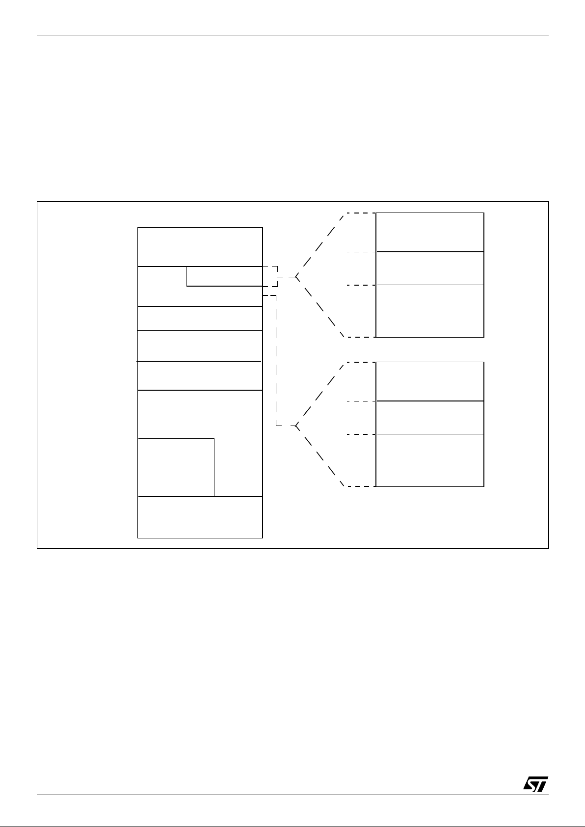
3 REGISTER & MEMORY MAP
As shown in Figure 11, the MCU is capable of addressing 64 Kbytes of memories and I/O registers.
The available memory locations consist of 80
bytes of register locations, up to 5 Kby tes of RA M
and up to 32 Kbytes of user program memory. The
RAM space includes u p to 256 by t es fo r the stack
from 0100h to 01FFh.
The highest address bytes contain the user re set
and interrupt vectors.
IMPORTANT: Memory locations noted “Reserved” must ne ver be accessed. Ac cessing a reserved area can have unpredictable effects on the
device.
Figure 11. Memory Map
* Program memory and RAM sizes are product dependent (see Table –)
** The ST7 core is not able to read or write in the USB data buffer if the ST7265x is running at 6Mz in stan-
dalone mode.
0000h
Interrupt & Reset Vectors
HW Registers
0050h
004Fh
(see Table 4)
FFDFh
FFE0h
FFFFh
(see Table 10)
8000h
7FFFh
Program Memory*
5 KBytes RAM*
16 Kbytes
C000h
Reserved
1450h
144Fh
32 Kbytes
512 Bytes RAM*
Short Addressing
Stack (256 Bytes)
0100h
0200h
144Fh
0050h
00FFh
01FFh
16-bit Addressing RAM
RAM (176 Bytes)
(4688 Bytes)
Short Addressing
Stack (256 Bytes)
0100h
0200h
024Fh
0050h
00FFh
01FFh
16-bit Addressing RAM
RAM (176 Bytes)
(80 Bytes)
154Fh
1A4Fh
256 Bytes
1280 Bytes
USB Data Buffer**
DTC RAM (Write protected)
1
ST7265x
19/166
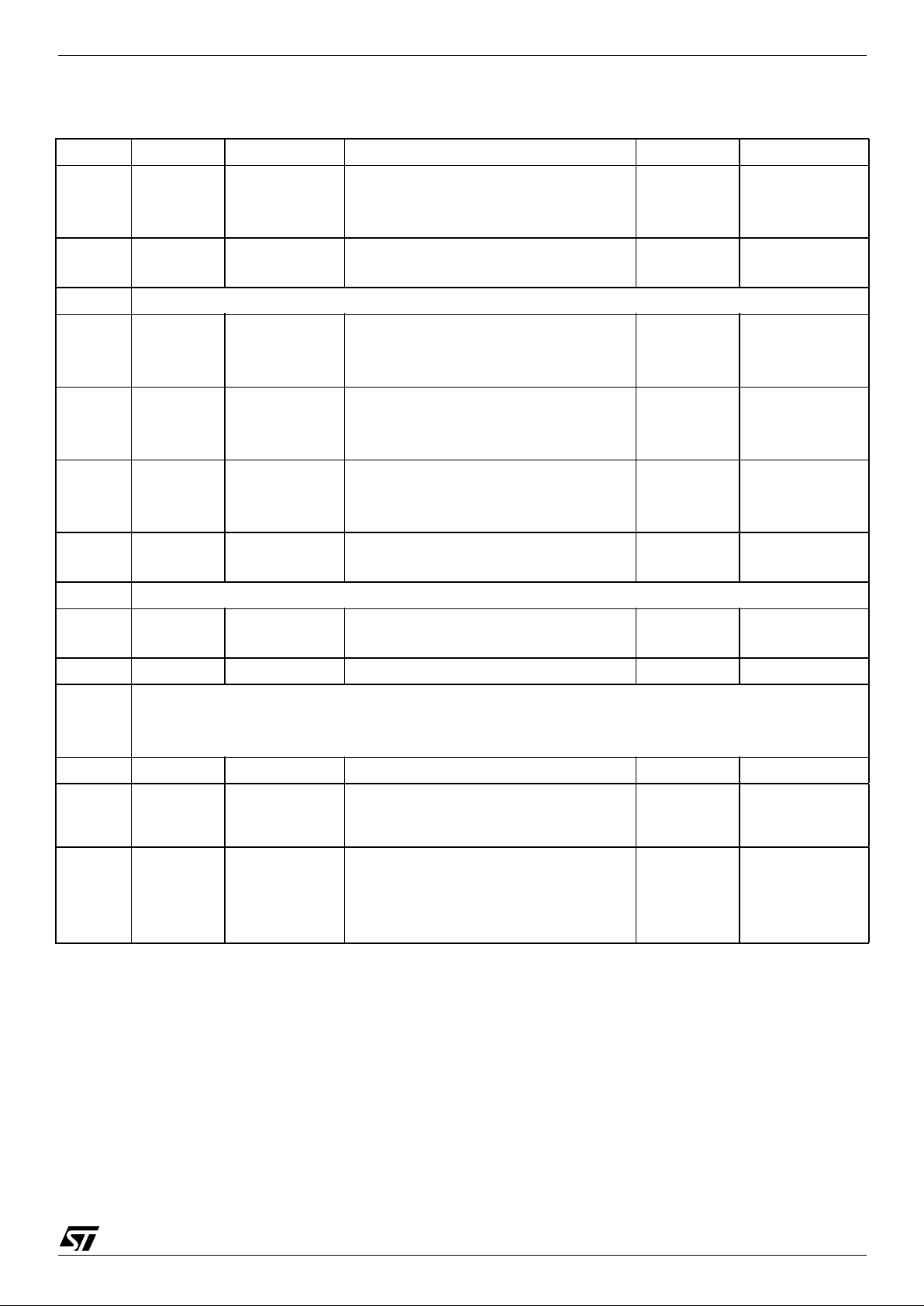
Table 4. Hardware Register Memory Map
Address Block Register Label Register name Reset Status Remarks
0000h
0001h
0002h
PADR
PADDR
PAOR
Port A Data Register
Port A Data Direction Register
Port A Option Register
00h
00h
00h
R/W
R/W
R/W
0003h
0004h
PBDR
PBDDR
Port B Data Register
Port B Data Direction Register
00h
00h
R/W
R/W
0005h Reserved Area (1 byte)
0006h
0007h
0008h
PCDR
PCDDR
PCOR
Port C Data Register
Port C Data Direction Register
Port C Option Register
00h
00h
00h
R/W
R/W
R/W
0009h
000Ah
000Bh
PDDR
PDDDR
PDOR
Port D Data Register
Port D Data Direction Register
Port D Option Register
00h
00h
00h
R/W
R/W
R/W
000Ch
000Dh
000Eh
PEDR
PEDDR
PEOR
Port E Data Register
Port E Data Direction Register
Port E Option Register
00h
00h
00h
R/W
R/W
R/W
000Fh
0010h
PFDR
PFDDR
Port F Data Register
Port F Data Direction Register
00h
00h
R/W
R/W
0011h Reserved Area (1 byte)
0012h
0013h
ADC
1
ADCDR
ADCCSR
ADC Data Register
ADC Control Status Register
00h
00h
Read only
R/W
0014h WDG WDGCR Watchdog Control Register 7Fh R/W
0015h
to
0017h
Reserved Area (3 bytes)
0018h DSM PCR Power Control Register 00h R/W
0019h
001Ah
001Bh
SPI
SPIDR
SPICR
SPICSR
SPI Data I/O Register
SPI Control Register
SPI Control/Status Register
xxh
0xh
00h
R/W
R/W
R/W
001Ch
001Dh
001Eh
001Fh
DTC
DTCCR
DTCSR
Reserved
DTCPR
DTC Control Register
DTC Status Register
DTC Pointer Register
00h
00h
00h
R/W
R/W
R/W
1

ST7265x
20/166
0020h
0021h
0022h
0023h
0024h
0025h
0026h
0027h
0028h
0029h
002Ah
TIM
TCR1
TCR2
TSR
CHR
CLR
ACHR
ACLR
OC1HR
OC1LR
OC2HR
OC2LR
Timer Control Register 1
Timer Control Register 2
Timer Status Register
Timer Counter High Register
Timer Counter Low Register
Timer Alternate Counter High Register
Timer Alternate Counter Low Register
Timer Output Compare 1 High Register
Timer Output Compare 1 Low Register
Timer Output Compare 2 High Register
Timer Output Compare 2 Low Register
00h
00h
00h
FFh
FCh
FFh
FCh
80h
00h
80h
00h
R/W
R/W
Read Only
Read Only
Read Only
Read Only
Read Only
R/W
R/W
R/W
R/W
002Bh Flash Flash Control Status Register 00h R/W
002Ch
002Dh
002Eh
002Fh
ITC
ITSPR0
ITSPR1
ITSPR2
ITSPR3
Interrupt Software Priority Register 0
Interrupt Software Priority Register 1
Interrupt Software Priority Register 2
Interrupt Software Priority Register 3
FFh
FFh
FFh
FFh
R/W
R/W
R/W
R/W
0030h
0031h
0032h
0033h
0034h
0035h
0036h
0037h
0038h
0039h
003Ah
003Bh
003Ch
003Dh
003Eh
003Fh
USB
USBISTR
USBIMR
USBCTLR
DADDR
USBSR
EP0R
CNT0RXR
CNT0TXR
EP1RXR
CNT1RXR
EP1TXR
CNT1TXR
EP2RXR
CNT2RXR
EP2TXR
CNT2TXR
USB Interrupt Status Register
USB Interrupt Mask Register
USB Control Register
Device Address Registe r
USB Status Register
Endpoint 0 Register
EP 0 Reception Counter Register
EP 0 Transmission Counter Register
Endpoint 1 Register
EP 1 Reception Counter Register
Endpoint 1 Register
EP 1 Transmission Counter Register
Endpoint 2 Register
EP 2 Reception Counter Register
Endpoint 2 Register
EP 2 Transmission Counter Register
00h
00h
06h
00h
00h
00h
00h
00h
00h
00h
00h
00h
00h
00h
00h
00h
R/W
R/W
R/W
R/W
R/W
R/W
R/W
R/W
R/W
R/W
R/W
R/W
R/W
R/W
R/W
R/W
0040h
0041h
0042h
0043h
0044h
0045h
0046h
I
2C 1
I2CCR
I2CSR1
I2CSR2
I2CCCR
Not used
Not used
I2CDR
I
2
C Control Register
I
2
C Status Register 1
I
2
C Status Register 2
I
2
C Clock Control Register
I
2
C Data Register
00h
00h
00h
00h
00h
R/W
Read only
Read only
R/W
R/W
0047h USB BUFCSR Buffer Control/Status Register 00h R/W
0048h Reserved Area (1 Byte)
0049h MISCR1 Miscellaneous Register 1 00h R/W
004Ah MISCR2 Miscellaneous Register 2 00h R/W
004Bh Reserved Area (1 Byte)
Address Block Register Label Register name Reset Status Remarks
1

ST7265x
21/166
Note 1. If the peripheral is present on the device (see Device Summary on page 1)
004Ch MISCR3 Miscellaneous Register 3 00h R/W
004Dh
004Eh
004Fh
PWM
1
PWM0
BRM10
PWM1
10-bit PWM/BRM registers
80h
00h
80h
R/W
R/W
R/W
Address Block Register Label Register name Reset Status Remarks
1

ST7265x
22/166
4 FLASH PROGRAM MEMORY
4.1 Introduc t ion
The ST7 dual voltage High Density Flash
(HDFlash) is a non-volatile memory that can be
electrically erased as a single block or by individual sectors and programmed on a Byte-by-Byte basis using an external V
PP
supply.
The HDFlash devices can be programmed and
erased off-board (plugge d in a programm ing tool)
or on-board using ICP (In-Circuit Programming) or
IAP (In-Application Programming).
The array matrix organ isation allows each sector
to be erased and reprogramm ed without affecting
other sectors.
4.2 Main Features
■ Three Flash programming modes:
– Insertion in a programming tool. In this m ode,
all sectors including option bytes can be programmed or erased.
– ICP (In-Circuit Programming). In this mode, all
sectors including option bytes can be programmed or erased without removing the device from the application board.
– IAP (In-Application Programming) In this
mode, all sectors except Sector 0, can be programmed or erased without removing the device from the application board a nd wh ile the
application is running.
■ ICT (In-Circuit Testing) for downloading and
executing user application test patterns in RAM
■ Read-out protection against piracy
■ Register Access Security System (RASS) to
prevent accidental programming or erasing
4.3 Structure
The Flash memory is organised in sectors and can
be used for both code and data storage.
Depending on the overall Flash memory size in the
microcontroller device, there are up to three user
sectors (see Table 5). Each of these sectors can
be erased independently to avoid unnecessary
erasing of the whole Flas h memory when only a
partial erasing is required.
The first two sectors have a fixed siz e of 4 Kby tes
(see Figure 12). They are mapped in the upper
part of the ST7 addressing space so the reset and
interrupt vectors are located in Sector 0 (F000hFFFFh).
Table 5. Sectors available in Flash devices
4.4 Program Memo ry Read-out Protecti on
The read-out protection is enabled through an option bit.
When this option is selected, the programs and
data stored in the program memory (Flash or
ROM) are protected against read-out piracy (including a re-write protection). In Flash devices,
when this protection is removed by reprogramming the Option Byte, th e entire program memory
is first automatically erased and the device can be
reprogrammed.
Refer to the Option By te description for more details.
Figure 12. Memory Map and Sector Address
Flash Memory Size
(bytes)
Available Sectors
4K Sector 0
8K Sectors 0,1
> 8K Sectors 0,1, 2
4 Kbytes
4 Kbytes
2Kbytes
SECTOR 1
SECTOR 0
16 Kbytes
SECTOR 2
8K 16K 32K 60K DV FLASH
FFFFh
EFFFh
DFFFh
3FFFh
7FFFh
1000h
24 Kbytes
MEMORY SIZE
8Kbytes 40 Kbytes
52 Kbytes
9FFFh
BFFFh
D7FFh
4K 10K 24K 48K
1
ST7265x
23/166
FLASH PROGRAM MEMORY (Cont’d)
4.5 ICP (In-Circuit Programming)
To perform ICP the microcontroller must be
switched to ICC (In-Circuit Communication) mode
by an external controller or programming tool.
Depending on the ICP code dow nloaded in RAM,
Flash memory programming can be fully customized (number of bytes to prog ram, program locations, or selection serial communication interface
for downloading).
When using an STMicroelectronics or third-party
programming tool that supp orts ICP and the specific microcontroller device, the user needs only to
implement the ICP hardware interface on the application board (see Figure 13). For more details
on the pin locations, refer to the device pinout description.
ICP needs six pins to be connected to the programming tool. These pins are:
– RESET
: device reset
–V
SS
: device power supply ground
– ICCCLK: ICC output serial clock pin
– ICCDATA: ICC input serial data pin
– ICCSEL/V
PP
: programming voltage
–V
DD
: application board power supply
CAUTIONS:
1. If RESET
, ICCCLK or ICCDATA pins are used
for other purposes in the application, a serial resistor has to be implemented to avoid a conflict in
case one of the other devices forces the signal level. If these pins are used as outputs in the application, the serial resistors are not necessary. As
soon as the external controller is plugged to the
board, even if an ICC sess ion is not in progress,
the ICCCLK and ICC DATA pins are not available
for the application.
2. The use of Pin 7 of the ICC con nector de pends
on the Programming Tool architecture. Please refer to the documentatio n of the tool. This pi n m ust
be connected when using ST Prog ramming Tools
(it is used to monitor the application power supply).
Note: To develop a custom program ming t ool, refer to the ST7 Flash Programming and ICC Reference Manual which gives full details on the ICC
protocol hardware and software.
Figure 13. Ty pi c al IC P Int erf ace
ICC CONNECTOR
ICCDATA
ICCCLK
RESET
VDD
HE10 CONNECTORTYPE
>4.7kΩ
APPLICATION
POWER SUPPLY
OPTIONAL (SEE CAUTION 1)
1
246810
975 3
PROGRAMMING TOOL
ICC CONNECTOR
APPL ICATION BOAR D
ICC C a ble
OPTIONAL
(SEE CA UTION 2)
10kΩ
VSS
ICCSEL/VPP
ST7
1

ST7265x
24/166
FLASH PROGRAM MEMORY (Cont’d)
4.6 IA P ( I n-Applicatio n P rogramm i ng)
This mode uses a BootLoader program previously
stored in Sector 0 by the us er (in ICP mode or by
plugging the device in a programming tool).
This mode is fully controlled by user software. This
allows it to be adapted to the user application, (user-defined strategy for entering programming
mode, choice of comm unications protocol used to
fetch the data to be stored, etc.). For example, it is
possible to download code from the SPI, SCI, USB
or CAN interface and program it in the Fl ash. IAP
mode can be used to program any of the Flash
sectors except Sector 0, which is write/erase protected to allow recovery in case errors occur during the programming operation.
4.7 Related Documentation
For details on Flash program ming and I CC protocol, refer to the ST7 Flash Programming Reference Manual and to the ST7 ICC Protocol Reference Manual
.
4.8 Register Description
FLASH CONTROL/STATUS REGISTER (FCSR)
Read/Write
Reset Value: 0000 0000 (00h)
This register is reserved for use by Programming
Tool software. It controls the Flash programming
and erasing operations.
Table 6. FLASH Register Map and Reset Values
70
00000000
Address
(Hex.)
Register
Label
76543210
002Bh
FCSR
Reset Value
00000000
1

ST7265x
25/166
5 CENTRAL PRO CESSING UNIT
5.1 INTRODUCTION
This CPU has a full 8-bit architecture and contains
six internal registers allowing efficient 8-bit data
manipulation.
5.2 MAIN FEATURES
■ Enable executing 63 basic instructions
■ Fast 8-bit by 8-bit multiply
■ 17 main addressing modes (with indirect
addressing mode)
■ Two 8-bit index registers
■ 16-bit stack pointer
■ Low power HALT and WAIT modes
■ Priority maskable hardware interrupts
■ Non-maskable software/hardware interrupts
5.3 CPU REGISTERS
The 6 CPU registers shown in Figu re 14 are not
present in the memory mapping and are accessed
by spec ifi c ins t ru c tio n s .
Accumulator (A)
The Accumulator is an 8-bit general purpose register used to hold operands and the res ults of the
arithmetic and logic calculations and to manipulate
data.
Index Registers (X and Y)
These 8-bit registers are used to create effective
addresses or as tempo rary storage areas f or data
manipulation. (The Cross -Assembler generates a
precede instruction (PRE) to indicate that the following instruction refers to the Y register.)
The Y register is not affected by the interrupt automatic procedures.
Program Counter (PC)
The program counter is a 16-bit register containing
the address of the next instruction to be executed
by the CPU. It is made of two 8-bit registers PCL
(Program Counter Low which is the LSB) and PCH
(Program Counter High which is the MSB).
Figure 14. CPU Registers
ACCUMULATOR
X INDEX REGISTER
Y INDEX REGISTER
STACK POINTER
CONDITION CODE REGISTER
PROGRAM COUNTER
70
1C1I1HI0NZ
RESET VALUE = RESET VECTOR @ FFFEh-FFFFh
70
70
70
0
7
15 8
PCH
PCL
15
8
70
RESET VALUE = STACK HIGHER ADDRESS
RESET VALUE =
1X11X1XX
RESET VALUE = XXh
RESET VALUE = XXh
RESET VALUE = XXh
X = Undefined Value
1

ST7265x
26/166
CENTRAL PROC ESSING UNIT (Cont’d)
Condition Code Register (CC)
Read/Write
Reset Value: 111x1xxx
The 8-bit Condition Code regist er contains the i nterrupt masks and four flags representative of the
result of the instruction just executed. This register
can also be handled by the PUSH and POP instructions.
These bits can be individually tested and/or controlled by specific instructions.
Arithmetic Management Bits
Bit 4 = H
Half carry
.
This bit is set by hardware when a carry occurs between bits 3 and 4 of t he ALU during an ADD or
ADC instructions. It is reset by hardware during
the same instructio n s.
0: No half carry has occurred.
1: A half carry has occurred.
This bit is tested using the JRH or JRNH instruction. The H bit is useful in BCD arithmetic subroutine s .
Bit 2 = N
Negative
.
This bit is set and cleared by hardware. It is representative of the result sign of the last arithmetic,
logical or data manipulation. I t’s a copy of the result 7
th
bit.
0: The result of the last operation is positive or null.
1: The result of the last operation is negative
(i.e. the most significant bit is a logic 1).
This bit is accesse d by the JRMI and JRPL instructions.
Bit 1 = Z
Zero
.
This bit is set and cleared by hardware. This bit indicates that the result of the last arithmetic, logical
or data manipulation is zero.
0: The result of the last operation is different from
zero.
1: The result of the last operation is zero.
This bit is accessed by the JREQ and JRNE test
instructions.
Bit 0 = C
Carry/borrow.
This bit is set and cleared b y hardware and software. It indicates an overflow or an un derflow has
occurred during the last arithmetic operation.
0: No overflow or underflow has occurred.
1: An overflow or underflow has occurred.
This bit is driven by the SCF and RCF instructions
and tested by the JRC and JRNC instructions. It i s
also affected by the “bit test and branch”, shift and
rotate instructions.
Interrupt Managem ent B i ts
Bit 5,3 = I1, I0
Interrupt
The combination of the I1 and I0 bits gives the current interrupt software priority.
These two bits are set/cleared by hardware when
entering in interrupt. The loaded value is given by
the corresponding bits in the interrupt software priority registers (IxSPR). They can be also set/
cleared by software with the RIM, SIM, IRET,
HALT, WFI and PUSH/POP instructions.
See the interrupt management chapter for more
details.
70
11I1HI0NZ
C
Interrupt Software Priorit y I1 I0
Level 0 (main) 1 0
Level 1 0 1
Level 2 0 0
Level 3 (= interrupt disable) 1 1
1

ST7265x
27/166
CENTRAL PROC ESSING UNIT (Cont’d)
Stack Poi nter (SP)
Read/Write
Reset Value: 01 FFh
The Stack Pointer is a 16-bit register which is always pointing to the next free location in the stack.
It is then decremented after data has been pushed
onto the stack and incremented before data is
popped from the stack (see Figure 15).
Since the stack is 256 bytes deep, the 8 most significant bits are forced by hard ware. Following a n
MCU Reset, or after a Reset Stack Pointer instruction (RSP), the Stack Pointer contains its reset value (the SP7 to SP0 bits are set) which is the stack
higher address.
The least significant byte of the Stack Pointer
(called S) can be directly accessed by a LD instruction.
Note: When the lower limit is exceeded, the Stack
Pointer wraps around to the stack upper limit, without indicating the stack overflow. The previously
stored information is then o verwritten and therefore lost. The stack also wraps in case of an underflow.
The stack is used to sav e the return address during a subroutine call and the CPU context during
an interrupt. The user may also directly manipulate
the stack by means of the PUSH and POP instructions. In the case of an interrupt, the PCL is stored
at the first location po inted t o by t he SP. Th en t he
other registers are stored in the next locations as
shown in Figure 15.
– When an interrupt is received, the SP is decre-
mented and the context is pushed on the stack.
– On return from interrupt, the SP is incremented
and the context is popped from the stack.
A subroutine call occupies two locations and an interrupt five locat ion s i n the stack ar ea.
Figure 15. Stack Manipulation Examp le
15 8
00000001
70
SP7 SP6 SP5 SP4 SP3 SP2 SP1
SP0
PCH
PCL
SP
PCH
PCL
SP
PCL
PCH
X
A
CC
PCH
PCL
SP
PCL
PCH
X
A
CC
PCH
PCL
SP
PCL
PCH
X
A
CC
PCH
PCL
SP
SP
Y
CALL
Subroutine
Interrupt
Event
PUSH Y POP Y IRET
RET
or RSP
@ 01FFh
@ 0100h
Stack Higher Address = 01FFh
Stack Lower Address =
0100h
1
ST7265x
28/166
6 SUPPLY, RESET AND CLOCK MANAGEMENT
6.1 CLOCK SYSTEM
6.1.1 General Description
The MCU accepts either a 12 MHz crystal or an
external clock signal to drive the internal oscillator.
The internal clock (f
CPU
) is derived from the inter-
nal oscillator frequency (f
OSC
), which is 12 Mhz in
Stand-alone mode and 48M hz in USB mode.
The internal clock (f
CPU
) is software selectable using the CP[1:0] and CPEN bits in the MISCR1 register.
In USBV
DD
power supply mode, the PLL is active,
generating a 48MHz clock to the USB. In this
mode, f
CPU
can be configured to be up to 8 MHz.
In V
DD
mode the PLL and the USB clock are disa-
bled, and the maximum frequency of f
CPU
is 6
MHz.
The internal clock signal (f
CPU
) is also routed to
the on-chip peripherals. The CPU clock signal
consists of a square wave with a duty cycle of
50%.
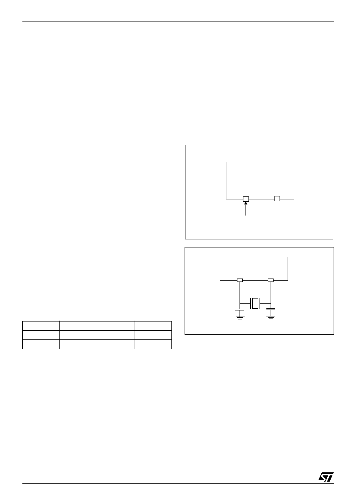
The internal oscillat or is designed to operate with
an AT-cut parallel resonant quartz in the frequency
range specified for f
osc
. The circuit shown in Fig-
ure 17 is recommended when using a crystal, and
Table 7 lists the recommen ded capacitance. The
crystal and associated components should be
mounted as close as p ossible to the input pins i n
order to minimize output distortion and start-up
stabilisation time.
Table 7. Recom m ended Values for 12-MHz
Crystal Resonator
Note: R
SMAX
is the equivalent serial resistor of the
crystal (see crystal specification).
6.1.2 External Clock
An external clock may be applied to the OSCIN input with the OSCOUT pin not connected, as
shown on Figure 16. The t
OXOV
specifications
does not apply when using an external clock input.
The equivalent spe cification of the external c lock
source should be used instead of t
OXOV
(see Sec-
tion 6.5 CONTROL TIMING).
Figure 16. External Clock Source Connections
Figure 17. Crystal Resonator
R
SMAX
20 Ω 25 Ω 70 Ω
C
OSCIN
56pF 47pF 22pF
C
OSCOUT
56pF 47pF 22pF
OSCIN OSCO UT
EXTERNAL
CLOCK
NC
OSCIN OSCOUT
C
OSCIN
C
OSCOUT
1

ST7265x
29/166
6.2 RESET SEQUENCE MANAGER (RSM)
6.2.1 Introd uc tion
The reset sequence manager in cludes three RESET sources as shown in F igure 6.2.2:
■ External RESET source pulse
■ Internal LVD RESET (Low Voltage Detection)
■ Internal WATCHDOG RESET
These sources act on the RESET
pin and it is al-
ways kept low during the delay phase.
The RESET service routine vector is fixed at addresses FFFEh-FFFFh in the ST7 memory map.
The basic RESET sequence consists of 3 phases
as shown in Figure 18:
■ Active Phase depending on the RESET source
■ Min 512 CPU clock cycle delay (see Figure 20
and Figure 21
■ RESET vector fet ch
Figure 18. RESET Sequences
V
DD
RUN
RESET PIN
EXTERNAL
WATCHDOG
ACTIVE PHASE
V
IT+(LVD)
V
IT-(LVD)
t
h(RSTL)in
t
w(RSTL)out
RUN
t
h(RSTL)in
ACTIVE
WATCHDOG UNDERFLOW
t
w(RSTL)out
RUN RUN RUN
RESET
RESET
SOURCE
SHORT EXT.
RESET
LVD
RESET
LONG EXT.
RESET
WATCHDOG
RESET
INTERNAL RESET(min 512T
CPU
)
VECTOR FETCH
t
w(RSTL)out
PHASE
ACTIVE
PHASE
ACTIVE
PHASE
DELAY
1
ST7265x
30/166
RESET SEQUENCE MANAGER (Cont’d)
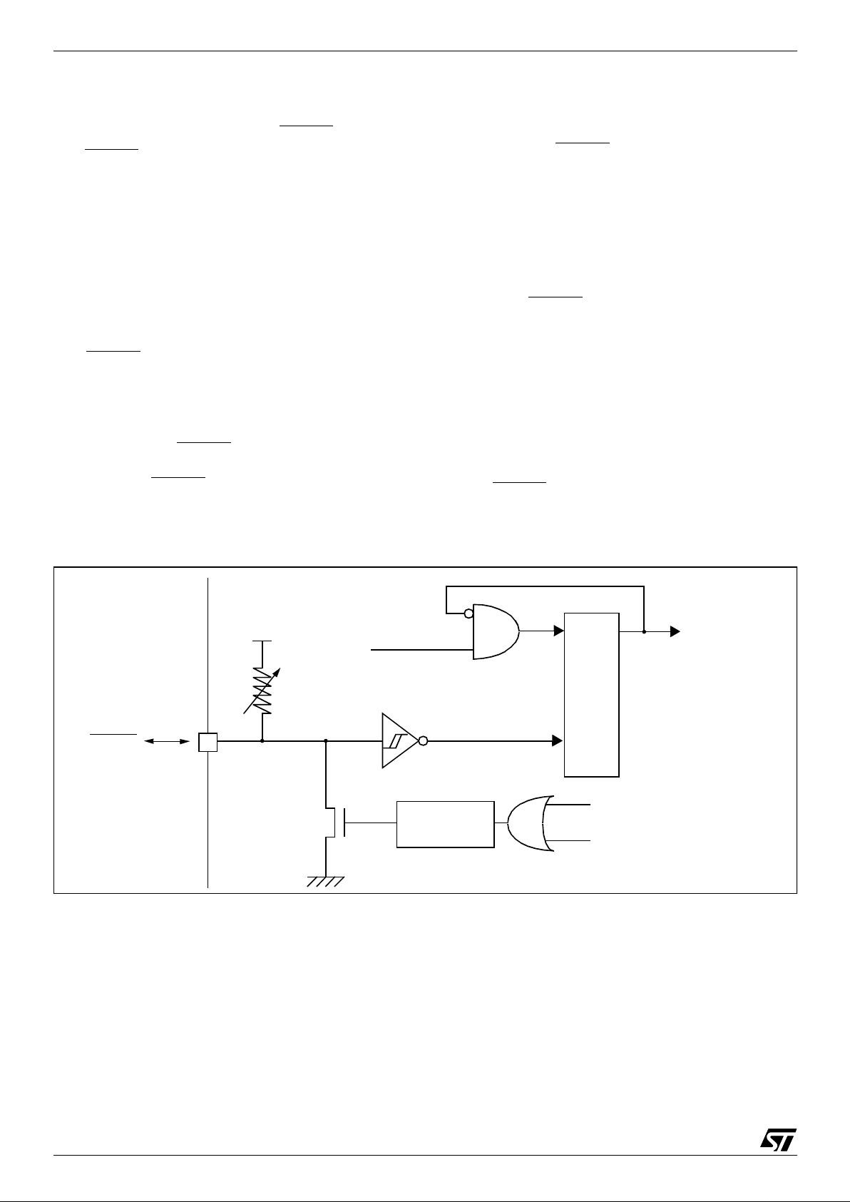
6.2.2 Asynchronous External RES ET
pin
The RESET
pin is both an input and an open-drain
output with integrated R
ON
weak pull-up resistor.
This pull-up has no fixed value but varies in accordance with the input voltage. It
can be pulled
low by external circuitry to reset the device. See
electrical characteristics section for more details.
A RESET signal originating from an external
source must have a duration of at least t
h(RSTL)in
in
order to be recognized. This detection is asynchronous and therefore the MCU can enter reset state
even in HALT mode.
The RESET
pin is an asynchronous signal which
plays a major role in EMS performance. In a noisy
environment, it is recommended to follow the
guidelines mentioned in the elect rical characteristics section.
If the external RESET
pulse is shorter than
t
w(RSTL)out
(see short ext. Reset in Figure 18), the
signal on the RESET
pin will be stretch ed. Other wise the delay will not be applied (see long ext.
Reset in Figure 18).
Starting from the external RE SET pulse recognition, the device RESET
pin acts as an output that
is pulled low during at least t
w(RSTL)out
.
6.2.3 Int e r na l Lo w Volta ge Detection RESET
Two differe nt RESET sequences caused by the internal LVD circuitry can be distinguished:
■ Power-On RESET
■ Voltage Drop RESET
The device RESET
pin acts as an output that is
pulled low when V
DD<VIT+
(rising edge) or
V
DD<VIT-
(falling edge) as shown in Figure 18.
The LVD filters spikes on V
DD
shorter than t
g(VDD)
to avoid parasitic resets.
6.2.4 Internal Watchdog RESET
The RESET sequence generated by a internal
Watchdog counter overflow is shown in Figure 18.
Starting from the Watchdog counter underflow, the
device RESET
pin acts as an output that is pulled
low during at least t
w(RSTL)out
.
Figure 19. Reset Block Diagram
f
CPU
COUNTE R
RESET
R
ON
V
DD
WATCHDOG RESET
LVD RESET
INTERNAL
RESET
PULSE
GENERATO R
1
 Loading...