

SGS Thomson Microelectronics LM323T, LM223K, LM123K, LM323K Datasheet
LM123/LM223
LM323
March1993
THREE-TERMINAL 3A-5V POSITIVE VOLTAGE REGULATORS
.OUTPUT CURRENT : 3A
.INTERNAL CURRENT AND THERMAL LIMI-
TING
.TYPICALOUPUT IMPEDANCE : 0.01Ω
.MINIMUMINPUT VOLTAGE: 7.5V
.POWER DISSIPATION : 30W
DESCRI PTIO N
The LM123, LM223,LM323arethree-terminalpositive voltageregulators with a preset 5V output and
a load driving capability of 3A. New circuit design
and processing techniques areused to provide the
highoutputcurrent withoutsacrificing theregulation
characteristics of lower current devices.
The 3A regulator is virtually blowout proof.
Current limiting, power limiting and thermal shut-
down provide the same high level of reliability obtainedwith thesetechniques in theLM209, 1Aregulator.
An overallworstcasespecificationforthecombined
effects of input voltage, load current, ambient temperature, and power dissipation ensure that the
LM123,LM223,LM323 will performsatisfactorily as
a system element.
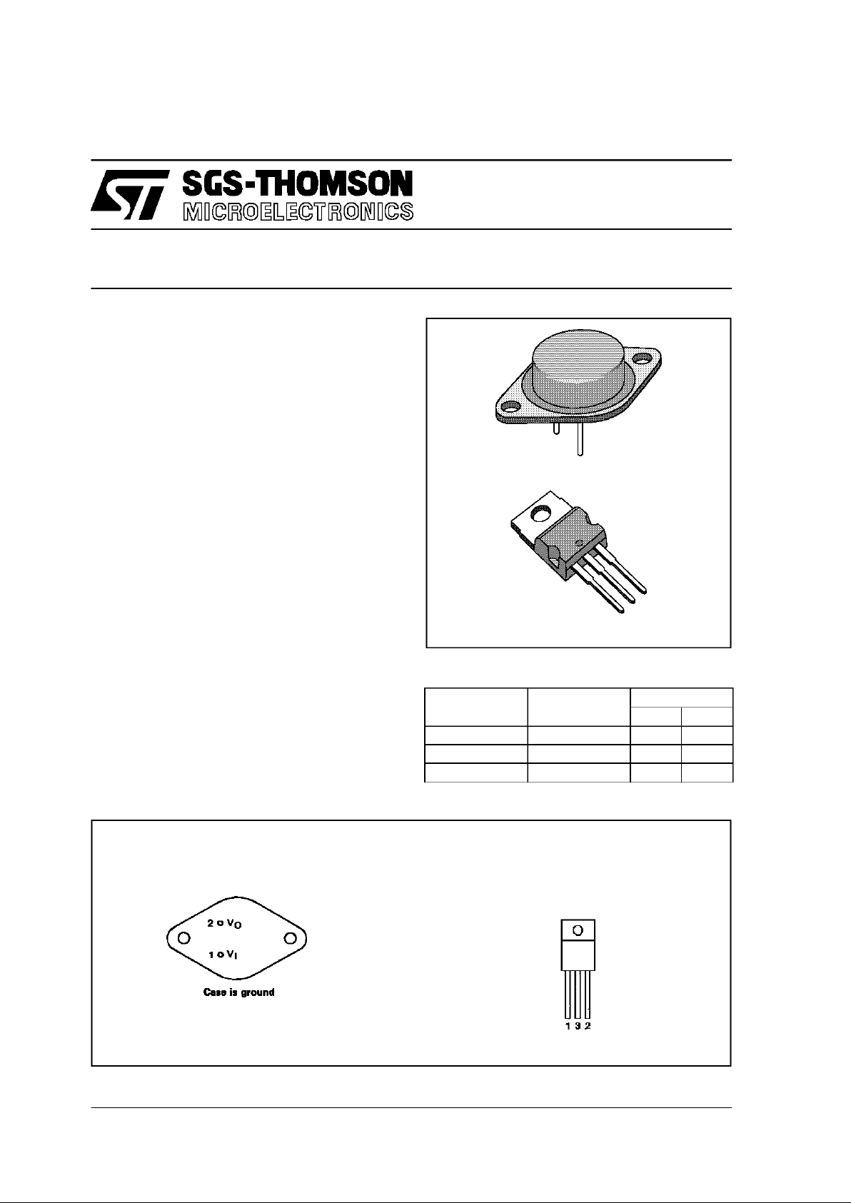
TO-3
PIN CONNEC TI ON
1 - Input
2 - Output
TO-3
(bot t om view)
ORDER CODES
Part Number Temperature
Range
Package
KT
LM123 -55
o
C to 150oC •
LM223 -25
o
C to 150oC •
LM323 0
o
C to 125oC ••
TO-220
TO-220
(front view)
1 - Input
2 - Output
3 - GND
1/9
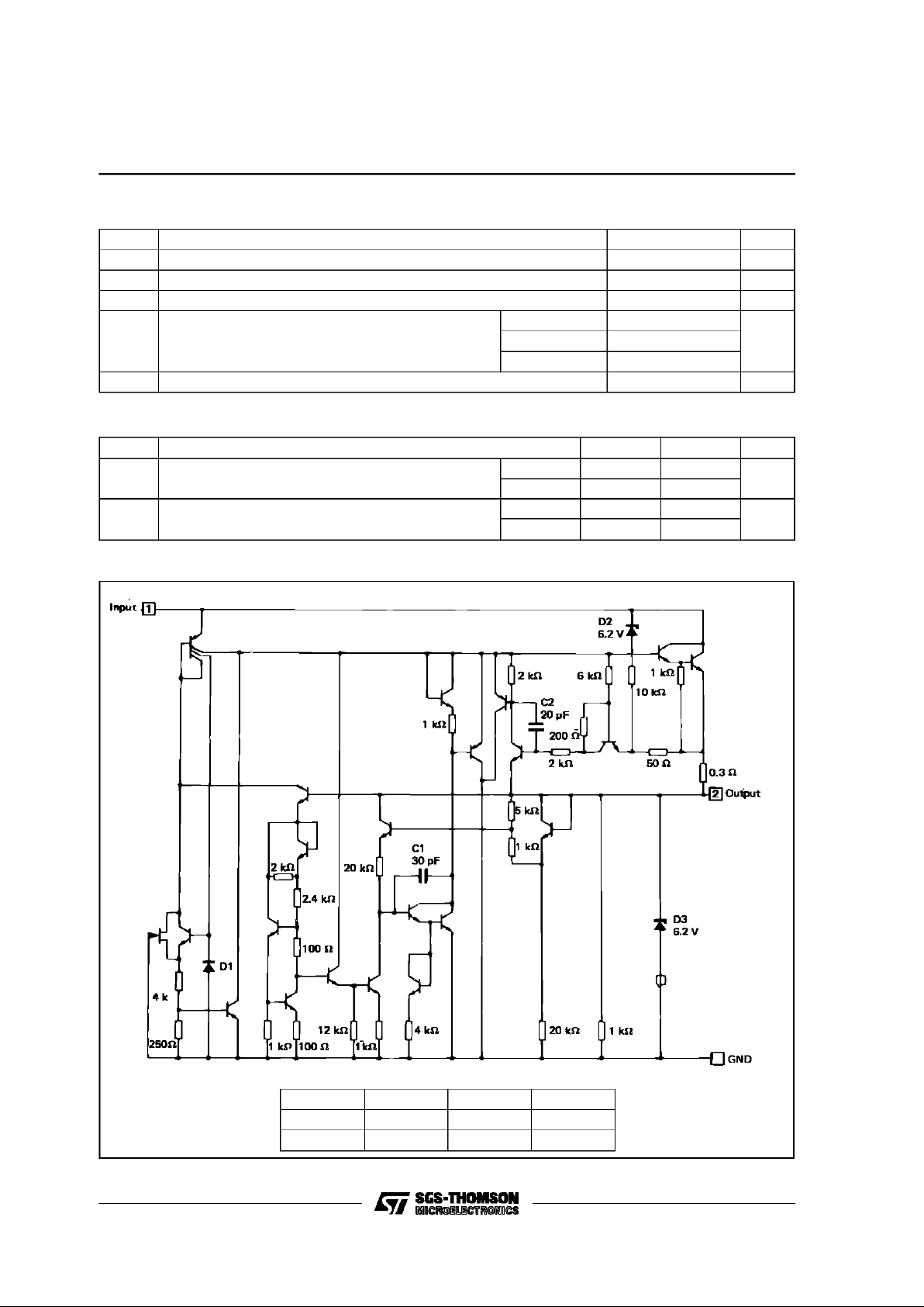
SCHEM ATIC D IA G RA M
Case VI VO GND
TO-3 1 2 Case
TO-220 1 2 3
ABSOLU TE MAXIMU M RAT ING
Symbol Parameter Value Unit
V
I
Input Voltage 20 V
I
O
Output Current Internally Limited
P
tot
Power Dissipation Internally Limited
T
oper
Operating Junction Temperature Range LM123 -55 to 150
o
C
LM223 -25 to 150
LM323 0 to 125
T
stg
Storage Temperature Range -65 to 150
o
C
THERMA L CHA R ACTER I STI CS
Symbol Parameter Typ. Max. Unit
R
thj-case
Junction-case Thermal Resistance TO-3 2
o
C/W
TO-220 3
R
thj-amb
Junction-ambient Thermal Resistance TO-3 35
o
C/W
TO-220 50
LM123-LM223-LM323
2/9
ELECTRIC AL CH A RAC TERI SIC S
LM123: -55oC<Tj<150oC
LM223: -25oC<Tj<150oC
LM323: 0oC<Tj<150oC
Symbol Parameter LM123/LM223 LM323 Unit
Min. Typ. Max. Min. Typ. Max.
V
O
Output Voltage Range (Note 2)
T
amb
=25oC, VI= 7.5 V, IO=0
4.7 5 5.3 4.8 5 5.2 V
V
O
Output Voltage Range (Note 2)
T
min
≤ Tj≤ T
max
,P≤P
max
7.5 V ≤ VI≤ 15 V, 0 ≤ IO≤ 3A
4.6 5.4 4.75 5.25 V
K
VI
Line Regulation (Note 3)
Tj=25oC, 7.5 V ≤ VI≤ 15V
5 25 5 25 mV
K
VO
Load Regulation (Note 3)
Tj=25oC, VI= 7.5 V, 0 ≤ IO≤ 3A
25 100 25 100 mV
I
IB
Quiescent Current
7.5 V ≤ V
I
≤ 15 V, 0 ≤ IO≤ 3A
12 20 12 20 mA
V
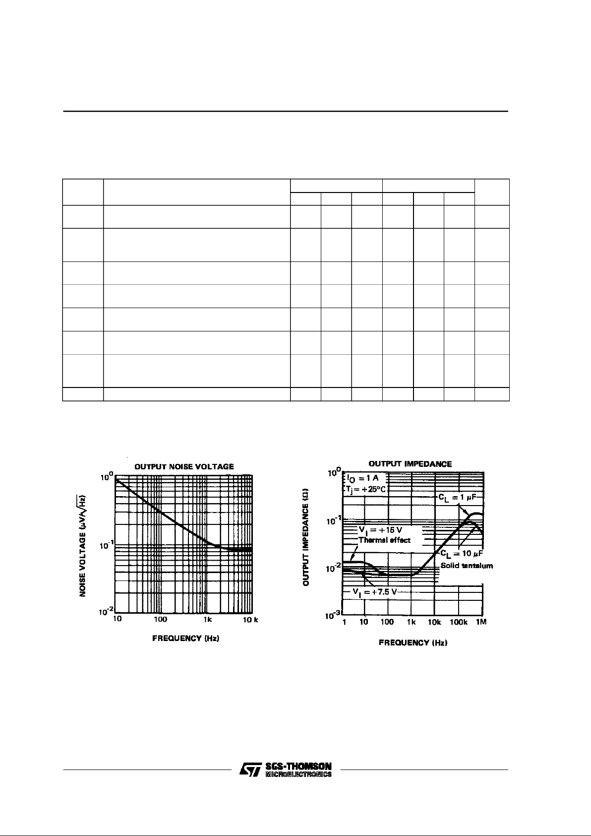
NO
Output Noise Voltage
T
amb
=25oC, 10 Hz ≤ f ≤ 100 KHz
40 40 µV
rms
I
OS
Short Circuit Current Limit (Tj=25oC)
VI=15V
VI= 7.5V
3
4
4.5
5
3
4
4.5
5
A
A
K
VH
Long Term Stability 35 35 mV
Notes : 1. Although power dissipation is internally limited, specifications apply only for P ≤ 30W.
2. Selected devices with tightened tolerance output voltage available.
3. Load and line regulation are specified at constant junction temperature. Pulse testing is required with a pulse width
≤ 1ms and a duty cycle ≤ 5%.
LM123-LM223-LM323
3/9
 Loading...