

1.2VTO 37V ADJUSTABLE VOLTAGE REGULATOR
.OUTPUT VOLTAGE RANGE :1.2 TO37V
.OUTPUT CURRENT INEXCESSOF 100 mA
.LINE REGULATIONTYP. 0.01%
.LOAD REGULATION TYP. 0.1%
.THERMALOVERLOAD PROTECTION
.SHORT CIRCUIT PROTECTION
.OUTPUT TRANSISTOR SAFE AREA COM-
PENSATION
.FLOATINGOPERATIONFOR HIGHVOLTAGE
APPLICATIONS
DESCRIPT ION
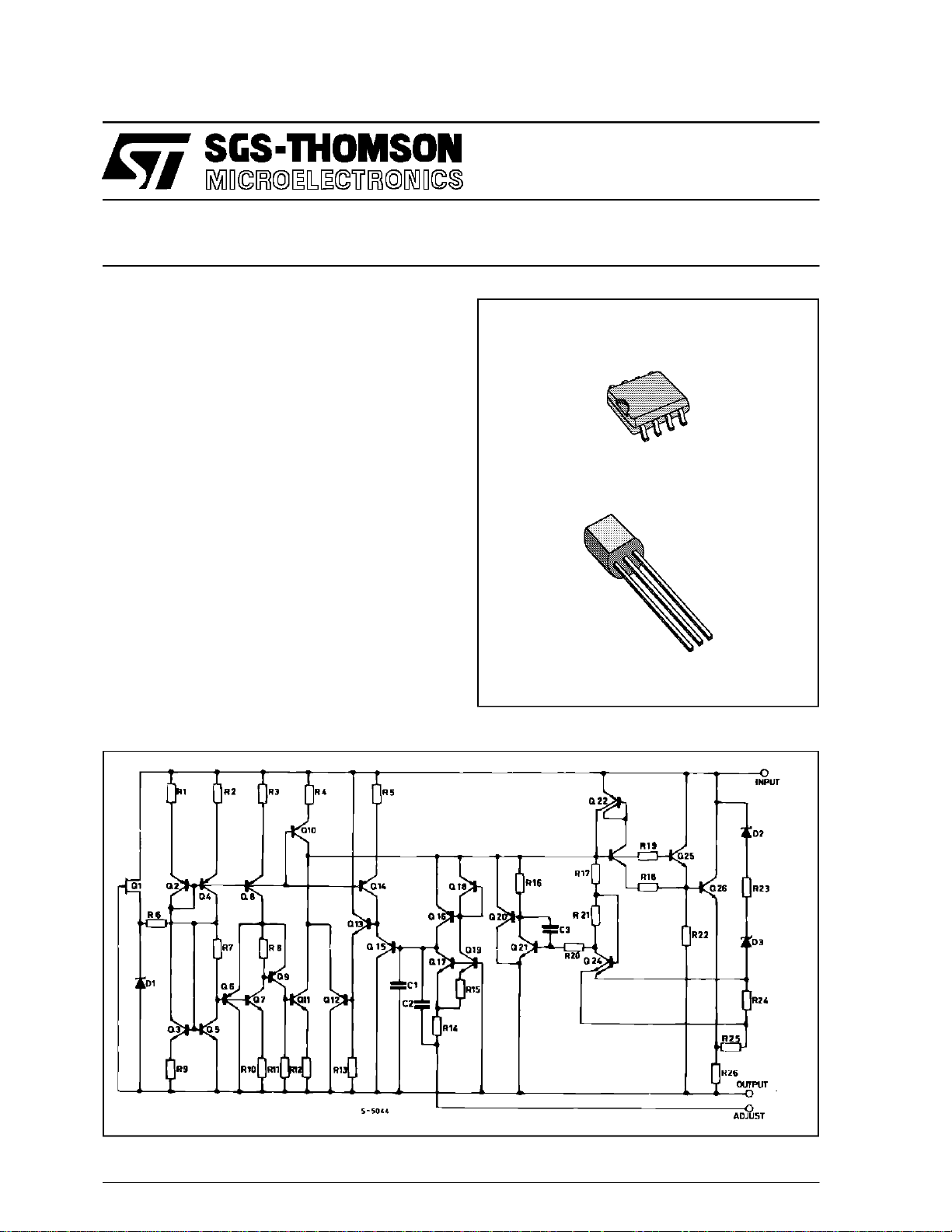
The LM217L/LM317L are monolithic integrated circuit in SO-8and TO-92packagesintended foruse
as positiveadjustable voltage regulators.
They are designed to supply until 100 mA of load
current with anoutput voltageadjustableover a 1.2
to 37V range.
The nominal output voltage is selected bymeans of
only a resistive divider, making the device exceptionally easy to use and eliminating the stockingof
many fixed regulators.
LM217L
LM317L
LOW CURRENT
SO-8
TO-92
SCHEM ATIC D IA G RA M
April1994
1/8
LM217L/LM317L
ABSOLUTE MAXIMUM RAT ING
Symbol Parameter Value Unit
V
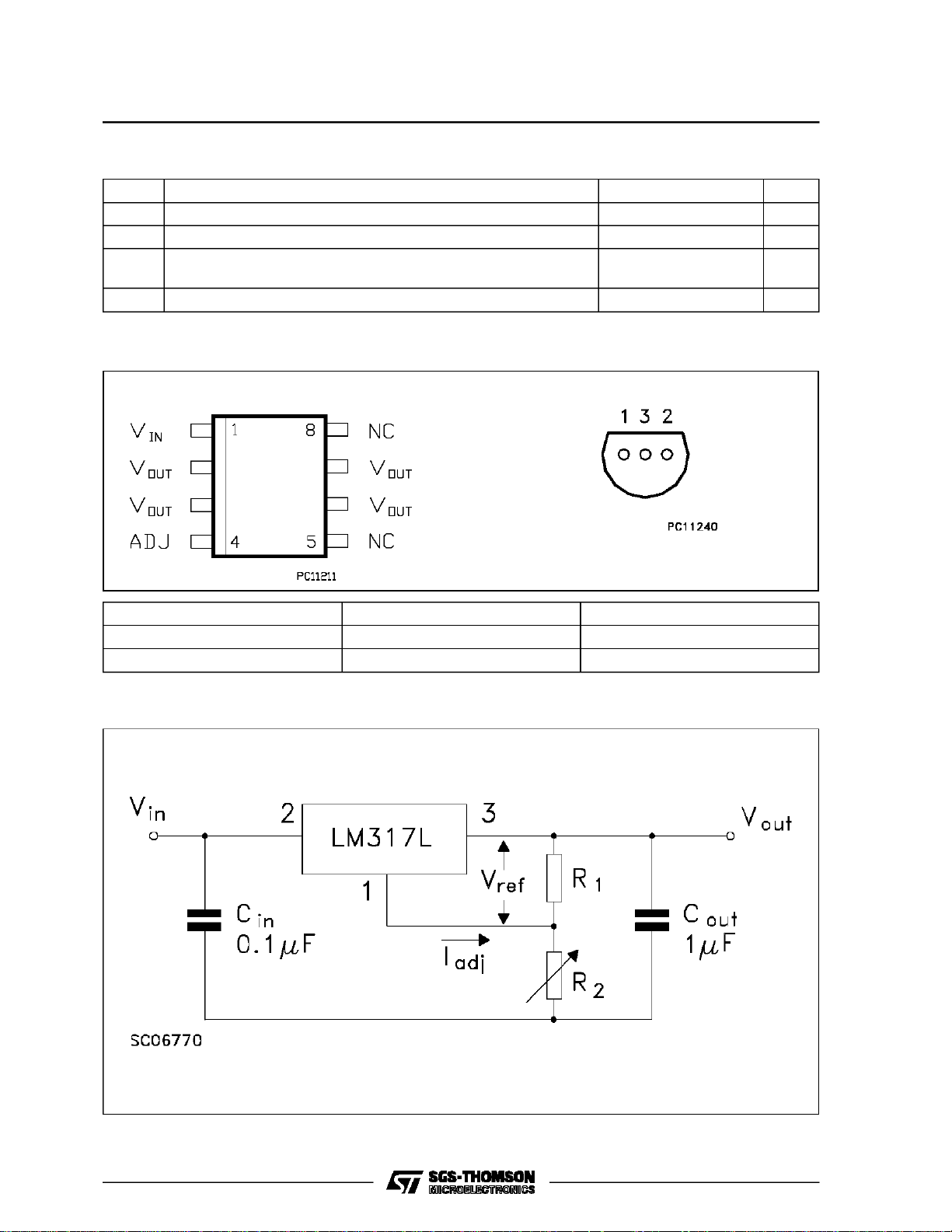
PIN CONNEC TION AND OR DE RI NG N U MBER
Input-Output Differential Voltage 40 V
i-Vo
Power Dissipation Internally Limited
P
d
Operating Junction Temperature Range for LM217L
T
opr
for LM317L
Storage Temperature Range -55 to 150
T
stg
-40 to 125
0 to 125
SO-8 TO-92
pin 1 = ADJUST
pin 2 = IN
pin 3 = OUT
BOTTOM VIEW
o
C
o
C
o
C
Type SO-8 TO-92
LM217L LM217LD LM217LZ
LM317L LM317LD LM317LZ
TEST CIRCUIT
2/8
LM217L / LM 3 17L
ELECT R I CAL CHARACT ER I STICS FOR LM 217L (Refer to t he test circ ui ts, -40 ≤ Tj≤ 125oC
Vi-Vo=5V,Io= 40 mA, unless otherw is e s pecified)
Symbol Parameter Test Conditions Min. Typ. Max. Unit
∆V
Line Regulation Vi-Vo= 3 to 40 V
o
IL<20mA
∆V
Load Regulation Vo≤ 5V
o
Io= 5 mA to 100 mA
V
≥ 5V
o
Io= 5 mA to 100 mA
I
Adjustment Pin Current 50 100 µA
ADJ
∆I
Adjustment Pin Current Vi-Vo= 3 to 40 V
ADJ
Io= 5 mA to 100 mA Pd< 625 mW
V
Reference Voltage Vi-Vo= 3 to 40 V
REF
Io= 5 mA to 100 mA Pd< 625 mW
∆
V
Output Voltage Temperature
o
Stability
V
o
I
I
o(max)
Minimum Load Current Vi-Vo= 40 V 3.5 5 mA
o(min)
Maximum Output Current Vi-Vo= 3 to 13 V
Vi-Vo=40V
e
Output Noise Voltage
N
(percentance of V
)
O
SVR Supply Voltage Rejection (*) T
B = 10Hz to 10KHz
Tj=25oC
=25oC
j
f = 120 Hz
(*) CADJ is connected between Adjust pin and Ground.
Tj=25oC 0.01 0.02 %/V
0.02 0.05 %/V
Tj=25oC 5 15 mV
20 50 mV
Tj=25oC 0.1 0.3 %
0.3 1 %
0.2 5 µA
1.2 1.25 1.3 V
0.7 %
100 200
mA
50
0.003 %
C
=0 65 dB
ADJ
C
=10µF66 80 dB
ADJ
ELECT R I CAL CHARACT ER I STICS FOR LM 317L (Refer to t he test circ ui ts, 0 ≤ Tj≤ 125oC
Vi-Vo=5V,Io= 40 mA, unless otherw is e s pecified)
Symbol Parameter Test Conditions Min. Typ. Max. Unit
∆V
Line Regulation Vi-Vo= 3 to 40 V
∆I
o
∆V
Load Regulation Vo≤ 5V
o
I
Adjustment Pin Current 50 100 µA
ADJ
Adjustment Pin Current Vi-Vo= 3 to 40 V
ADJ
I
<20mA
L
I
= 5 mA to 100 mA
o
V
≥ 5V
o
I
= 5 mA to 100 mA
o
Io= 5 mA to 100 mA Pd< 625 mW
V
Reference Voltage Vi-Vo= 3 to 40 V
REF
Io= 5 mA to 100 mA Pd< 625 mW
∆
V
Output Voltage Temperature
o
Stability
V
o
I
I
o(max)
Minimum Load Current Vi-Vo= 40 V 3.5 5 mA
o(min)
Maximum Output Current Vi-Vo= 3 to 13 V
Vi-Vo=40V
e
Output Noise Voltage
N
(percentance of VO)
SVR Supply Voltage Rejection (*) T
B = 10Hz to 10KHz
Tj=25oC
=25oC
j
f = 120 Hz
(*) CADJ is connected between Adjust pin and Ground.
=25oC 0.01 0.04 %/V
T
j
0.02 0.07 %/V
=25oC 5 25 mV
T
j
20 70 mV
=25oC 0.1 0.5 %
T
j
0.3 1.5 %
0.2 5 µA
1.2 1.25 1.3 V
0.7 %
100 200
50
0.003 %
C
=0 65 dB
ADJ
C
=10µF66 80 dB
ADJ
mA
3/8
 Loading...