


SAMSUNG TXJ2060, TXJ2754, TXJ2066, TXJ2067, TXJ2767 Service Manual
...
COLOR TELEVISION RECEIVER
Chassis : |
K51A |
|
Model: |
TXJ2060 |
TXJ2754 |
|
TXJ2066 |
TXJ2766 |
|
TXJ2067 |
TXJ2767 |
|
TXJ2554 |
TXJ2768 |
|
TXJ2566 |
TXJ2879 |
|
TXJ2567 |
|
COLOR TELEVISION RECEIVER |
|
CONTENTS |
1. Precautions
2. Specifications and IC Data
3. Alignment and Adjustments
4. Troubleshooting
5. Exploded Views and Parts List
6. Electric Parts List
7. Block Diagrams
8. Schematic Diagrams

ELECTRONICS
©Samsung Electronics Co., Ltd. APR.1999 Printed in Korea
3K51A-2001
Precautions
1. Precautions
Follow these safety, servicing and ESD precautions to prevent damage and protect against potential hazards such as electrical shock and X-rays.
1-1 Safety Precautions
1.Be sure that all of the built-in protective devices are replaced. Restore any missing protective shields.
2.When reinstalling the chassis and its assemblies, be sure to restore all protective devices, including: nonmetallic control knobs and compartment covers.
3.Make sure that there are no cabinet openings through which people—particularly children—might insert fingers and contact dangerous voltages. Such openings include the spacing between the picture tube and the cabinet mask, excessively wide cabinet ventilation slots, and improperly fitted back covers.
If the measured resistance is less than 1.0 megohm or greater than 5.2 megohms, an abnormality exists that must be corrected before the unit is returned to the customer.
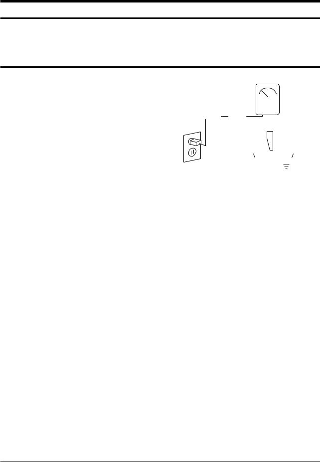
4.Leakage Current Hot Check (Figure 1-1): Warning: Do not use an isolation transformer during this test. Use a leakagecurrent tester or a metering system that complies with American National Standards Institute (ANIS C101.1, Leakage Current for Appliances), and Underwriters Laboratories (UL Publication UL1410, 59.7).
5.With the unit completely reassembled, plug the AC line cord directly into the power outlet. With the unit’s AC switch first in the ON position and then OFF, measure the current between a known earth ground (metal water pipe, conduit, etc.) and all exposed metal parts, including: antennas, handle brackets, metal cabinets, screwheads and control shafts. The current measured should not exceed 0.5 milliamp. Reverse the powerplug prongs in the AC outlet and repeat the test.
|
|
|
|
|
|
|
|
|
|
(READING SHOULD |
||
|
|
|
|
|
|
|
|
|
|
|||
|
|
|
|
|
|
|
|
|
|
|||
|
|
|
|
|
|
|
LEAKAGE |
NOT BE ABOVE |
||||
|
DEVICE |
|
|
|
|
|
CURRENT |
|
0.5mA) |
|||
|
UNDER |
|
|
|
|
|
TESTER |
|
|
|
||
|
TEST |
|
|
|
|
|
|
|
|
|
|
|
|
|
|
|
|
|
|
|
|||||
|
|
|
TEST ALL |
|
|
|
|
|
|
|
||
|
|
EXPOSED METAL |
|
|
|
|
|
|
|
|||
|
|
|
SURFACES |
|
|
|
|
|
|
|
||
|
2-WIRE CORD |
|
|
|
|
|
|
|
||||
|
ALSO TEST WITH |
|
|
|
|
|
|
|
||||
|
PLUG REVERSED |
|
|
|
|
|
|
|
|
|||
|
(USING AC ADAPTER |
|
|
|
|
|
|
|
EARTH |
|||
|
PLUG AS REQUIRED) |
|
|
|
|
|
GROUND |
|||||
|
|
|
|
|
|
|
|
|
|
|
|
|
Fig. 1-1 AC Leakage Test
6.Antenna Cold Check:
With the unit’s AC plug disconnected from the AC source, connect an electrical jumper across the two AC prongs. Connect one lead of the ohmmeter to an AC prong. Connect the other lead to the coaxial connector.
7.X-ray Limits:
The picture tube is especially designed to prohibit X-ray emissions. To ensure continued X-ray protection, replace the picture tube only with one that is the same type as the original. Carefully reinstall the picture tube shields and mounting hardware; these also provide X-ray protection.
8.High Voltage Limits:
High voltage must be measured each time servicing is done on the B+, horizontal deflection or high voltage circuits. Correct operation of the X-ray protection circuits must be
reconfirmed whenever they are serviced. (X-ray protection circuits also may be called “horizontal disable” or “hold-down”.)
Heed the high voltage limits. These include the X–ray Protection Specifications Label, and the Product Safety and X-ray Warning Note on the service data schematic.
Samsung Electronics |
1-1 |

Precautions
1-1 Safety Precautions (Continued)
9.High voltage is maintained within specified limits by close-tolerance, safety-related components and adjustments. If the high voltage exceeds the specified limits, check each of the special components.
10.Design Alteration Warning:
Never alter or add to the mechanical or electrical design of this unit. Example: Do not add auxiliary audio or video connectors. Such alterations might create a safety hazard. Also, any design changes or additions will void the manufacturer’s warranty.
11.Hot Chassis Warning:
Some TV receiver chassis are electrically connected directly to one conductor of the AC power cord. If an isolation transformer is not used, these units may be safely serviced only if the AC power plug is inserted so that the chassis is connected to the ground side of the AC source.
To confirm that the AC power plug is inserted correctly, do the following: Using an AC voltmeter, measure the voltage between the chassis and a known earth ground. If the reading is greater than 1.0V, remove the AC power plug, reverse its polarity and reinsert. Re-measure the voltage between the chassis and ground.
12.Some TV chassis are designed to operate with 85 volts AC between chassis and ground, regardless of the AC plug polarity. These units can be safely serviced only if an isolation transformer inserted between the receiver and the power source.
13.Some TV chassis have a secondary ground system in addition to the main chassis ground. This secondary ground system is not
isolated from the AC power line. The two ground systems are electrically separated by insulating material that must not be defeated or altered.
14.Components, parts and wiring that appear to have overheated or that are otherwise damaged should be replaced with parts that meet the original specifications. Always determine the cause of damage or overheating, and correct any potential hazards.
15.Observe the original lead dress, especially near the following areas: Antenna wiring, sharp edges, and especially the AC and high voltage power supplies. Always inspect for pinched, out-of-place, or frayed wiring. Do not change the spacing between components and the printed circuit board. Check the AC power cord for damage. Make sure that leads and components do not touch thermally hot parts.
16.Picture Tube Implosion Warning:
The picture tube in this receiver employs “integral implosion” protection. To ensure continued implosion protection, make sure that the replacement picture tube is the same as the original.
17.Do not remove, install or handle the picture tube without first putting on shatterproof goggles equipped with side shields. Never handle the picture tube by its neck. Some “in-line” picture tubes are equipped with a permanently attached deflection yoke; do not try to remove such “permanently attached” yokes from the picture tube.
18.Product Safety Notice:
Some electrical and mechanical parts have special safety-related characteristics which might not be obvious from visual inspection. These safety features and the protection they give might be lost if the replacement component differs from the original—even if the replacement is rated for higher voltage, wattage, etc.
Components that are critical for safety are
indicated in the circuit diagram by shading, (  ) or ( ! ).
Use replacement components that have the same ratings, especially for flame resistance and dielectric strength specifications.
A replacement part that does not have the same safety characteristics as the original might create shock, fire or other hazards.
1-2 |
Samsung Electronics |

Precautions
1-2 Servicing Precautions
Warning 1 : First read the “Safety Precautions” section of this manual. If some unforeseen circumstance creates a conflict between the servicing and safety precautions, always follow the safety precautions.
Warning 2 : An electrolytic capacitor installed with the wrong polarity might explode.
1.Servicing precautions are printed on the cabinet. Follow them.
2.Always unplug the unit’s AC power cord from the AC power source before attempting to: (a) Remove or reinstall any component or assembly, (b) Disconnect an electrical plug or connector, (c) Connect a test component in parallel with an electrolytic capacitor.
3.Some components are raised above the printed circuit board for safety. An insulation tube or tape is sometimes used. The internal wiring is sometimes clamped to prevent contact with thermally hot components. Reinstall all such elements to their original position.
4.After servicing, always check that the screws, components and wiring have been correctly reinstalled. Make sure that the portion around the serviced part has not been damaged.
5.Check the insulation between the blades of the AC plug and accessible conductive parts (examples: metal panels, input terminals and earphone jacks).
6.Insulation Checking Procedure: Disconnect the power cord from the AC source and turn the power switch ON. Connect an insulation resistance meter (500V) to the blades of the AC plug.
The insulation resistance between each blade of the AC plug and accessible conductive parts (see above) should be greater than 1 megohm.
7.Never defeat any of the B+ voltage interlocks. Do not apply AC power to the unit (or any of its assemblies) unless all solid-state heat sinks are correctly installed.
8.Always connect a test instrument’s ground lead to the instrument chassis ground before connecting the positive lead; always remove the instrument’s ground lead last.
Samsung Electronics |
1-3 |

Precautions
1-3 Precautions for Electrostatically Sensitive Devices (ESDs)
1.Some semiconductor (“solid state”) devices are easily damaged by static electricity. Such components are called Electrostatically Sensitive Devices (ESDs); examples include integrated circuits and some field-effect transistors. The following techniques will reduce the occurrence of component damage caused by static electricity.
2.Immediately before handling any semicon ductor components or assemblies, drain the electrostatic charge from your body by touching a known earth ground. Alternatively, wear a discharging wrist-strap device. (Be sure to remove it prior to applying power— this is an electric shock precaution.)
3.After removing an ESD-equipped assembly, place it on a conductive surface such as aluminum foil to prevent accumulation of electrostatic charge.
4.Do not use freon-propelled chemicals. These can generate electrical charges that damage ESDs.
5.Use only a grounded-tip soldering iron when soldering or unsoldering ESDs.
6.Use only an anti-static solder removal device. Many solder removal devices are not rated as “anti-static”; these can accumulate sufficient electrical charge to damage ESDs.
7.Do not remove a replacement ESD from its protective package until you are ready to install it. Most replacement ESDs are packaged with leads that are electrically shorted together by conductive foam, aluminum foil or other conductive materials.
8.Immediately before removing the protective material from the leads of a replacement ESD, touch the protective material to the chassis or circuit assembly into which the device will be installed.
9.Minimize body motions when handling unpackaged replacement ESDs. Motions such as brushing clothes together, or lifting a foot from a carpeted floor can generate enough static electricity to damage an ESD.
1-4 |
Samsung Electronics |

Specifications and IC Data
2. Specifications and IC Data
2-1 Specifications
|
|
|
CT-565BZ / 566BWZ |
|
|
CT-765DWZ |
MODEL |
CT-5072BWZ |
|
CT-567BWZ / 568BPZ |
CT-25D4WZ |
CT-29D4WZ |
CT-766DWZ |
CT-5072BPZ |
|
|||||
|
|
CT-225BZ / 228BWZ |
|
|
CT-30D6PZ |
|
|
|
|
CT-22B6PZ |
|
|
CT-30A9PZ |
VOLTAGE |
|
|
|
|
± |
|
|
|
|
AC100-240V (Mexico: AC127V 10%) |
|
||
POWER CONSUMPTION |
|
85 WATTS |
110 WATTS |
120 WATTS |
120 WATTS |
|
POWER FREQUENCY |
|
|
50/60Hz (Mexico: 60Hz) |
|
||
|
|
|
|
|
|
|
CHANNELS RECEIVED |
|
|
VHF; 2~13, UHF; 14~69, CATV; 1,14~125 |
|
||
MODEL |
TXJ2048/2060 |
TXJ2554/2566 |
TXJ2754/2766 |
TXJ2879 |
|
||||
|
TXJ2066/2067 |
TXJ2567 |
TXJ2767/2768 |
|
|
|
|||
|
|
|
|
|
VOLTAGE |
|
AC120V |
|
|
|
|
|
|
|
POWER CONSUMPTION |
85 WATTS |
110 WATTS |
120 WATTS |
130 WATTS |
|
|
|
|
|
POWER FREQUENCY |
|
60Hz |
|
|
|
|
|
|
|
CHANNELS RECEIVED |
VHF; 2~13, UHF; 14~69, CATV; 1,14~125 |
|||
|
|
|
|
|
|
CN-565BWZ |
|
CN-25D4WZ |
|
CN-29D4WZ |
MODEL |
|
|
CN-7202WZ |
||
CN-566BWZ |
|
CN-663AWZ |
|
||
|
|
|
CN-765DWZ |
||
|
|
|
|
|
|
|
|
|
|
||
VOLTAGE |
AC 100-240V (Argentina: AC 220V) |
||||
|
|
|
|
|
|
POWER CONSUMPTION |
85 WATTS |
|
110 WATTS |
|
120 WATTS |
|
|
|
|
|
|
POWER FREQUENCY |
|
50/60 Hz (Argentina: 50 Hz) |
|
||
|
|
|
|
||
CHANNELS RECEIVED |
VHF: 2~13, UHF: 14~69, CATV: 1,14~125 |
||||
|
|
|
|
|
|
Samsung Electronics |
2-1 |

Specifications and IC Data
2-2 IC Line Up
Table 2 - 1 IC Line - Up
|
|
|
|
|
|
|
|
|
|
|
|
|
|
|
|
Loc No |
|
|
No |
|
|
Specification |
|
|
Description |
|
|
Remarks |
|
|
|
|
|
|
|
|
|
|
|
|
|
|
|
|
|
SF101 |
|
|
1 |
|
|
M3951M |
|
|
SAW FILTER (VIF) |
|
|
|
|
|
|
|
|
|
|
|
|
|
|
|
|
|
|
|
|
SF102 |
|
|
2 |
|
|
M9260M |
|
|
SAW FILTER (SIF) |
|
|
|
|
|
|
|
|
|
|
|
|
|
|
|
|
|
|
|
|
|
|
|
|
|
|
TDA8377 |
|
|
ONECHIP TV PROCESSOR |
|
|
CT566BV/CT567BW/CT568BW/CT766DW |
|
|
IC201 |
|
|
|
|
|
|
|
|
|
|
|
|
|
|
|
|
3 |
|
|
TDA8373 |
|
|
ONECHIP TV PROCESSOR |
|
|
CT633BW/CT683BW |
|
|
|
|
|
|
|
|
|
|
|
|
|
|
|
|
|
|
|
|
|
|
|
|
TDA8375 |
|
|
ONECHIP TV PROCESSOR |
|
|
CN565BW/CN25D4W/CN663A/CN765DW |
|
|
|
|
|
|
|
|
|
|
|
|
|
|
|
|
|
IC202 |
|
|
4 |
|
|
LA7510 |
|
|
AUDIO IF AMP/4.5M DETECT |
|
|
|
|
|
|
|
|
|
|
|
|
|
|
|
|
|
|
|
|
IC301 |
|
|
5 |
|
|
LA7845 |
|
|
VERTICAL AMP IC |
|
|
|
|
|
|
|
|
|
|
|
|
|
|
|
|
|
|
|
|
|
|
|
|
|
|
TDA7056B |
|
|
|
|
|
1.5W x 2 (MONO) |
|
|
IC603 |
|
|
6 |
|
|
|
|
|
SOUND AMP IC |
|
|
|
|
|
|
|
|
|
|
|
|
|
|
3W x 2 (MONO) |
|
|||
|
|
|
|
|
|
|
TDA7266S |
|
|
|
|
|
|
|
|
|
|
|
|
|
|
|
|
|
|
|
STEREO MODEL |
|
|
|
|
|
|
|
|
|
|
|
|
|
|
|
|
|
|
|
|
|
|
|
|
|
|
|
|
|
|
|
|
|
IC701 |
|
|
7 |
|
|
TDA7449 |
|
|
VOLUME CONTROL IC |
|
|
|
|
|
|
|
|
|
|
|
|
|
|
|
|
|
|
|
|
IC801 |
|
|
8 |
|
|
KA3S1265R |
|
|
POWER IC |
|
|
CT633BW/CT683BW/CT766DW |
|
|
|
|
|
|
|
|
|
|
|
|
||||
|
|
|
|
|
|
|
|
|
CT566BV/CT566BW/CT567BW/CT568BW |
|
||||
|
|
|
|
|
|
|
|
|
|
|
|
|
|
|
|
|
|
|
|
|
|
|
|
|
|
|
|
|
|
|
IC802 |
|
|
9 |
|
|
KA7630 |
|
|
MULTI REGULATOR IC |
|
|
|
|
|
|
|
|
|
|
|
|
|
|
|
|
|
|
|
|
IC901 |
|
|
10 |
|
|
SZM368ET |
|
|
MICOM |
|
|
|
|
|
|
|
|
|
|
|
|
|
|
|
|
|
|
|
|
IC902 |
|
|
11 |
|
|
XL24C08P |
|
|
EEPROM |
|
|
|
|
|
|
|
|
|
|
|
|
|
|
|
|
|
|
|
|
ICD01 |
|
|
12 |
|
|
CXA2104S |
|
|
MTS IC |
|
|
STEREO MODEL ONLY |
|
|
|
|
|
|
|
|
|
|
|
|
|
|
|
|
|
|
|
|
|
|
|
|
|
|
|
|
|
|
|
|
|
|
|
|
|
|
|
|
|
|
|
|
|
|
2-2 |
Samsung Electronics |
Specifications and IC Data
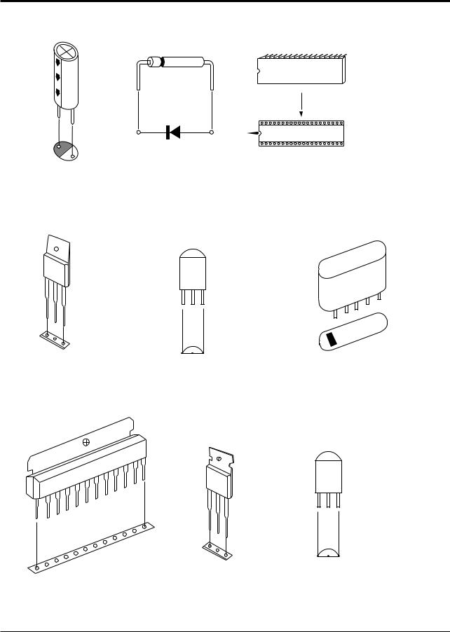
2-3 Semiconductor Base Diagrams
ELECTROLYTIC-
CONDENSER
DIODE |
IC |
XLS24C08P (PIN 8)
TDA8377 (PIN 56)
TRANSISTOR |
TRANSISTOR |
|
SAW-FILTER |
|
KSC2073 |
|
M3951M |
|
KSA940 |
|
M9260M |
|
2SD1887 |
KSC815Y |
|
|
2SD1880 |
|
|
|
KSA539-Y |
1 |
|
|
KSD5072 |
||
|
|
||
|
KSD5703 |
|
|
B
C
E
E B C
IC |
TRANSISTOR |
TRANSISTOR |
|
LA7845
C2331-Y
KSR1010
KA7812
KA7809
IN
G |
E C B |
out |
Fig. 2-1 Semiconductor Base Diagrams
Samsung Electronics |
2-3 |

Specifications and IC Data
2-4 One Chip TV-processor
|
|
|
|
|
|
|
|
|
|
|
|
|
|
SOUND IF INPUT |
|
|
1 |
|
56 |
DECOUPLING SOUND DEMODULATOR |
|||||||
EXT AUDIO INPUT |
|
|
|
|
|
|
|
|
|
|
|
|
|
|
|
|
|
|
|
|
|
|
2 |
|
55 |
AUDIO DEEMPHASSIS/MPX OUT |
|
VCO REF FILTER |
|
|
|
|
|
|
|
|
|
|
|
|
|
|
|
|
|
|
|
|
|
3 |
|
54 |
TUNER AGC OUTPUT |
||
VCO REF FILTER |
|
|
|
|
|
|
|
|
|
|
|
|
AGC DECOUPLING CAPACITOR |
|
|
|
|
|
|
|
|
|
4 |
|
53 |
||
PLL LOOP FILTER |
|
|
|
|
|
|
|
|
|
|
|
REREFERENCE CURRENT INPUT |
|
|
|
|
|
|
|
|
|
|
5 |
|
52 |
||
IF VIDEO OUTPUT |
|
|
|
|
|
|
|
|
|
|
|
|
|
|
|
|
|
|
|
|
6 |
|
51 |
VERT, SAWTOOTH CAPACITOR |
|||
|
|
|
|
|
|
|
|
|
|
|
|
|
EHT/OVERVOLTAGE PROTECTION INP |
BUSINPUT : SCL |
|
|
|
|
|
|
|
|
|
7 |
|
50 |
|
|
|
|
|
|
|
|
|
|
(X-RAY PROTECTION) |
||||
BUSINPUT : SDA |
|
|
|
|
|
|
|
|
|
|
|
|
|
|
|
|
|
|
|
|
|
|
|
|
|
||
|
|
8 |
|
49 |
IF INPUT |
||||||||
BANDGAP DECOUPLING |
|
|
|
|
|
|
|
|
|
|
IF INPUT |
||
|
|
|
|
|
|
|
|
|
9 |
|
48 |
||
CHROMA INPUT |
|
|
|
|
|
|
|
|
|
|
|
|
|
|
|
|
|
|
|
|
|
|
10 |
|
47 |
VERT. DRIVE NEG |
|
Y/CVBS INPUT |
|
|
|
|
|
|
|
|
|
|
|||
|
|
|
|
|
|
|
|
|
11 |
|
46 |
VERT. DRIVE POS |
|
MAIN POSITIVE SUPPLY |
|
|
|
|
|
|
|
|
|
|
|
|
EAST-WEST DRIVE |
|
|
|
|
|
|
|
|
|
12 |
|
45 |
||
INT CVBS INPUT |
|
|
|
|
|
|
|
|
|
||||
|
|
|
|
|
|
|
|
|
13 |
|
44 |
GROUND |
|
GROUND |
|
|
|
|
|
|
|
|
|
|
|
|
|
|
|
|
|
|
|
|
|
|
14 |
|
43 |
PHI1 FILTER |
|
AUDIO OUT |
|
|
|
|
|
|
|
||||||
|
|
|
|
|
|
|
|
|
15 |
|
42 |
PHI2 FILTER / FLASH PROT |
|
DECOUPLING FILTER TUNING |
|
|
|
|
|
|
|
|
|
|
|
|
|
|
|
|
|
16 |
|
41 |
SAND CASTLE OUTPUT/FLYBACK INP |
||||||
EXT CVBS INPUT |
|
|
|
|
|
|
|
|
|
|
|
|
|
|
|
|
17 |
|
40 |
HOR. OUTPUT |
|||||||
BLACK CURRENT INP |
|
|
|
|
|
|
|
|
|
|
|
|
|
|
|
|
|
|
|
|
|
|
18 |
|
39 |
BLACK PEAK HOLD CAPACITOR |
|
|
|
|
|
|
|
|
|
|
|
|
|
|
|
BLUE OUTPUT |
|
|
|
|
|
|
|
|
|
19 |
|
38 |
CVBS OUTPUT |
GREEN OUTPUT |
|
|
|
|
|
|
|
|
|
|
|
|
|
|
|
|
|
|
|
|
|
|
20 |
|
37 |
POSITIVE SUPPLY |
|
|
|
|
|
|
|
|
|
|
|
|
|
|
|
RED OUTPUT |
|
|
|
|
|
|
|
|
|
21 |
|
36 |
LOOP FILTER BURST PHASE DET |
V-GUARD INP/BEAM CUR LIMITER |
|
|
|
|
|
|
|
|
|
|
|
|
|
|
|
|
|
|
|
|
|
|
22 |
|
35 |
X-TAL (PAL-N (4.43)/PAL-M (3.58)) |
|
RED INPUT |
|
|
|
|
|
|
|
|
|
|
|
|
X-TAL (3.58) |
|
|
|
|
|
|
|
|
|
23 |
|
34 |
||
GREEN INPUT |
|
|
|
|
|
|
|
|
|
|
|
SECAM REF OUTPUT |
|
|
|
|
|
|
|
|
|
|
24 |
|
33 |
||
|
|
|
|
|
|
|
|
|
|
|
|
|
|
BLUE INPUT |
|
|
|
|
|
|
25 |
|
32 |
(R-Y) INPUT |
|||
|
|
|
|
|
|
|
|
|
|
|
|
|
(B-Y) INPUT |
PIP/OSD RGB INSERTION SWITCH INP |
|
26 |
|
31 |
|||||||||
|
|
|
|
|
|
|
|
|
|
|
|
|
|
LUMINANCE INPUT |
|
|
|
|
|
27 |
|
30 |
(R-Y) OUTPUT |
||||
|
|
|
|
|
|
|
|
|
|
|
SDIL56 |
|
|
LUMINANCE OUTPUT |
28 |
29 |
(B-Y) OUTPUT |
||||||||||
|
|
|
|
|
|
|
|
|
|
|
|
|
|
Fig. 2-2 SDIL56
CVBS : Composite Video Blanking Signal
2-4 |
Samsung Electronics |
Alignment and Adjustments
3. Alignment and Adjustments
3-1 Preadjustment
1.Since there are no VRs in the K51A chassis, all adjustments after parts replacement must be done in the Service Mode.
2.The Factory Mode adjustments are necessary when either the EEPROM (IC902) or the CRT is replaced.
3.Do not tamper with the “ Adjustment” screen of the Factory Mode menu. This screen is intended only for factory use.
4. WHEN EEPROM (IC902) IS REPLACED
(1)When IC902 is replaced, all adjustment data revert to their initial values. It is necessary to re-program this data.
(2)After IC902 is replaced, warm up the TV for 10 seconds.
Make the following adjustments AFTER setting up purity and convergence:
White Balance Sub-Brightness Vertical Center Vertical Size
Horizontal Size (No use in 21” and 25” models)
3-2 Factory (“SERVICE”) Mode
1.The set must be in Factory (“Service”) Mode. Selection sequence:
STAND-BY → MUTE → 1 →8 → 2 → POWER ON
2.The “ FACTORY MODE” message will be displayed. The Factory Mode has four components : Adjustment, MPX, PIP, Option Byte and Factory Reset.
3. Access the Adjustment Mode by pressing the “VOLUME” keys (▼, The adjustment parameters are listed in the accompanying table. Select them by pressing the CHANNEL keys (▲,▼).
▼)
4.After completing the Factory Mode adjustments, turn the power switch OFF.
Samsung Electronics |
3-1 |
Alignment and Adjustments
3-2-1 Adjustment
1.Selection sequence :
STAND-BY → MUTE → 1 → 8 → 2 → POWER ON
2.Example : Sub-bright Adjustment
SZM368ET1 (R4027)
*FACTORY*
Adjustment
Mpx
Pattern
Option
Reset
↓ Press VOL ▼
AGC |
15 |
|
V S |
3 2 |
VCO |
62 |
|
V A |
2 7 |
S B T |
7 |
|
H S |
4 6 |
SCT |
11 |
|
EWA |
52 |
S C R |
8 |
|
EWP |
31 |
S T T |
8 |
|
EWC |
32 |
R G |
3 2 |
|
EWT |
31 |
G G |
3 2 |
|
MAT |
off |
B G |
3 2 |
|
P L A |
6 |
SCO |
20 |
|
|
|
VSL |
26 |
|
|
|
|
|
↓ |
Press CH ▼ |
|
AGC |
15 |
|
V S |
3 2 |
VCO |
62 |
|
V A |
2 7 |
S B T |
7 |
|
H S |
4 6 |
SCT |
11 |
|
EWA |
52 |
S C R |
8 |
|
EWP |
31 |
S T T |
8 |
|
EWC |
32 |
R G |
3 2 |
|
EWT |
31 |
G G |
3 2 |
|
MAT |
off |
B G |
3 2 |
|
P L A |
6 |
SCO |
20 |
|
|
|
VSL |
26 |
|
|
|
↓ Press VOL ▼ or ▼
SBT 3
↓
POWER OFF
SZM368ET2 (R4127)
*SERVICE*
Adjustment
MTS
PIP
Option
Reset
↓ Press VOL ▼
|
|
|
|
|
|
|
|
|
AGC |
15 |
|
|
VSLN |
30 |
VSLP |
30 |
|
VCO |
62 |
|
|
VSN |
32 |
VSP |
32 |
|
S B T |
7 |
|
|
VAN |
32 |
VAP |
32 |
|
SCT |
11 |
|
|
HSN |
45 |
HSP |
39 |
|
S C R |
8 |
|
|
EWAN |
45 |
EWAP |
46 |
|
S T T |
8 |
|
|
EWPN |
33 |
EWPP |
33 |
|
R G |
3 2 |
|
|
EWCN |
32 |
EWCP |
32 |
|
G G |
3 2 |
|
|
EWTN |
38 |
EWPT |
38 |
|
B G |
3 2 |
|
|
|
|
|
|
|
SCO |
20 |
|
|
|
|
|
|
|
P L A |
5 |
|
|
|
|
|
|
|
|
|
|
↓ |
|
Press CH ▼ |
|
|
|
AGC |
15 |
|
|
VSLN |
30 |
VSLP |
30 |
|
VCO |
62 |
|
|
VSN |
32 |
VSP |
32 |
|
S B T |
7 |
|
|
VAN |
32 |
VAP |
32 |
|
SCT |
11 |
|
|
HSN |
45 |
HSP |
39 |
|
S C R |
8 |
|
|
EWAN |
45 |
EWAP |
46 |
|
S T T |
8 |
|
|
EWPN |
33 |
EWPP |
33 |
|
R G |
3 2 |
|
|
EWCN |
32 |
EWCP |
32 |
|
G G |
3 2 |
|
|
EWTN |
38 |
EWPT |
38 |
|
B G |
3 2 |
|
|
|
|
|
|
|
SCO |
20 |
|
|
|
|
|
|
|
P L A |
5 |
|
|
|
|
|
|
|
↓ Press VOL ▼ or ▼
SBT 3
↓
POWER OFF
3-2 |
Samsung Electronics |

Alignment and Adjustments
MEMORY SPECIFICATION
Table 3 - 1 Memory Specification
|
|
|
|
|
|
|
|
|
|
|
|
|
|
|
|
|
|
|
|
|
|
|
|
|
|
|
|
|
|
|
|
|
|
|
|
|
|
|
FUNCTION |
|
|
No |
|
|
|
MODE |
|
|
|
RANGE |
|
|
28B2 |
|
|
|
|
|
|
|
|
228BWX |
|
|
|
|
|
565BZ |
|
|
566BWZ |
|
|
765DWZ |
|
|
|
|
|
|
|
29D4WZ |
|
|
225BZ |
25D4WZ |
|
||||||||||||||||||||||||||
|
|
|
|
|
|
|
|
(OSD) |
|
|
|
|
|
|
|
|
|
|
|
|
|
|
|
|
|
|
|
|
|
|
|
|
|
|
|
|
|
|
|
|
|
|
|
|
|
|
|
|
|
|
|
|
|
|
|
|
|
|
|
|
|
|
|
|
|
|
|
|
|
|
|
|
|
|
|
|
|
|
|
1 |
|
|
|
AGC |
|
|
|
63 |
|
|
8 |
|
|
8 |
|
|
8 |
|
|
8 |
|
|
8 |
|
|
8 |
|
|
8 |
|
|
8 |
|
|
|
|
|
|
|
|
|
|
|
|
|
|
|
|
|
|
|
|
|
|
|
|
|
|
|
|
|
|
|
|
|
|
|
|
|
|
|
|
|
|
|
2 |
|
|
|
VCO |
|
|
|
127 |
|
|
63 |
|
|
63 |
|
|
63 |
|
|
63 |
|
|
63 |
|
|
63 |
|
|
63 |
|
|
63 |
|
|
|
|
|
|
|
|
|
|
|
|
|
|
|
|
|
|
|
|
|
|
|
|
|
|
|
|
|
|
|
|
|
|
|
|
|
|
|
|
|
|
|
3 |
|
|
|
SBT |
|
|
|
15 |
|
|
2 |
|
|
2 |
|
|
2 |
|
|
2 |
|
|
2 |
|
|
2 |
|
|
2 |
|
|
2 |
|
|
|
|
|
|
|
|
|
|
|
|
|
|
|
|
|
|
|
|
|
|
|
|
|
|
|
|
|
|
|
|
|
|
|
|
|
|
|
|
|
|
|
4 |
|
|
|
SCT |
|
|
|
13 |
|
|
7 |
|
|
7 |
|
|
7 |
|
|
7 |
|
|
7 |
|
|
7 |
|
|
7 |
|
|
7 |
|
|
A |
|
|
5 |
|
|
|
SCR |
|
|
|
13 |
|
|
0 |
|
|
0 |
|
|
0 |
|
|
0 |
|
|
0 |
|
|
0 |
|
|
0 |
|
|
0 |
|
|
D |
|
|
6 |
|
|
|
STT |
|
|
|
13 |
|
|
4 |
|
|
4 |
|
|
4 |
|
|
4 |
|
|
4 |
|
|
4 |
|
|
4 |
|
|
7 |
|
|
J |
|
|
7 |
|
|
|
RG |
|
|
|
63 |
|
|
32 |
|
|
32 |
|
|
20 |
|
|
20 |
|
|
32 |
|
|
20 |
|
|
20 |
|
|
32 |
|
|
|
|
|
|
|
|
|
|
|
|
|
|
|
|
|
|
|
|
|
|
|
|
|
|
|
|
|
|
|
|
|
|
|
|
|
|
|
|
U |
|
|
8 |
|
|
|
GG |
|
|
|
63 |
|
|
32 |
|
|
32 |
|
|
20 |
|
|
20 |
|
|
32 |
|
|
20 |
|
|
20 |
|
|
32 |
|
|
|
|
|
|
|
|
|
|
|
|
|
|
|
|
|
|
|
|
|
|
|
|
|
|
|
|
|
|
|
|
|
|
|
|
|
|
|
|
S |
|
|
9 |
|
|
|
BG |
|
|
|
63 |
|
|
32 |
|
|
32 |
|
|
20 |
|
|
20 |
|
|
32 |
|
|
20 |
|
|
20 |
|
|
32 |
|
|
|
|
|
|
|
|
|
|
|
|
|
|
|
|
|
|
|
|
|
|
|
|
|
|
|
|
|
|
|
|
|
|
|
|
|
|
|
|
T |
|
|
10 |
|
|
|
SCO |
|
|
|
63 |
|
|
20 |
|
|
14 |
|
|
14 |
|
|
14 |
|
|
14 |
|
|
14 |
|
|
14 |
|
|
14 |
|
|
|
|
|
|
|
|
|
|
|
|
|
|
|
|
|
|
|
|
|
|
|
|
|
|
|
|
|
|
|
|
|
|
|
|
|
|
|
|
M |
|
|
11 |
|
|
|
VSL |
|
|
|
63 |
|
|
28 |
|
|
26 |
|
|
24 |
|
|
24 |
|
|
23 |
|
|
24 |
|
|
24 |
|
|
25 |
|
|
|
|
|
|
|
|
|
|
|
|
|
|
|
|
|
|
|
|
|
|
|
|
|
|
|
|
|
|
|
|
|
|
|
|
|
|
|
|
E |
|
|
12 |
|
|
|
VS |
|
|
|
63 |
|
|
20 |
|
|
32 |
|
|
32 |
|
|
32 |
|
|
32 |
|
|
32 |
|
|
32 |
|
|
26 |
|
|
|
|
|
|
|
|
|
|
|
|
|
|
|
|
|
|
|
|
|
|
|
|
|
|
|
|
|
|
|
|
|
|
|
|
|
|
|
|
N |
|
|
13 |
|
|
|
VA |
|
|
|
63 |
|
|
38 |
|
|
29 |
|
|
36 |
|
|
36 |
|
|
27 |
|
|
36 |
|
|
36 |
|
|
34 |
|
|
T |
|
|
14 |
|
|
|
HS |
|
|
|
63 |
|
|
44 |
|
|
48 |
|
|
46 |
|
|
46 |
|
|
41 |
|
|
46 |
|
|
46 |
|
|
46 |
|
|
|
|
|
|
|
|
|
|
|
|
|
|
|
|
|
|
|
|
|
|
|
|
|
|
|
|
|
|
|
|
|
|
|
|
|
|
|
|
|
|
|
15 |
|
|
|
EWA |
|
|
|
63 |
|
|
42 |
|
|
33 |
|
|
47 |
|
|
47 |
|
|
32 |
|
|
47 |
|
|
47 |
|
|
51 |
|
|
|
|
|
|
|
|
|
|
|
|
|
|
|
|
|
|
|
|
|
|
|
|
|
|
|
|
|
|
|
|
|
|
|
|
|
|
|
|
|
|
|
16 |
|
|
|
EWP |
|
|
|
63 |
|
|
45 |
|
|
34 |
|
|
4 |
|
|
4 |
|
|
36 |
|
|
4 |
|
|
4 |
|
|
24 |
|
|
|
|
|
|
|
|
|
|
|
|
|
|
|
|
|
|
|
|
|
|
|
|
|
|
|
|
|
|
|
|
|
|
|
|
|
|
|
|
|
|
|
17 |
|
|
|
EWC |
|
|
|
63 |
|
|
32 |
|
|
32 |
|
|
32 |
|
|
32 |
|
|
32 |
|
|
32 |
|
|
32 |
|
|
32 |
|
|
|
|
|
|
|
|
|
|
|
|
|
|
|
|
|
|
|
|
|
|
|
|
|
|
|
|
|
|
|
|
|
|
|
|
|
|
|
|
|
|
|
18 |
|
|
|
EWT |
|
|
|
63 |
|
|
32 |
|
|
32 |
|
|
32 |
|
|
32 |
|
|
32 |
|
|
32 |
|
|
32 |
|
|
32 |
|
|
|
|
|
|
|
|
|
|
|
|
|
|
|
|
|
|
|
|
|
|
|
|
|
|
|
|
|
|
|
|
|
|
|
|
|
|
|
|
|
|
|
19 |
|
|
|
PLA |
|
|
|
10 |
|
|
5 |
|
|
0 |
|
|
6 |
|
|
6 |
|
|
0 |
|
|
6 |
|
|
6 |
|
|
5 |
|
|
|
|
|
|
|
|
|
|
|
|
|
|
|
|
|
|
|
|
|
|
|
|
|
|
|
|
|
|
|
|
|
|
|
|
|
|
|
|
|
|
|
20 |
|
|
|
SEP |
|
|
|
31 |
|
|
OFF |
|
|
OFF |
|
|
OFF |
|
|
OFF |
|
|
OFF |
|
|
OFF |
|
|
OFF |
|
|
OFF |
|
|
|
|
|
|
|
|
|
|
|
|
|
|
|
|
|
|
|
|
|
|
|
|
|
|
|
|
|
|
|
|
|
|
|
|
|
|
|
|
|
|
|
|
|
|
|
|
|
|
|
|
|
|
|
|
|
|
|
|
|
|
|
|
|
|
|
|
|
|
|
|
|
|
|
|
|
|
OP |
|
|
|
|
|
BYTE 0 |
|
|
|
FF |
|
|
8F |
|
|
95 |
|
|
82 |
|
|
87 |
|
|
85 |
|
|
82 |
|
|
87 |
|
|
87 |
|
|
|
|
|
|
|
|
|
|
|
|
|
|
|
|
|
|
|
|
|
|
|
|
|
|
|
|
|
|
|
|
|
|
|
|
|
|
|
|
|
|
|
|
|
|
BYTE 1 |
|
|
|
FF |
|
|
03 |
|
|
00 |
|
|
00 |
|
|
00 |
|
|
00 |
|
|
00 |
|
|
00 |
|
|
00 |
|
||
|
|
|
|
|
|
|
|
|
|
|
|
|
|
|
|
|
|
|
|
|
|
|
|
|
|
|
|||||||||||
|
|
|
|
|
|
|
|
|
|
|
|
|
|
|
|
|
|
|
|
|
|
|
|
|
|
|
|
|
|
|
|
|
|
|
|
|
|
|
M |
|
|
|
|
|
|
ATT |
|
|
|
15 |
|
|
13 |
|
|
13 |
|
|
OFF |
|
|
13 |
|
|
13 |
|
|
OFF |
|
|
13 |
|
|
13 |
|
|
|
|
|
|
|
|
|
|
|
|
|
|
|
|
|
|
|
|
|
|
|
|
|
|
|
|
|
|
|
|
|
|
|
|
|
|
|
|
P |
|
|
|
|
SPECTRAL |
|
|
|
63 |
|
|
46 |
|
|
46 |
|
|
OFF |
|
|
46 |
|
|
46 |
|
|
OFF |
|
|
46 |
|
|
46 |
|
||
|
X |
|
|
|
|
|
|
|
|
|
|
|
|
|
|
|
|
|
|
|
|
|
|
|
|
|
|
|
|
|
|
|
|
|
|
|
|
|
|
|
|
WIDEBAND |
|
|
|
63 |
|
|
32 |
|
|
32 |
|
|
OFF |
|
|
32 |
|
|
32 |
|
|
OFF |
|
|
32 |
|
|
32 |
|
||||
|
|
|
|
|
|
|
|
|
|
|
|
|
|
|
|
|
|
|
|
|
|
|
|
|
|||||||||||||
|
|
|
|
|
|
|
|
|
|
|
|
|
|
|
|
|
|
|
|
|
|
|
|
|
|
|
|
|
|
|
|
|
|
|
|
|
|
|
|
|
|
|
|
|
|
|
|
|
|
x |
|
|
275 |
|
|
275 |
|
|
275 |
|
|
268 |
|
|
268 |
|
|
275 |
|
|
275 |
|
|
275 |
|
|
|
|
|
|
|
|
|
|
|
||||||||||||||||||||||||||||
|
|
|
|
|
|
|
|
|
|
|
|
|
|
|
|
|
|
|
|
|
|
|
|
|
|
|
|
|
|
|
|
|
|
|
|
||
|
|
|
|
|
HIGH - LIGHT |
|
|
|
y |
|
|
295 |
|
|
295 |
|
|
295 |
|
|
275 |
|
|
275 |
|
|
295 |
|
|
295 |
|
|
295 |
|
|||
|
WHITE |
|
|
|
|
|
|
|
|
|
Y ± 5 |
|
|
33 |
|
|
40 |
|
|
45 |
|
|
45 |
|
|
40 |
|
|
45 |
|
|
45 |
|
|
35 |
|
|
|
BALANCE |
|
|
|
|
|
|
|
|
|
|
|
|
|
|
|
|
|
|
|
|
|
|
|
|
|
|
|
|
|
|
|
|
|
|
|
|
|
|
|
LOW - LIGHT |
|
|
|
x |
|
|
275 |
|
|
275 |
|
|
275 |
|
|
277 |
|
|
277 |
|
|
275 |
|
|
275 |
|
|
275 |
|
|||||
ADJUSTMENT |
|
|
|
|
|
|
|
|
|
|
|
|
|
|
|
|
|
|
|
|
|
|
|||||||||||||||
|
|
|
|
|
|
|
|
|
|
|
|
|
|
|
|
|
|
|
|
|
|
|
|
|
|
|
|
|
|
|
|
|
|
|
|
|
|
|
|
|
|
|
|
|
|
|
|
|
|
y |
|
|
295 |
|
|
295 |
|
|
295 |
|
|
283 |
|
|
283 |
|
|
295 |
|
|
295 |
|
|
295 |
|
|
|
|
|
|
|
|
|
|
|
|
|
|
|
|
|
|
|
|
|
|
|
|
|
|
|
|
|
|
|
|
|
|
|
|
|
|
|
|
|
|
|
|
|
|
|
|
|
|
|
Y ± 0.2 |
|
|
1.4 |
|
|
1.4 |
|
|
1.4 |
|
|
1.4 |
|
|
1.4 |
|
|
1.4 |
|
|
1.4 |
|
|
1.4 |
|
|
|
|
|
|
|
|
|
|
|
|
|
|
|
|
|
|
|
|
|
|
|
|
|
|
|
|
|
|
|
||||||||
|
MEASURING PULS ADJUSTMENT VOLTAGE |
|
|
2.4V |
|
|
2.4V |
|
|
2.4V |
|
|
2.4V |
|
|
2.4V |
|
|
2.4V |
|
|
2.4V |
|
|
2.4V |
|
|||||||||||
|
|
|
|
|
|
|
|
|
|
|
|
|
|
|
|
|
|
|
|
|
|
|
|
|
|
|
|
|
|
|
|
|
|
|
|
|
|
|
|
|
|
|
|
|
|
|
|
|
|
|
|
|
|
|
|
|
|
|
|
|
|
|
|
|
|
|
|
|
|
|
|
|
|
|
|
|
|
|
|
|
|
|
|
|
|
|
|
|
|
|
|
|
|
|
|
|
|
|
|
|
|
|
|
|
|
|
|
|
|
|
|
|
|
|
|
|
|
|
|
|
|
|
|
|
|
|
|
|
|
|
|
|
|
|
|
|
|
|
|
|
|
|
|
|
|
|
|
|
|
|
|
Samsung Electronics |
3-3 |

Alignment and Adjustments
3-2-2 Option Table
NOTE : The Option Adjustment must be done in the Service Mode.
3-2-2 (A) OPTION BYTE 00
Table 3-2 Option Byte 00
|
|
|
|
|
|
|
|
|
|
|
|
|
|
|
|
|
|
|
|
|
|
|
|
FUNCTION |
|
|
|
|
|
|
BYTE : 00 |
|
|
NAME |
|
|
|
|
REMARK |
|||||
|
|
|
|
|
|
|
|
|
|
|
|
|
||
|
|
|
|
|
|
0 |
|
1 |
|
|
|
|
||
|
|
|
|
|
|
|
|
|
|
|
|
|||
|
|
|
|
|
|
|
|
|
|
|
|
|
|
|
|
|
|
|
|
|
|
|
|
|
|
|
|
|
|
|
D7 |
|
|
V-SYNC |
|
|
|
|
|
|
|
|
|
|
|
|
|
NOT USED |
|
USED ( NO V-SYNC, POWER OFF) |
|
|
|
|
|||||
|
|
|
|
|
|
|
|
|
|
|
|
|
|
|
|
D6 |
|
|
AUTO ON |
|
|
|
NOT USED |
|
USED |
|
|
|
|
|
|
|
|
|
|
|
|
|
|
|
|
|
|
|
|
D5 |
|
|
PIP |
|
|
|
NO PIP FUNCTION |
|
PIP FUNCTION |
|
|
|
|
|
|
|
|
|
|
|
|
|
|
|
|
|
|
|
|
D4 |
|
|
CATV |
|
|
|
AIR/STD/HRC/IRC |
|
AIR/STD/HRC/AFN |
|
|
ARMY : 1 |
|
|
|
|
|
|
|
|
|
|
|
|
|
|
|
|
|
D3 |
|
|
S-VIDEO |
|
|
|
NOT USED |
|
USED |
|
|
|
|
|
|
|
|
|
|
|
|
|
|
|
|
|
|
|
|
D2 |
|
|
TONE |
|
|
|
NO TONE CONTROL |
|
TONE CONTROL |
|
|
|
|
|
|
|
|
|
|
|
|
|
|
|
|
|
|
|
|
D1 |
|
|
CRT |
|
|
|
4 : 3 CRT |
|
12.8 : 9 CRT |
|
|
|
|
|
|
|
|
|
|
|
|
|
|
|
|
|
|
|
|
D0 |
|
|
MPX |
|
|
|
NOT USED |
|
USED |
|
|
|
|
|
|
|
|
|
|
|
|
|
|
|
|
|
|
|
|
|
|
|
|
|
|
|
|
|
|
|
|
|
|
|
|
|
|
|
|
|
|
|
|
|
|
|
|
|
3-2-2 (B) OPTION BYTE 01
Table 3-3 Option Byte 01
|
|
|
|
|
|
|
|
|
|
|
|
|
|
|
|
|
|
|
|
|
|
|
|
|
|
|
|
FUNCTION |
|
|
|
|
|
|
|
||||
|
BYTE : 01 |
|
|
NAME |
|
|
|
|
|
|
|
|
REMARK |
||||||
|
|
|
|
|
|
|
|
|
|
|
|
|
|
|
|
|
|
||
|
|
|
|
|
|
0 |
|
|
|
|
1 |
|
|
|
|
|
|
||
|
|
|
|
|
|
|
|
|
|
|
|
|
|
|
|
|
|
||
|
|
|
|
|
|
|
|
|
|
|
|
|
|
|
|
|
|
|
|
|
|
|
|
|
|
|
|
|
|
|
|
|
|
|
|
|
|
|
|
|
D7 |
|
|
|
|
|
|
|
|
|
|
|
|
|
|
|
|
|
|
|
|
|
|
|
|
|
|
|
|
|
|
|
|
|
|
||||
|
|
|
|
|
|
|
|
|
|
|
|
|
|
|
|
|
|
||
|
D6 |
|
|
AREA |
|
|
|
USA |
|
|
|
|
PAL M/N |
|
|
|
SYSTEM/LANGUAGE |
|
|
|
|
|
|
|
|
|
|
|
|
|
|
|
|
|
|
|
|
||
|
|
|
|
|
|
|
|
|
|
|
|
|
|
|
|
|
|||
|
|
|
|
|
|
|
|
|
|
|
|
|
|
|
|||||
|
|
|
|
|
|
|
|
|
|
|
|
|
|
||||||
|
D5 |
|
|
|
|
|
|
00 : ENGLISH |
|
|
|
|
|
||||||
|
|
|
|
|
|
|
01 : SPANISH (SEDA) |
|
|
|
|
|
|||||||
|
|
|
|
LANGUAGE |
|
|
|
|
|
|
PAL |
|
|||||||
|
|
|
|
|
|
02 : PORTUGUESE |
|
|
|
|
|||||||||
|
D4 |
|
|
|
|
|
|
|
|
|
|||||||||
|
|
|
|
|
|
|
|
|
|
|
|
||||||||
|
|
|
|
|
|
|
11 : NOT USED |
|
|
|
|
|
|||||||
|
|
|
|
|
|
|
|
|
|
|
|
|
|||||||
|
|
|
|
|
|
|
|
|
|
|
|
|
|
|
|
|
|
|
|
|
|
|
|
|
|
|
|
|
|
|
|
|
|
|
|
|
|
|
|
|
D3 |
|
|
NO VIDEO MUTE |
|
|
|
|
|
|
|
|
|
|
|
|
PAL |
|
|
VIDEO MUTE |
|
|
|
NO VIDEO MUTE |
|||||||||||||||
|
|
|
|
|
|
|
|
|
|
|
|
|
|
|
|
|
|||
|
D2 |
|
|
NO AUDIO MUTE |
|
|
|
AUDIO MUTE |
|
|
|
NO AUDIO MUTE |
|
|
|
|
|
||
|
|
|
|
|
|
|
|
|
|
|
|
|
|
|
|
|
|||
|
D1 |
|
|
ATS |
|
|
|
NO ATS |
|
|
|
ATS |
|
|
|
NT |
|
||
|
|
|
|
|
|
|
|
|
|
|
|
|
|
|
|
|
|||
|
D0 |
|
|
V-CHIP |
|
|
|
NO V - CHIP |
|
|
|
V-CHIP |
|
|
|
NT |
|
||
|
|
|
|
|
|
|
|
|
|
|
|
|
|
|
|
|
|
|
|
|
|
|
|
|
|
|
|
|
|
|
|
|
|
|
|
|
|
|
|
|
|
|
|
|
|
|
|
|
|
|
|
|
|
|
|
|
|
|
|
3-4 |
Samsung Electronics |
Alignment and Adjustments
3-2-4 Factory Reset
When “ Factory Reset” is selected, the User-Control data reverts to the initial values. The User-Control data is available at MENU (picture, sound and the other functions).
Note : When “ Factory Reset” is selected, the Factory Mode Data does not change.
Selection sequence :
Stand-By → MUTE → 1 → 8 → 2 → POWER ON
SZM368ET1 (R4027) |
|
SZM368ET2 (R4127) |
|
|
|
|
|
|
↓
* FACTORY *
Adjustment
Mpx
Pattern
Option
Reset
↓ Press CH ▼
Adjustment
Mpx
Pattern
Option
Reset
↓ Press VOL ▼
Execute
↓
* SERVICE *
Adjustment
MTS
PIP
Option
Reset
↓ Press CH ▼
Adjustment
MTS
PIP
Option
Reset
↓ Press VOL ▼
Execute
3-3 Other Adjustments
3-3-1 General
1.Usually, a color TV needs only slight touch-up adjustment upon installation. Check the basic characteristics such as height, horizontal and vertical sync and focus.
2.Observe the picture for good black and white details. There should be no objectionable color shading. If color shading is present, perform the purity and convergence adjustments described below.
3.Use the specified test equipment or its equivalent.
4.Correct impedance matching is essential.
5.Avoid overload. Excessive signal from a sweep generator might overload the front-end of the TV. When inserting signal markers, do not allow the marker generator to distort test results.
6.Connect the TV only to an AC power source with voltage and frequency as specified on the backcover nameplate.
7.Do not attempt to connect or disconnect any wires while the TV is turned on. Make sure that the power cord is disconnected before replacing any parts.
8.To protect against shock hazard, use an isolation transformer.
Samsung Electronics |
3-5 |
Alignment and Adjustments
3-3-2 Automatic Degaussing
A degaussing coil is mounted around the picture tube, so external degaussing after moving the TV should be unnecessary.
However, the receiver must be properly degaussed upon installation.
The degaussing coil operates for about 1 second after the power is switched ON. If the set has been moved or turned in a different direction, disconnect its AC power for at least 10 Minutes.
If the chassis or parts of the cabinet become magnetized, poor color purity will result. If this happens, use an external degaussing coil. Slowly move the degaussing coil around the faceplate of the picture tube and the sides and front of the receiver. Slowly withdraw the coil to a distance of about 6 feet before removing power.
3-3-3 High Voltage Check
CAUTION : There is no high voltage adjustment on this chassis. The B+ power supply must be set to either +135V or +125V (for 20” screen). Conditions : Full color bar input and normal picture level.
1.Connect a digital voltmeter to the second anode of the picture tube.
2.Turn on the TV. Set the Brightness and Contrast controls to minimum (zero beam current).
3.The high voltage must not exceed 29.5KV.
4.Adjust the Brightness and Contrast controls to both extremes. Ensure that the high voltage does not exceed 29.5KV under any conditions.
SIZE |
21”± 1 |
25” |
29” |
29”± 1 |
MAX |
27.5KV |
29.5KV |
29.5KV |
29.5KV |
|
H-VOLTAGE
3-3-4 FOCUS Adjustment
1.Input a black and white signal.
2.Adjust the tuning control for the clearest picture.
3.Adjust the FOCUS control for well defined scanning lines in the center area of the screen.
3-3-5 B+ Line Check
There are 3 power modes :
1.“A” : When AC power supply is connected ; “ Stand-By” mode.
2.“B” : When “ Set Power-ON” button is pressed.
3.“C” : Driven by FBT.
Each voltage is marked on its lead-in wire.
( |
|
) |
3-3-6 F/S (Fail Safe) Circuit Check
1.The failsafe circuit check is the final step after servicing.
2.Turn the power switch on and adjust the screen for “Normal”.
3.Temporarily short Pin R and Pin X on the chassis (RX05, RX04). Sound and picture will disappear.
4.The TV should remain in this state. This shows that the failsafe circuit is working properly.
5.To restore picture and sound, temporarily turn off the AC power supply. After about 30 seconds, switch power ON.
3-6 |
Samsung Electronics |

Alignment and Adjustments
3-3-7 Color Purity Adjustment
1.Warm up the receiver. Operate it for 20 minutes, with the Brightness control set to maximum.
2.Fully degauss the receiver. Use an external degaussing coil.
3.Roughly adjust convergence by rotating the Convergence Magnet.
4.Input a black and white signal.
5.Loosen the Deflection Yoke clamp screw, and move the Deflection Yoke as close to the purity magnet as possible.
6.Loosen the Purity Magnet clamp. Adjust the purity magnet so that the vertical green raster is precisely at the center of the screen. Then tighten the clamp.
7.Slowly move the Deflection Yoke forward, and adjust it for the best overall green screen.
8.Tighten the Deflection Yoke clamp screw.
|
DEFLECTION |
|
YOKE |
CRT |
PURITY AND |
|
CONVERGENCE |
|
MAGNET ASS'Y |
RUBBER |
RUBBER WEDGE |
WEDGES |
|
30 |
30 |
31 mm |
|
DEFLECTION |
ADHESIVE |
|
(1-3/16") |
30 |
YOKE |
||
|
||||
GRASS |
|
|
RUBBER |
|
CLOTH |
RUBBER WEDGES |
|
||
|
WEDGES |
|||
TAPE |
LOCATION |
|
||
|
KIT |
|||
|
|
|
Fig. 3-1 Tube Assembly
2 POLE PURITY
ADJUST THE ANGLE (VERTICAL LINES)
FIXED
YOKE
CLAMP
SCREW
6 POLE CONVERGENCE
4 POLE CONVERGENCE
ROTATE TWO TABS AT THE SAME TIME (HORIZONTAL LINES)
Fig. 3-2 Purity and Convergence Magnets
Samsung Electronics |
3-7 |
Alignment and Adjustments
3-3-8 Center Convergence Adjustment
Note: Before attempting any convergence adjustment, make sure that the receiver has been powered ON for at least twenty minutes.
1.Input a crosshatch pattern from a color bar generator.
2.Adjust the Brightness and Contrast controls for a well defined pattern.
3.Adjust the two tabs of the 5-pole magnets. Change the angle between the tabs, and superimpose red and blue vertical lines in the center area of the picture screen.
4.Next, turn both tabs at the same time. Keep the angle between the tabs constant, and superimpose the red and blue horizontal lines at the center of the screen.
5.Adjust the two tabs of the 6-pole magnets. Superimpose the red/blue lines on the green. Adjusting the angle affects the horizontal lines.
6.Repeat adjustments 3, 4 and 5. The dot movement is complex because the 4-pole and 6-pole magnets interact.
BLUE |
RED |
RED/BLUE |
GREEN |
|||||||
BLUE |
|
|
|
RED/BLUE |
|
|
|
|||
|
|
|
|
|
|
|||||
|
|
|
|
|
|
|||||
RED |
|
|
|
GREEN |
|
|
|
|||
|
|
|
|
|
|
|
|
|
|
|
4-Pole Magnet Movement |
6-Pole Magnet Movement |
|||||||||
Fig. 3-3 Center Convergence Adjustment
3-3-9 AGC Adjustment
1.Input a COLOR-BAR pattern. (CH2)
2.Set the RF input signal to 70 dBμV.
3.Use Generator for PM5518 & PM5418.
4.Set AGC (in the Factory Mode) so that the DC level of IC TDA8377 Pin 53 is 3.0±0.05V.
3-3-10 AFT (VCO Adjustment)
1.Input an AGC adjustment signal.
2.Select Factory Mode VCO and press the MUTE key one time.
3.GEOMATRIX adjustments
VS |
EWA |
VA |
EWP |
VSL |
EWC |
HS |
EWT |
3-8 |
Samsung Electronics |
3-3-11 White Balance Adjustment
3-3-11 (A) SCREEN ADJUSTMENTS
1.Input a TOSHIBA pattern.
2.Check R506 “G” pin on the CRT PCB with an oscilloscope.
3.Enter the Horizontal Line Mode.
4.Adjust the Screen Control on the FBT so that the waveform of the 21st line is DC 2.0 (±0.5)V.
SIZE |
29” |
26” |
22” |
|
|
|
|
DC |
2.4 |
2.4 |
2.4 |
|
|
|
|
3-3-11 (B) HIGH-LIGHT ADJUSTMENT
1.NOTE : If a color analyzer is not available, then approximate the following color adjustments “by eye”.
2.Input a TOSHIBA pattern.
3.Set high-light to 290/300 (X,Y) with a color analyzer.
4.Set low-light to 1.4F/L.
5.Adjust RG, BG and set GG to step 32.
|
30” |
29” |
26” |
22” |
|
|
|
|
|
|
|
HEIGHT |
33 ± 5 |
37 ± 5 |
45 ± 5 |
45 ± 5 |
|
LIGHT |
|||||
|
|
|
|
||
|
|
|
|
|
3-3-11 (C) SUB-CONTRAST ADJUSTMENT
1.Set SCT so that the brightness level in highlight is 40 F/L (for a 29” SCREEN).
Alignment and Adjustments
3-3-11 (D) SUB-BRIGHTNESS ADJUSTMENT
1.Input a TOSHIBA pattern.
2.Set SBT so that the brightness level in lowlight is 1.4 F/L.
<TOSHIBA PATTERN>
High-Light
Low-Light
3-3-11 (E) SUB-COLOR ADJUSTMENT
Set “SCR” in the Service Mode to step 0.
3-3-11 (F) SUB-TINT ADJUSTMENT
Set “STT” in the Service Mode to step 4.
3-3-11 (G) VERTICAL SIZE ADJUSTMENT
1.Input a lion head pattern.
2.Set VS to 32 in the Factory Mode.
3.Set VA so that the top margin is 4.0. Adjust SL so that the bottom margin is 4.0. If the top and bottom margins are different, adjust VA so that their sum is 8.0.
3-3-11 (H) HORIZONTAL SHIFT ADJUSTMENT
1.Input a lion head pattern.
2.Adjust “HS” in the Service Mode so that the left and right margins of the lion head pattern are 5.0 ± 0.5 : CT633BW/CT683BW, 6.3 ± 0.5 : CT566BV/CT566BW/CT568BW/CT765DW/ CT766DW/CT762B/CT25D4/CT29D4.
Samsung Electronics |
3-9 |

Alignment and Adjustments
3-3-12 Power Consumption Reduction Circuit during Stand-by (Option)
|
|
|
Q801 |
OmA |
|
|
|
SFP9640 |
|
130 RECTIFIED |
|
|
FBT B+ |
|
|
|
|
||
|
DZ809 |
R812 |
|
OmA |
|
|
TUNER 33V |
||
|
|
|
|
|
OmA |
|
|
|
|
|
|
|
R801 |
|
POWER |
|
|
Q903 |
|
CONTROL |
|
|
|
|
R910 |
|
|
|
|
|
|
|
|
|
|
10K |
|
|
|
For the power system of K51A chassis, all output voltages remain the same during stand-by. So, to reduce power consumption, it is necessary to cut the leakage current flowing through FBT B+ (130V) and tuner port VT (33V)
during stand-by (Picture OFF).
The power consumption reduction circuit cuts leakage current. A P-channel MOSFET is used as a switching element.
The operating principles are as follows:
1.In stand-by, the voltage of the power control port (micom IC) becomes low (0V). During power ON, however, it becomes high (over 4V).
2.The voltage between S-G (Q801 P-channel MOSFET) should be over 3.5V, so that the S-D current (Q801) can keep flowing.
3.When the voltage of the power control port becomes low, the current flowing through Q903 (R812) is cut.
4.When the voltages across R803 become less than 3.5V, the S-D current (Q801) is cut.
5.DZ809 is required for protecting the G-port (Q801).
3-3-13 Precautions when servicing
1.Q801 can sustain a continuous flow of 11ADC. If Q801 is destroyed, the S-D is shorted.
But, the TV functions normally and only the power consumption during stand-by increases (2.5W→ 6W).
2.No Picture ON : Q903 is open or DZ809 is shorted. At this time, check both Q903 and DZ809. If the power-consumption reduction circuit does not work normally after checking both Q903 and DZ809, then short the S-D ports of Q801.
3-10 |
Samsung Electronics |
Troubleshooting
4. Troubleshooting
4-1 No Raster and No Sound
No Raster and No Sound
|
No Voltage |
Measure the B+ |
|
|
|
Abnormal |
|
||
|
|
Voltage at the Cathode |
|
|
|
|
of D812 (D811) |
|
|
|
|
Normal |
|
|
|
|
Check +12.5 Line |
|
|
Check/Replace |
Normal |
More than 130V |
Check the horiz |
|
output signal at TR |
||||
|
|
|
IC801 Q801 |
collector. |
|
|
|
|
|
|
|
|
|
|
|
|
|
|
|
Check/Replace AVR |
|
|
|
Normal |
|
Measure the B+ |
|
|
|
||||
Circuit, Horiz Output |
|
|
|
|
voltage at the cathode |
|
|
|
|||||
|
|
|
|
|
|
|
|||||||
|
Circuit and B+ |
|
|
|
|
|
of D812* |
|
|
|
|||
|
Voltage Line. |
|
|
|
|
|
|
|
|
|
|
|
|
|
Open |
Check/Replace F801 |
|
|
|
|
|
|
|
|
|||
|
|
|
|
|
|
|
|
|
|
|
|
||
|
|
|
|
|
|
|
|
More than 130V |
|
Less than 50V |
|||
|
|
|
|
|
|
|
|
|
|
|
|
|
|
|
|
|
|
|
|
|
|
|
|
|
|
|
|
|
|
|
|
Normal |
Check/Replace FS |
|
Check/Replace |
|
|
Check/Replace |
|
||
|
|
|
|
|
AVR circuit |
|
|
|
|||||
|
|
|
|
circuit |
|
|
|
the AVR circuit. |
|
||||
|
|
|
|
|
|
|
(ADJ Pin of STR) |
|
|
|
|||
|
|
|
|
|
|
|
|
|
|
|
|
|
|
|
|
|
|
|
|
|
|
|
|
|
|
|
|
|
Check/Replace |
Check/Replace |
|
|
|
|
|
|
|
|
|||
|
1) D801 |
|
|
|
|
|
|
|
|
||||
|
the power switch |
|
|
|
|
|
|
|
|
||||
2)Short the Degaussing Coil
3)C801
Samsung Electronics |
4-1 |
 Loading...