

Samsung S3C8245, S3C8247, S3C8248, S3C8249, S3P8245 Datasheet
...
S3C8248/C8245/P8245/C8247/C8249/P8249 PRODUCT OVERVIEW
1 PRODUCT OVERVIEW
S3C8-SERIES MICROCONTROLLERS
Samsung's S3C8 series of 8-bit single-chip CMOS microcontrollers offers a fast and efficient CPU, a wide range
of integrated peripherals, and various mask-programmable ROM sizes. Among the major CPU features are:
— Efficient register-oriented architecture
— Selectable CPU clock sources
— Idle and Stop power-down mode release by interrupt
— Built-in basic timer with watchdog function
A sophisticated interrupt structure recognizes up to eight interrupt levels. Each level can have one or more
interrupt sources and vectors. Fast interrupt processing (within a minimum of four CPU clocks) can be assigned
to specific interrupt levels.
S3C8248/C8245/P8245/C8247/C8249/P8249 MICROCONTROLLER
The S3C8248/C8245/P8245/C8247/C8249/P8249
single-chip CMOS microcontroller are fabricated
using the highly advanced CMOS process, based on
Samsung’s newest CPU architecture.
The S3C8248, S3C8245, S3C8247, S3C8249 are a
microcontroller with a 8K-byte, 16K-byte, 24K-byte.
32K-byte mask-programmable ROM embedded
respectively.
The S3P8245 is a microcontroller with a 16K-byte
one-time-programmable ROM embedded.
The S3P8249 is a microcontroller with a 32K-byte
one-time-programmable ROM embedded.
Using a proven modular design approach, Samsung
engineers have successfully developed the
S3C8248/C8245/P8245/C8247/C8249/P8249 by
integrating the following peripheral modules with the
powerful SAM8 core:
— Six programmable I/O ports, including five 8-bit
ports and one 5-bit port, for a total of 45 pins.
— Eight bit-programmable pins for external
interrupts.
— One 8-bit basic timer for oscillation stabilization
and watchdog functions (system reset).
— Two 8-bit timer/counter and two 16-bit
timer/counter with selectable operating modes.
— Watch timer for real time.
— 8-input A/D converter
— Serial I/O interface
The S3C8248/C8245/P8245/C8247/C8249/P8249
is versatile microcontroller for camera, LCD and
ADC application, etc. They are currently available in
80-pin TQFP and 80-pin QFP package
OTP
The S3P8245/P8249 are OTP (One Time Programmable) version of the S3C8245/C8249 microcontroller. The
S3P8245 microcontroller has an on-chip 16K-byte one-time-programmable EPROM instead of a masked ROM.
The S3P8249 microcontroller has an on-chip 32K-byte one-time-programmable EPROM instead of a masked
ROM. The S3P8245 is comparable to the S3P8245, both in function and in pin configuration.
The S3P8249 is comparable to the S3P8249, both in function and in pin configuration.
1-1

PRODUCT OVERVIEW S3C8248/C8245/P8245/C8247/C8249/P8249
FEATURES
Memory
• ROM: 32K-byte (S3C8249/P8249)
• ROM: 16K-byte (S3C8245/P8245)
• RAM: 1056-Byte (S3C8249/P8249, S3C8247)
• RAM: 544-Byte (S3C8245/P8245, S3C8248)
• Data memory mapped I/O
Oscillation Sources
• Crystal, ceramic, RC (main)
• Crystal for subsystem clock
• Main system clock frequency 1-10 MHz
(3 MHz at 1.8 V, 10 MHz at 2.7 V)
• Subsystem clock frequency: 32.768 kHz
• CPU clock divider (1/1, 1/2, 1/8, 1/16)
Two Power-Down Modes
• Idle (only CPU clock stops)
• Stop (System clock stops)
Interrupts
• 6 level 8 vector 8 internal interrupt
• 2 level 8 vector 8 external interrupt
45 I/O Pins
• 45 configurable I/O pins
Basic Timer
• Overflow signal makes a system reset.
• Watchdog function
8-Bit Timer/Counter A
• Programmable 8-bit timer
• Interval, capture, PWM mode
• Match/capture, overflow interrupt
8-Bit Timer/Counter B
• Programmable 8-bit timer
• Carrier frequency generator
16-Bit Timer/Counter 0
• Programmable 16-bit timer
• Match interrupt generates
16-Bit Timer/Counter 1
• Programmable 16-bit timer
• Interval, capture, PWM mode
• Match/capture, overflow interrupt
Watch Timer
• Real-time and interval time measurement
• Clock generation for LCD
• Four frequency outputs for buzzer sound
LCD Controller/Driver
• Maximum 16-digit LCD direct drive capability
• Display modes: static, 1/2 duty (1/2 bias)
• 1/3 duty (1/2 or 1/3 bias), 1/4 duty (1/3 bias)
A/D Converter
• Eight analog input channels
• 50 µs conversion speed at 1 MHz f
ADC
clock
• 10-bit conversion resolution
8-Bit Serial I/O Interface
• 8-bit transmit/receive mode
• 8-bit receive mode
• LSB-first/MSB-first transmission selectable
• Internal/external clock source
Voltage Booster
• LCD display voltage supply
• S/W control en/disable
• 3.0 V drive
Voltage Detector
• Programmable detection voltage
(2.2 V, 2.4 V, 3.0 V, 4.0 V)
• En/Disable S/W selectable
Instruction Execution Times
• 400 ns at 10 MHz (main)
• 122 us at 32.768 kHz (subsystem)
Operating Temperature Range
• -40 °C to 85 °C
Operating Voltage Range
• 1.8 V to 5.5 V
Package Type
• 80-pin QFP
• 80-pin TQFP
S3C8249’s ROM version device
• S3C8247 (ROM 24K-byte)
S3C8245’s ROM version device
• S3C8248 (ROM 8K-byte)
1-2
S3C8248/C8245/P8245/C8247/C8249/P8249 PRODUCT OVERVIEW
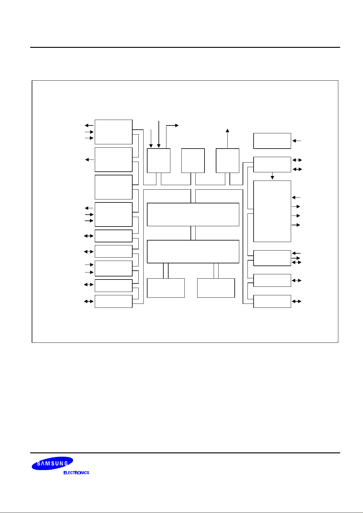
BLOCK DIAGRAM
X
XT
IN
TAOUT/TAPWM/P3.1
TACLK/P3.2
TACAP/P3.3
TBPWM/P3.0
T1CAP/P1.0
T1CLK/P1.1
T1OUT/T1PWM/P1.2
P0.0-P0.7/
INT0-INT7
8-Bit
Timer/
Counter A
8-Bit
Timer/
Counter B
16-Bit
Timer/
Counter 0
16-Bit
Timer/
Counter 1
I/O Port 0
RESET
IN
XOUT XTOUT
OSC/
RESET
I/O Port and Interrupt Control
Basic
Timer
BUZ/P1.4
Watch
Timer
Voltage
Detector
Voltage
Booster
LCD
Driver
VVLDREF
CB
CA
VLC0-VLC2
COM0-COM3
SEG0-SEG15
SEG16-SEG31
P1.0-P1.7
AVREF
AVSS
P2.0-P2.7/
ADC0-ADC7
P3.0-P3.4
I/O Port 1
A/D
Converter
I/O Port 2
I/O Port 3
SAM88 RC CPU
544/1056 Byte
Register File
16/32-Kbyte
ROM
Figure 1-1. Block Diagram
Serial I/O
Port
I/O Port 4
I/O Port 5
SI/P1.7
SO/P1.5
SCK/P1.6
P4.0-P4.7
P5.0-P5.7
1-3

PRODUCT OVERVIEW S3C8248/C8245/P8245/C8247/C8249/P8249
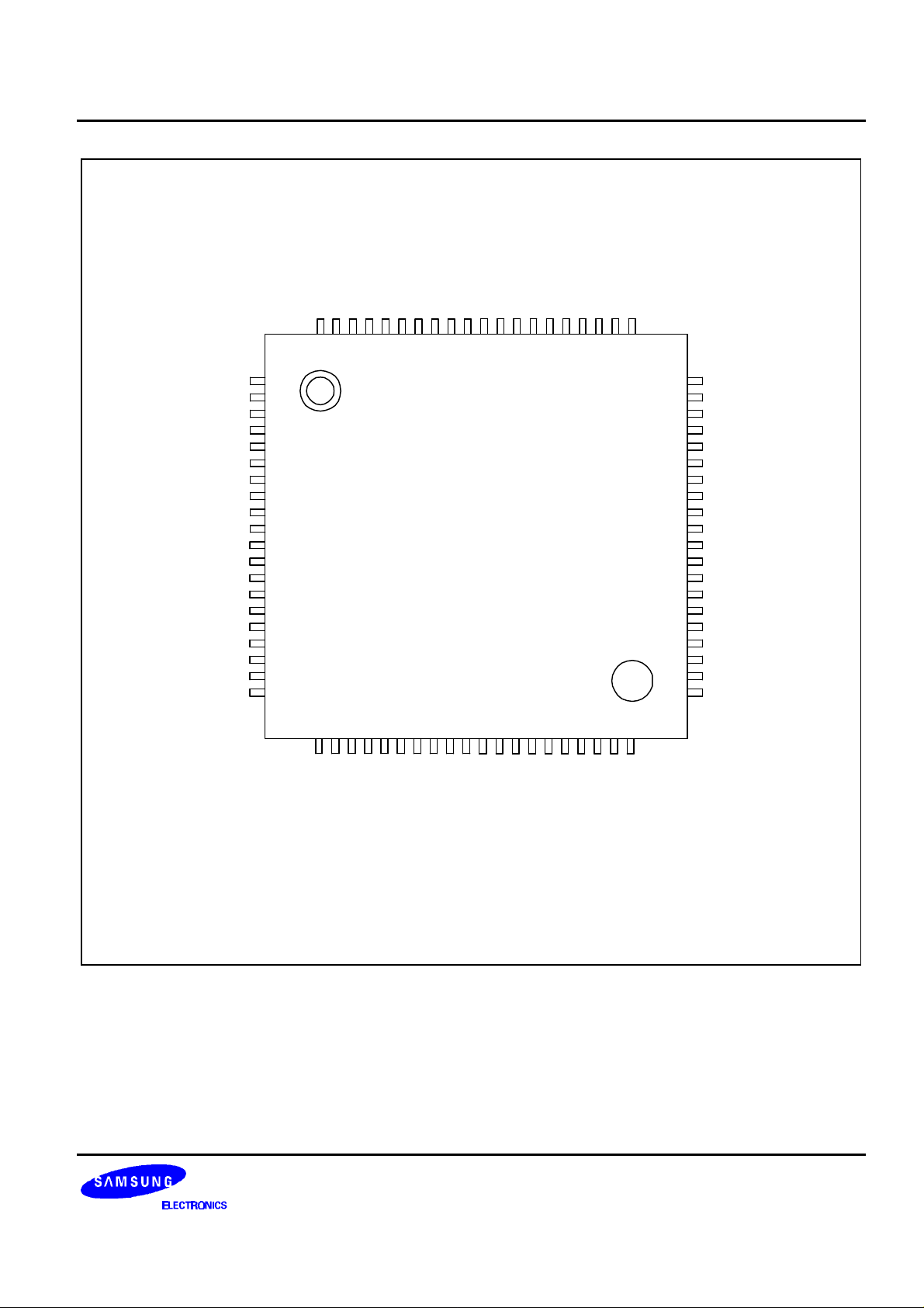
PIN ASSIGNMENT
SEG25/P5.1
SEG24/P5.0
SEG23/P4.7
SEG22/P4.6
SEG21/P4.5
SEG20/P4.4
SEG19/P4.3
SEG18/P4.2
SEG17/P4.1
SEG16/P4.0
SEG15
SEG14
SEG13
SEG12
SEG11
SEG10
SEG26/P5.2
SEG27/P5.3
SEG28/P5.4
SEG29/P5.5
SEG30/P5.6
SEG31/P5.7
P3.0/TBPWM
P3.1/TAOUT/TAPWM
P3.2/TACLK
P3.3/TACAP/SDAT
P3.4/SCLK
VDD
VSS
XOUT
XIN
TEST
XTIN
XTOUT
RESET
P0.0/INT0
P0.1/INT1
P0.2/INT2
P0.3/INT3
P0.4/INT4
1
2
3
4
5
6
7
8
9
10
11
12
13
14
15
16
17
18
19
20
21
22
23
24
807978777675747372717069686766
S3C8248/C8245
/C8247/C8249
(80-QFP-1420C)
65
64
SEG9
63
SEG8
62
SEG7
61
SEG6
60
SEG5
59
SEG4
58
SEG3
57
SEG2
56
SEG1
55
SEG0
54
COM3
53
COM2
52
COM1
51
COM0
50
VLC2
49
VLC1
48
VLC0
47
CA
46
CB
45
AVSS
44
AVREF
43
P2.7/ADC7/VVLDREF
42
P2.6/ADC6
41
P2.5/ADC5
1-4
252627282830313233343536373839
P1.3
P1.7/SI
P1.5/SO
P1.4/BUZ
P0.5/INT5
P0.6/INT6
P0.7/INT7
P1.0/T1CAP
P1.1/T1CLK
P1.2/T1OUT/T1PWM
P1.6/SCK
P2.0/ADC0
P2.1/ADC1
40
P2.2/ADC3
P2.3/ADC4
P2.4/ADC4
Figure 1-2. S3C8248/C8245/C8247/C8249 Pin Assignments (80-QFP)
S3C8248/C8245/P8245/C8247/C8249/P8249 PRODUCT OVERVIEW
SEG25/P5.1
SEG24/P5.0
SEG23/P4.7
SEG22/P4.6
SEG21/P4.5
SEG20/P4.4
SEG19/P4.3
SEG18/P4.2
SEG17/P4.1
SEG16/P4.0
SEG15
SEG14
SEG13
SEG12
SEG11
SEG10
SEG9
SEG8
SEG7
SEG6
SEG26/P5.2
SEG27/P5.3
SEG28/P5.4
SEG29/P5.5
SEG30/P5.6
SEG31/P5.7
P3.0/TBPWM
P3.1/TAOUT/TAPWM
P3.2/TACLK
P3.3/TACAP/SDAT
P3.4/SCLK
V
DD
V
X
OUT
X
TEST
XT
XT
OUT
RESET
P0.0/INT0
SS
80797877767574737271706968676665646362
1
2
3
4
5
6
7
8
9
10
11
12
13
S3C8248/C8245
/C8247/C8249
(80-TQFP-1212)
14
15
IN
16
17
IN
18
19
20
21222324252627282830313233343536373839
61
40
60
59
58
57
56
55
54
53
52
51
50
49
48
47
46
45
44
43
42
41
SEG5
SEG4
SEG3
SEG2
SEG1
SEG0
COM3
COM2
COM1
COM0
V
LC2
V
LC1
V
LC0
CA
CB
AV
SS
AV
REF
P2.7/ADC7/V
P2.6/ADC6
P2.5/ADC5
VLDREF
P1.3
P1.7/SI
P1.5/SO
P1.4/BUZ
P0.1/INT1
P0.2/INT2
P0.3/INT3
P0.4/INT4
P0.5/INT5
P0.6/INT6
P0.7/INT7
P1.0/T1CAP
P1.1/T1CLK
P1.6/SCK
P2.0/ADC0
P2.1/ADC1
P2.2/ADC3
P2.3/ADC4
P2.4/ADC4
P1.2/T1OUT/T1PWM
Figure 1-3. S3C8248/C8245/C8247/C8249 Pin Assignments (80-TQFP)
1-5

PRODUCT OVERVIEW S3C8248/C8245/P8245/C8247/C8249/P8249
PIN DESCRIPTIONS
Table 1-1. S3C8248/C8245/C8247/C8249 Pin Descriptions
Pin
Names
P0.0–P0.7 I/O I/O port with bit programmable pins;
Pin
Type
Pin
Description
Circuit
Type
Pin
Numbers
(note)
Share
Pins
D–4 20–27 INT0–INT7
Schmitt trigger input or output mode
selected by software; software assignable
pull-up. P0.0–P0.7 can be used as inputs
for external interrupts INT0–INT7
(with noise filter and interrupt control).
P1.0–1.7 I/O I/O port with bit programmable pins; Input
or output mode selected by software;
Open-drain output mode can be selected
by software; software assignable pull-up.
Alternately P1.0–P1.7 can be used as SI,
E–2 28-35 SI, SO, SCK,
BUZ, T1CAP
T1CLK
T1OUT
T1PWM
SO, SCK, BUZ, T1CAP, T1CLK, T1OUT,
T1PWM
P2.0–P2.7 I/O I/O port with bit programmable pins;
normal input and AD input or output
mode selected by software; software
assignable pull-up.
P3.0–P3.4 I/O I/O port with bit programmable pins. Input
or push-pull output with software
assignable pull-up. Alternately P3.0–P3.3
can be used as TACAP, TACLK, TAOUT,
TAPWM, TBPWM
F–10
F–18
36–42,
43
ADC0–ADC6
V
VLDREF
(ADC7)
D–2 7–11 TACAP
TACLK
TAOUT
TAPWM
TBPWM
P4.0–P4.7 I/O I/O port with bit programmable pins.
H–14 71–78 SEG16–SEG23
Push-pull or open drain output and input
with software assignable pull-up.
P4.0–P4.7 can alternately be used as
outputs for LCD SEG
P5.0–P5.7 I/O Have the same characteristic as port 4 H–14 79–6 SEG24–SEG31
1-6

S3C8248/C8245/P8245/C8247/C8249/P8249 PRODUCT OVERVIEW
Table 1-1. S3C8248/C8245/C8247/C8249 Pin Descriptions (Continued)
Pin
Names
ADC0–ADC6
ADC7
AV
REF
AV
SS
Pin
Type
I A/D converter analog input channels F–10
Pin
Description
Circuit
Type
F–18
Pin
Numbers
36–42
43
(note)
– A/D converter reference voltage – 44 –
– A/D converter ground – 45 –
Share
Pins
P2.0–P2.6
P2.7
INT0–INT7 I External interrupt input pins D–4 20–27 P0.0–P0.7
RESET
I System reset pin
B 19 –
(pull-up resistor: 250 kΩ)
TEST I 0 V: Normal MCU operating
– 16 –
5 V: Test mode
12 V: for OTP writing
SDAT, SCLK O Serial OTP interface pins; serial data
D–2 10, 11 P3.3, P3.4
and clock
V
DD, VSS
– Power input pins for CPU operation
– 12, 13 –
(internal) and Power input for OTP
Writing
X
OUT, XIN
– Main oscillator pins – 14, 15 –
SCK, SO, SI I/O Serial I/O interface clock signal E–2 33–35 P1.5–P1.7
V
VLDREF
I Voltage detector reference voltage
F–18 43 P2.7
input
TACAP I Timer A Capture input D–2 10 P3.3
TACLK I Timer A External clock input D–2 9 P3.2
TAOUT/TAPWM O Timer A output and PWM output D–2 8 P3.1
TBPWM O Timer B PWM output D–2 7 P3.0
T1CAP I Timer 1 Capture input E–2 28 P1.0
T1CLK I Timer 1 External clock input E–2 29 P1.1
T1OUT/T1PWM O Timer 1 output and PWM output E–2 30 P1.2
COM0–COM3 O LCD common signal output H 51–54 –
SEG0–SEG15 O LCD segment output H 55–70 –
SEG16–SEG23 O LCD segment output H–14 71–78 P4.0–P4.7
SEG24–SEG31 O LCD Segment output H–14 79–6 P5.0–P5.7
V
LC0–VLC2
BUZ O 0.5, 1, 2 or 4 kHz frequency output for
O LCD power supply – 48–50 –
E–2 32 P1.4
buzzer sound with 4.19 MHz main
system clock or 32768 Hz subsystem
clock
CA, CB – Capacitor terminal for voltage booster – 46–47 –
1-7

PRODUCT OVERVIEW S3C8248/C8245/P8245/C8247/C8249/P8249
Disable
PIN CIRCUITS
VDD
VDD
Pull-up
Enable
P-Channel
In
Figure 1-4. Pin Circuit Type B (RESETRESET)
V
DD
Data
Output
P-Channel
N-Channel
Out
Data
Output
Disable
Circuit
Type C
Figure 1-6. Pin Circuit Type D-2 (P3)
VDD
VDD
Data
Output
Disable
Pin Circuit
Type C
I/O
Pull-up
Enable
I/O
1-8
Figure 1-5. Pin Circuit Type C
Noise
Ext.INT
Input
Normal
Filter
Figure 1-7. Pin Circuit Type D-4 (P0)

S3C8248/C8245/P8245/C8247/C8249/P8249 PRODUCT OVERVIEW
VDD
VDD
Open drain
Enable
VDD
Pull-up
Resistor
Pull-up
Enable
Data
Output
Disable
Schmitt Trigger
Figure 1-8. Pin Circuit Type E-2 (P1)
Pull-up
Enable
P-CH
N-CH
VDD
I/O
Data
Output
Disable
ADC & VLD
Enable
Data
VLDREF
To ADC
Circuit
Type C
Figure 1-10. Pin Circuit Type F-18 (P2.7/VLD
VLC2
VLC1
I/O
REF
)
Data
Output
Disable
ADCEN
Data
To ADC
Circuit
Type C
Figure 1-9. Pin Circuit Type F-10 (P2.0–P2.6)
I/O
SEG/
COM
VLC0
Figure 1-11. Pin Circuit Type H (SEG/COM)
Out
1-9

PRODUCT OVERVIEW S3C8248/C8245/P8245/C8247/C8249/P8249
VLC2
VLC1
SEG
Output
Disable
VLC0
Open Drain EN
Data
LCD Out EN
SEG
Output
Disable
Figure 1-12. Pin Circuit Type H-4
VDD
VDD
Pull-up
Enable
Circuit
Type H-4
1-10
Figure 1-13. Pin Circuit Type H-14 (P4, P5)
 Loading...