

Samsung KS88C01632, KS88C01624, KS88C01532, KS88C01524, S3C80G9 Datasheet
...
S3C80F7/C80F9/C80G7/C80G9 (KS88C01524/C01532/C01624/C01632) PRODUCT OVERVIEW
1 PRODUCT OVERVIEW
S3C8-SERIES MICROCONTROLLERS
Samsung's S3C8 series of 8-bit single-chip CMOS microcontrollers offers a fast and efficient CPU, a wide range
of integrated peripherals, and various mask-programmable ROM sizes. Important CPU features include:
— Efficient register-oriented architecture
— Selectable CPU clock sources
— Idle and Stop power-down mode release by interrupt
— Built-in basic timer with watchdog function
A sophisticated interrupt structure recognizes up to eight interrupt levels. Each level can have one or more
interrupt sources and vectors. Fast interrupt processing (within a minimum six CPU clocks) can be assigned to
specific interrupt levels.
S3C80F7/C80F9/C80G7/C80G9 Microcontroller
The S3C80F7/C80F9/C80G7/C80G9 single-chip CMOS microcontroller is fabricated using a highly advanced
CMOS process and is based on Samsung's newest CPU architecture.
The S3C80F9/C80G9 is the microcontroller which has 32-Kbyte mask-programmable ROM and S3C80F7/C80G7
is the microcontroller which has 24-Kbyte mask-programmable ROM.
The S3P80F9/P80G9 is the microcontroller which has 32-Kbyte one-time-programmable EPROM and
S3P80F7/P80G7 is the microcontroller which has 24-Kbyte one-time-programmable EPROM.
Using a proven modular design approach, Samsung engineers developed S3C80F7/C80F9/C80G7/C80G9 by
integrating the following peripheral modules with the powerful SAM87 RC core:
— Internal LVD circuit and 16 bit-programmable pins for external interrupts.
— One 8-bit basic timer for oscillation stabilization and watchdog function (system reset).
— One 8-bit timer/counter and one 16-bit timer/counter with selectable operating modes.
— One 8-bit counter with auto-reload function and one-shot or repeat control.
The S3C80F7/C80F9/C80G7/C80G9 is a versatile general-purpose microcontroller which is especially suitable
for use as remote transmitter controller. It is currently available in a 32-pin SOP, 42-pin SDIP and 44-pin QFP
package.
1-1

PRODUCT OVERVIEW S3C80F7/C80F9/C80G7/C80G9 (KS88C01524/C01532/C01624/C01632)
FEATURES
CPU
• SAM87RC CPU core
Memory
• 32-Kbyte internal ROM (S3C80F9/C80G9)
: 0000H–7FFFH
• 24-Kbyte internal ROM (S3C80F7/C80G7)
: 0000H–5FFFH
• Data memory: 272-byte RAM (318 register)
Instruction Set
• 78 instructions
• IDLE and STOP instructions added for power-
down modes
Instruction Execution Time
• 500 ns at 8-MHz f
(minimum)
OSC
Interrupts
• 22 interrupt sources with 16 vector and 7 level.
I/O Ports
• Three 8-bit I/O ports (P0–P2), one 8-bit output
port(P4) and 6-bit port (P3) for a total of 38 bitprogrammable pins.(44-QFP)
• Three 8-bit I/O ports (P0–P2), one 8-bit output
port(P4) and 4-bit port (P3) for a total of 36 bitprogrammable pins.(42-SDIP)
• Three 8-bit I/O ports (P0–P2) and one 2-bit I/O
port (P3) for a total of 26-bit programmable pins.
(32-SOP)
Carrier Frequency Generator
• One 8-bit counter with auto-reload function and
one-shot or repeat control (Counter A)
Back-up mode
• When V
is lower than V
DD
, the chip enters
LVD
Back-up mode to block oscillation and reduce
the current consumption.
In S3C80G7/C80G9, this function is disabled
when operating state is “STOP mode”.
• When RESET pin is lower than Input Low
Voltage (VIL), the chip enters Back-up mode to
block oscillation and reduce the current
consumption.
Low Voltage Detect Circuit
• Low voltage detect to get into Back-up mode.
• Low level detect voltage
− S3C80F7/C80F9: 2.20 V (Typ) ± 200mV
− S3C80G7/C80G9: 1.90 V (Typ) ± 200mV
Operating Temperature Range
• –40
°
C to + 85 °C
Operating Voltage Range
• 1.7V to 5.0V at 4 MHz f
• 2.0V to 5.0V at 8 MHz f
(S3C80G7/C80G9)
OSC
(S3C80F7/C80F9)
OSC
Package Type
• 44-pin QFP-1010B
• 42-pin SDIP
Timers and Timer/Counters
• One programmable 8-bit basic timer (BT) for
oscillation stabilization control or watchdog timer
(software reset) function
• One 8-bit timer/counter (Timer 0) with three
operating modes; Interval mode, Capture and
PWM mode.
• One 16-bit timer/counter (Timer1) with two
operating modes; Interval mode and Capture.
1-2
• 32-pin SOP

S3C80F7/C80F9/C80G7/C80G9 (KS88C01524/C01532/C01624/C01632) PRODUCT OVERVIEW
BLOCK DIAGRAM
XIN
XOUT
VDD
MAIN
OSC
8-Bit
Basic
Timer
8-Bit
Timer/
Counter
16-Bit
Timer/
Counter
P0.0-0.3 (INT0-INT3)
P0.4-P0.7 (INT4)
LVD
I/O Port and Interrupt
32K-Bytes
ROM
Port 0
Control
SAM87RC
CPU
P1.0-P1.7
Port 1
317-Bytes
Register
File
TEST
RESET
Port 2
Port 3
Port 4
P2.0-2.3 (INT5-INT8)
P2.4-2.7 (INT9)
P3.0-T0PWM/
T0CAP/(T1CAP)
P3.1-REM/(T0CK)
P3.2/(T0CK)
P3.3/(T1CAP)
P3.4-3.5
P4.0-4.7
Figure 1-1. Block Diagram
Carrier
Registor
(Counter A)
1-3
PRODUCT OVERVIEW S3C80F7/C80F9/C80G7/C80G9 (KS88C01524/C01532/C01624/C01632)
PIN ASSIGNMENTS
P4.2
P4.1
P4.0
P2.0/INT5
P2.1/INT6
P2.2/INT7
P2.3/INT8
P2.4/INT9
P3.0/T0PWM/T0CAP/SDAT
R3.1/REM/SCLK
VDD
VSS
XOUT
XIN
TEST
P2.5/INT9
P2.6/INT9
RESET
P2.7/INT9
P1.0
P3.2/T0CK
1
2
3
4
5
6
7
8
9
10
11
12
13
14
15
16
17
18
19
20
21
S3C80F7/C80F9
/C80G7/C80G9
(Top View)
42-SDIP
42
41
40
39
38
37
36
35
34
33
32
31
30
29
28
27
26
25
24
23
22
P4.3
P0.7/INT4
P0.6/INT4
P0.5/INT4
P0.4/INT4
P0.3/INT3
P0.2/INT2
P0.1/INT1
P0.0/INT0
P4.4
P4.5
P4.6
P1.7
P1.6
P1.5
P1.4
P1.3
P1.2
P1.1
P4.7
P3.3/T1CAP
1-4
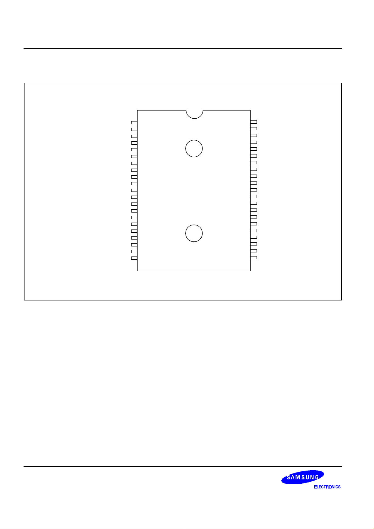
Figure 1-2. Pin Assignment Diagram (42-Pin SDIP Package)
S3C80F7/C80F9/C80G7/C80G9 (KS88C01524/C01532/C01624/C01632) PRODUCT OVERVIEW
P3.0/T0PWM/T0CAP/
P0.3/INT3
P0.2/INT2
P0.1/INT1
P0.0/INT0
P4.4
P4.5
P4.6
P1.7
P1.6
P1.5
P1.4
3332313029282726252423
P0.4/INT4
P0.5/INT4
P0.6/INT4
P0.7/INT4
P4.3
P4.2
P4.1
P4.0
P2.0/INT5
P2.1/INT6
P2.2/INT7
34
35
S3C80F7/C80F9
36
37
38
39
40
41
42
43
44
/C80G7/C80G9
(Top View)
(44-QFP)
1234567891011
22
21
20
19
18
17
16
15
14
13
12
P1.3
P1.2
P1.1
P4.7
P3.3/T1CAP
P3.2/T0CK
P1.0
P2.7/INT9
P3.5
P3.4
RESET
XIN
VSS
VDD
XOUT
SDAT
P2.3/INT8
P2.4/INT9
P3.1/REM/SCLK
TEST
P2.5/INT9
P2.6/INT9
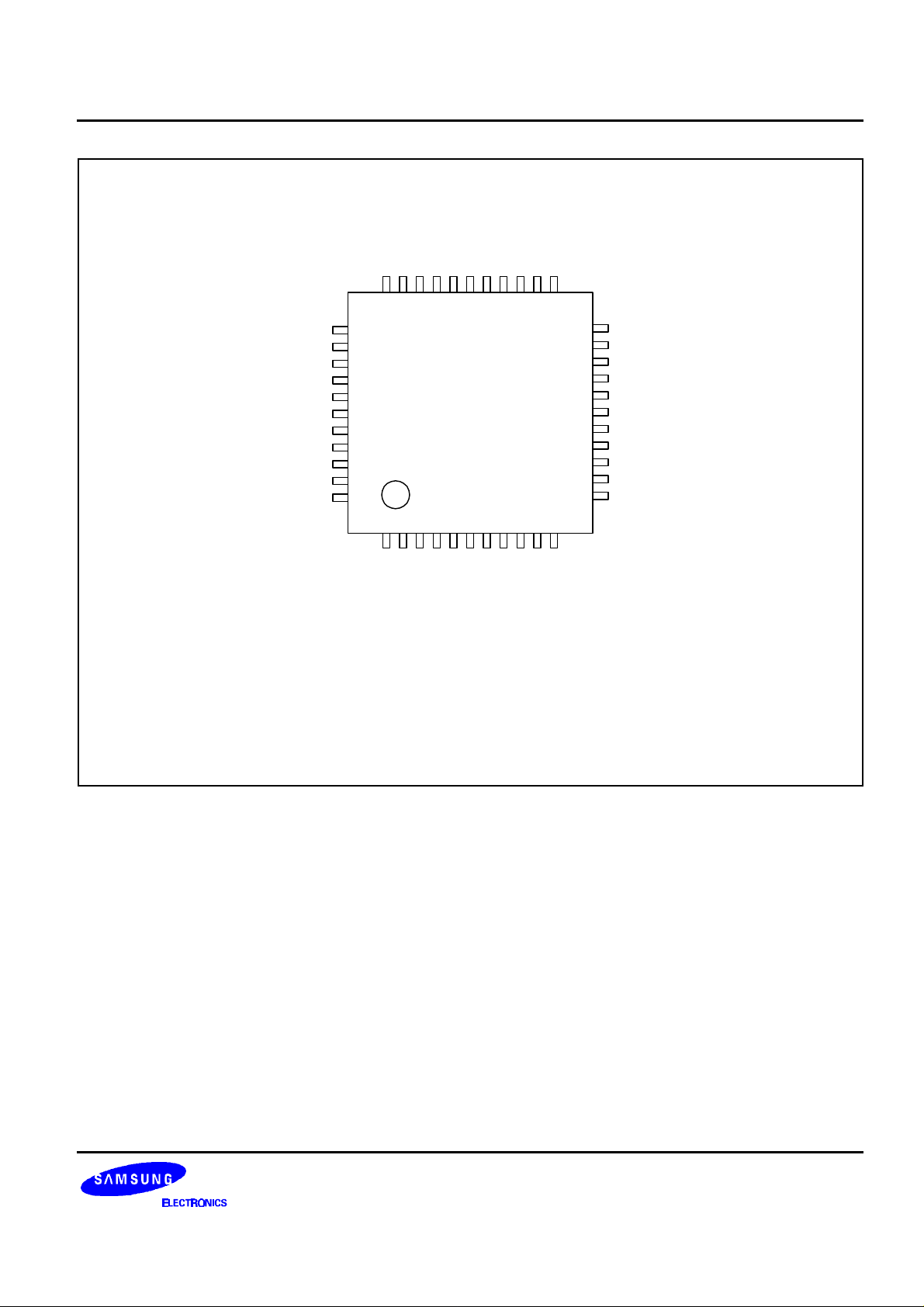
Figure 1-3. Pin Assignment Diagram (44-Pin QFP Package)
1-5

PRODUCT OVERVIEW S3C80F7/C80F9/C80G7/C80G9 (KS88C01524/C01532/C01624/C01632)
VSS
XIN
XOUT
TEST
P2.5/INT9
P2.6/INT9
RESET
P2.7/INT9
P1.0
P1.1
P1.2
P1.3
P1.4
P1.5
P1.6
P1.7
1
2
3
4
5
S3C80F7/C80F9
6
7
/C80G7/C80G9
8
9
10
11
12
13
14
15
16
(Top View)
32-SOP
32
31
30
29
28
27
26
25
24
23
22
21
20
19
18
17
VDD
P3.1/REM/T0CK/SCLK
P3.0/T0PWM/T0CAP/T1CAP/SDAT
P2.4/INT9
P2.3/INT8
P2.2/INT7
P2.1/INT6
P2.0/INT5
P0.7/INT4
P0.6/INT4
P0.5/INT4
P0.4/INT4
P0.3/INT3
P0.2/INT2
P0.1/INT1
P0.0/INT0
Figure 1-4. Pin Assignment Diagram (32-Pin SOP Package)
1-6
S3C80F7/C80F9/C80G7/C80G9 (KS88C01524/C01532/C01624/C01632) PRODUCT OVERVIEW
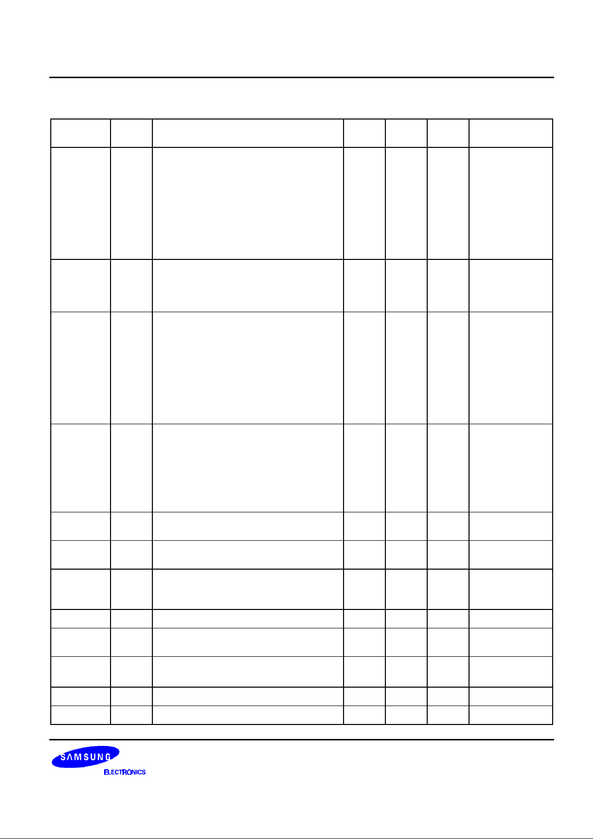
Table 1-1. Pin Descriptions of 44-QFP and 42-SDIP
Pin
Names
P0.0–P0.7 I/O I/O port with bit-programmable pins.
Pin
Type
Pin Description Circuit
Type
1 34–41 30–37 Ext. INT
42 Pin
No.
Configurable to input or push-pull output
mode. Pull-up resistors can be assigned
by software. Pins can be assigned
individually as external interrupt inputs
with noise filters, interrupt enable/
disable, and interrupt pending control.
SED & R circuit built in P0 for STOP
releasing.
P1.0–P1.7 I/O I/O port with bit-programmable pins.
Configurable to input mode or output
2 20
24–301620–26
mode. Pin circuits are either push-pull or
n-channel open-drain type.
P2.0–P2.3
P2.4–P2.7
I/O I/O port with bit-programmable pins.
Configurable to input or push-pull output
mode. Pull-up resistors can be assigned
1 4–8,
16, 17
19
by software. Pins can be assigned
individually as external interrupt inputs
with noise filters, interrupt enable/
disable, and interrupt pending control.
SED & R circuit built in P2 for STOP
releasing.
P3.0
P3.1
I/O 2-bit I/O port with bit-programmable pins.
Configurable to input mode, push-pull
3
9–10 3–4 T0PWM/ T0CAP
4
output mode, or n-channel open-drain
output mode. Input mode with pull-up
resistors can be assigned by software.
The two port 3 pins have high current
drive capability
P3.2–P3.3 I C-MOS Input port with pull-up resistors 5 21
22
P3.4–P3.5 O Open drain output port for high current
6 None 13–14 –
drive
P4.0–P4.7 O 8- bit-programmable output pins.
Configurable to open drain output port or
push-pull output port.
XIN, X
RESET
OUT
– System clock input and output pins – 13,14 7,8 –
I System reset signal input pin and back-
7 1–3
42,23
31-33
8 18 12 –
up mode input.
TEST I Test signal input pin (for factory use only;
– 15 9 –
must be connected to VSS.)
44 Pin
No.
42–44
1,2,
10,11,
15
17
18
41–38
27–29
19
Shared
Functions
(INT0 - 4)
–
Ext. INT
(INT5–9)
REM
(T0CK)
(T1CAP)
–
V
DD
V
SS
– Power supply input pin – 11 5 –
– Ground pin – 12 6 –
1-7
PRODUCT OVERVIEW S3C80F7/C80F9/C80G7/C80G9 (KS88C01524/C01532/C01624/C01632)
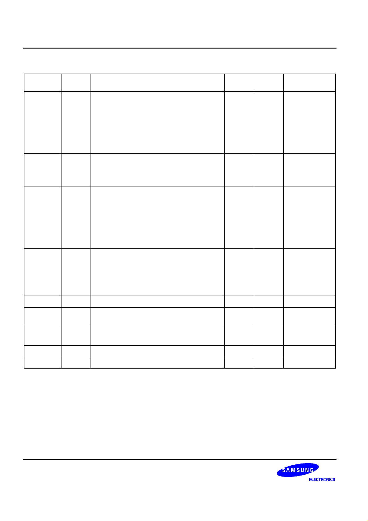
Table 1-2. Pin Descriptions of 32-SOP
Pin
Names
Pin
Type
Pin Description Circuit
P0.0–P0.7 I/O I/O port with bit-programmable pins.
Configurable to input or push-pull output
mode. Pull-up resistors are assignable by
software. Pins can be assigned individually as
external interrupt inputs with noise filters,
interrupt enable/ disable, and interrupt pending
control. SED & R circuit built in P0 for STOP
releasing.
P1.0–P1.7 I/O I/O port with bit-programmable pins.
Configurable to input mode or output mode.
Pin circuits are either push-pull or n-channel
open-drain type.
P2.0–P2.3
P2.4–P2.7
I/O I/O port with bit-programmable pins.
Configurable to input or push-pull output
mode. Pull-up resistors can be assigned by
software. Pins can be assigned individually as
external interrupt inputs with noise filters,
interrupt enable/disable, and interrupt pending
control. SED & R circuit built in P2 for STOP
releasing.
P3.0
P3.1
I/O 2-bit I/O port with bit-programmable pins.
Configurable to input mode, push-pull output
mode, or n-channel open-drain output mode.
Input mode with pull-up resistors can be
assigned by software. The two port 3 pins
have high current drive capability.
XIN, X
RESET
OUT
– System clock input and output pins – 2,3 –
I System reset signal input pin and back-up
mode input.
TEST I Test signal input pin (for factory use only;
must be connected to VSS).
Type
32 Pin
No.
Shared
Functions
1 17–24 Ext. INT
2 9–16 –
1 25–28
Ext. INT
29,5, 6,8
3
4
30,31 T0PWM/
T0CAP/T1CAP
REM/T0CK
8 7 –
– 4 –
V
V
1-8
DD
SS
– Power supply input pin – 32 –
– Ground pin – 1 –
S3C80F7/C80F9/C80G7/C80G9 (KS88C01524/C01532/C01624/C01632) PRODUCT OVERVIEW
PIN CIRCUITS
VDD
Pull-up
Resistor
Pull-up
Enable
VDD
Data
Input/
Output
Output
Disable
VSS
External
Interrupt
Stop
Noise
Filter
Stop release
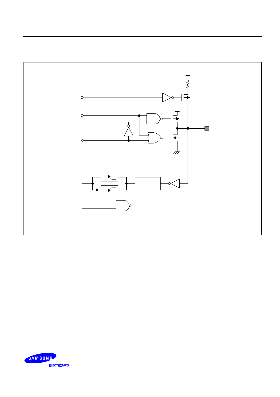
Figure 1-5. Pin Circuit Type 1 (Port 0 and Port2)
1-9
PRODUCT OVERVIEW S3C80F7/C80F9/C80G7/C80G9 (KS88C01524/C01532/C01624/C01632)
PIN CIRCUITS (Continued)
VDD
Pull-up
Resistor
Pull-up
Enable
VDD
Data
Input/
Output
Open-Drain
Output Disable
VSS
Normal
Input
Noise
Filter
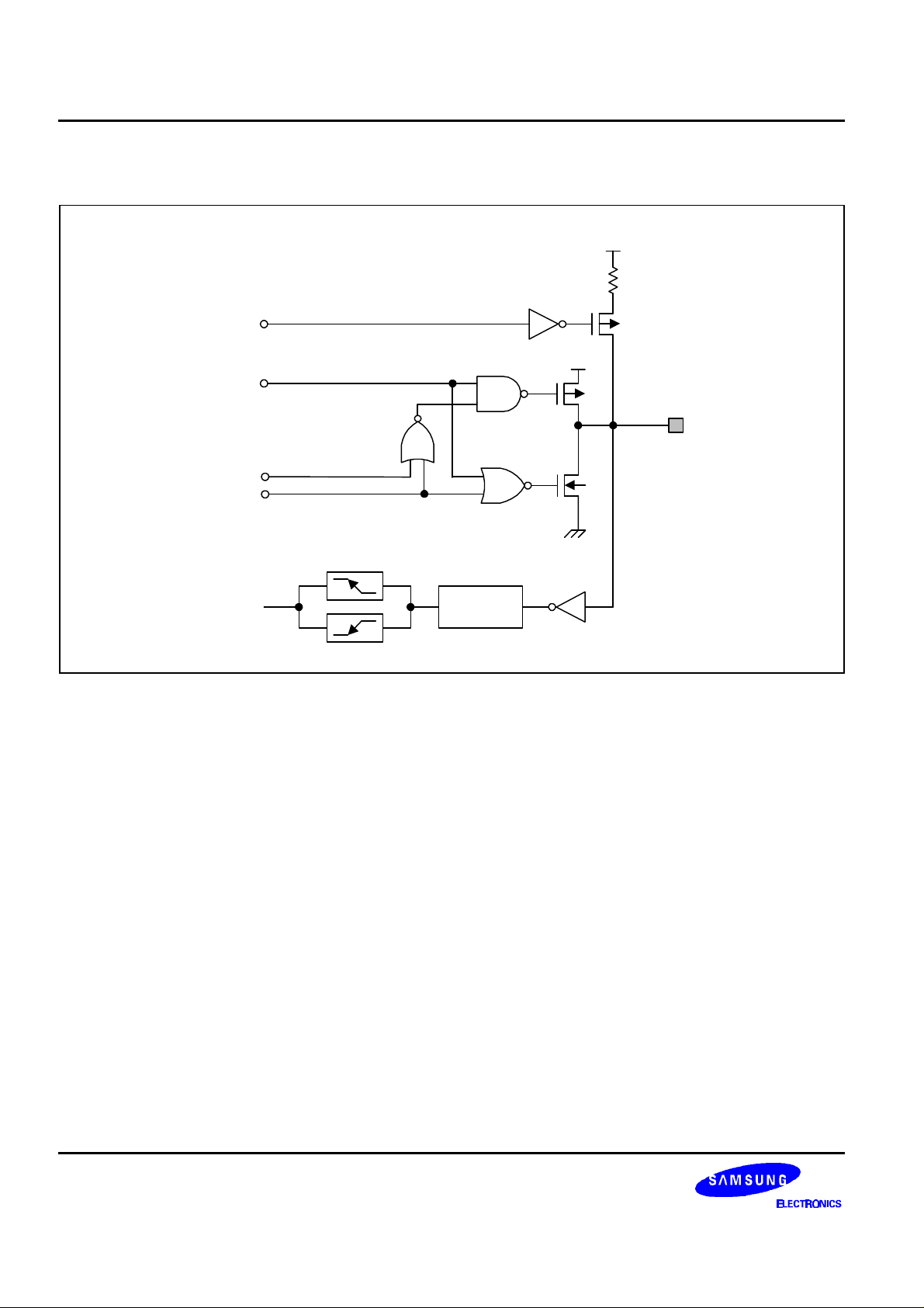
Figure 1-6. Pin Circuit Type 2 (Port 1)
1-10
S3C80F7/C80F9/C80G7/C80G9 (KS88C01524/C01532/C01624/C01632) PRODUCT OVERVIEW
PIN CIRCUITS (Continued)
VDD
Pull-up
Resistor
Pull-up
Enable
P3CON.2
VDD
Port 3.0 Data
T0_PWM
Open-Drain
Output Disable
P3.0 Input
T0CAP/(T1CAP)
M
U
X
P3CON.2,6,7
M
U
X
Data
VSS
Noise filter
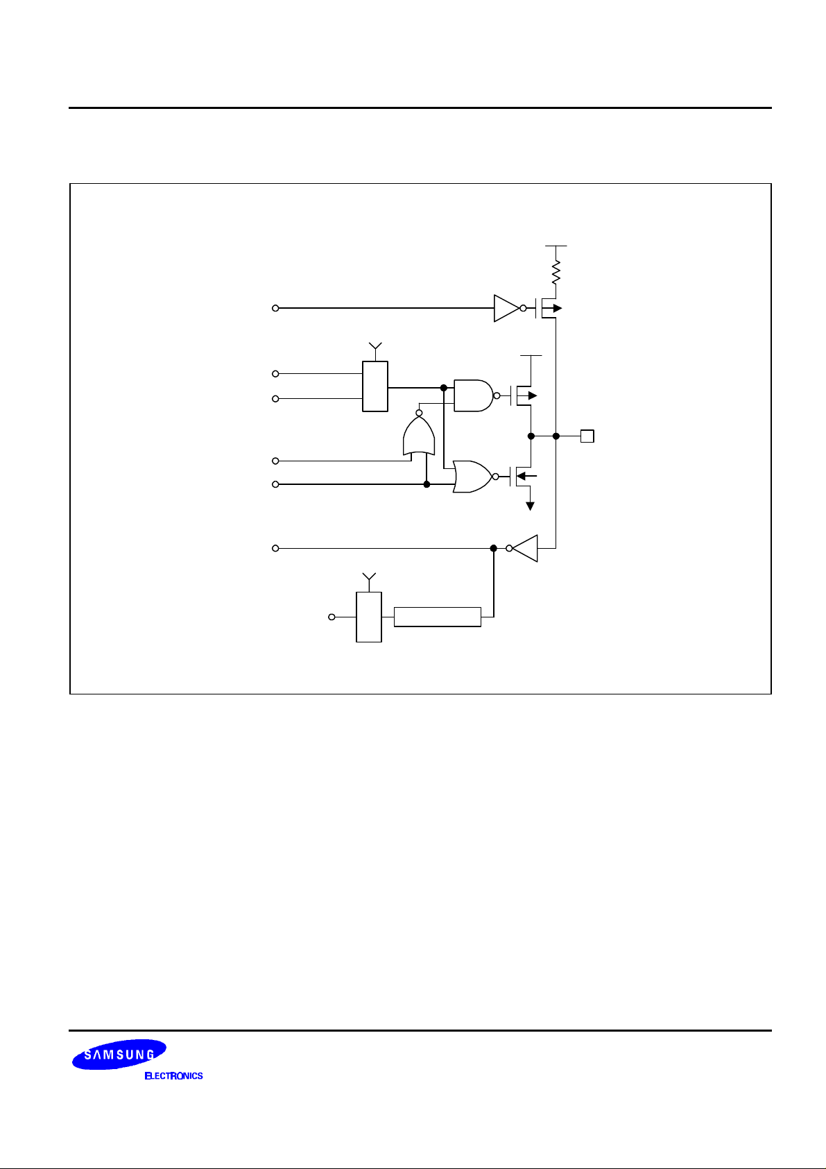
Figure 1-7. Pin Circuit Type 3 (P3.0)
P3.0/T0PWM
T0CAP/(T1CAP)
1-11
 Loading...