

Page 1

Circuit Operation Description
Samsung Electronics 5-1
5. Circuit Description
5-1 Power supply
5-1-1 Outline(PDP SMPS)
Considering various related conditions, the switching regulator with good efficiency and allowing for its
small size and lightweight was used as the power supply for PDP. Most of the power supply components
used forward converter, and Vsamp and Vsb used simple flyback converter.
To comply with the international harmonics standards and improve the power factor, active PFC (Power
Factor Correction) was used to rectify AC input into +400V DC output, which in turns used as input to the
switching regulator.
5-1-2 42"SD SMPS SPECIFICATION
5-1-2(A) INPUT
PDP-42PS board is designed so that input power can be used within AC 90 VAC to 264 VAC with
50/60Hz ± 3Hz.
5-1-2(B) OUTPUT
PDP-42PS board provides 13 output switching power supplies for PDP 50inch (+165Vs, +220Set, +185Ve,
+75Va, +80Scan, +18Vg, +5Vsb, +5V(D), +5V(A), +12V. +9V, +12Vfan, and +12Vsamp). The output voltage, and current requirements for continuous operation are stated below (Table 3).
Table1. Specifications of Output Power Supplies for PDP SMPS
Output Name
Vs
Va
Vscan
Vset
Ve
Vg
Vfan
V9
V5(A)
V5(D)
Vsb
V12
Vsamp
Output Voltage
+165V
+75V
+80V
+220V
+185V
+18.3V
+12V
+9V
+5V
+5.3V
+5V
+12V
+12V
Output Current
1.4A
0.5A
0.05A
0.05A
0.05A
0.3A
0.8A
0.3A
1.0A
3.5A
0.4
1.2A
1.5A
Using in PDP driving
Sustain Voltage of Drive Board
Address Voltage of Drive Board
Analog IC Drive Voltage of Video Board
IC Drive Voltage of Logic Board
Stand-by for Remote Control
Page 2

Circuit Operation Description
5-2 Samsung Electronics
Table 2. Specifications to Protect PDP SMPS
Division
Vs
Va
+5V
OCP Current
5A
2A
10A
OVP Voltage
195V
90V
6.2V
Short Circuit
O.K
O.K
O.K
5-1-2(C) FUNCTION OF BOARD
(1) Remote control
Using 250V/ 10A relay, the board makes remote control available.
(2) Free voltage
The board designed so that input voltage can be used within 90 VAC to 264VAC.
(3) Embedded thermal sensor
The board is equipped with thermal sensor to detect the internal temperature of the unit, and to short
relay when the internal temperature is higher than specified temperature so as to shutdown the unit.
(4) Improvement of power factor
The board is designed using PFC circuit so that PF (Power Factor) can be over 0.95, because low PF
can be a problem in high voltage power.
(5) Protection
The OCP (Over Current Protection), the OVP (Over voltage Protection), and the Short Circuit
Protection functions are added against system malfunction.
Page 3

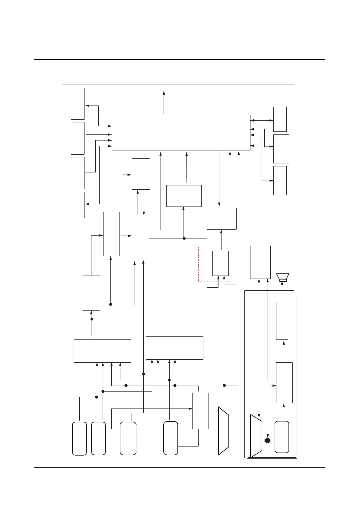
Circuit Operation Description
Samsung Electronics 5-3
5-1-2(D) PDP-PS-42 BLOCK DIAGRAM
Page 4

Circuit Operation Description
5-4 Samsung Electronics
(1) AC-DC Converter
PDP-42PS outputs +400V DC from the common AC power supply using the active PFC booster converter. This converter is designed for improving the power factor and preventing the noise with high
frequency and finally becomes the input power system for the switching regulator on the output side.
(2) Auxiliary Power Supply
The auxiliary power supply is a block generating power of •Ï-com for remote controlling. Once the
power plug is inserted, this block always comes into operation, causing •Ï-com to get into the standby state for the output. Thus, this output is called the stand-by voltage. And with the relay ON signal
inputted through the remote controller, this block turns the mechanical switch of relay to ON for driving the main power supply.
(3) Implementation of Sustain Voltage
As the main part of a SMPS for PDP, sustain voltage must supply a high power, +165V/ 1.4A. It is
designed using forward converter basically. At the output stage two 90V converters are connected
serially for high efficiency and reduction of system size against a single 180V converter.
(4) Implementation of Small Power Output (Va, V(D), V(A), Vfan, V9, Vsamp, Ve, Vset, Vscan, V12, and
Vg)Vset, Ve, and Vscan used DC-DC module. V(D), Va, V12, and Vfan used forward converter, and
Vsamp used flyback converter. V(A), V9, and Vg are simply implemented using switching regulator.
5-1-3 Requirements of PDP SMPS
Since SMPS does not operate alone, but it operates with the load of the whole system, it should be designed
carefully considering the load of the system. In addition, it should be designed considering emerging issues
such as EMC, and protection against heat as well as system stability especially.
5-1-3(A) SAFETY AND REMOTE CONTROL CAPABILITY
Stability is one of the most important requirements for SMPS. SMPS should be designed to prevent
abnormal status due to abnormal load variation so as to keep the system stable, and guarantee customer
safety.
The protection circuits of SMPS include over-current protection (OCP), over voltage protection (OVP),
and under voltage lock-out (UVLO), and short circuit protection circuit. Although each circuit can be
implemented by various procedures, the most popular is implementing with comparator that compares
current value with that of standard and determine abnormality of the circuit.
In addition, surge current protection, insulation management, and static electricity protection circuit
should be added, because it uses commercial power source as an input.
PDP SMPS should be designed using auxiliary power and relay to provide remote control capability.
Page 5

Circuit Operation Description
Samsung Electronics 5-5
5-1-3(B) THE RELATION BETWEEN POWER CONSUMPTION AND POWER CONVERSION Efficiency
The power consumption and the power conversion efficiency of SMPS affect protection against heat and
system operation much.
[ If the power conversion efficiency of 100W SMPS is 70%, is the power loss of internal circuit 30W? ]
Output power consumption Po is determined by the multiplication of DC output voltage Vo and output
current Io. Input power consumption Pi is determined by the addition of output power consumption
Po and internal power loss of SMPS Pl.
Provided that the power conversion efficiency is _,
If the power conversion efficiency of 100W SMPS is 70%, the internal power loss is about 42.8W by
Equation (1). If the power conversion efficiency of 400W SMPS for 42"SD is 82%, the internal power loss
is 87.8W by Equation (1). Table 4 shows internal power loss as a function of output power for various
power conversion efficiencies.
Table 4. Power Conversion Efficiency vs. Internal Power Loss
0
20
40
60
80
100
120
140
160
180
200
120 140 160 180 200 240220 260 280 300
50%
60%
90%
70%
80%
η
=
η
=
η
=
η
=
η
=
Internal
Power
Loss ( W)
Direct Current Output Power (W)
Page 6

Circuit Operation Description
5-6 Samsung Electronics
5-1-3(C) PFC (Power Factor Correction) Circuit Descriptions
The current electric devices use DC power supply and require a rectifier circuit converting AC into DC.
As most rectifier circuits apply a capacitor input type, the rectifier circuit becomes the core of the occurrence of harmonics with lower reverse rate.If various electronic and electric devices are connected to a
power system, high-frequency current will occur due to a power rectifier circuit, a phase control circuit
with power input current of non-sine wave, or components with non-linear load characteristics, such as
capacitor, inductor, etc. As the result, the disturbance of voltage occurs, and finally a power capacitor or
a transformer generates heat, fire or noise occurs, controls malfunction, or the accessed devices abnormally operate or their lives are shortened.To prevent those symptoms, IEC (International
Electrotechnical Commission) regulated standards for Power Supply Harmonics.
(Refer to IEC 1000-3-2.)Figure 8 shows the basic structure of Active Boost PFC and waveforms.
Standards for Power Supply Harmonics
Scale: Devices accessed to 220V/380V, 230V/400V, 240V/425V and lower than 16A (IEC 100-3-2)
Devices with AC 230V and lower than 16A (IEC 555-2)
Applied Classes :
♣ Class A: Devices not included in another class
♣ Class B : Portable tools
♣ Class C : Lighting devices
♣ Class D : Devices with special current waveforms
Application Schedule : Except the devices less than rating input of 75W (1996~1999)
Except the devices less than rating input of 50W (2000 and after)
Page 7

Circuit Operation Description
Samsung Electronics 5-7
5-1-3(D) CONCLUSION
Although SMPS (Switching Mode Power Supply) enables small lightweight high-power consumption
power design, it is hard to be used when stability and precise control are required. Power stage for PDP
can be designed using the lightweight SMPS feature. It is important to design SMPS considering
system load, stability, and related international standards.
The architecture and the pulse of active boost PFC
Page 8

Circuit Operation Description
5-8 Samsung Electronics
5-2 Driver Circuit
5-2-1 Driver Circuit Overview
5-2-1(A) WHAT IS THE DEFINITION OF DRIVE CIRCUIT?
It is a circuit generating an appropriate pulse (High voltage pulse) and then driving the panel to implement
images in the external terminals (X electrode group, Y electrode group and address electrode), and this high
voltage switching pulse is generated by a combination of MOSFET’s.
5-2-1(B) PANEL DRIVING PRINCIPLES
In PDP, images are implemented by impressing voltage on the X electrode, Y electrode and address electrode, components of each pixel on the panel, under appropriate conditions. Currently, ADS (Address &
Display Separate: Driving is made by separating address and sustaining sections) is most widely used to
generate the drive pulse. Discharges conducted within PDP pixels using this method can largely be classified into 3 types, as follows:
(1) Address discharge : This functions to generate wall voltage within pixels to be lighted by addressing
information to them (i.e., impressing data voltage)
(2) Sustain discharge : This means a display section where only pixels with wall voltage by the address
discharge display self-sustaining discharge by the support of such wall voltage. (Optic outputs realizing images are generated.)
(3) Erase discharge : To have address discharge occur selectively in pixels, all pixels in the panel must
have the same conditions (i.e., the same state of wall and space electric discharges). The ramp reset
discharge section, therefore, is important to secure the drive margin, and methods most widely used
to date include wall voltage controlling by ramp pulse.
Page 9

Circuit Operation Description
Samsung Electronics 5-9
5-2-1(C) TYPES AND DETAILED EXPLANATION OF DRIVE DISCHARGES
(1 ) Sustaining discharge
Sustaining discharge means a self-sustaining discharge generated by the total of the sustaining pulse
voltage (usually, 160~170V) alternately given to X and Y electrodes during the sustaining period and
the wall voltage that varies depending upon pixels' previous discharge status. It is operated by the
memory function (through this, the current status is defined by previous operation conditions) AC
PDP basically possesses. That is, when there is existing wall voltage in pixels (in other words, when
pixels remain ON), the total of wall voltage and a sustaining voltage to be impressed subsequently
impresses a voltage equal to or above the discharge start voltage, thereby generating discharge again,
but when there is no existing wall voltage in pixels (in other words, when pixels remain OFF), the sustaining voltage only does not reach the discharge start voltage, thus causing no discharge. The sustaining discharge is a section generating actual optic outputs used in displaying images.
(2) Address discharge
This means a discharge type generated by the difference between positive voltage of the address electrode (normally 70~75V determined by supplied Va voltage + positive wall charge) and the negative
potential of Y electrode (supplied GND level voltage + negative wall charge). The address discharge
serves to generate wall voltage in pixels where images are to be displayed (that is, discharge is to be
generated) prior to the sustaining discharge section. Namely, pixels with wall voltage by the address
discharge will generate sustaining discharge by the following sustaining pulses.
(3) Erase discharge
The purpose of resetting or erase discharge is to make even wall voltage in all pixels on the panel.
Wall voltage, which may vary depending upon the previous sustaining discharge status, must be
made even. That is, wall voltage generated by the sustaining discharge must surely be removed, by
making discharges and then supplying ions or electrons. Wall voltage can be removed by making discharges and then setting a limitation on time for opposite polarity charging of the wall voltage or generating weak discharge (Low voltage erasing) to supply an appropriate quantity of ions or electrons
and keep polarities from being charged oppositely. The weak discharge (Low voltage erasing) methods, which have been known to date, can largely be into two types: 1) the log pulse adopted by most
companies including F Company, and 2) the ramp pulse adopted by Matsushita. In both two methods,
impression is made with a slow rising slope of the erasing pulse. Because the total of the existing wall
voltage and a voltage on the rising pulse must be at least the drive start voltage to generate discharges, external impressed voltage is adjusted based on the difference in wall voltage between pixels.
And, weak discharge is generated because of a small impressed voltage.
Page 10

Circuit Operation Description
5-10 Samsung Electronics
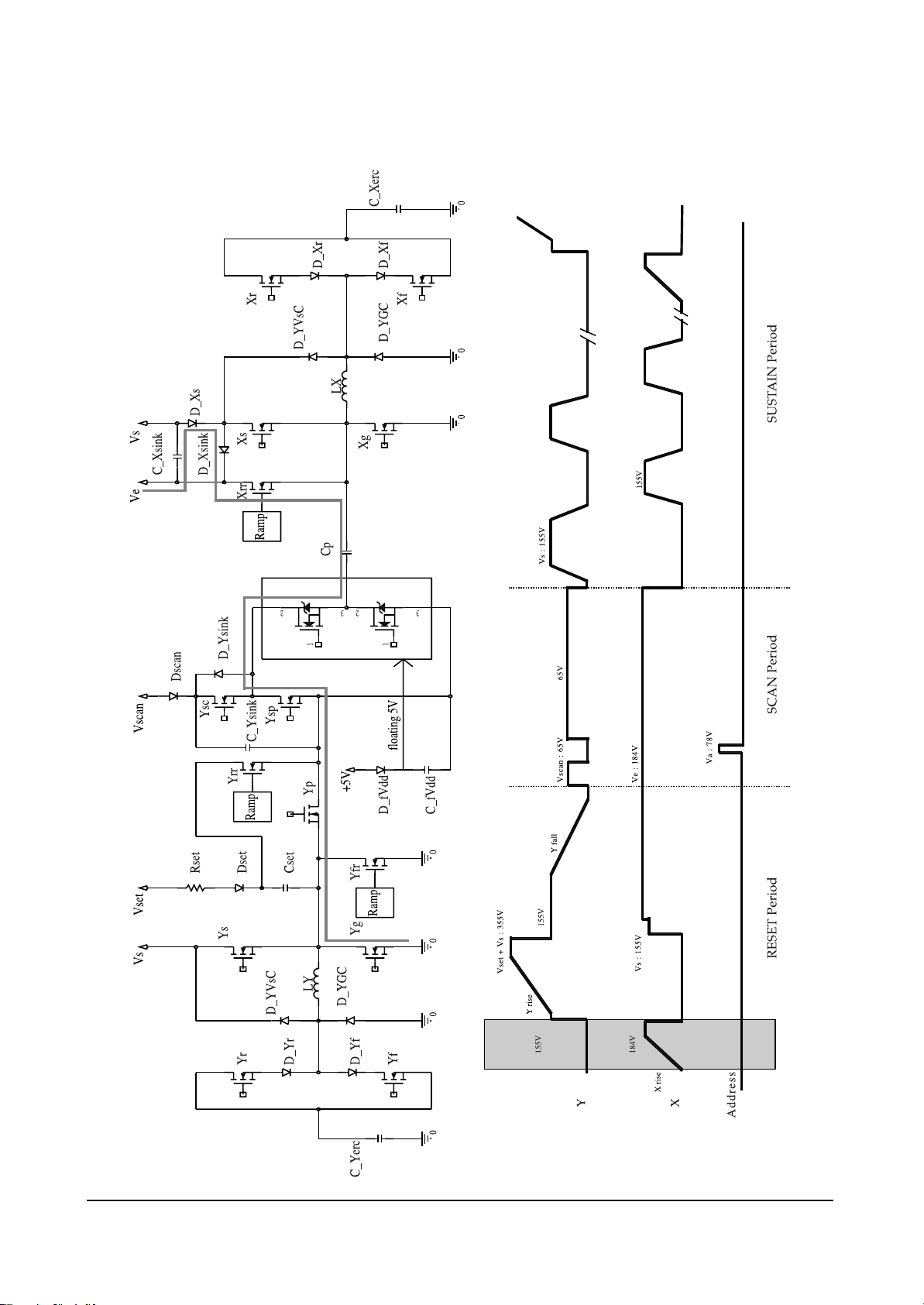
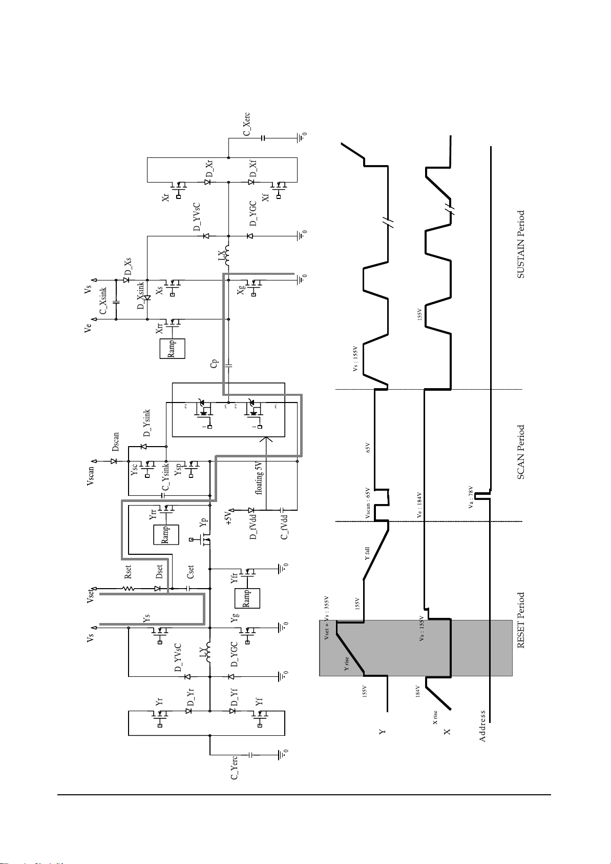
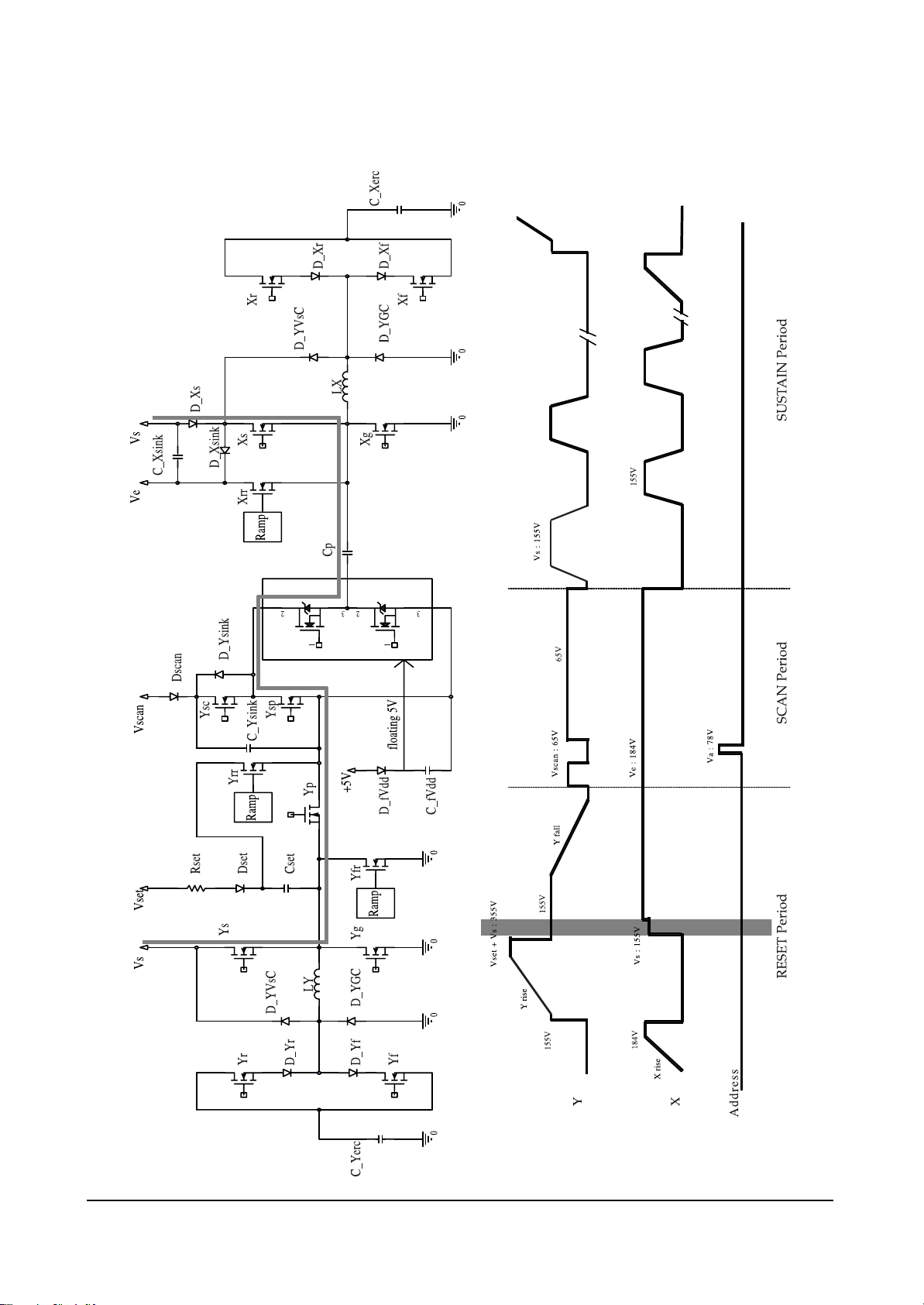
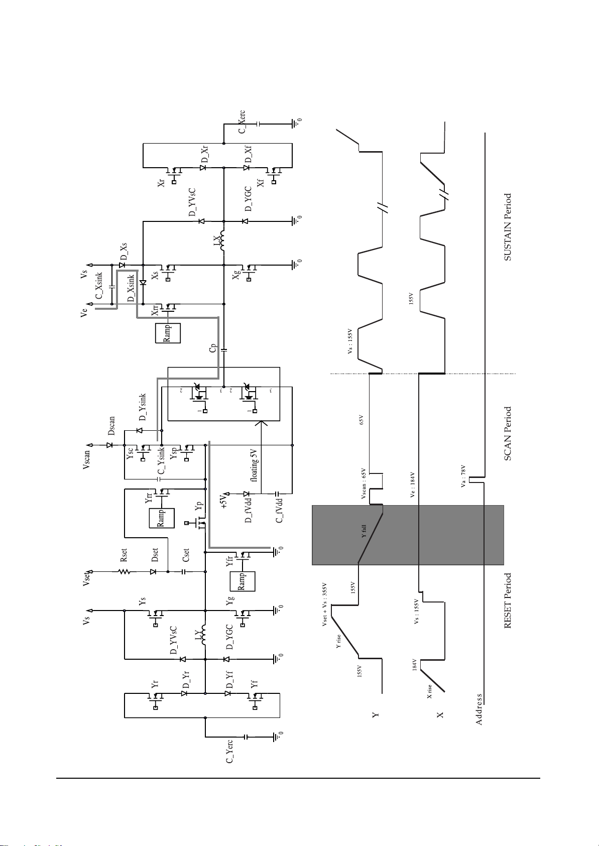
5-2-2 SPECIFICATION OF DRIVE PULSES
5-2-2(A) DRIVE PULSES
Page 11

Circuit Operation Description
Samsung Electronics 5-11
5-2-2(B) FUNCTIONS OF PULSES
(1) X rising ramp pulse
Just before X rising ramp pulse is impressed, the last Y electrode sustain pulse of previous sub field is
impressed. The pulse causes sustain discharge. Consequently, positive wall charge is accumulated in X
electrode, and negative wall charge is accumulated in Y electrode. X rising ramp erases wall charge
produced by the last sustain discharge pulse using weak-discharge.
(2) Y rising ramp pulse
During Y rising ramp period, weak-discharge begins when external voltage of about 390V~400V is
impressed to Y electrode, and each gap voltage is equal to discharge start voltage. Sustaining the
weak-discharge, positive wall charge is accumulated in X electrode and address electrode, and negative wall charge is accumulated in Y electrode of the entire panel.
(3) Y falling ramp pulse
During Y falling ramp period, the negative wall charge in Y electrode accumulated by 200V of X bias
is used to erase positive wall charge in X electrode. Address electrode (0V) sustains most of the positive electric charge accumulated during rising ramp period so that it can maintain wall charge distribution beneficial to the upcoming address discharge.
(4) Y scan pulse
This is called the scan pulse, selecting each of Y electrodes on a one-line-at-a-time basis. In this case,
Vscan means the scan bias voltage. About 70 V (Vscan) voltage is impressed on the selected electrode
lines, while 0 V (GND) voltage is impressed on the other lines.
In the cells the address pulse (70V~75V) is impressed on, address discharge is occurred because negative wall charge is accumulated in Y electrode, positive wall charge is accumulated in address electrode by the applied ramp pulse, and the sum of impressed voltage is greater than discharge start
voltage. Thus, because scan pulse and data pulse are impressed line by line, very long time is taken
for PDP addressing.
(5) 1st sustain pulse
The sustaining pulse always begins with the Y electrode. This is because when address discharge is
generated, positive wall voltage is generated on the Y electrodes. Because wall electric charge generated by address discharge is generally smaller than wall voltage generated by sustaining discharge, initial discharges have small discharge strength, and stabilization is usually obtained after 5~6 times discharges, subject to variations depending on the structure and environment of electrodes. The purpose
of impressing the initial sustaining pulses long is to obtain stable initial discharges and generate wall
electric charges as much as possible.
Page 12

5-2-3(A) FUNCTIONS OF EACH BOARD
(1) X board
X board is connected to the panel’s X-electrode blocks, 1) generates sustain voltage pulse (including
ERC), 2) generates X rising ramp pulse, and 3) sustains Ve bias during scan period.
(2) Y board
Y board is connected to the Y-electrode blocks of panel, 1) generates sustain voltage pulse (including
ERC), 2) generates Y rising and falling ramp pulse, and 3) sustains Vscan bias.
(3) Y buffer board (upper and lower)
Y buffer board impresses scan pulse to Y electrodes, and consists of upper and lower sub-boards. In
case of SD class, one board is equipped with 4 scan driver IC’s (STMicroelectronics STV7617 with 64
or 65 outputs).
(4) COF
Impresses Va pulse on address electrodes in the address section and generates address discharge
based on a difference between such Va pulse and scan pulse impressed on Y electrodes. It is in the
form of COF, and a COF is equipped with 4 data drive IC’s (STMicroelectronics STV7610A with 96
outputs). For a single scan, 7 COF’s are required.
Circuit Operation Description
5-12 Samsung Electronics
5-2-3 Configuration and Operation Principles of Driver Circuit
Y-Buffer (Upper)
Y Drive board
- Sustain pulse
(Energy recovery)
- Rising ramp pulse
- Falling ramp pulse
X Drive board
- Sustain pulse
(Energy recovery)
- Rising ramp pulse
- Ve bias
- Vscan pulse
Y-Buffer (Lower)
Y-electrode blocks
COF X-electrode blocks
(6 blocks)
(3 blocks)
Page 13

Circuit Operation Description
Samsung Electronics 5-13
5-2-3(B) DRIVING BOARD'S BLOCK DIAGRAM
(1) Y
(2) X
17V
170V
POWER
220V
75V
POWER
220V
17V
170V
Page 14

Circuit Operation Description
5-14 Samsung Electronics
➣ Components of driving board's operations
1. Power supply
1) Supplied from the power supply board
- For sustaining discharge: 180V;
- For logic signaling buffer: 5V; and
- For gate driver IC: 15V.
2) Generated by the internal DC/DC part
- For generating Vw pulse: 180V.
2. Logic signal
1) Supplied from the logic board
- Gate signals for FETs.
Page 15

Circuit Operation Description
Samsung Electronics 5-15
5-2-3(C) PRINCIPLES OF FET’S OPERATION AND HIGH VOLTAGE SWITCHIng
❏ FET’s operation principles
❏ FET’s high voltage switching principles
(1) With no signal impressed on G1, FET1 gets
open-circuited, and with signal impressed on
G2, FET2 gets short-circuited, thereby causing
GND to be outputted to output terminals.
(2) With signal impressed on G1, FET1 gets short-
circuited, and with no signal impressed on G2,
FET2 gets open-circuited, thereby causing
180V to be outputted to output terminals.
(1) With signal impressed on the gate (Positive voltage),
FET gets short-circuited (a conducting wire of zero (0)
resistance); and
(2) With no signal impressed on the gate (GND), FET gets
open-circuited (a non-conducting wire of ∞ resistance).
Page 16

Circuit Operation Description
5-16 Samsung Electronics
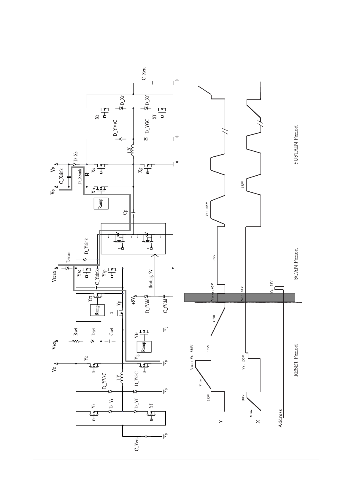
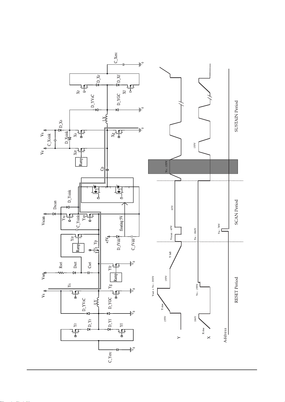
5-2-3 (D) DRIVER CIRCUIT DIAGRAM
Page 17

Circuit Operation Description
Samsung Electronics 5-17
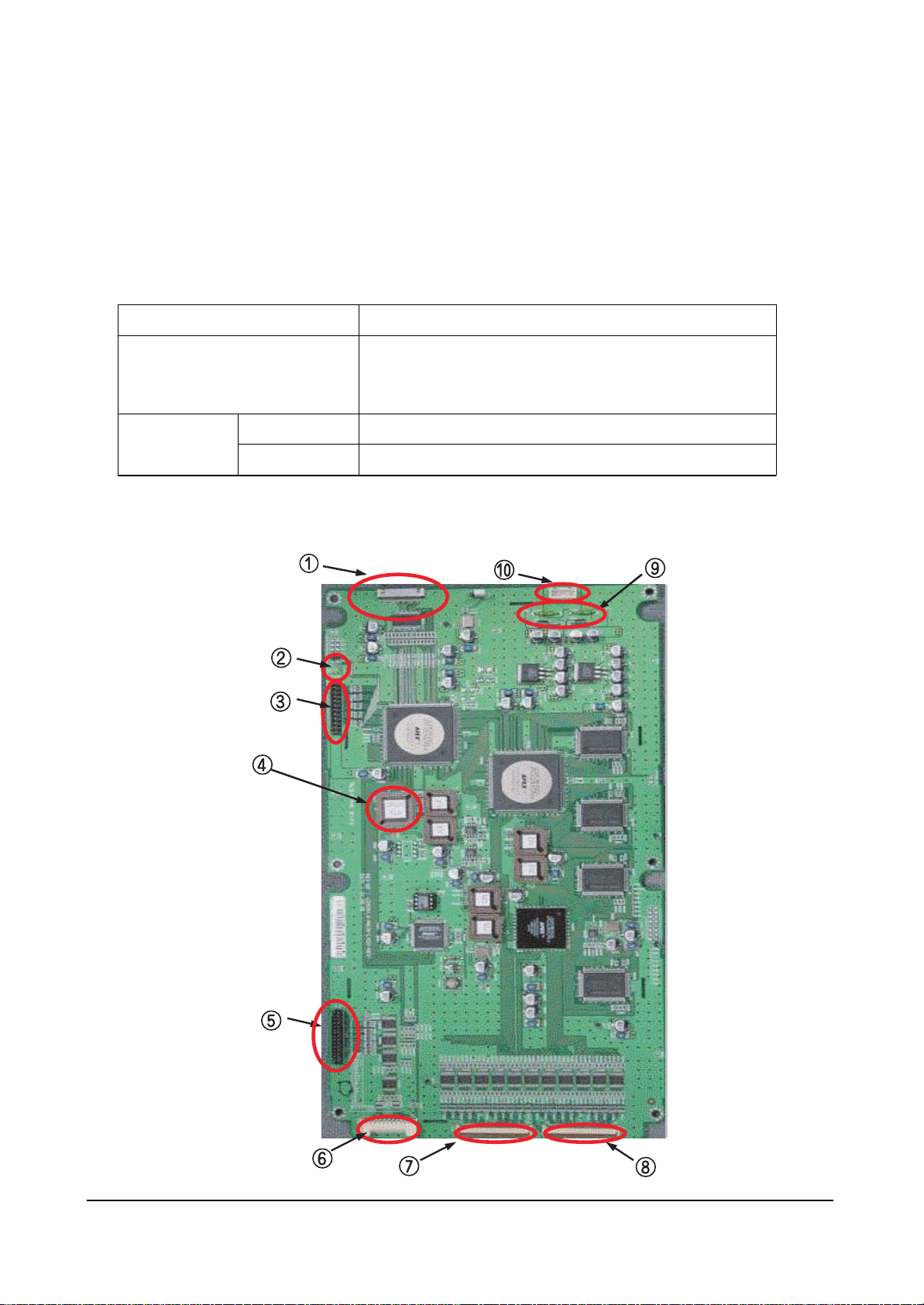
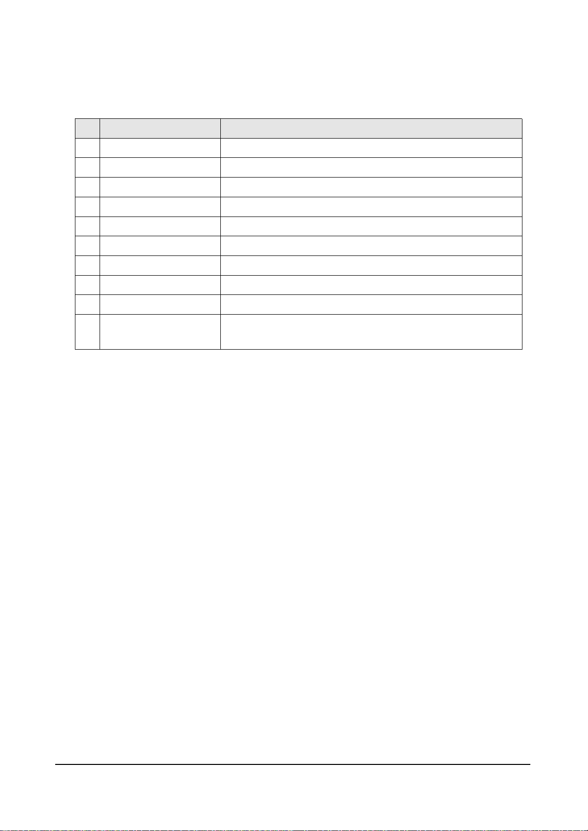
5-2-3(E) DRIVER BOARD CONNECTOR LAYOUT
Page 18

Circuit Operation Description
5-18 Samsung Electronics
Page 19
Circuit Operation Description
Samsung Electronics 5-19
Page 20
Circuit Operation Description
5-20 Samsung Electronics
Page 21
Circuit Operation Description
Samsung Electronics 5-21
Page 22

Circuit Operation Description
5-22 Samsung Electronics
Page 23
Circuit Operation Description
Samsung Electronics 5-23
Page 24
Circuit Operation Description
5-24 Samsung Electronics
Page 25

Circuit Operation Description
Samsung Electronics 5-25
Page 26

Circuit Operation Description
5-26 Samsung Electronics
Page 27

Circuit Operation Description
Samsung Electronics 5-27
Page 28

Circuit Operation Description
5-28 Samsung Electronics
Page 29
Circuit Operation Description
Samsung Electronics 5-29
Page 30

Circuit Operation Description
5-30 Samsung Electronics
Page 31

Circuit Operation Description
Samsung Electronics 5-31
5-3 Logic part
5-3-1 Logic Board Block diagram
Page 32
Circuit Operation Description
5-32 Samsung Electronics
5-3-1(A) TDESCRIPTION OF LOGIC BOARD
The logic board consists of the logic main board and the buffer board. The logic main board processes video
signal, generates, and output address driver output signal as well as XY drive signal. The buffer board
stores address driver output signal, and sends the signal to the address driver IC (COF module).
5-3-1 (B) NAME AND DESCRIPTION OF MAJOR COMPONENTS OF LOGIC BOARD
Logic Board
Login Main
Function
- Video signal processing (W/L, Error diffusion, APC)
- Outputs address drive control signal, and data signal to buffer board.
- Outputs XY drive board control signal.
Buffer board
E Buffer board
F Buffer board
Sends data and control signal to left-bottom COF
Sends data and control signal to right-bottom COF
Page 33
Circuit Operation Description
Samsung Electronics 5-33
5-3-1(C) WAVEFORMS IN NORMAL OPERATION
If the PDP unit and the logic board is in normal operation, the operation LED of Figure 1 would blink at
about 1 second interval.
If the unit is out of order, check the status of the operation LED through eye-inspection first. If the behavior
of the operation LED is different from that of normal state, you have to replace the board. To check trouble
on the board, the following logic board test procedures described below.
❑ 42°” SD s1.0 logic main board T/S
Required test equipment: : - Oscilloscope (digital 400 MHz 3 channel or more)
- Multi meter
Other equipment: : - DC power supply (5V: 1EA)
- Sub-PCB ASS'Y for JIG: 1 EA
Name
LVDS Connector
Operation LED
Key-Scan Connector
256k
Y Connector
X Connector
LE01 (Address Buffer Connector)
LE02 (Address Buffer Connector)
Power Fuse
Power Connector
No
1
2
3
4
5
6
7
8
9
10
Function
Input connector to receive encoded RGB, H, V, DATAEN, and DCLK signal.
It shows Sync and clock are properly received by the logic board.
Connector to connect key scan board to check and adjust 256K data.
EEPROM including gamma table, APC table, drive signal timing and other options
Connector to output Y drive board control signal
Connector to output X drive board control signal
Connector to output address data, and control signal to the E and F buffer boards.
Connector to output address data, and control signal to the E and F buffer boards.
Fuse connected to the power source line of the logic board.
Connector to connect the supply power (5V) with the logic board.
drive board control signal.
Page 34
Circuit Operation Description
5-34 Samsung Electronics
(1) First, perform eye-inspection and short circuit inspection for the power stage of the logic board to exam-
ine. Then, perform the following examinations on the board in order if no problem was found.
(2) Replace IC2017(256K EEPROM) of the logic board with Test EERPOM. Change the clock setting of the
logic board to internal referring to the configuration procedures described below.
❈ If there is no available Test EEPROM, you can use PG 00 for Windows NT systems, or PG 40 for
NT/PAL compatible systems by setting address 20 to 81, 22 to 00, 23 to 00,and 70 to 01.
(3) Connect power(5V) to LD1, and check that LED(LD2000) on the left top of the board blinks at about 1
second interval.
(4) If the logic board is out of order, the LED would blink too fast or not be lighted on.
(5) If no problem was found in the above examination, connect sub-PCB for logic output examination, mea-
sure output waveform, and compare the waveform with the appended waveform of normal state.
Record either OK or NG after examination.
(6) Check drive Y s/w, drive X s/w and address signal in order.
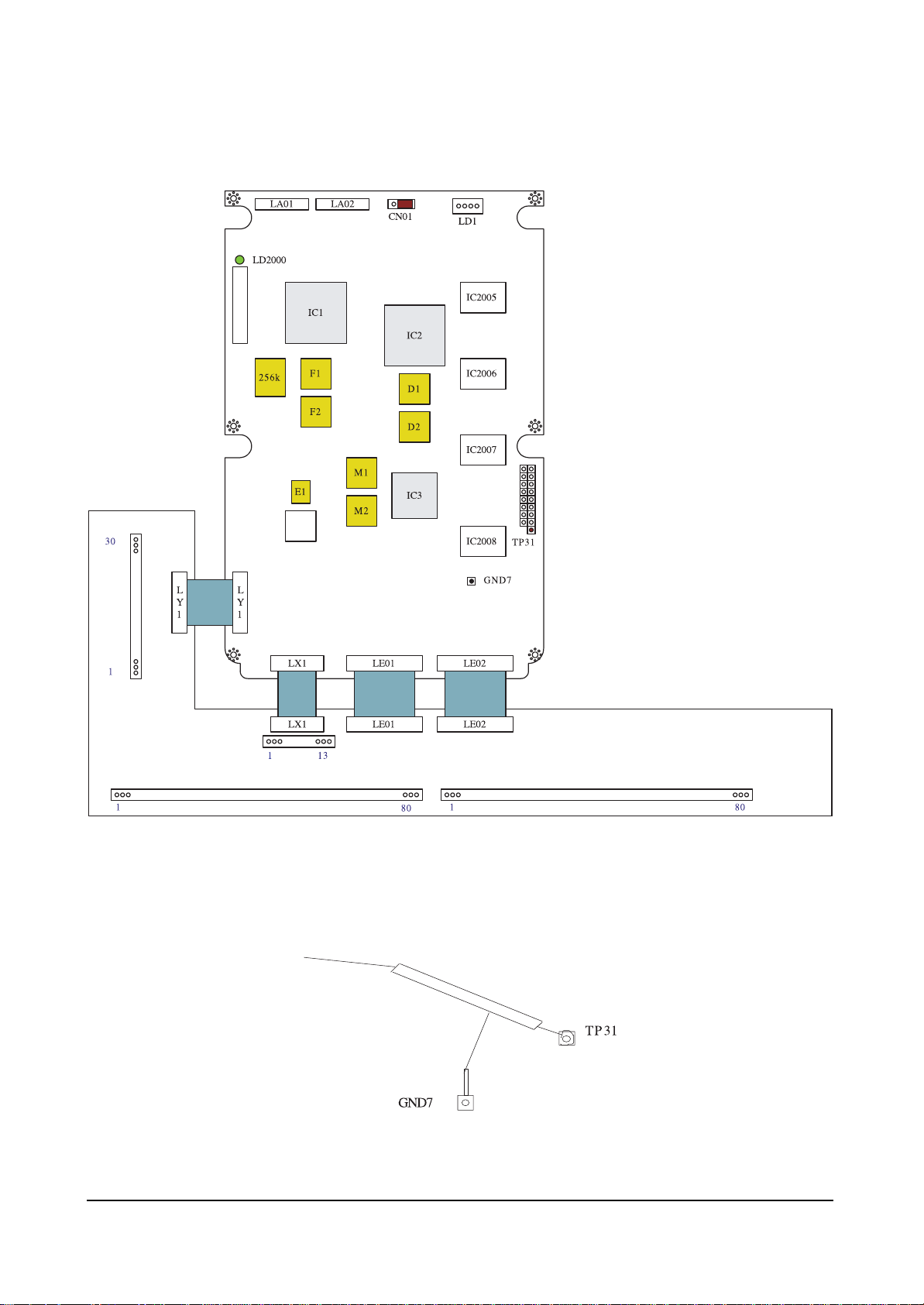
(7) Set probe 1 of oscilloscope to trigger signal, and connect it to the TP31 of the logic board.
(8) Set oscilloscope to 2ms/div. After adjusting probe 2 to 5V/div, check output signal.
(9) After T/S, turn off the power supply, and disconnect connector.
(10) Record the result on the examination sheet (either OK or NG).
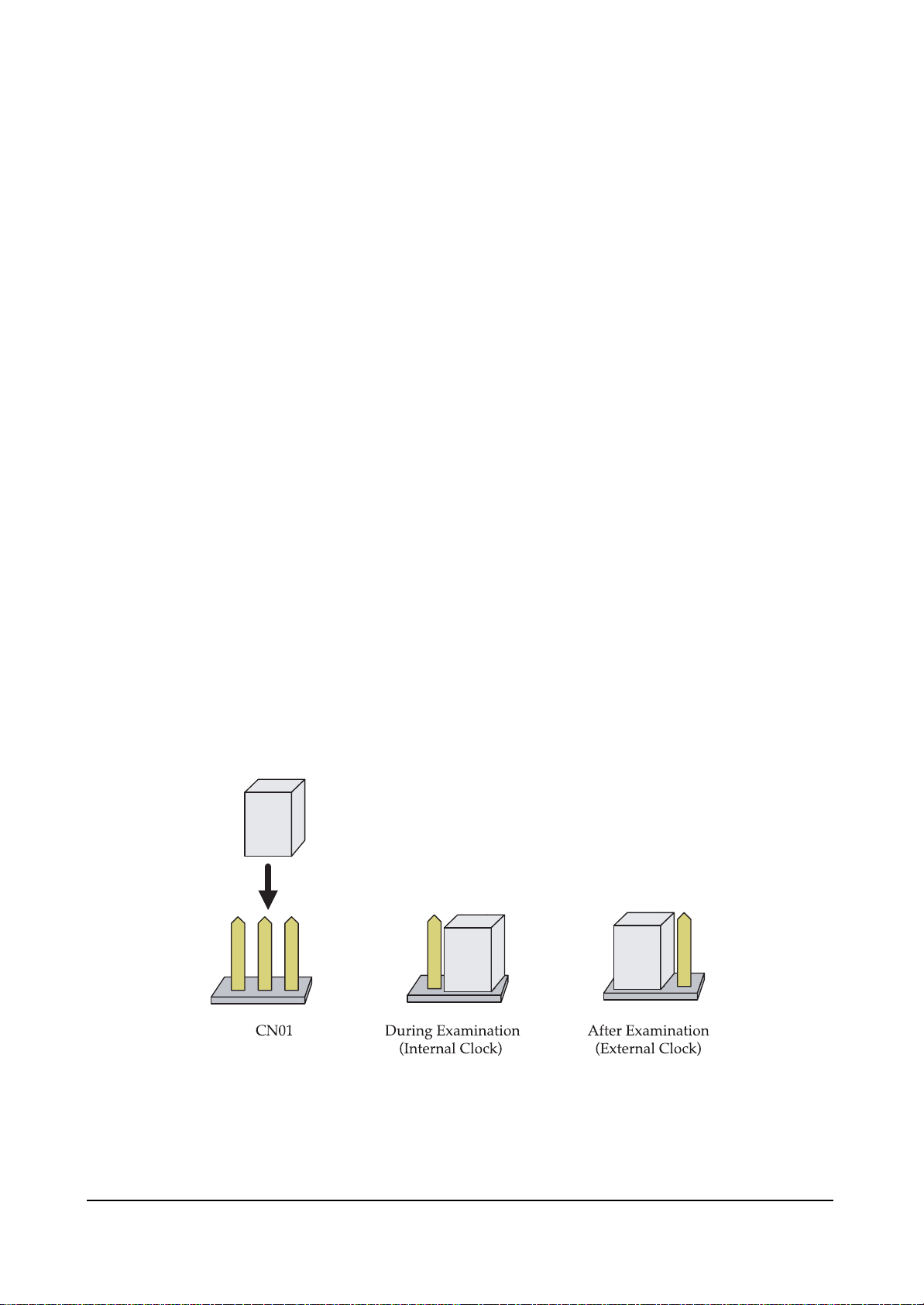
❐ Jumper settings to select internal or external clock
On the top of the logic main board, there is option jumper (CN01) that allows selecting internal/external
clock. While T/S, set it to internal clock as the following figure shows.
❈ It is set to external clock in normal. Set it to internal clock while examination, and set it to external
clock again after examination.
Figure 1. Jumper Settings to Select Internal / External Clock Signal
Page 35
Circuit Operation Description
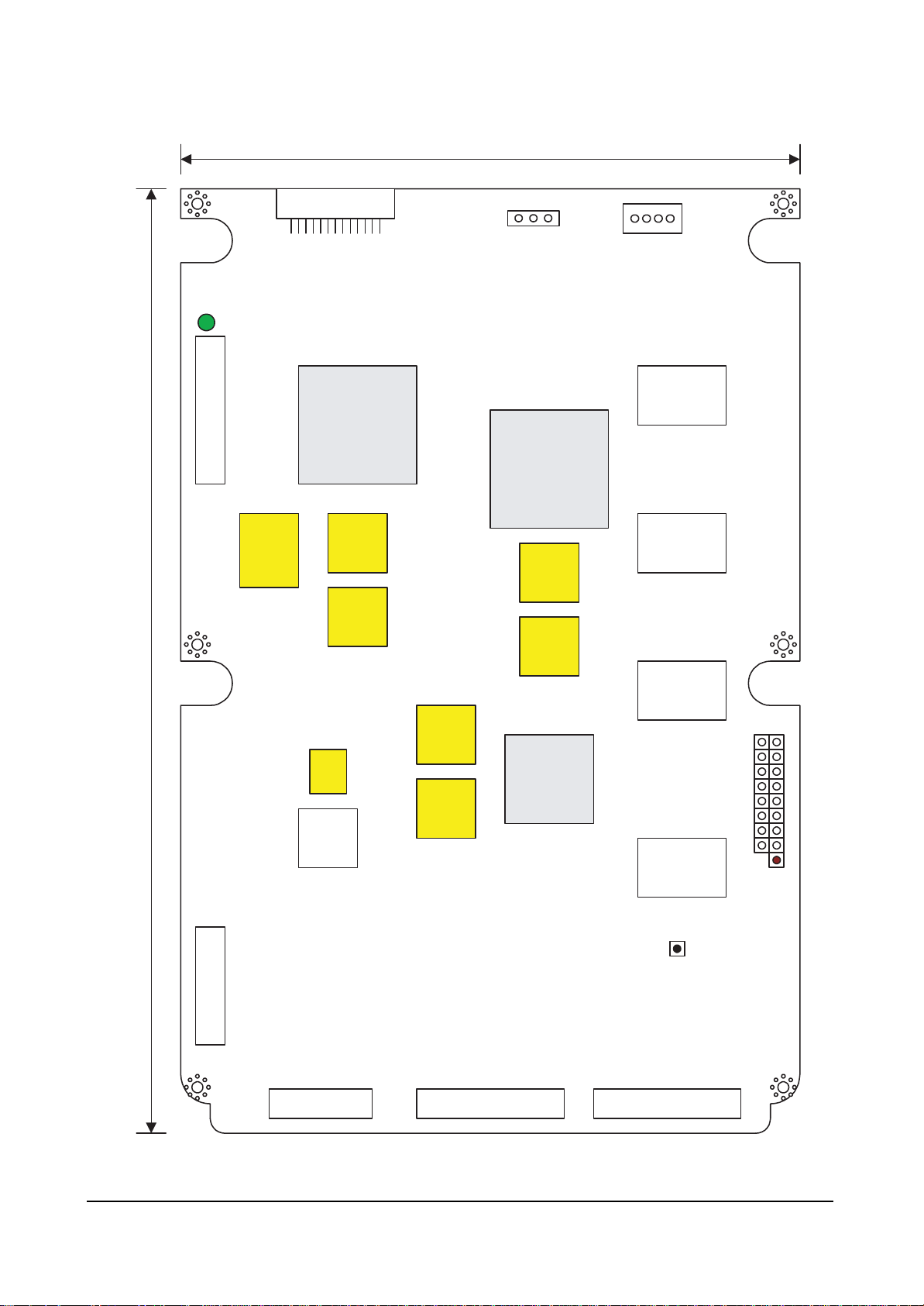
Samsung Electronics 5-35
LA03
Figure 2. Layout of 42" Signal Logic Main Board.
160mm
320mm
LD2000
256k
IC1
F1
F2
131
CN01
LD1
IC2
D1
D2
L
Y
1
M1
E1
IC3
M2
LX1 LE01 LE02
TP31
GND7
Page 36
Circuit Operation Description
5-36 Samsung Electronics
(1) Checking Y S /W
Figure 3. Connecting The Logic Main Board and The Test JIG Board
Figure 4. Connecting Oscilloscope Probe 1 (Trigger)
Page 37
Circuit Operation Description
Samsung Electronics 5-37
! Connect Probe 2 to LY1 30 of The JIG Board (8 (LE-Y) of The Logic Main Board F2016).
# Connect Probe 2 to LY1 25 of The JIG Board (6 (TCS_Y) of The Logic Main Board F2016).
@ Connect Probe 2 to LY1 28 of The JIG Board (7 (STB_Y) of The Logic Main Board F2016).
Page 38
Circuit Operation Description
5-38 Samsung Electronics
$ Connect Probe 2 to LY1 24 of The JIG Board (5 (CLK_Y) of The Logic Main Board F2016).
^ Connect Probe 2 to LY1 20 of The JIG Board (7 (SIA) of The Logic Main Board F2016).
% Connect Probe 2 to LY1 21 of The JIG Board (8 (SIB) of The Logic Main Board F2016).
Page 39
Circuit Operation Description
Samsung Electronics 5-39
& Connect Probe 2 to LY1 14 of The JIG Board (5 (YSP) of The Logic Main Board F2016).
* Connect Probe 2 to LY1 13 of The JIG Board (6 (YSC) of The Logic Main Board F2016).
( Connect Probe 2 to LY1 10 of The JIG Board (7 (YER) of The Logic Main Board F2016).
Page 40
Circuit Operation Description
5-40 Samsung Electronics
) Connect Probe 2 to LY1 9 of The JIG Board (8 (YP) of The Logic Main Board F2016).
1 Connect Probe 2 to LY1 8 of The JIG Board (6 (YRR) of The Logic Main Board F2016).
2 Connect Probe 2 to LY1 5 of The JIG Board (5 (YG) of The Logic Main Board F2016).
Page 41

Circuit Operation Description
Samsung Electronics 5-41
3 Connect Probe 2 to LY1 4 of The JIG Board (8 (YF) of The Logic Main Board F2016).
4 Connect Probe 2 to LY1 2 of The JIG Board (6 (YR) of The Logic Main Board F2016).
5 Connect Probe 2 to LY1 1 of The JIG Board (5 (YS) of The Logic Main Board F2016).
Page 42

Circuit Operation Description
5-42 Samsung Electronics
6 Connect Probe 2 to 1 and 72 of IC2005, and Check The Following Waveform Shows at Oscilloscope.
7 Connect Probe 2 to 1 and 72 of IC2006, and Check The Following Waveform Shows at Oscilloscope.
8 Connect Probe 2 to 1 and 81 of IC2007, and Check The Following Waveform Shows at Oscilloscope.
Page 43

Circuit Operation Description
Samsung Electronics 5-43
9 Connect Probe 2 to 1 and 81 of IC2008, and Check The Following Waveform Shows at Oscilloscope.
Page 44

Circuit Operation Description
5-44 Samsung Electronics
! Connect Probe 2 to LX1 2 of The JIG Board (6 (XRR) of The Logic Main Board F2016).
@ Connect Probe 2 to LX1 4 of The JIG Board (7 (XR) of The Logic Main Board F2016).
# Connect Probe 2 to LX1 6 of The JIG Board (8 (XS) of The Logic Main Board F2016).
(1) Checking X S /W
Page 45

Circuit Operation Description
Samsung Electronics 5-45
$ Connect Probe 2 to LX1 8 of The JIG Board (5 (XF) of The Logic Main Board F2016).
% Connect Probe 2 to LX1 10 of The JIG Board (6 (XG) of The Logic Main Board F2016).
Page 46

Circuit Operation Description
5-46 Samsung Electronics
■ 42°”SD logic buffer board T/S
Required test equipment : -.Oscilloscope (digital 400 MHz 2 channel or more)
Other equipment : -.DC power supply (5V : 1EA )
-.Multi meter
-.Logic board : 1EA
-.Sub-PCB ASS'Y for JIG: 1 EA
(1) First, perform eye-inspection and short circuit inspection for the power stage of the logic board to
examine. Then, perform the following examinations on the board in order if no problem was found.
(2) If no problem was found in step ®ÿ, connect buffer board as Figure 5 shows, connect sub-PCB for
COF data check and replace 256K EEPROM with Test EERPOM for the logic board to output fullwhite pattern.
(3) Supply 5V to the logic board, and check that the LED on the left-top of the board blinks at about 1 sec-
ond interval. If no problem is found, measure the output waveform of sub-PCB, and compare it with
that of normal state.
(4) Check EC1, EC2, EC3, EC4, FC5, FC6, and FC7 in order. You can only examine doubtable waveform
selectively.
(5) Set probe 1 of oscilloscope to trigger signal, and connect it to the TP31 of the logic board.
(6) Set oscilloscope to 2ms/div. After adjusting probe 2 to 5V/div, check output signal zooming important
points.
(7) Appended waveform is for full-white input pattern. Output waveform when each of R, G and B pat-
tern is supplied individually is summarized in the following table.
❈ For short check, it would be better to test waveform in the order of R, G and B pattern.
R0(TP13,TP49), R1(TP16,TP52), G0(TP14,TP50), G1(TP17,TP53),
B0(TP15,TP51), and B1(TP18,TP54) in The JIG Board
(8) After T/S, turn off the power supply, and disconnect the connector. Record the result on the examina-
tion sheet.
Output waveform for the applied pattern
Full-white R G B
The same as the attached waveform
Control signal output of
sub-PCB for COF data check
R, B, G data signal output of
sub-PCB for COF data check
The output waveforms of all of the
R, G, B TP’s are the
same as the
attached waveform.
The output waveforms of all of the
R0, R1 TP’s are the
same as the
attached waveform.
The output waveforms of all of the
G0, G1 TP’s are the
same as the
attached waveform.
The output waveforms of all of the
B0, B1 TP’s are the
same as the
attached waveform.
Page 47

Circuit Operation Description
Samsung Electronics 5-47
Figure 5. 42” Single logic buffer
Page 48

Circuit Operation Description
5-48 Samsung Electronics
! TP 13 ~ 18, 49 ~ 54 of The Test JIG Board
@ 21, 57 of The Test JIG Board
# 24, 31, 60, 67 of The Test JIG Board
(3) Checking buffer data
Page 49
Circuit Operation Description
Samsung Electronics 5-49
$ TP 25, 32, 61, 68 of The Test JIG Board
% TP 19, 26, 55, 62 of The Test JIG Board
^ TP 20, 27, 56, 63 of The Test JIG Board
Page 50
Circuit Operation Description
5-50 Samsung Electronics
5-4 Block Diagram
5-4-1 42” Monitor Scaler Block Diagram
IR
Key
LED
RE[7:0]
GE[7:0]
BE[7:0]
PROTECT
IR ,LED
Output CLK
DIS. OSC.
EEPROM
Key Matrix
)
hz
130M
(
)
Mh z
26
(
24C16
MCKE XT
<Image
DCKEXT
CLK2
I2C(1)
I2C
V_Y/ G V_Pr / R
DAC
SDA92 80
LVS
Pr ocess or >
Image Scaling
Pul se
Sandcast l e
SCP
H, V
V_Pb/ B
CXA2101AQ
RGB Matrix
LHS
LENG
DCL K
I2C
RTC
PCF8563
364
CPU
Wit h
OSD M i x e r
Frame Rat e
Conversi on
PW
V
G
Fl ash
Mem ory
29LV160
(CPLD)
VG[ 7: 0]
VR[ 7: 0]
VB[ 7: 0]
VHS
4A3
M
VCLK
SRAM
616V1000
KM
PLL
ADC
With
VS_OUT 1
AD9884
HS_OUT1
R, G, B_OUT,
SR[ 23: 0] , SQ[23: 0]
MHS, PCL K, SOG
CKI NV, CLAMP
MHSYNC, MCOAST
ADC
PLL
Wi t h
AD9 88 4
TXD/ RXD
YIN [ 7: 0]
UVI N[ 7: 0]
RCA OPTI ON
I2C
SDA94 00
Pr ogr essi ve
CLK2
Y [7: 0]
LLC1
UV [ 7 : ]
H1 _OUT
V1_OUT
I2C
Video
MAI N
CVBS, Y
Decoder
I VVS
IVHS
VPC3 230
YP r P b( DV D)
YPr Pb( DTV)
PIP
Video
CVBS
R, G, B, F B
Decoder
FI FO
VPC3 230
Y
DT V
Y
DVD
BA7657
PC_R. G. B.
SW
AX232A
Ser i al
M
SCART OPT I ON
CHSYNC
CVSYNC
PC_H, PC_V
or Audio
Sub P CB f
p.
Am
o
Au di
(TA1101)
C
o
2
429S )
I
7
Au di
Pr ocessor
(TDA
ADC
CVBS
eo
Vid
( CVBS)
MA IN_Y
MA IN_C
S1_DET
deo
(Y/C)
S-Vi
RCA
ponent
Input
Com
DVD VPC3230
( 480i )
DTV
t
Scar
PCF8591
I2C
nput
I
PC
#8 I D
(15pin D-SUB)
PC_R, PC_G, PC_B,
PC_H, PC_V
RS232C
( 9pi n,MALE)
n
I
o
3( L/R)
Au di
RS- 232
Page 51
Circuit Operation Description
Samsung Electronics 5-51
5-5 Major In/Out Signal Waveforms and Voltages of the Unit
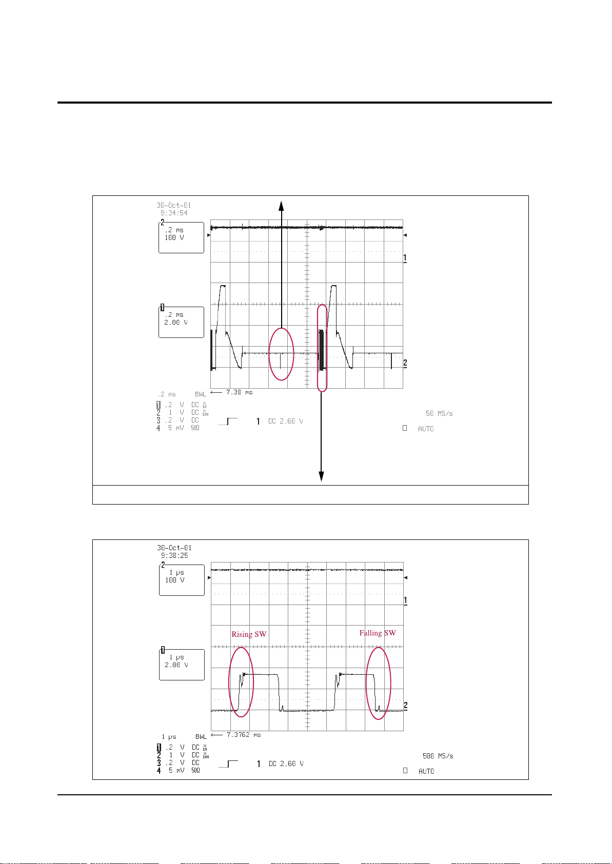
5-5-1 In/Out Waveforms
❏ Y output waveform
- It is the waveform when it is not connected to the panel.
* You should check that a single scan waveform is outputted!!!
Y output waveform (200us/div, 100V/div)
* You should check that energy recovery software is in operation!!!
Page 52
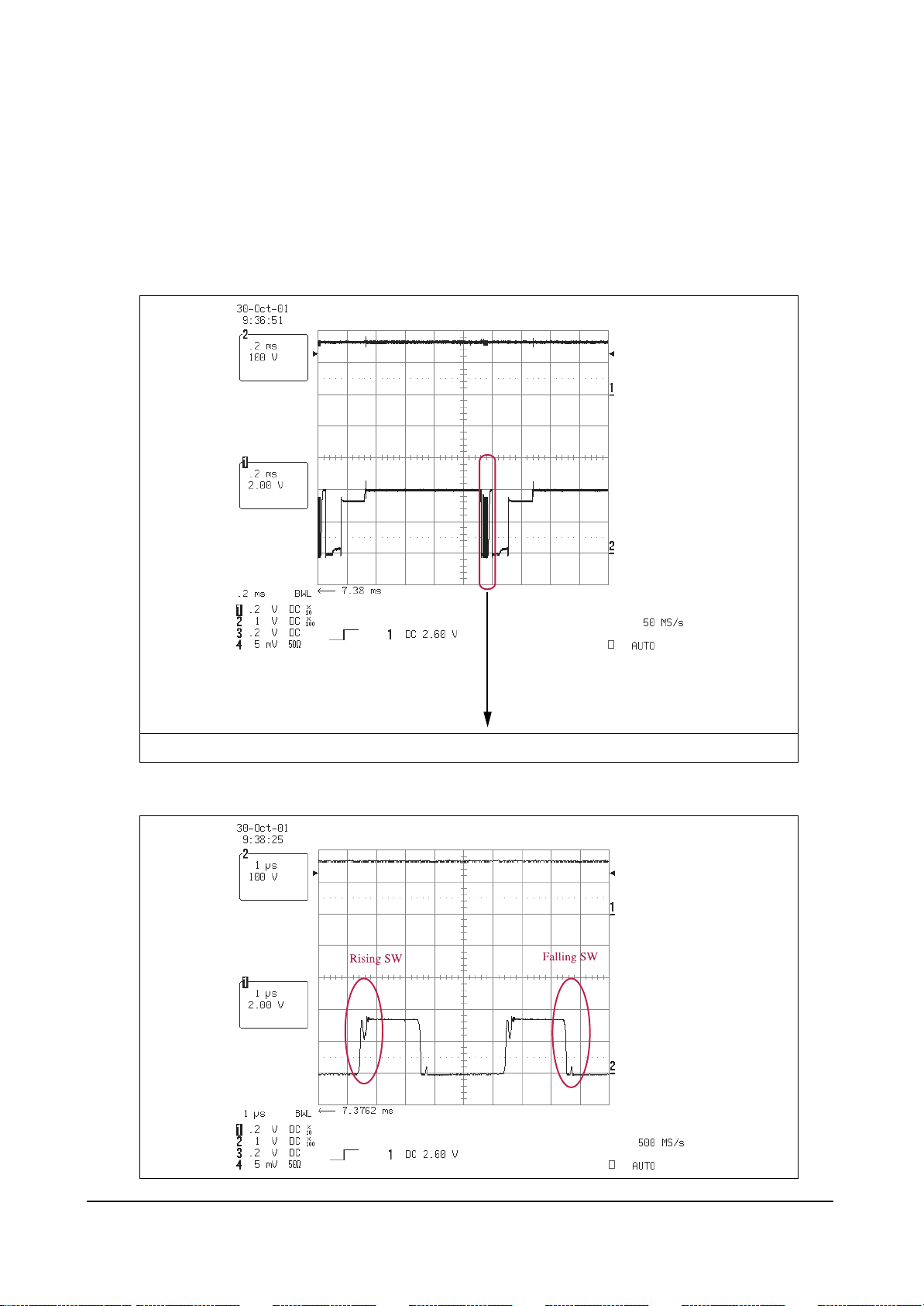
Circuit Operation Description
5-52 Samsung Electronics
❏ X output waveform
- It is the waveform when it is not connected to the panel.
X output waveform (200us/div, 100V/div)
* You should check that energy recovery software is in operation!!!
Page 53
Circuit Operation Description
Samsung Electronics 5-53
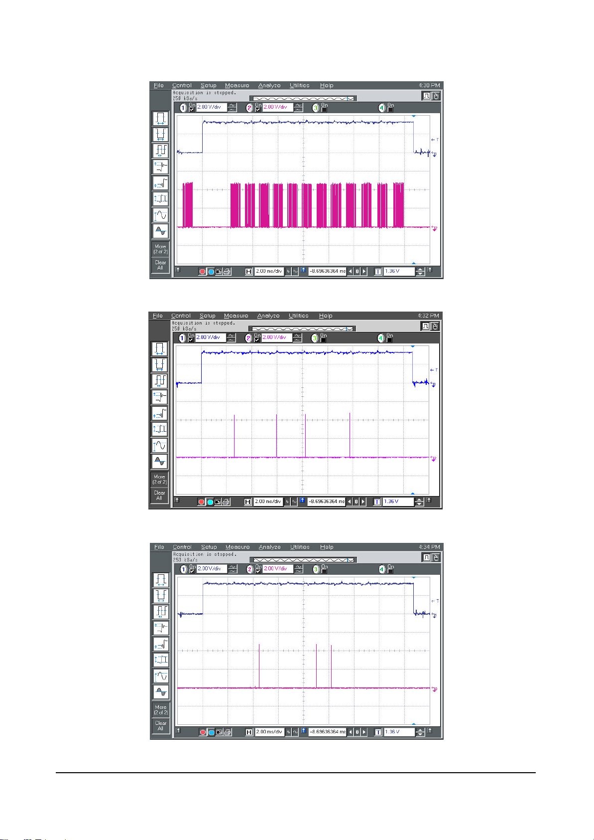
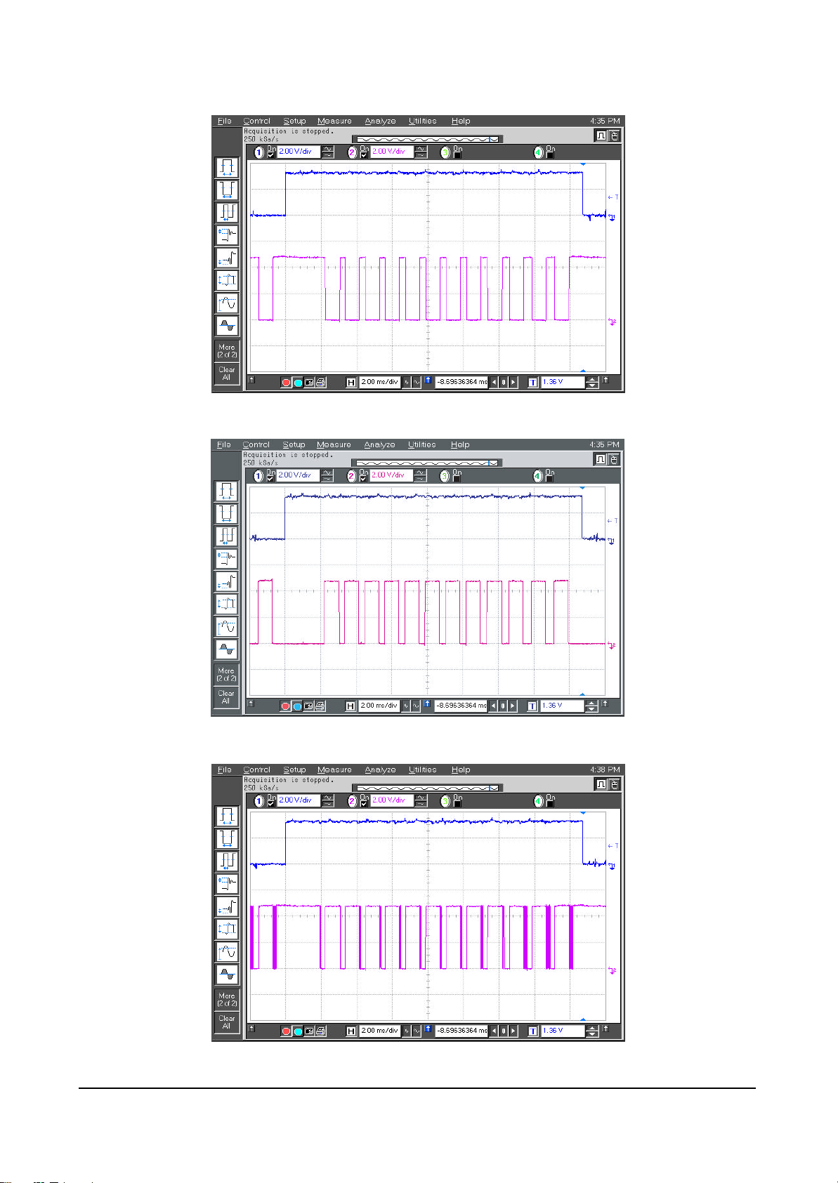
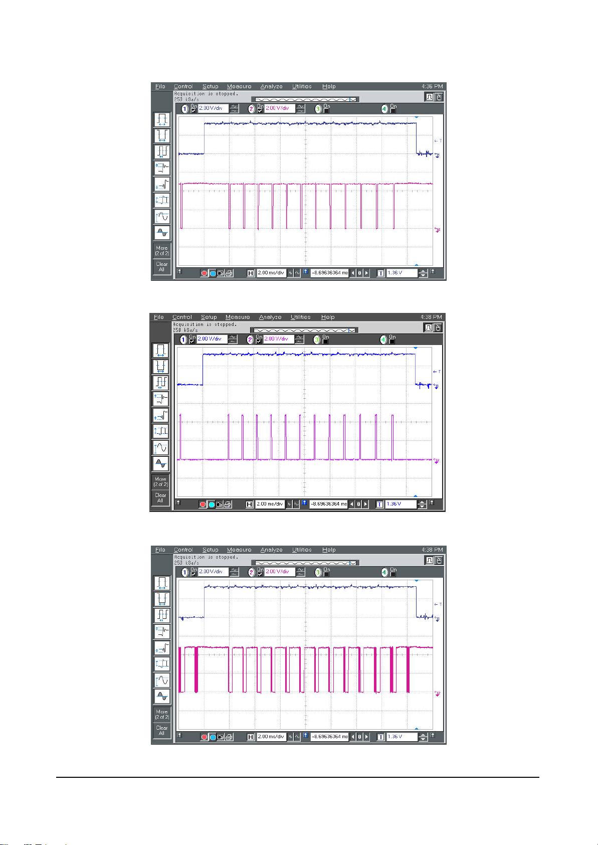
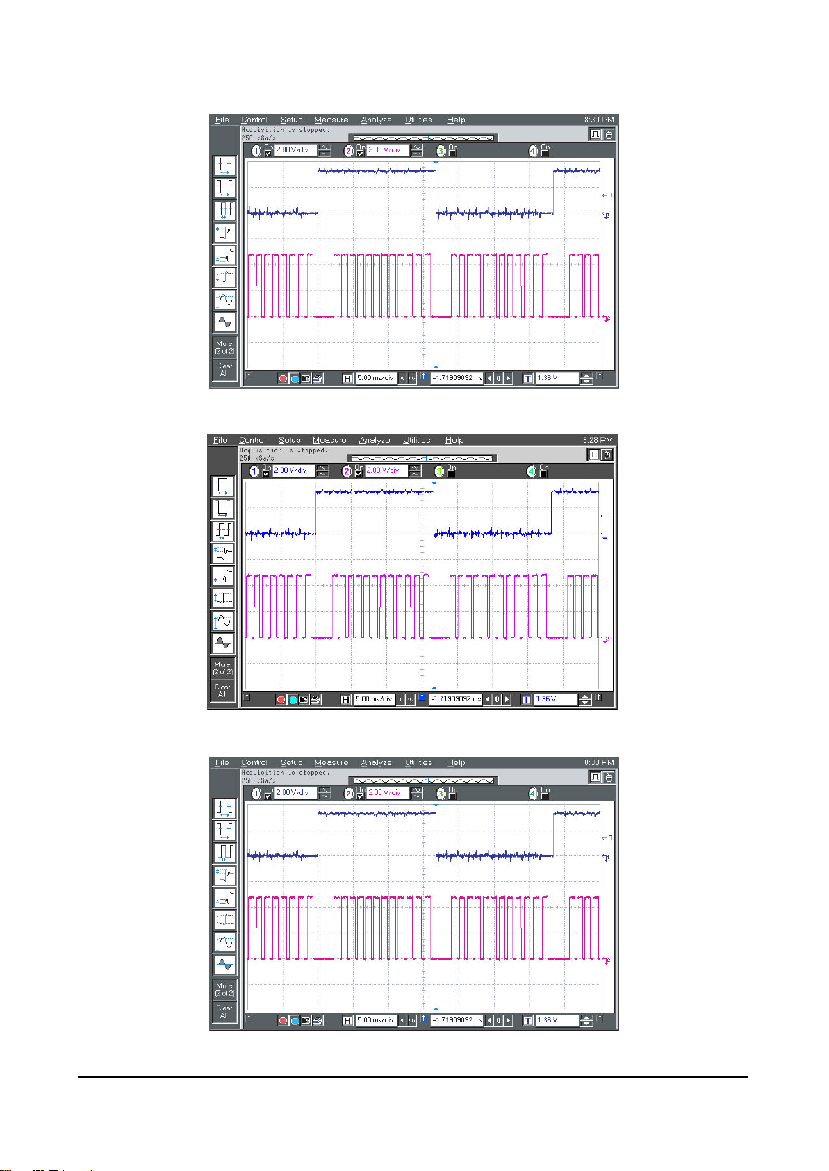
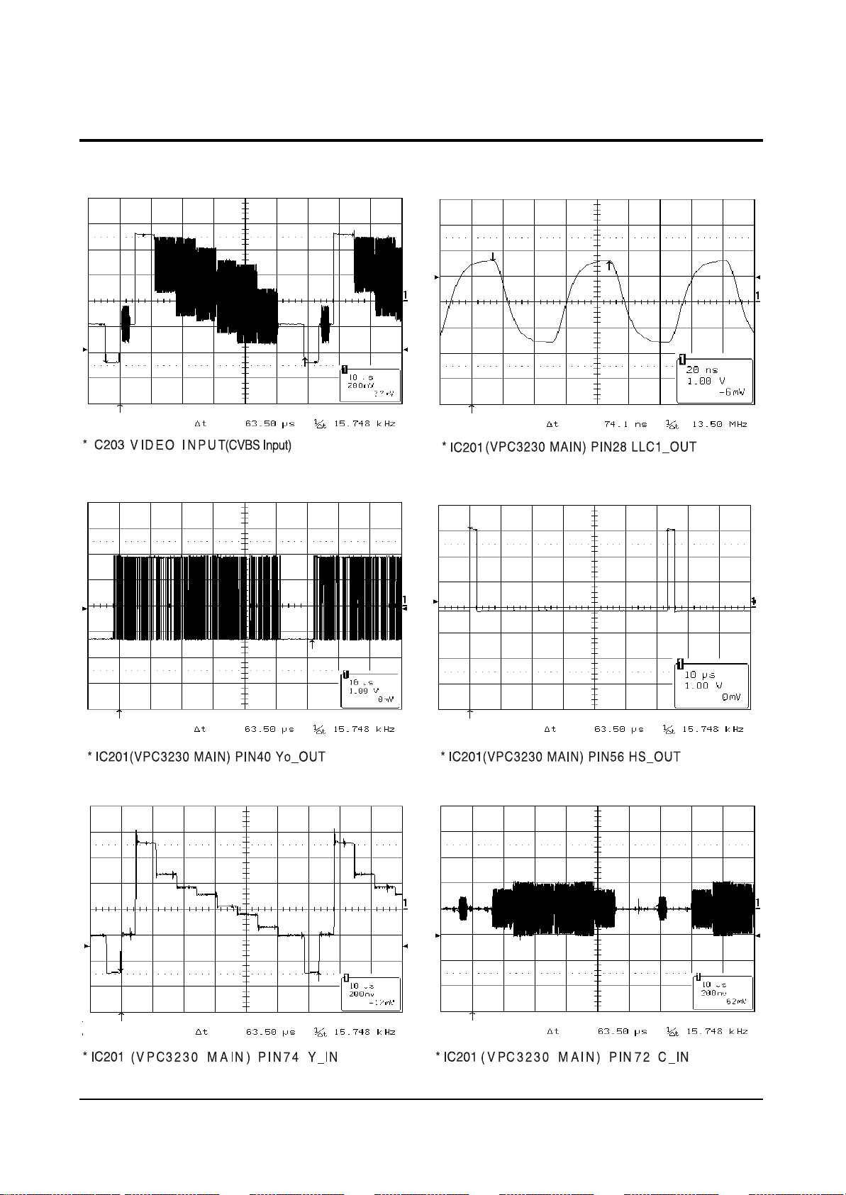
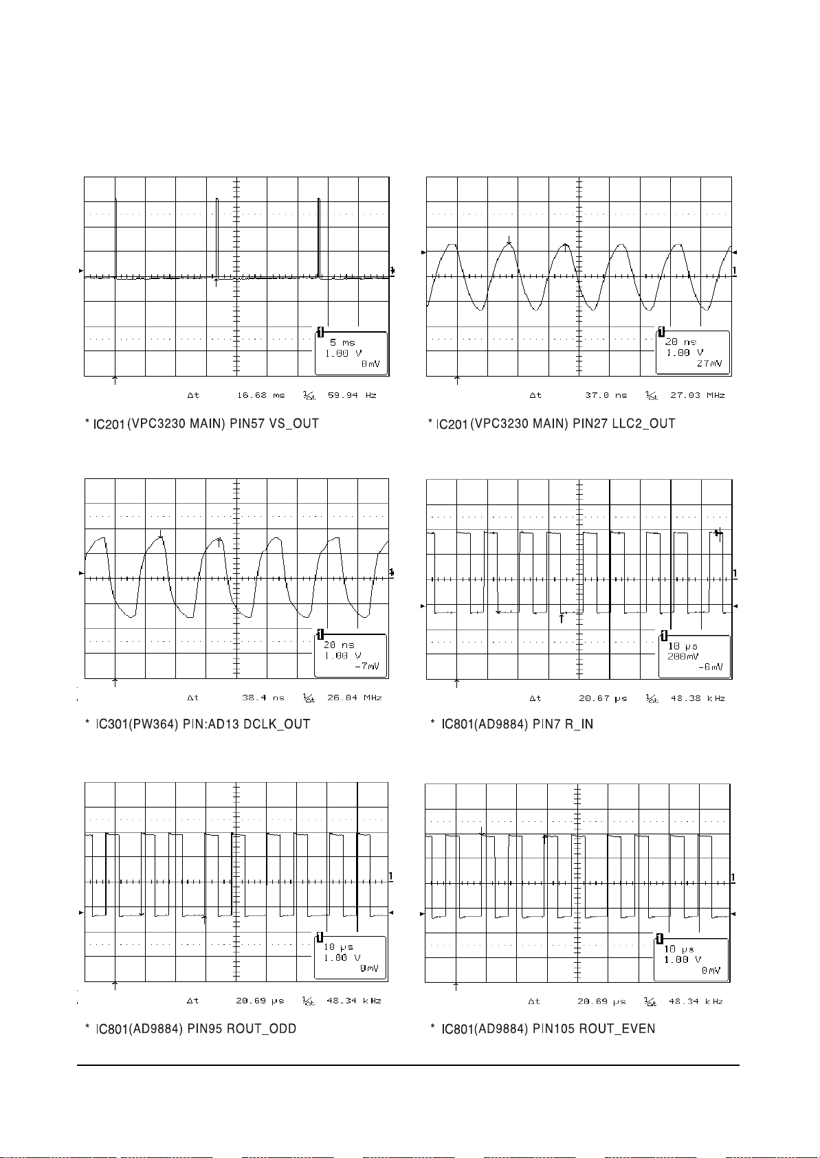
5-6 Main I/O signal pules and voltages
5-6-1 Signal Pulses of Image Board(Input Signal Conditions : 7 Color bar)
Page 54
Circuit Operation Description
5-54 Samsung Electronics
Page 55

Circuit Operation Description
Samsung Electronics 5-55
Page 56

5-56 Samsung Electronics
MEMO
Page 57

Circuit Operation Description
Samsung Electronics 5-57
 Loading...