

Page 1

PLASMA DISPLAY TV
Chassis : D65C(P)Asia
Model : PS42D4SX/RAD
PS42D4SX/XTT
PLASMA DISPLAY TV CONTENTS
Specifications
Alignment and Adjustments
Exploded View and Parts List
Service Item
Schematic Diagrams
1.
2.
3.
4.
5.
SERVICE
Manual
Page 2

ELECTRONICS
© Samsung Electronics Co., Ltd. Jul . 2004
Printed in Korea
AA82-01818A
This Service Manual is a property of Samsung Electronics Co.,Ltd.
Any unauthorized use of Manual can be punished under applicable
International and/or domestic law.
Page 3

Specifications
Samsung Electronics 1-1
1. Specifications
Page 4

1-2 Samsung Electronics
MEMO
Page 5

Alignment and Adjustments
Samsung Electronics 2-1
2. Alignment and Adjustments
2-1 Service Mode
2-1-1 SERVICE MODE Entry Method (General Transmitter)
¢ Using the Customer Remote
1. Turn the power off and set to stand-by mode.
2. Press the remote buttons in this order; POWER OFF-INFO-MENU-MUTE-POWER ON to turn the set on.
3. The set turns on and enters service mode.
¢ Using the Factory Remote
1. Turn the power on.
2. Press the remote buttons in this order : Display-Factory.
3. The set enters service mode.
* If you fail to enter service mode, repeat steps 1 and 2 above.
2-1-2 Initial SERVICE MODE DISPLAY State
2-1-2(A) OSD DISPLAY
2-1-2(B) Button Operations in SERVICE MODE
* While in Tuner mode, the direct access buttons can be used to select and change channels.
☞ Indicates selected input mode
☞ Picture Adjustment
☞ Setting the Initial Values
☞ Setting the Special Features
☞ Options-1 : Particulars Product Options
☞ Options-2 : PDP Properties Options
☞ Initializing after saving the adjustments
☞ Software Version Information
Factory Mode Current Input Mode
01. Picture Improvement ▶
02. Initial Setting ▶
03. PIP/TTX/Test Pattern ▶
04. Option-1 ▶
05. Option-2 ▶
06. Reset ▶
Release : 2004-05-19-15:30
Version : T-NELPEA-1017
Menu Displays all menus
UP/DOWN Cursor moves to select items
LEFT/RIGHT To increase and decrease the data of the selected items
(ENTER) Confirm your choice(Store OR Enter)
TV/VIDEO Button Change input source
Page 6

Alignment and Adjustments
2-2 Samsung Electronics
2-2 WHITE Balance Coordinates
2-2-1 PS42D4S White Balance Adjustment
1. W/B Adjustment is required for the following six modes :
DVI ’ Component(1080i) ’ Component(720p) ’ PC ’ VIDEO (Video port) ’ VIDEO (Graphic port)
2. Adjustment Method (Signal equipment : MSPG-925LTH, Measurement equipment : CA210)
■ MSPG-925LTH
Equipment that outputs analog and digital signals simultaneously
(Analog / Digital signal output / TV signal output (S-Video included) / HDTV signal output)
-. Digital Serial : TMDS (DVI24, SiI160) + DVI-I (Analog, Digital)
-. Monitor Signal (Analog): R, G, B, HS, VS, CS
-. TV Signal (CVBS) : NTSC M, NTSC J (7.5 IRE On/Off) (BNC or RCA), PAL B, D, G, H, I, PAL M, Nc
-. D-TV Signal (1080i, 720p, 480p)
♣
♣
MSPG-925 is used to adjust the W/B
■ CA210 : Color Analyzers adjusting brightness, chromaticity and etc.
-. R.G.B monochrome correction, brightness and gamma character adjustment
-. White Balance and flickering measurement
(1) Adjust the TV by varying the panel values and the video DNIe register in order th determine the reference W/B
with a DVI input.
(2) For Component mode, adjust the register of AD9883 to align the DTV signal to the DNIe and logic panel value .
(At this time, do not adjust the gain of AD9883 ’ the Highlight W/B does not need to be adjusted since its deviation falls within
valid distribution range.)
(3) PC adjustment is same as Component adjustment.
(The offset can be applied to the values obtained through DTV adjustment. However, additional adjustment is required for Y,
Cb, and Cr, since PC processes R, G, and B signals.)
* Attention for Component/PC adjustment
- Load the Auto color pattern. (Pattern #21)
♣
♣
Auto color pattern appears as black and white.
problems may occur if pattern #21 or similar
is not used.
- Excute factory mode auto color to adjust gain and offset.
- Load the Toshiba Pattern.(Pattern #16) and then adjust W/B.
♣
When factory mode auto color is executed, gain and
offset value is adjusted automatically.
Page 7

Alignment and Adjustments
Samsung Electronics 2-3
(4) Video adjustment should be performed with the Toshiba pattern in RF video mode.
The adjustment should be the same as in step 1.
Also, the video signal uses the video port when there is no other input signal. However, the signal uses the graphic
port in PIP mode, which includes other input signals (PC, DVI, Component, etc.), Video adjustment should be performed with
Video port and Graphic port separately.
* Thus, Micom saves the W/B data separately for each memory mode of the block (See the block diagram given below) during
W/B adjustment.
D
DTV
COMP1,2
RF
VIDEO
YPbPr
PC
(A-RGB)
DVI
(D-RGB)
V-PEAKING
RGB/YUV
CONTRAST
BRIGHT
TTX-mode
CXA2151
VPC3230
SIL169
RGB
Scaler
SW
RGB
IC
FLI2310
Y-Delay
C-Delay
Brightness
Contrast
Saturation
AD9883
Adjustment
Reg
Y/R-gain
Cr/B-gain
Cb/G-gain
Y/R-offset
Cr/b-offset
Cb/G-offset
Memory
Mode
Analog PC
- Auto Color
value(RGB)
DTV Mode
ASI510
Video
Port
RGB-cont
RGB-bri
R-gamma
G-gamma
B-gamma
Graphic
Port
DNIe
Adjustment
Reg
Bri-offset
Con-offset
Memory
Mode
- DVI
- PC
- Video
- Component(DTV)
Different adjustment values will be applied
to DVI, PC ,DTV(Component) and Video, mode.
DS90C385
Progressive
to
Interface
Logic
Adjustment
Reg
R-dri
G-dri
B-dri
R-cutoff
G-cutoff
B-cutoff
Memory
Mode
- DVI
- PC
- Video
- Component(
Page 8

Alignment and Adjustments
2-4 Samsung Electronics
2-3-1 Factory OSD Main Menu
2-3 Factory Data
☞ Indicates selected input mode
☞ Picture Adjustment
☞ Setting the Initial Values
☞ Setting the Special Features
☞ Setting PDP Properties Options
☞ Setting PDP Properties Options
☞ Initializing after saving the adjustments
☞ Software Version Information
01.Picture Improve
Factory Mode Current Input Mode
01. Picture Improvement ▶
02. Initial Setting ▶
03. PIP/TTX/Test Pattern ▶
04. Option-1 ▶
05. Option-2 ▶
06. Reset ▶
Release : 2004-05-19-15:30
Version : T-NELPEA-1017
☞ White Balance Adjustment
☞ Color Adjustment
☞ Contrast & Brightness Enhancement
☞ Detail Enhancement Sharpness Adjustment
☞ Y/C Delay Setting according to the System and
Input Modes
☞ Motion Enhancing Adjustment
☞ DNIe Registers
☞ Logic Registers of the Panel
☞ Picture Size Registers
01.Picture Improvement Current Input Mode
01. White Balance ▶
02. Color ▶
03. Cont/Bri Enhancement ▶
04. Detail Enhancement ▶
05. Y/C Delay ▶
06. Motion ▶
07. DNIe ▶
08. Logic ▶
09. Picture Size ▶
H/L
L/L
x
y
Y(fL)
x
y
Y(fL)
VIDEO
265
270
36
265
270
1.8
Component
260
270
38
260
270
0.5
PC
285
295
30
285
295
0.65
DVI
285
295
36
285
295
0.7
2-2-2 White Balance Coordinates by Mode(Southeast Asia)
Page 9

Alignment and Adjustments
Samsung Electronics 2-5
01.Picture Improve => 01.White Balance Adjustment
01.White Balance
01.R Drive
02.G Drive
03.B Drive
04.R Cutoff
05.G Cutoff
06.B Cutoff
07.Sub Contrast
08.Sub Brightness
09.R Gain
10.G Gain
11.B Gain
12.R/Cr Offset
13.G/Y Offset
14.B/Cb Offset
15.Auto color
TV
140
130
120
128
128
128
37
54
142
142
142
60
48
64
on/off
Mode-1
140
130
120
128
128
128
37
54
X
X
X
X
X
X
X
Initial Values of Input Modes
Video
Component PC DVI
Relevant IC
Logic
DNIe
AD9883
ITEM
♣ Input modes require respective storing the changes after adjustment.
01~06 : Logic
07~08 : DNIe
09~15 : AD9883
Mode-2
140
130
120
128
128
128
37
54
128
150
128
60
48
64
O
Mode-4
140
130
120
128
128
128
37
54
X
X
X
X
X
X
X
Mode-3
140
130
120
128
128
128
37
54
128
128
128
60
48
64
O
Page 10

Alignment and Adjustments
2-6 Samsung Electronics
01.Picture Improve => 02.Color Adjustment
02.Color
01.Saturation
02.Tint
03.RGB/YUV U-SAT
04.RGB/YUV V-SAT
05.RGB/YUV Tint
06.FLI-saturation
07.R Gamma
08.G Gamma
09.B Gamma
10.Gain-Sel
11.Cr Gain
12.Cb Gain
13.Y Gain
14. FLI-Y/G Bir
15. FLI-Cr/R Bir
16. FLI-Cb/B Bir
TV
129
32
35
37
0
130
30
30
30
1
7
7
1
0
9
7
Mode-1
129
32
35
37
0
130
30
30
30
x
x
x
x
0
9
7
Mode-2
x
x
x
x
x
x
32
32
32
1
7
7
1
x
x
x
Mode-3
x
x
x
x
x
x
32
32
32
x
x
x
x
x
x
x
Mode-4
x
x
x
x
x
x
32
32
32
x
x
x
x
x
x
x
Initial Values of Input Modes
PC DVI
Relevant IC
VPC3230
FLI2310
ASI510
CXA2151Q
FLI2310
ITEM
01 ~05 : VPC3230
07~09 : ASI510
06 : FLI2310
10~13 : CXA2151
14~16 : FLI2310
Video
Component
Page 11

Alignment and Adjustments
Samsung Electronics 2-7
01.Picture Improve => 03.Contrast & Brightness Enhancement
03.Cont/Bri Enhancement
01.Contrast
02.Brightness
03.RGB/YUV Contrast
04.RGB/YUV Brightness
05.FLI-Contrast
06.FLI-Brightness
07.R Contrast
08.G Contrast
09.B Contrast
10.R Brightness
11.G Brightness
12.B Brightness
TV
40
27
28
67
128
128
32
32
32
0
0
0
Mode-1
40
27
28
67
128
128
32
32
32
0
0
0
Mode-2
x
x
x
x
x
x
32
32
32
0
0
0
Mode-3
x
x
x
x
x
x
32
32
32
0
0
0
Mode-4
x
x
x
x
x
x
32
32
32
0
0
0
Initial Values of Input Modes
PC DVI
Relevant IC
VPC3230
FLI2310
ASI510
ITEM
01~04 : VPC3230
07~12 : ASI510
05~06 : FLI2310
Video
Component
Page 12

Alignment and Adjustments
2-8 Samsung Electronics
01.Picture Improve => 04.Detail Enhancement
04.Detail Enhancement
01.VAPGAIN
02.VAPINV
03.YPFT
04.YPFG
05.Peaking
06.Peaking Filter
07.Coring
08.HPLL_ERR_MIN
09.HPLL_ERR_MAX
10.V_SLICER
11.HenhGain
12.HLEGain
13.HChrEnGain
Mode-1
4
16
3
9
3
2
0
18
80
0
64
64
32
Mode-2
x
x
x
x
x
x
x
x
x
x
x
x
x
Mode-3
x
x
x
x
x
x
x
x
x
x
x
x
x
Mode-4
x
x
x
x
x
x
x
x
x
x
x
x
x
Initial Values of Input Modes
PC DVI
Relevant IC
uPD64083
VPC3230
FLi2310
ITEM
01~04 : uPD64083
05~10 : VPC3230
11~13 : FLI2310
Video
Component
4
16
3
9
3
2
0
18
80
0
64
64
32
TV
Page 13
Alignment and Adjustments
Samsung Electronics 2-9
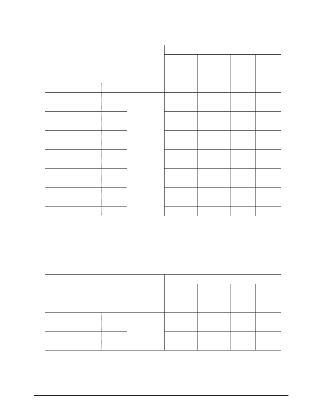
01.Picture Improve => 05.Y/C Delay Setting according to the System and Input Modes
05.Y/C Delay
01. PAL-B/G
02. PAL-D/K/L
03. PAL-I
04. SECAM-B/G
05. SECAM-D/K/L
06. NTSC
07. PAL-AV
08. SECAM-AV
09. NTSC-AV
10. RGB/YUV-Y
11. RGB/YUV-UV
12. FLI-Y
13. FLI-C
TV
255
254
254
251
250
254
254
252
254
90
90
5
11
Mode-1
255
254
254
251
250
254
254
252
254
0
0
5
11
Mode-2
x
x
x
x
x
x
x
x
x
x
x
x
x
Mode-3
x
x
x
x
x
x
x
x
x
x
x
x
x
Mode-4
x
x
x
x
x
x
x
x
x
x
x
x
x
Initial Values of Input Modes
PC DVI
Relevant IC
VPC3230
ITEM
01.Picture Improve => 06.Motion Enhancing Adjustment
06.Motion
01.HPLL Speed-1
02.Auto Lock
03.V-motion Tresh
TV
2
0
42
Mode-1
2
0
42
Mode-2
x
x
x
Mode-3
x
x
x
Mode-4
x
x
x
Initial Values of Input Modes
PC DVI
Relevant IC
VPC3230
FLi2310
ITEM
01~11 : VPC3230
12~13 : FLI2310
01 ~ 02 : VPC3230
03 : FLI2310
Video
Component
Video
Component
FLI2310
Page 14
Alignment and Adjustments
2-10 Samsung Electronics
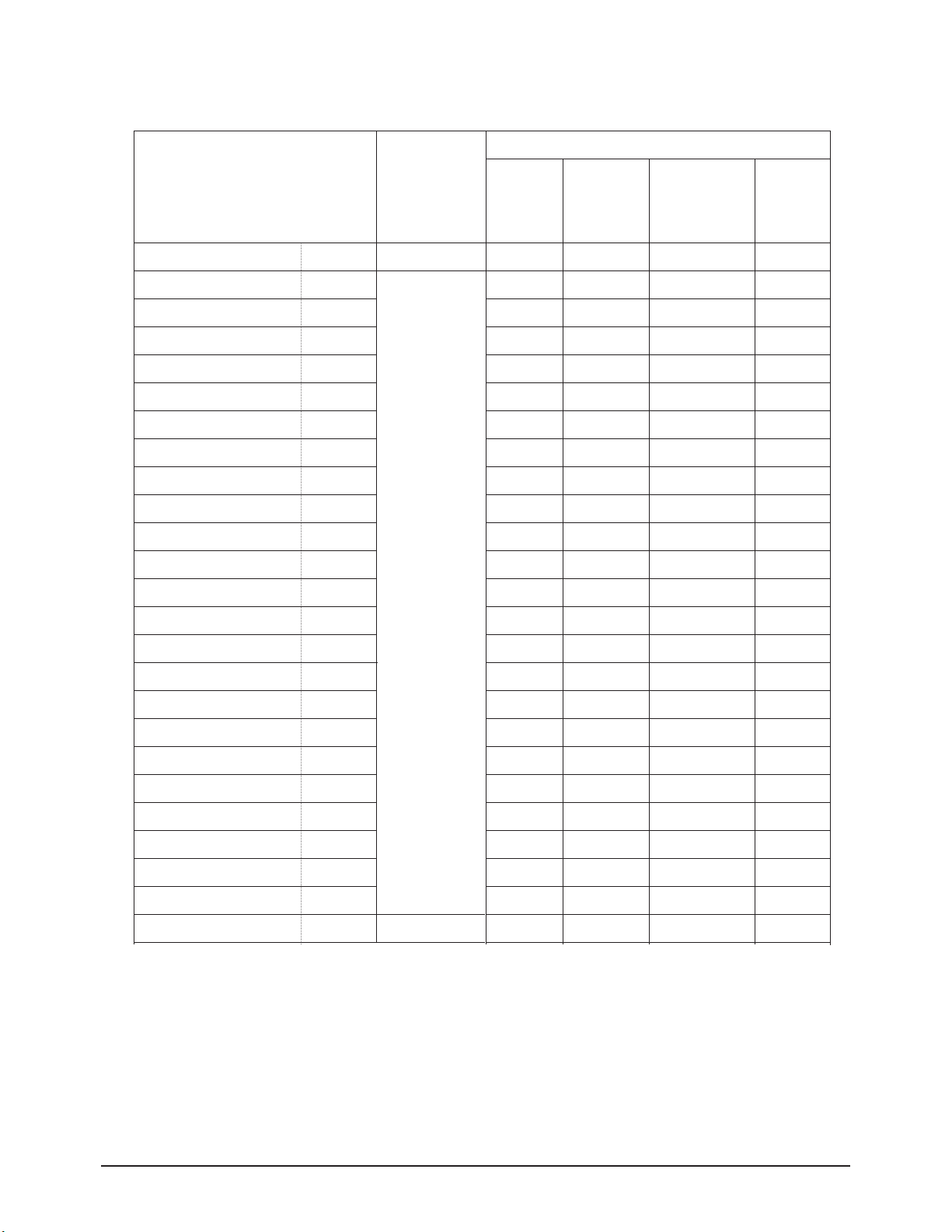
01.Picture Improve => 07.DNIe Registers
07.DNIe
01.SUB BRIGHT
02.SUB CONT
03.SCALE MAX
04.SCALE MIN
05.TH HPF
06.TH EDGE
07.NR SEL
08.CE UPPER
09.CE CUTOFF
10. CE GAIN
11. DCE GAIN
12. SKIN ON
13. CTI GAIN
14. DE NOISE GAIN
15. TH CORING
16. PATT SEL
17.DE NR
18. NOISE TH2
19. H CONT
20. V CONT
21. BLACK GAIN
22. WHITE GAIN
23. WTE GAIN
24. CTE GAIN
TV
54
37
48
16
0
4
2
240
32
64
75
0
0
8
3
0
1
100
63
63
2
31
300
176
Mode-1
54
37
48
16
0
4
2
220
32
64
75
0
0
8
3
0
1
100
63
32
11
31
300
176
Mode-2
54
37
48
16
0
4
2
200
32
80
75
0
0
8
3
0
1
100
63
63
6
31
300
176
Mode-3
54
37
48
16
0
4
2
240
32
64
75
0
0
8
3
0
1
100
63
63
2
31
300
176
Mode-4
54
37
48
16
0
4
2
240
32
64
75
0
0
8
3
0
1
100
63
63
2
31
300
176
Initial Values of Input Modes
PC DVI
Relevant IC
DNIe
ITEM
01~24 : DNIe
Video
Component
Page 15
Alignment and Adjustments
Samsung Electronics 2-11
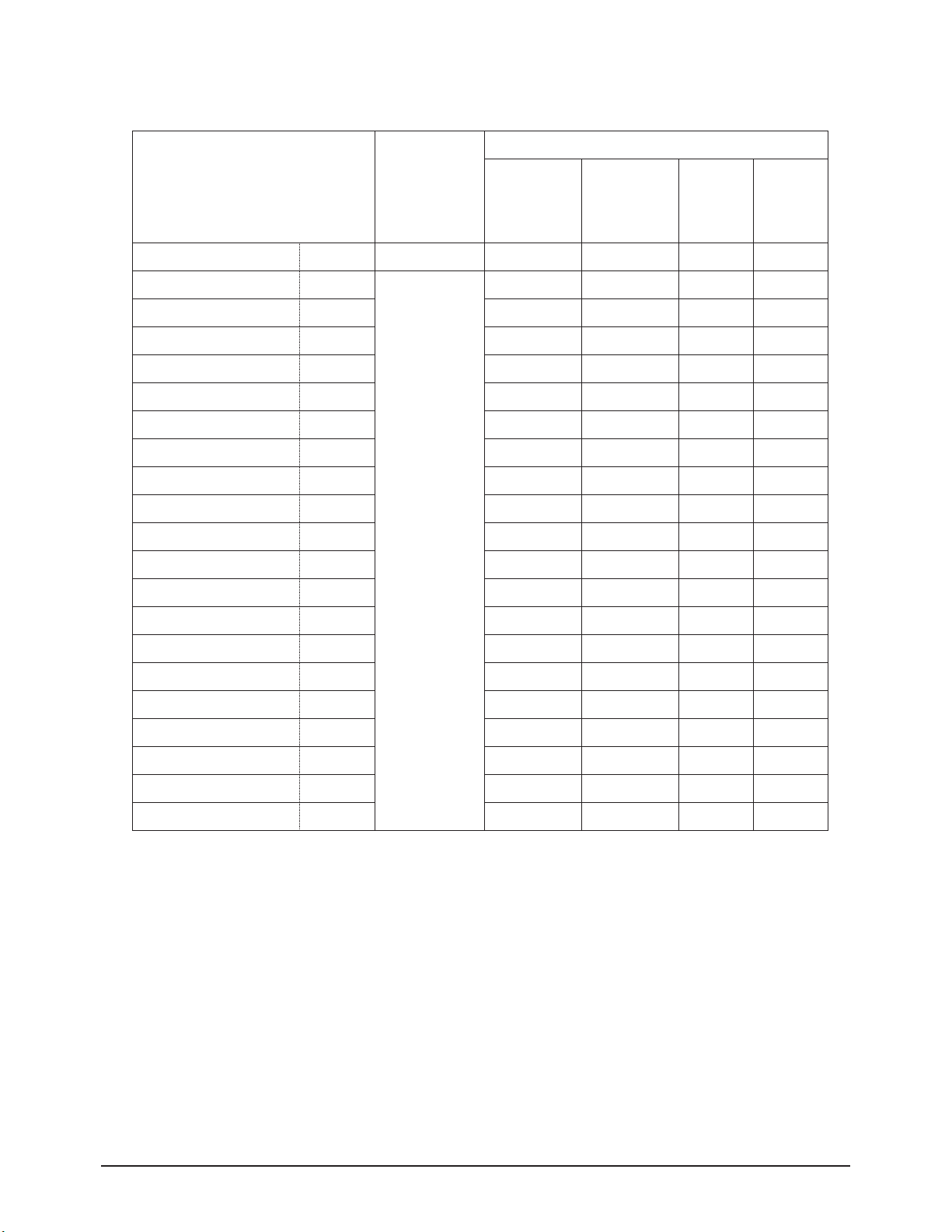
01.Picture Improve => 08.Logic Registers
08.Logic
01.R DRIVE
02.G DRIVE
03.B DRIVE
04.R CUTOFF
05.G CUTOFF
06.B CUTOFF
07.GAMMA
08.GTS SET
09.ERD MODE
10.RANDOM NOISE
11.DIFF FILTER
12.APC
13.APC SET
14.APC VALUE
15.ACTIVE VPOS
16.ACTIVE HPOS
17.VSYNC POS
18.HSYNC POS
19.VSYNC WIDTH
20.HSYNC WIDTH
TV
140
130
120
128
128
128
1
1
2
0
1
1
0
127
12
19
3
32
2
12
Mode-1
140
130
120
128
128
128
1
1
2
0
1
1
0
127
12
19
3
32
2
12
Mode-2
140
130
120
128
128
128
1
1
2
0
1
1
0
127
12
19
3
32
2
12
Mode-3
140
130
120
128
128
128
1
1
2
0
1
1
0
127
12
19
3
32
2
12
Mode-4
140
130
120
128
128
128
1
1
2
0
1
1
0
127
12
19
3
32
2
12
Initial Values of Input Modes
PC DVI
Relevant IC
Logic
ITEM
01~20 : Logic
Video
Component
Page 16
Alignment and Adjustments
2-12 Samsung Electronics
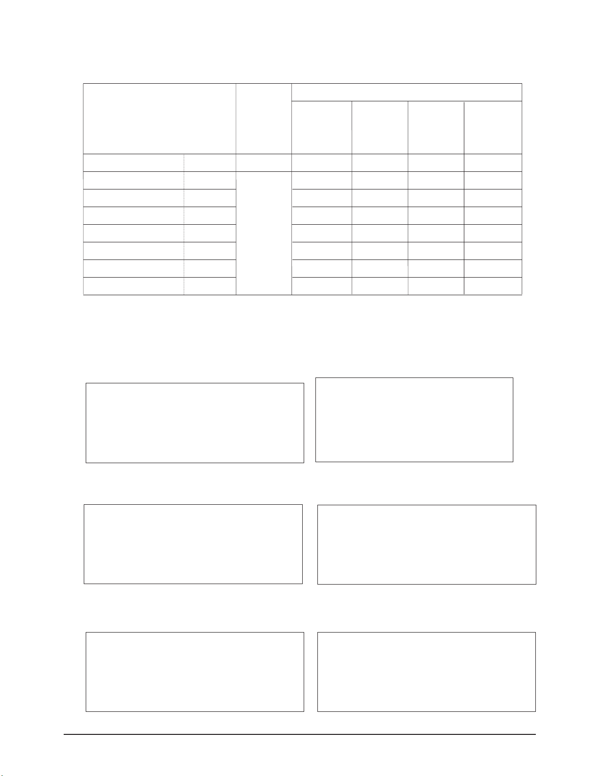
01.Picture Improve => 09.Picture Size Registers
09.Picture Size
01. H START OFFSET
02. V START OFFSET
03. H END OFFSET
04. V END OFFSET
05.OVERSCAN B
06.OVERSCAN G
07.OVERSCAN R
TV
0
0
0
0
38
38
38
Mode-1
0
0
0
0
38
38
38
Mode-2
0
0
0
0
38
38
38
Mode-3
0
0
0
0
38
38
38
Mode-4
0
0
0
0
38
38
38
Initial Values of Input Modes
PC DVI
Relevant IC
ASI510
ITEM
01~07 : ASI510
Video
Component
02.Initial Setting Current Input Mode
01. Initial P-Mode ▶
02. P-Mode Value ▶
03. Initial Color Tone ▶
04. Color Tone Value ▶
02.Setting the Initial Values
01.Initial P-Mode Current Input Mode
01. Dynamic
02. Standard
03. Movie
04. Custom
02.Initial Setting => 01.Initial P-Mode
02. P-Mode Value Current Input Mode
01. Dynamic ▶
02. Standard ▶
03. Movie ▶
04. Custom ▶
02.Initial Setting => 02.P-Mode Value
☞ Indicates selected input mode
☞ Reset after saving the P-Mode adjustments
☞ P-MODE the data Values
☞ Reset after saving the color tone adjustments
☞ Color tone the data Values
Available options for the PC/DVI Mode are High,Middle,
Low and Custom.
Available options for the PC/DVI Mode are High,Middle,
Low and Custom.
Page 17

Alignment and Adjustments
Samsung Electronics 2-13
02.Initial Setting Current Input Mode
01. Cool2
02. Cool1
03. Normal
04. Warm1
05. Warm2
♣ Available Settings for the PC Mode are
Custom,Color Tone 1, Color Tone 2, Color Tone 3
♣ Available options for the DVI Mode are
ColorTone1, ColorTone2, ColorTone3
02.Initial Setting => 03.Initial Color Tone
01.Dynamic Current Input Mode
01. Contrast ◀ 100 ▶
02. Brightness ◀ 45 ▶
03. Sharpness ◀ 75 ▶
04. Color ◀ 55 ▶
05. Tint ◀ 50 ▶
02.Initial Setting => 02.P-Mode Value => 01.Dynamic
02.Standard Current Input Mode
01. Contrast ◀ 80 ▶
02. Brightness ◀ 50 ▶
03. Sharpness ◀ 50 ▶
04. Color ◀ 50 ▶
05. Tint ◀ 50 ▶
02.Initial Setting => 02.P-Mode Value => 02.Standard
03.Movie Current Input Mode
01. Contrast ◀ 50 ▶
02. Brightness ◀ 55 ▶
03. Sharpness ◀ 25 ▶
04. Color ◀ 40 ▶
05. Tint ◀ 50 ▶
02.Initial Setting => 02.P-Mode Value => 03.Movie
04.Custom Current Input Mode
01. Contrast ◀ 80 ▶
02. Brightness ◀ 50 ▶
03. Sharpness ◀ 50 ▶
04. Color ◀ 50 ▶
05. Tint ◀ 50 ▶
02.Initial Setting => 02.P-Mode Value => 04.Custom
Page 18
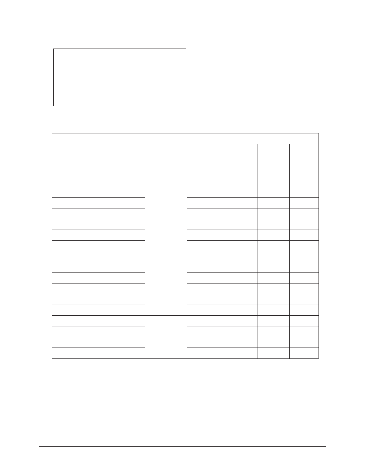
Alignment and Adjustments
2-14 Samsung Electronics
04.Color Tone Value Current Input Mode
01. Cool2
02. Cool1
03. Normal
04. Warm1
05. Warm2
♣ Adjusting and Storing the Changes:
Change the White Balance (Color Temperature)
1. Selecting an item will display the same options as
those of White Balance.
2. Available options for the PC Mode are Custom,Color
Tone 1, Color Tone 2, Color Tone 3
3. Available options for the DVI Mode are ColorTone1,
ColorTone2, ColorTone3.
4. Data Storing is classified according to the PC Mode &
Other Modes.
02.Initial Setting => 04.Color Tone Value
03.PIP/TTX/Test Pattern
03.PIP/Test Pattern
01.PIP R CONT
02.PIP G CONT
03.PIP B CONT
04.PIP R BRIGHT
05.PIP G BRIGHT
06.PIP B BRIGHT
07.PIP FILTER LC
08.PIP FILTER ML
09.PIP FILTER MR
10.PIP FILTER UC
11. TTX CONT
12. TTX BRIGHTNESS
13.LOG PATTERN
14.LOG HIGH LEVEL
15.LOG LOW LEVEL
16.ASI COLORBAR
TV
32
32
32
0
0
0
0
0
0
0
0
0
0
255
0
1
Mode-1
32
32
32
0
0
0
0
0
0
0
0
0
0
255
0
1
Mode-2
32
32
32
0
0
0
0
0
0
0
0
0
0
255
0
1
Mode-3
32
32
32
0
0
0
0
0
0
0
0
0
0
255
0
1
Mode-4
32
32
32
0
0
0
0
0
0
0
0
0
0
255
0
1
Initial Values of Input Modes
PC DVI
Relevant IC
ASI510
SDA6001
Logic
ASI510
ITEM
01~10 : ASI510
11~12 : SDA6001
13~16 : Logic, ASI510
Video
Component
Page 19

Alignment and Adjustments
Samsung Electronics 2-15
04.Option-1 Current Input Mode
00. AGC ◀OFF▶
01. TTX ON
02. CW/CS CS
03. TELE-WEB OFF
04. LANGUAGE GROUP ASIA
05. LANGUAGE ENGLISH
06. ATM OFF
07. Melody Volume 10
08. TUNER 1-TUNER
09. LNA ON
10. CHILD LOCK ON
11. TOP TTX OFF
12. TTX GROUP Osd Language
13. HIGH DEVIATION OFF
14. SD Delay 3
15. HD Delay 2
16. Video Port Graphic
17. DOC Write OFF
18. Initial Write OFF
04.Option-1
00. On => Off
02. CS(SOUTHASIA) => CW(EUROPE)
02. CW(EUROPE) => CS(SOUTHASIA)
03. Off => On
04. Asia => Europe
05. English => 5 Languages(Asia)
06. Off => On
07. 0 ~ 20
08. 1-TUNER
09. On => Off
10. On => Off
11. Off => On
12. Osd Language => 6 Group
13. Off => On
14. O(default),1(27ms),2(54ms),3(108ms)
15. O(default),1(27ms),2(54ms),3(108ms)
16. Graphic <-> Video
17. OFF->ON
18. OFF->ON
00. AGC : ON <-> OFF
-. OFF : VSP9437,(Master)0x0Bh[b7.b6]=[11], (Slave)0x6Fh[b7.b6]=[11]
-. OFF : VSP9437,(Master)0x0Bh[b7.b6]=[00], (Slave)0x6Fh[b7.b6]=[00]
01.TTX
-. ON : TTX Function it operates
- OFF : TTX Function it does not operate
02. CW/CS : CW => CS
- CW : PAL, SECAM-B/G, D/K, I, L/L', NTSC4.43 = West Europe
- CS : PAL, SECAM-B/G, D/K, I, NTSC3.58/4.43 = Countries except West Europe.
Ex) Southeast Asia,the Middle East,Russia,China, etc.
03. Tele-Web
- Off : TeleWeb non-broadcasting Country
- On : TeleWeb broadcasting Country
04. Language Group : Europe => Asia
-. Europe : 18 languages
-. Asia : 7 languages
05. Language : Select language
- Language Group is Europe : 18 languages
(English=>Bulgarian=>Croatian=>Czechoslovak=>Netherlandish=>French=>German=>Greek=>Hungarian=>
Italian=>Poland=>Portuguese=>Rumanian=>Russian=>Spanish=>Swedish=>Turki=>Yugoslave)
- Language Group is Asia : 5 languages
(English=>French=>Chinese=>Arabic=>Persian)
06. ATM : On => Off
-. ATM available region : On
-. ATM non-available region : Off
-. ATM at the time of OFF one from Funtion item the Country is changed with the Area and the ATM is changed with auto
search.
Page 20

Alignment and Adjustments
2-16 Samsung Electronics
07. Melody Volume
-.Able to adjust from 0 to 20.
08. Tuner
-. 1-Tuner
09. LNA
- On : Using LNA built-in Tuner
- Off : Not in use LNA built-in Tuner
10. Child Lock
-. On : TV Model
-. Off : Model has deletion of Child Lock function
11. Top TTX
- On : Only Top broadcasting region set 'On'
Ex) Germany, Switzerland, etc
- Off : Country except Top broadcasting region.
12. TTX Group : TTX Language Group and National Option Code
- By language, Select at the factory option table.
- TTX language will be displayed by National Option code.
- TTX Language Group by each country : 6 Groups
West Europe => East Europe => Turkish/Greek => Cyrillic => Arabic/Hebrew => Farsi/Hebrew => Osd Language
13. High Deviation : To prevent Sound Buzz resulting from regional conditions of the input signals.
- Set to ‘Off’ for the standardized sound input signal, in the region such as Europe.
- Set to ‘On’ for the over-modulated sound input signal, in the region such as Southeast Asia.
14. SD Delay : AV mode Delay
1.8ms delay --------- delay0
27ms delay --------- delay1
54ms delay --------- delay2
108ms delay (max) --------- delay3
15. HD Delay : DTV/PC/DVI mode Delay
16. Video Port : Setting of Aurora Input Port for VIDEO signal
-. Graphic : Input Video Signal though Graphic port of Aurora (In case of NON-PIP VIDEO)
-. Video : Input Video Signal though Graphic port of Aurora (In case of PIP VIDEO)
17. DDC Write
-.Off : Disable to write DVI DDC (DDC Write Protection)
-.On : Able to write DVI DDC
* In the initial stage of the Operational Inspection, DDC Write is enabled (DDC Write is ON).
DDC Write is disabled (DDC Write is OFF) after the Factory Reset.
* To enable DDC Write at a later time, enter Factory Mode and set this menu to ON.
18. Initial Write
Page 21

Alignment and Adjustments
Samsung Electronics 2-17
05.Option-2 Current Input Mode
00. Pixel Shift ◀ V ▶
01. Shift Test ◀ 0 ▶
02. Pixel Number ◀ 1 ▶
03. Pixel Line ◀ 1 ▶
04. Shift Time ◀ 4 ▶
05. Number Range ◀ 4 ▶
06. Line Range ◀ 4 ▶
07. Temp Protection ◀ On ▶
08. DNIe DEMO ◀ On ▶
09. PILOT HIGH ◀ 21 ▶
10. PILOT LOW ◀ 16 ▶
11. CHECKSUM ◀ 0000 ▶
05.Option-2
00. Off => V => G => V/G
01. 0: minute , 1: SEC
02. Left,right movement Pixel
03. Upper, low movement Pixel
04. Shift Test
Page 22

2-18 Samsung Electronics
MEMO
Page 23
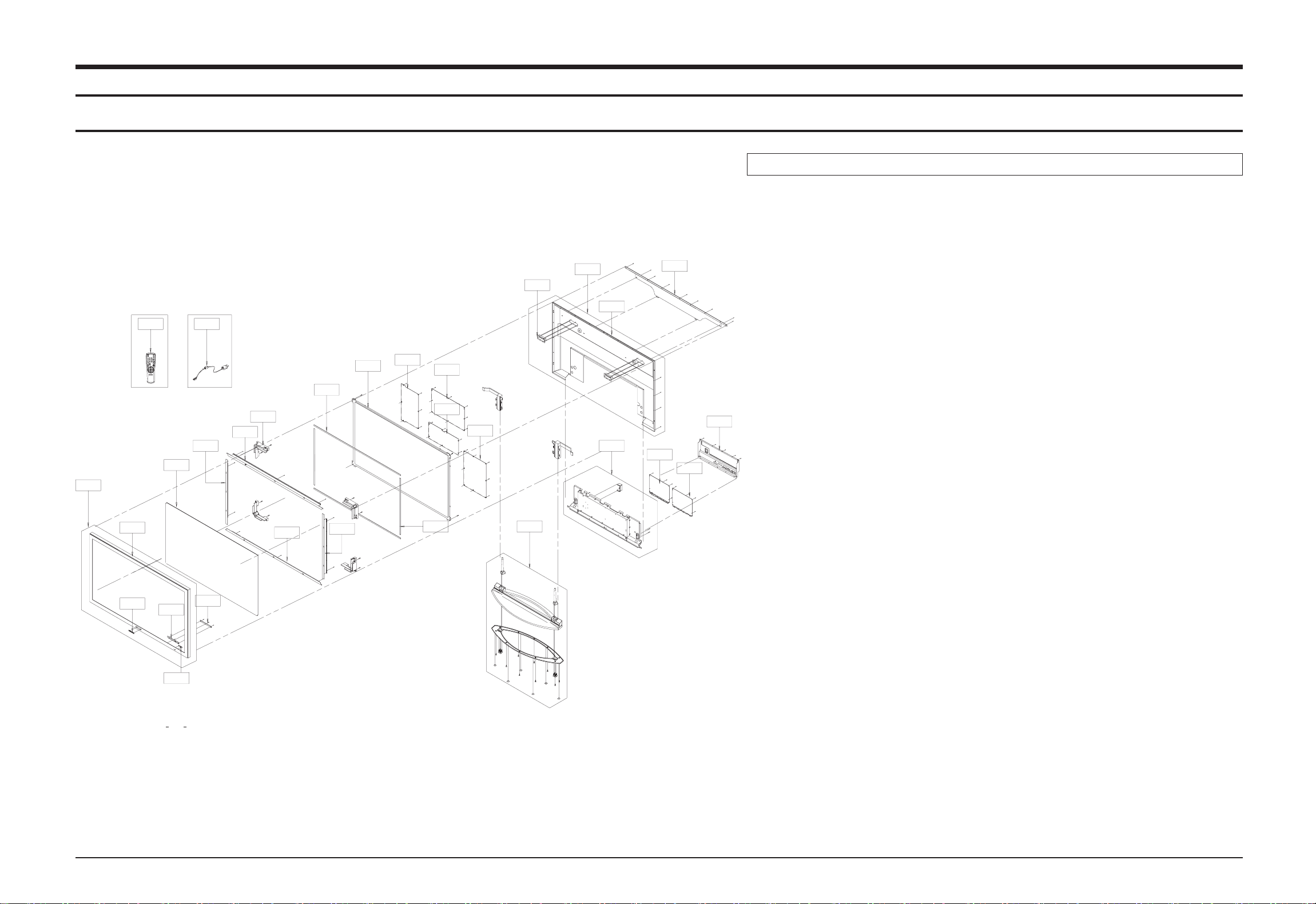
Exploded View & Parts List
Samsung Electronics 3-1
3. Exploded View & Parts List
3-1 PS42D4SX/RAD
You can search for the updated part code through ITSELF web site.
URL : http://itself.sec.samsung.co.kr
No Code No Description Specification Q’ty S.N.A
M0003 BN96-01207F ASSY COVER P-FRONT;42D4,XSA,HIPS V0,BLK 1
T0003 BN64-00280F CABINET FRONT;42D4,HIPS,V0,BKM1326+SV012 1 S.N.A
T0057 BP64-00177A BADGE-BRAND;ALL,AL,T1.5,70,11.3,BLK,SILI 1 S.N.A
T0022 BN64-00281A KNOB CONTROL;42D4,ABS,HB,BLK 1 S.N.A
T0061 BN64-00282A WINDOW-REMOCON;,PMMA CLEAR 1 S.N.A
T0098 BN94-00607A ASSY PCB MISC-CONTROL;PS42D4/42V4,D65C,N 1 S.N.A
T0456 BN67-00105A GLASS-FILTER EMI;42P3,MESH,48%,984*584,T 1
T0911 BN61-00244E BRACKET-FILTER TOP ASSY;42P3H,AL5052,1.2 1 S.N.A
T0912 BN61-00245H BRACKET-FILTER SIDE L;42P3S,AL5052,1.2 1 S.N.A
T0913 BN61-00309E BRACKET-FILTER SIDE R;42P3S,AL5052,1.2 1 S.N.A
T0914 BN61-00246E BRACKET-FILTER BOTTOM ASSY;42P3S,AL5052, 1 S.N.A
T0915 BN61-00141A HOLDER-MODULE;42P3,AL,DIECASTING 4 S.N.A
T0918 AA60-00110J SPACER-FILTER;50P3,P/U Form,20.0,2.0,5.0 2 S.N.A
T0044 BN96-01209A ASSY PDP P-MODULE;M3,S42SD-YD,V3,42INCH, 1
T0144 BN96-01208A ASSY COVER P-STAND BASE;42D4,AL5052,T1.2 1
T0764 BN96-01217A ASSY MISC P-SMPS;SPP4231,PS42D4S,110~240 1
T0073 BN96-00870A ASSY PDP P-X MAIN BOARD;M3,S42SD-YD,D65A 1
T0096 BN96-01211A ASSY PDP P-Y MAIN BOARD;M3,S42SD-YD,V3,4 1
T0037 BN96-01212A ASSY PDP P-L MAIN BOARD;M3,S42SD-YD,V3,4 1
T0008 BN96-00313D ASSY COVER P-BACK SUB;42D4,AL5052,T1.2 1 S.N.A
T0132 ASSY PCB MISC-DIGITAL;PS42D4ST,D65C,NON 1
T0145 ASSY PCB MISC-ANALOG;PS42D4ST,D65C,NELSO 1
T0001 BN96-00314B ASSY COVER P-BACK;PS42P3S,AL5052 T1.2,DG 1
T0112 BN63-00529A COVER-BACK;42P3H,AL 3031,T1.2,DGM-5810 1 S.N.A
T0916 BN61-00202A BRACKET-HANDLE;42P3S,AL5052,T1.5,DGM-S81 2 S.N.A
T0555 BN96-01280E ASSY MISC P-BRKT TERMINAL;42D4,ASIA,M/EA 1 S.N.A
T0256 BN64-00143B DECORATION-BACK;SPD-42P3H,PC+ABS,5V 1 S.N.A
T0074 AA59-00328A REMOCON;,TM75,MUSE,36,G6148,EX,EUROP 1
T0268 3903-000177 CBF-POWER CORD;DT,AU,IP3/YES,U(IEC C13-R 1
T0066T0074
T0918
T0915
T0911
T0912
T0054
P0003
T0044
T0073
T0764
T0037
T0096
T0916
T0001
T0112
T0008
T0145
T0256
T0132
T0555
T0003
T0057
T0022
T0603
T0098
T0914
T0913
T0918
T0144
Page 24
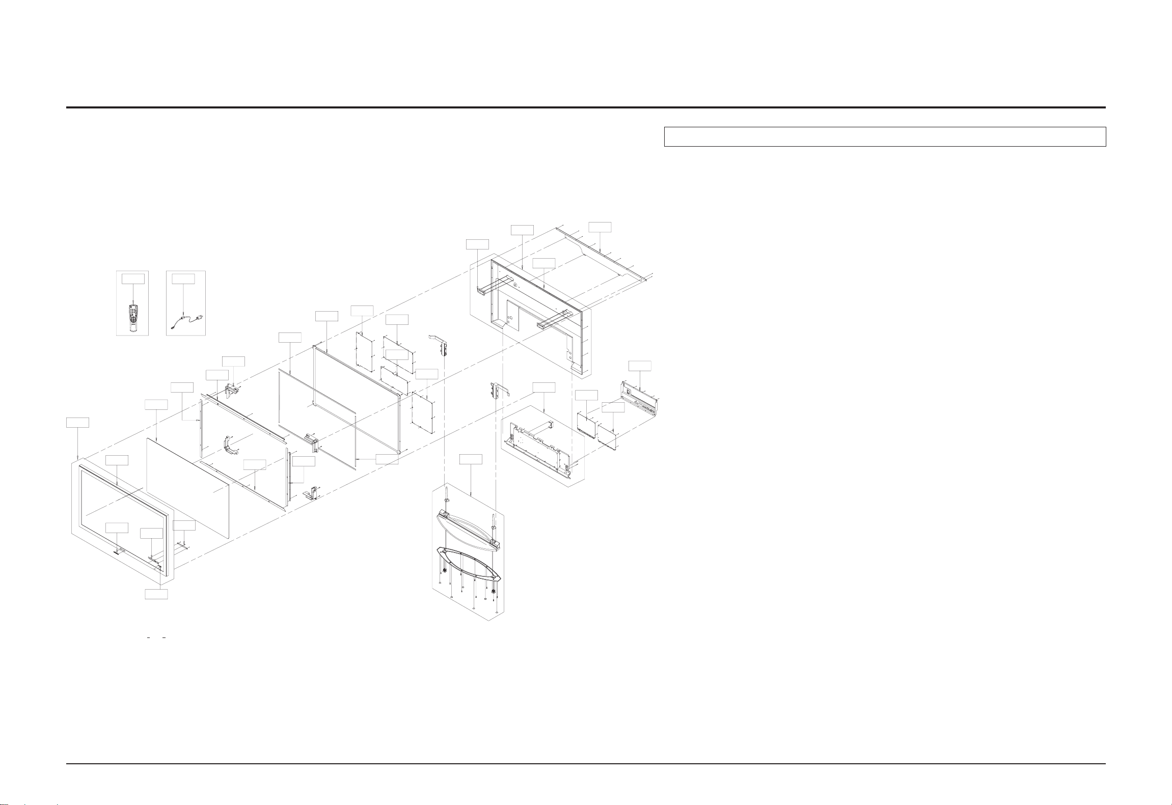
Exploded View & Parts List
3-2 Samsung Electronics
3-2 PS42D4SX/XTT
You can search for the updated part code through ITSELF web site.
URL : http://itself.sec.samsung.co.kr
No Code No Description Specification Q’ty S.N.A
M0003 BN96-01207C ASSY COVER P-FRONT;42D4,XTT,HIPS HB,BLK 1
T0003 BN64-00280C CABINET FRONT;42D4,HIPS,HB,BKM1326+SV012 1 S.N.A
T0057 BP64-00177A BADGE-BRAND;ALL,AL,T1.5,70,11.3,BLK,SILI 1 S.N.A
T0022 BN64-00281A KNOB CONTROL;42D4,ABS,HB,BLK 1 S.N.A
T0061 BN64-00282A WINDOW-REMOCON;,PMMA CLEAR 1 S.N.A
T0098 BN94-00607A ASSY PCB MISC-CONTROL;PS42D4/42V4,D65C,N 1 S.N.A
T0456 BN67-00105A GLASS-FILTER EMI;42P3,MESH,48%,984*584,T 1
T0911 BN61-00244E BRACKET-FILTER TOP ASSY;42P3H,AL5052,1.2 1 S.N.A
T0912 BN61-00245H BRACKET-FILTER SIDE L;42P3S,AL5052,1.2 1 S.N.A
T0913 BN61-00309E BRACKET-FILTER SIDE R;42P3S,AL5052,1.2 1 S.N.A
T0914 BN61-00246E BRACKET-FILTER BOTTOM ASSY;42P3S,AL5052, 1 S.N.A
T0915 BN61-00141A HOLDER-MODULE;42P3,AL,DIECASTING 4 S.N.A
T0918 AA60-00110J SPACER-FILTER;50P3,P/U Form,20.0,2.0,5.0 2 S.N.A
T0044 BN96-01209A ASSY PDP P-MODULE;M3,S42SD-YD,V3,42INCH, 1
T0144 BN96-01208A ASSY COVER P-STAND BASE;42D4,AL5052,T1.2 1
T0764 BN96-01217A ASSY MISC P-SMPS;SPP4231,PS42D4S,110~240 1
T0073 BN96-00870A ASSY PDP P-X MAIN BOARD;M3,S42SD-YD,D65A 1
T0096 BN96-01211A ASSY PDP P-Y MAIN BOARD;M3,S42SD-YD,V3,4 1
T0037 BN96-01212A ASSY PDP P-L MAIN BOARD;M3,S42SD-YD,V3,4 1
T0008 BN96-00313D ASSY COVER P-BACK SUB;42D4,AL5052,T1.2 1 S.N.A
T0132 ASSY PCB MISC-DIGITAL;PS42D4ST,D65C,NON 1
T0145 ASSY PCB MISC-ANALOG;PS42D4ST,D65C,NELSO 1
T0001 BN96-00314B ASSY COVER P-BACK;PS42P3S,AL5052 T1.2,DG 1
T0112 BN63-00529A COVER-BACK;42P3H,AL 3031,T1.2,DGM-5810 1 S.N.A
T0916 BN61-00202A BRACKET-HANDLE;42P3S,AL5052,T1.5,DGM-S81 2 S.N.A
T0555 BN96-01280D ASSY MISC P-BRKT TERMINAL;42D4,XTT,SHIEL 1 S.N.A
T0256 BN64-00143B DECORATION-BACK;SPD-42P3H,PC+ABS,5V 1 S.N.A
T0074 AA59-00312F REMOCON;Deep Impact,TM75,31,PAL,EX,PAL,M 1 S.N.A
T0268 3903-000172 CBF-POWER CORD;DT,CN,IP3/YES,U(IEC C13-R 1
T0066T0074
T0918
T0915
T0911
T0912
T0054
P0003
T0044
T0073
T0764
T0037
T0096
T0916
T0001
T0112
T0008
T0145
T0256
T0132
T0555
T0003
T0057
T0022
T0603
T0098
T0914
T0913
T0918
T0144
Page 25
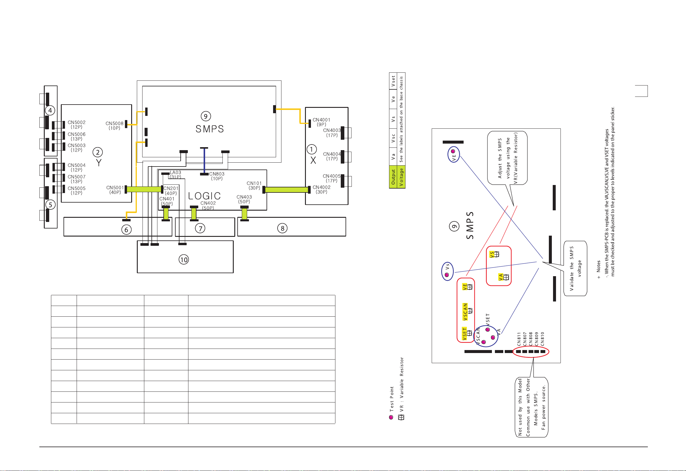
Exploded View & Parts List
Samsung Electronics 3-3
No
3-3 MODULE BLOCK
No
-
①
②
③
④
⑤
⑥
⑦
⑧
⑨
⑩
Description
ASSY PDP PANEL
ASSY PCB X MAIN
ASSY PCB Y MAIN
ASSY PCB LOGIC MAIN
ASSY PCB BUFFER(up)
ASSY PCB BUFFER(down)
ASSY PCB BUFFER(E)
ASSY PCB BUFFER(F)
ASSY PCB BUFFER(G)
ASSY PCB SMPS
ASSY PCB DIGITAL
Code No
BN96-01209A
BN96-00870A
BN96-01211A
BN96-01212A
BN96-00872A
BN96-00873A
BN96-01213A
BN96-01214A
BN96-01215A
BN96-01217A
BN94-00520A
Specification
M3,S42D-YD,V3,42INCH,SEMCO SMPS,D65A,V3.1
M3,S42SD-YD,D65A,X MAIN BOARD,LJ92-00758A,V3
M3,S42SD-YD,V3,42INCH,V3.1,SDI CODE,LJ92-00944B
M3,S42SD-YD,V3,42INCH,V3.1,SDI CODE,LJ92-00975C
M3,S42SD-YD,D65A, Y BUFFER(UP) LJ92-00796A,V3
M3,S42SD-YD,D65A, Y BUFFER LJ92-00797A,V3
M3,S42SD-YD,V3,42INCH,V3.1,SDI CODE,LJ92-00811A
M3,S42SD-YD,V3,42INCH,V3.1,SDI CODE,LJ92-00812A
M3,S42SD-YD,V3,42INCH,V3.1,SDI CODE,LJ92-00813A
SPP4231,PS42D4S,110~240V
PS42D4S,NELSON
Page 26
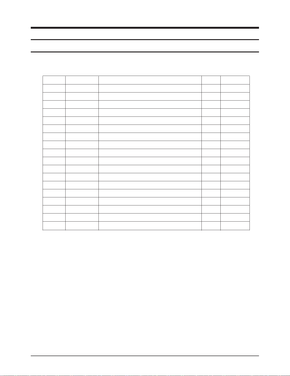
Electrical Parts List
Samsung Electronics 4-1
4. SERVICE ITEM
You can search for the updated part code through ITSELF web site.
URL : http://itself.sec.samsung.co.kr
D0254 AA32-00013B MODULE REMOCON;346HF5,38KHz,940mm,MESH,H 1
T0568 AA39-30007A CBF IF;-,T,100mm,1365#26 1
T0074 AA59-00312F REMOCON;Deep Impact,TM75,31,PAL,EX,PAL,M 1 S.N.A
TU1401 BN40-00044A TUNER;TMQZ6-407A,PAL-CS,PAL Hyper,38.9MH 1
T0079 BN94-00557A ASSY PCB MISC-MAIN;PS42D4S,D65C,CHINA 1
T0001 BN96-00314B ASSY COVER P-BACK;PS42P3S,AL5052 T1.2,DG 1
T0073 BN96-00870A ASSY PDP P-X MAIN BOARD;M3,S42SD-YD,D65A 1
T0091 BN96-00872A ASSY PDP P-Y BUFFER (UP);M3,S42SD-YD,D65 1
T0092 BN96-00873A ASSY PDP P-Y BUFFER (DOWN);M3,S42SD-YD,D 1
M0003 BN96-01207C ASSY COVER P-FRONT;42D4,XTT,HIPS HB,BLK 1
T0144 BN96-01208A ASSY COVER P-STAND BASE;42D4,AL5052,T1.2 1
T0044 BN96-01209A ASSY PDP P-MODULE;M3,S42SD-YD,V3,42INCH, 1
T0096 BN96-01211A ASSY PDP P-Y MAIN BOARD;M3,S42SD-YD,V3,4 1
T0172 AA69-02609A BAND-PP;W18,CLEA,1G 6.85 S.N.A
T0113 BN96-01213A ASSY PDP P-E BUFFER BOARD;M3,S42SD-YD,V3 1
T0114 BN96-01214A ASSY PDP P-F BUFFER BOARD;M3,S42SD-YD,V3 1
T0033 BN96-01215A ASSY PDP P-G BUFFER BOARD;M3,S42SD-YD,V3 1
T0764 BN96-01217A ASSY MISC P-SMPS;SPP4231,PS42D4S,110~240 1
Loc. Code No Description;Specification Q’ty S.N.A
4-1 PS42D4SX/XTT
Page 27
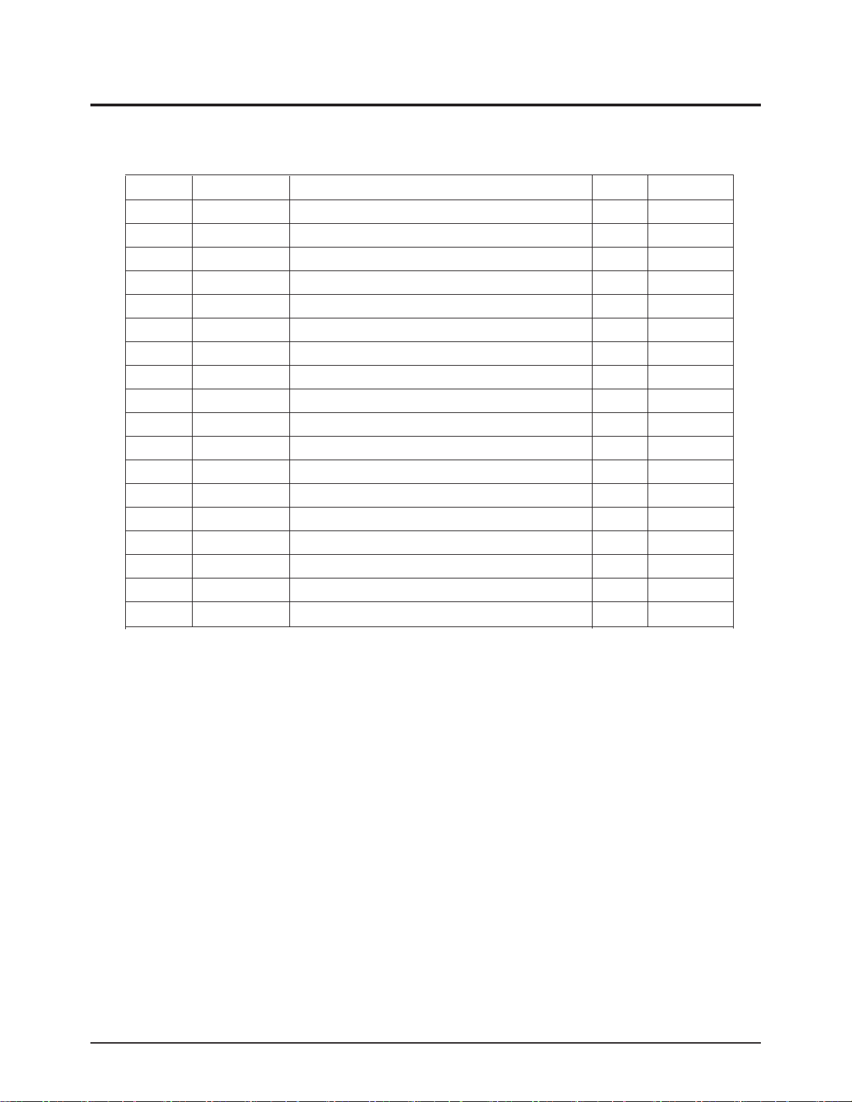
Electrical Parts List
4-2 Samsung Electronics
You can search for the updated part code through ITSELF web site.
URL : http://itself.sec.samsung.co.kr
D0254 AA32-00013B MODULE REMOCON;346HF5,38KHz,940mm,MESH,H 1
T0568 AA39-30007A CBF IF;-,T,100mm,1365#26 1
T0074 AA59-00328A REMOCON;,TM75,MUSE,36,G6148,EX,EUROP 1
TU1401 BN40-00044A TUNER;TMQZ6-407A,PAL-CS,PAL Hyper,38.9MH 1
T0079 BN94-00557A ASSY PCB MISC-MAIN;PS42D4S,D65C,CHINA 1
T0001 BN96-00314B ASSY COVER P-BACK;PS42P3S,AL5052 T1.2,DG 1
T0073 BN96-00870A ASSY PDP P-X MAIN BOARD;M3,S42SD-YD,D65A 1
T0091 BN96-00872A ASSY PDP P-Y BUFFER (UP);M3,S42SD-YD,D65 1
T0092 BN96-00873A ASSY PDP P-Y BUFFER (DOWN);M3,S42SD-YD,D 1
M0003 BN96-01207F ASSY COVER P-FRONT;42D4,XSA,HIPS V0,BLK 1
T0144 BN96-01208A ASSY COVER P-STAND BASE;42D4,AL5052,T1.2 1
T0044 BN96-01209A ASSY PDP P-MODULE;M3,S42SD-YD,V3,42INCH, 1
T0096 BN96-01211A ASSY PDP P-Y MAIN BOARD;M3,S42SD-YD,V3,4 1
T0172 AA69-02609A BAND-PP;W18,CLEA,1G 6.85 S.N.A
T0113 BN96-01213A ASSY PDP P-E BUFFER BOARD;M3,S42SD-YD,V3 1
T0114 BN96-01214A ASSY PDP P-F BUFFER BOARD;M3,S42SD-YD,V3 1
T0033 BN96-01215A ASSY PDP P-G BUFFER BOARD;M3,S42SD-YD,V3 1
T0764 BN96-01217A ASSY MISC P-SMPS;SPP4231,PS42D4S,110~240 1
Loc. Code No Description;Specification Q’ty S.N.A
4-2 PS42D4SX/RAD
Page 28
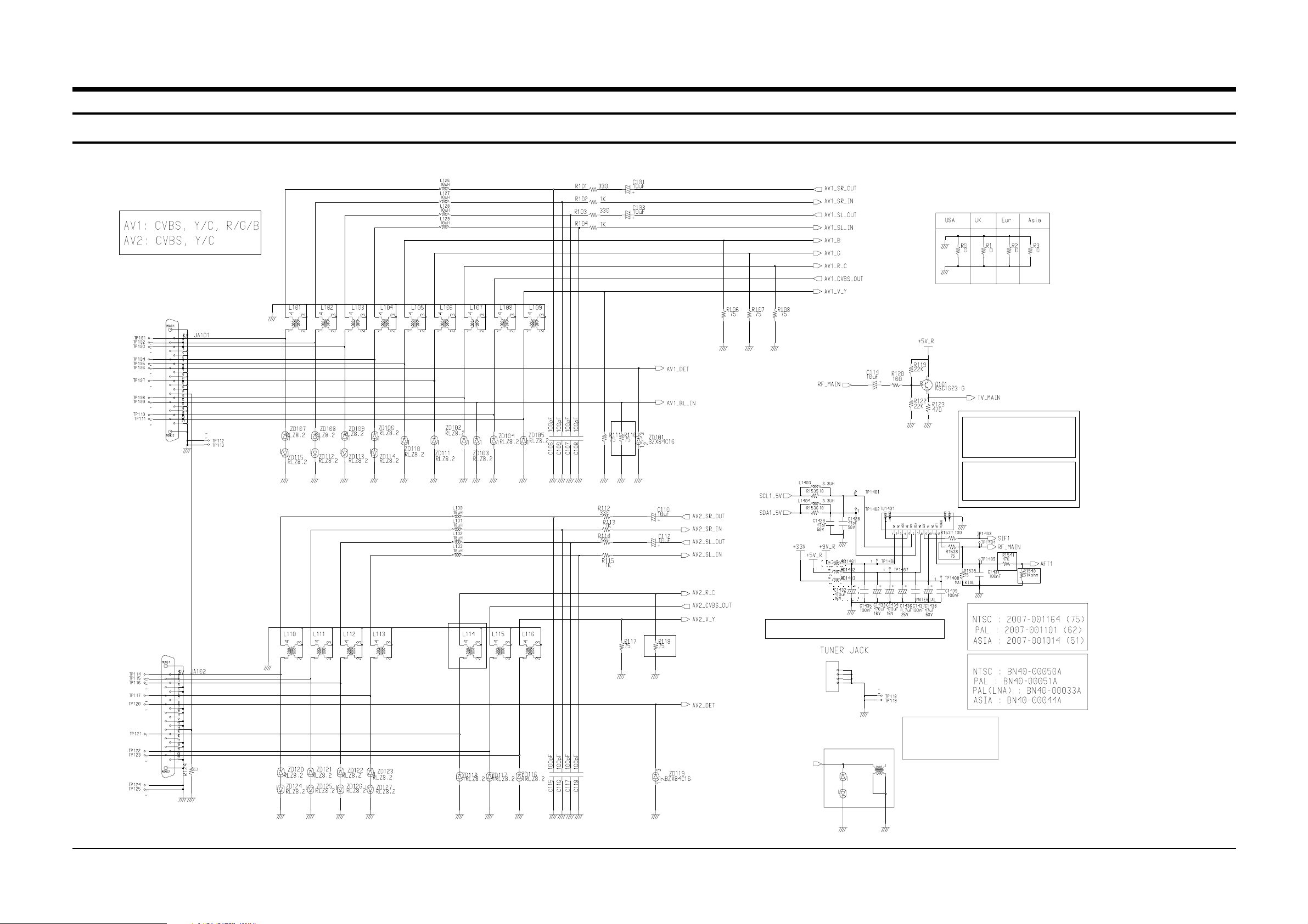
NTSC : 2007-001010 (51K)
R110 NTSC/PAL ADD OPTION
CN1402
BD1401,C1432 LNA OPTION
NTSC : 3705-001326
R118, L114 NTSC DELETE
PAL : 2007-000097 (47K)
PAL : 3705-001328
R1538
TU1401 (Tuner)
R1540
PAL : 2007-000130 (39K)
NTSC : 2007-000097 (47K)
R1541
L1405
1
23
4
INSTPAR
ZD1401
RLZ8.2
1
2
3
4
CN1402
RLZ8.2
ZD1402
WOOPER
5. Schematic Diagrams
Samsung Electronics
Schematic Diagrams
5-1
5-1 SCART
This Document can not be used without Samsung’s authorization.
Page 29
Schematic Diagrams
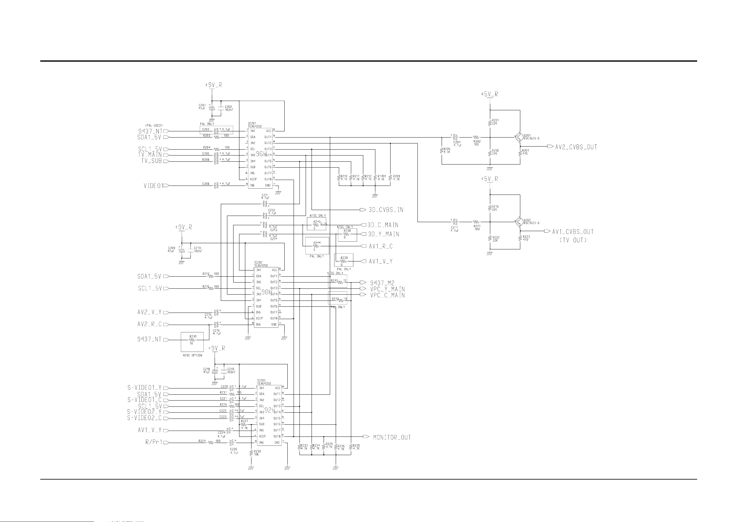
5-2 Samsung Electronics
5-2 VIDEO SW
This Document can not be used without Samsung’s authorization.
Page 30
Samsung Electronics
Schematic Diagrams
5-3
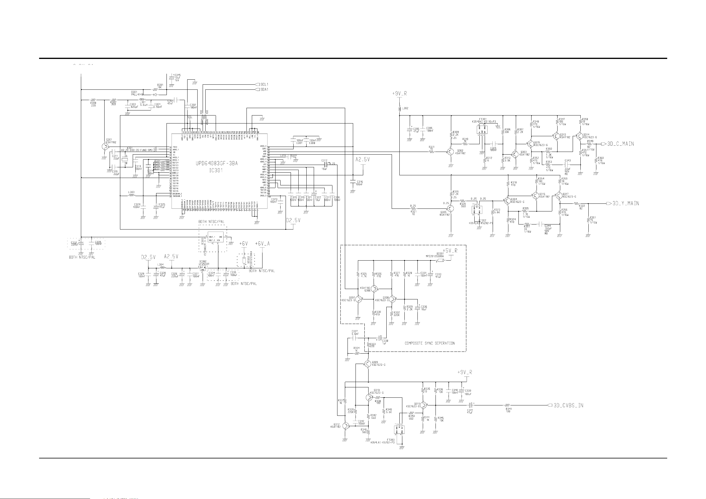
5-3 3D COMB
This Document can not be used without Samsung’s authorization.
Page 31
Schematic Diagrams
5-4 Samsung Electronics
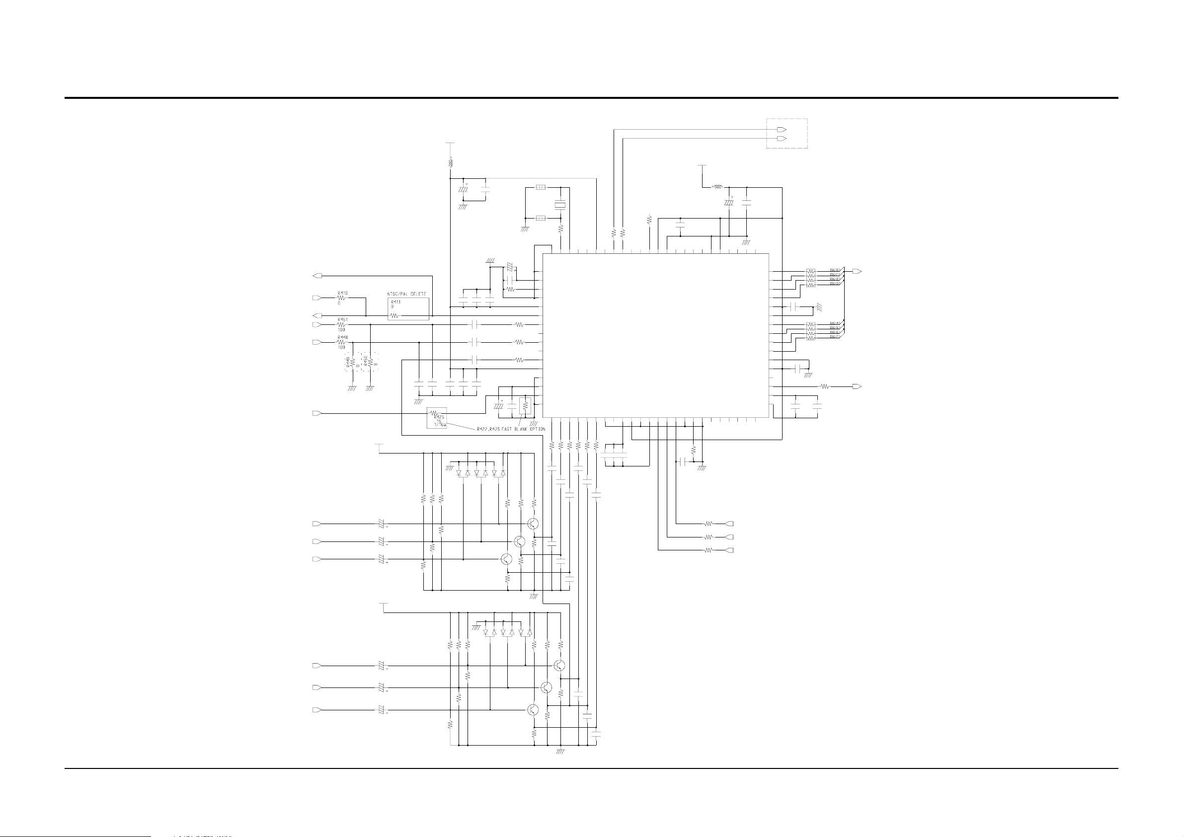
5-4 VPC3230
This Document can not be used without Samsung’s authorization.
9437_NT
9437_M2
CVBS_TTX
VPC_C_MAIN
VPC_Y_MAIN
AV1_BL_IN
AV1_B
AV1_G
AV1_R_C
+9V_R
C442
47uF
16V
C443
47uF
16V
C445
47uF
16V
+9V_R
C426
100pF
R433
15K
1/16W
R445
10K
1/16W
+5V_VPC
C429
100pF
R432
15K
1/16W
C430
220nF
SDS7000
R434
15K
1/16W
R440
10K
1/16W
R443
10K
1/16W
3.3UH
C414
220nF
C422
C424
D401
L401
C431
1.5nF
3
C401
100uF
C415
1.5nF
SDS7000
12
330nFC420
1uF
1uF
C428
0.39nF
D402
12
3
Q403
KSC1623-Y
D406
SDS7000
C402
100nF
C416
0.39nF
C434
100uF
16V
SDS7000
Q402
KSC1623-Y
C411
10uF
R415
R420 47
C427
47nF
D403
12
3
R436
B
C
B
E
R446
1K
D405
SDS7000
C413
47nF
R408
0
47
47R417
R422
1K
10
B
C
E
R444
1K
D404
SDS7000
R437
C403
5pF
C409
5pF
65
66
67
68
69
70
71
72
73
74
75
76
77
78
79
80
10
C
Q401
KSC1623-Y
E
R442
1K
HC-49/SM5H(20.25MHz)
64
ASGF_2
GNDF
VRT
I2CSEL
ISGND
VSUPF
VOUT
CIN
VIN1
VIN2
VIN3
VIN4
VSUPAI
GNDAI
VREF
FB1IN
AISGND
B1
1
47R429
220nF
C439
R435
10
C444
R427 47
C440
100pF
C446
Q0Q1
R402
33
63
XTAL2
G1
2
220nF
100pF
X401
R1
3
47R428
C441
C447
62
XTAL1
220nF
100pF
B2
4
R447 47
C448
61
NC_2
220nF
60
G2
47R407
C406
CLK5
220nF
R2
6
47R426
C407
R403
47
59
VSTBY
C436
220nF
220nF
58
FPDAT
ASGF_1
7
C435
1.5nF
NC_1
8
57
VS
R401
100
R404
47
53
56
55
54
FSY
AVO
MSY
INTLC
IC401
VPC3230D-C5
MAIN
VSUPCAP
VSUPD
GNDCAP
GNDD
9
10
12
11
C437
0.39nF
52
VSUPSY
SCL
135
51
GNDSY
SDA
14
50
C0
RESQ
15
C438
100nF
+3.3V_R
C408
1nF
49 48C247
C1
TEST
VGAV
16
17
100 R441
100 R439
100 R438
100uF
C3
YCOEQ
18
R431
1K
C405
16V
46
GNDC
FFIE
19
L402
3.3UH
45
VSUPC
FFWE
20
44
43 42
C4
C5
FFRSTW
FFRE
22
21
ASI_RESET
SDA1
SCL1
FLI2310_MAIN DEINTERLACE
VOUT
HOUT
C404
100nF
25V
MO
41
C6
C7
Y0
40
Y1
39
Y2
38
Y3
37
VSUPY
36
GNDY
35
Y4
34
Y5
33
Y6
32
Y7
31
GNDLLC
30
LLC1
LLC2
GNDPA
CLK20
24
C425
29
100nF
28
27
26
25
FFOE
23
VSUPLLC
VSUPPA
C418
100nF
C432
47nF
RA401
47
1
3
5
7
1
3
5
7
RA402
47
2
4
6
8
2
4
6
8
R423
1/16W
C433
1.5nF
656(0:7)
FLI2310_MAIN DEINTERLACE
47
656CLK
FLI2310_MAIN DEINTERLACE
12
12
3
Q405
KSC1623-Y
Q406
KSC1623-Y
12
3
R430
B
C
B
E
R419
1K
10
R406
10
R409
10
C
Q404
B
KSC1623-Y
E
C
R416
E
1K
C417
R418
1K
1.5nF
C410
C412
470pF
1.5nF
COMP1_Pb
COMP1_Y
COMP1_Pr
47uF
16V
47uF
16V
47uF
16V
C421
C423
C419
R413
15K
R414
10K
R412
15K
R405
15K
R421
10K
R424
10K
3
Page 32
Samsung Electronics
Schematic Diagrams
5-5
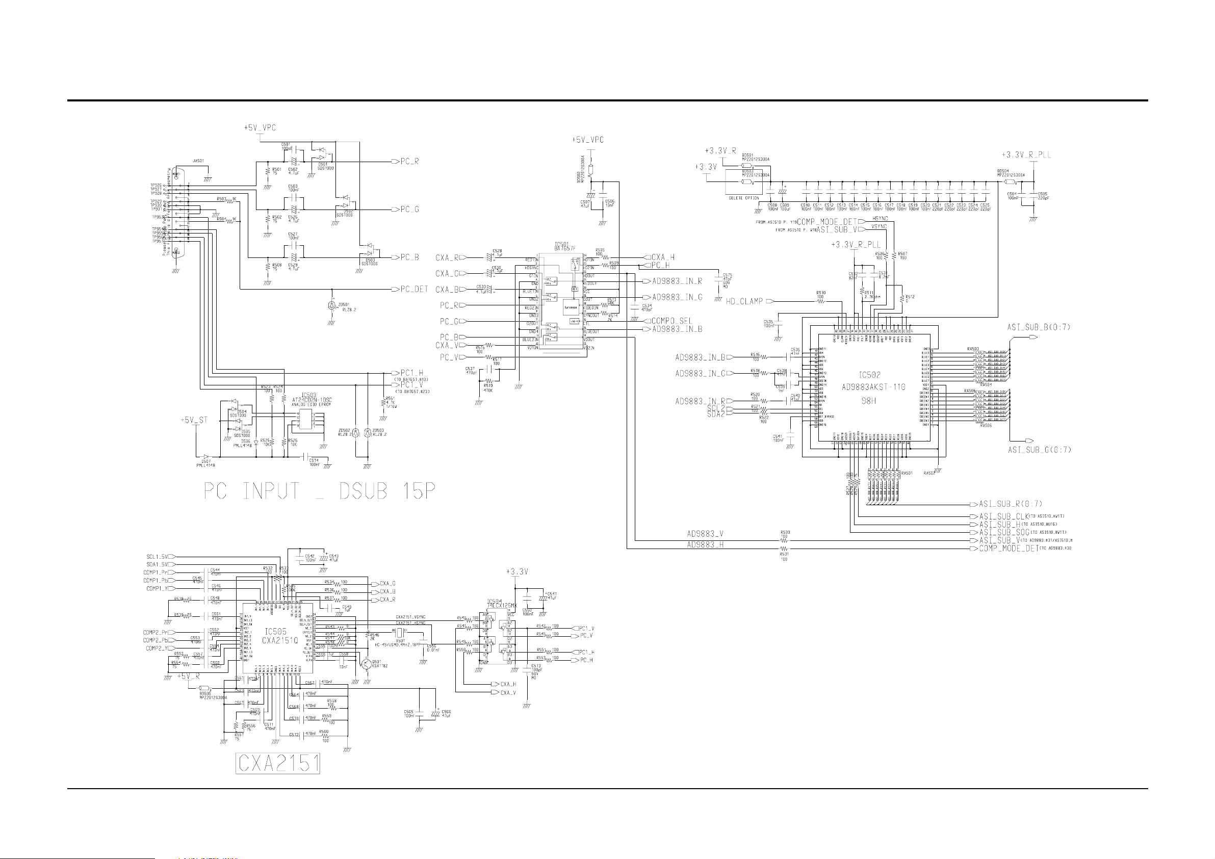
5-5 PCIN_9883_2151
This Document can not be used without Samsung’s authorization.
8EH
Page 33
Schematic Diagrams
5-6 Samsung Electronics
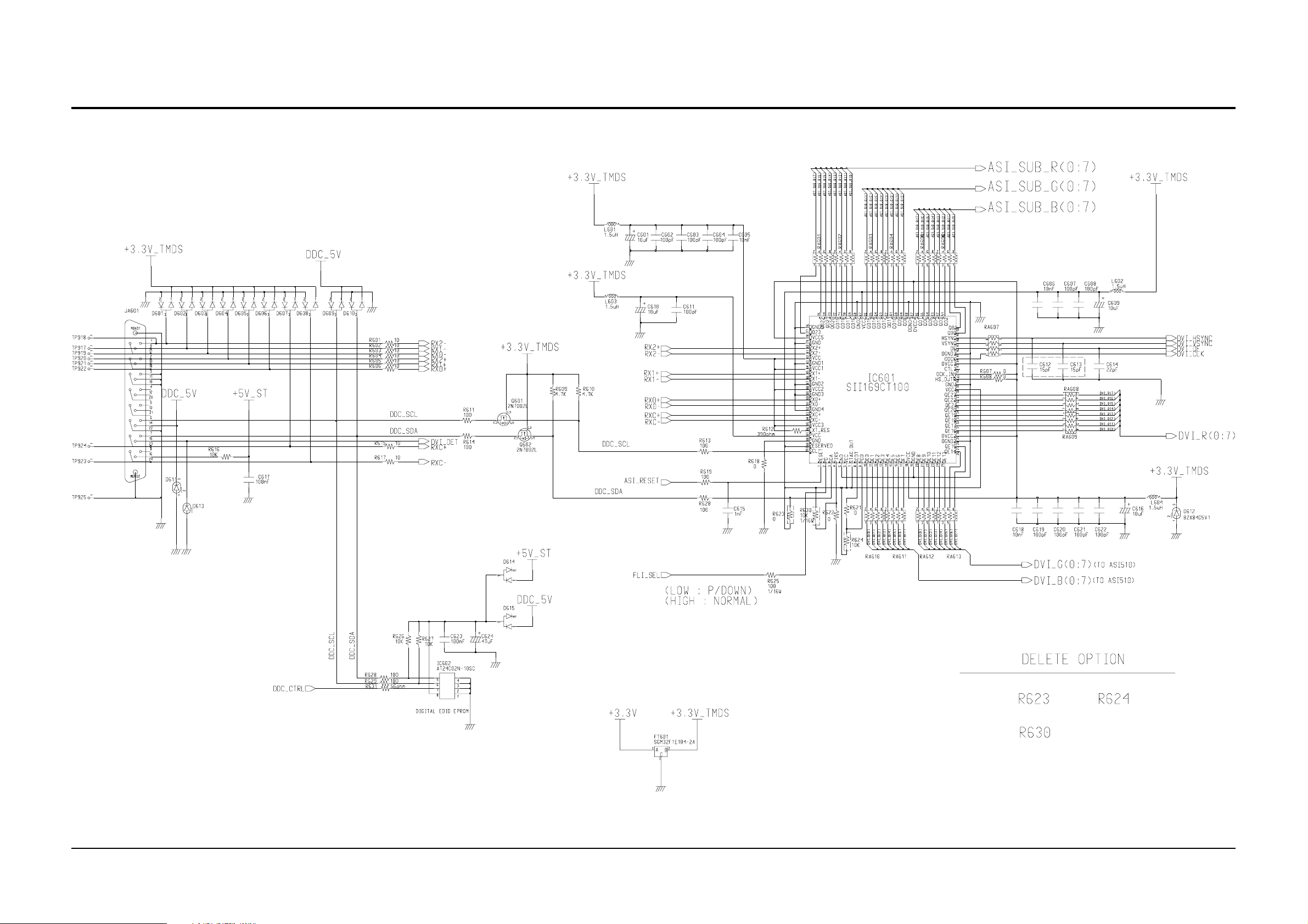
5-6 DVI_SIL169
This Document can not be used without Samsung’s authorization.
Page 34
Samsung Electronics
Schematic Diagrams
5-7
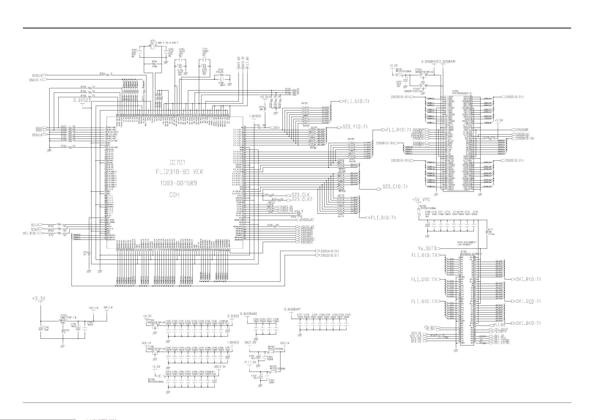
5-7 FLI2310
This Document can not be used without Samsung’s authorization.
Page 35
Schematic Diagrams
Samsung Electronics5-8
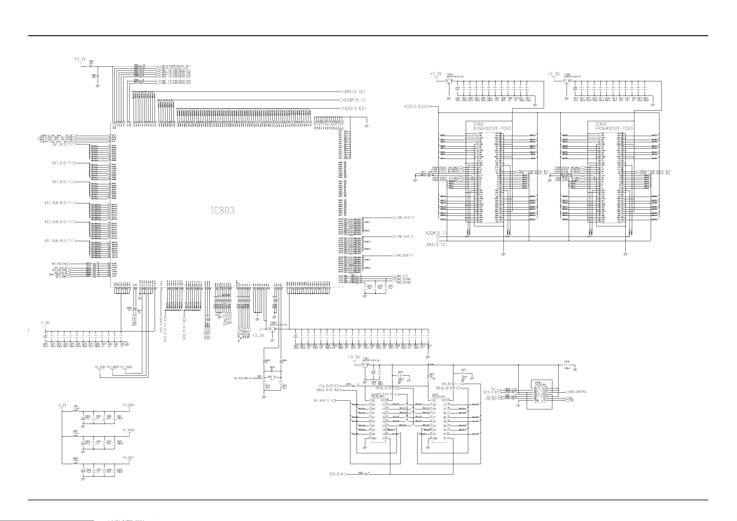
5-8 ASI510
3EH
ASI510
This Document can not be used without Samsung’s authorization.
Page 36
Samsung Electronics
Schematic Diagrams
5-9
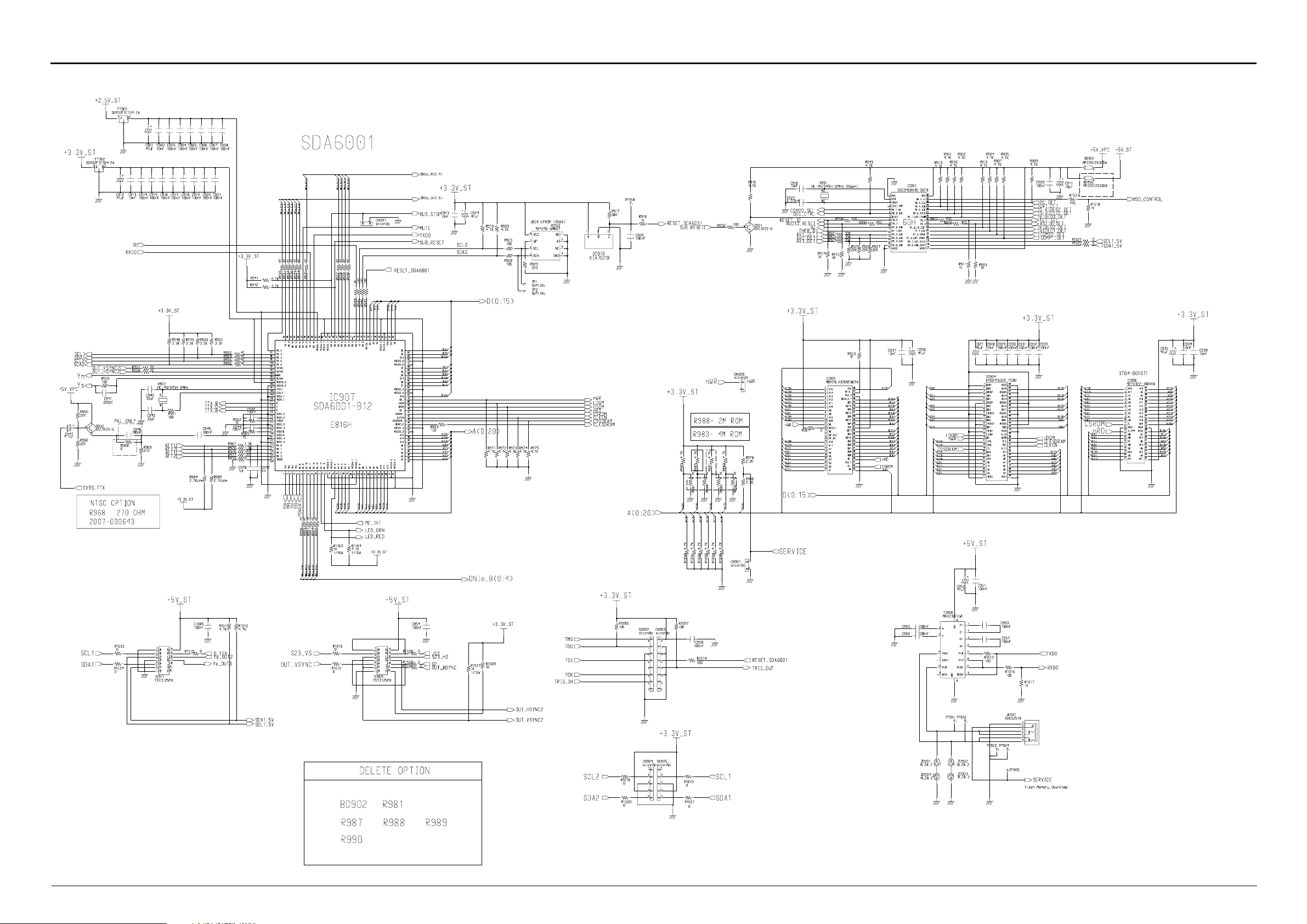
5-9 SDA6001
This Document can not be used without Samsung’s authorization.
Page 37
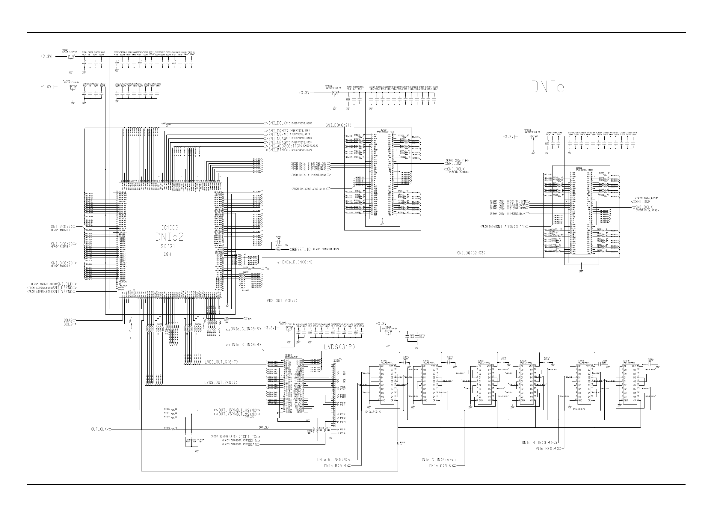
5-10 DNIe2
5-10
Schematic Diagrams
Samsung Electronics
This Document can not be used without Samsung’s authorization.
Page 38
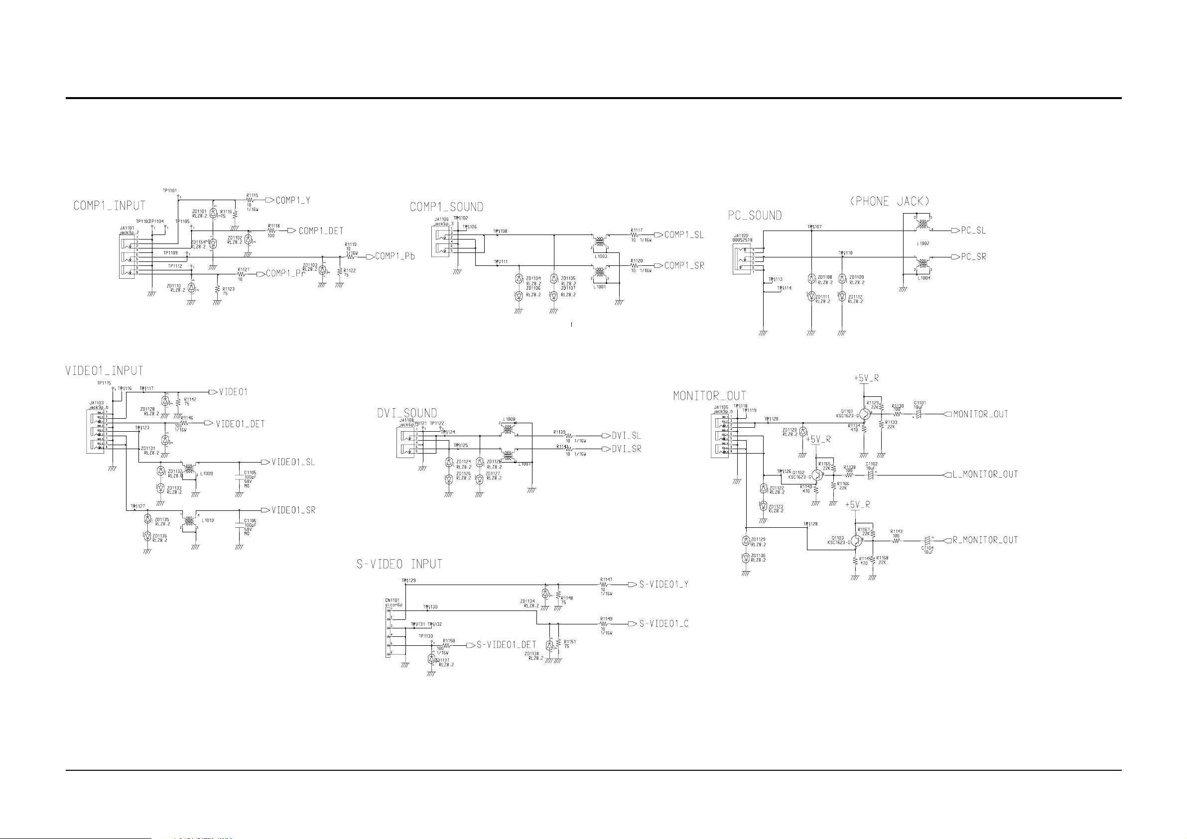
Samsung Electronics
Schematic Diagrams
5-11
5-11 JACK INPUT
This Document can not be used without Samsung’s authorization.
Page 39
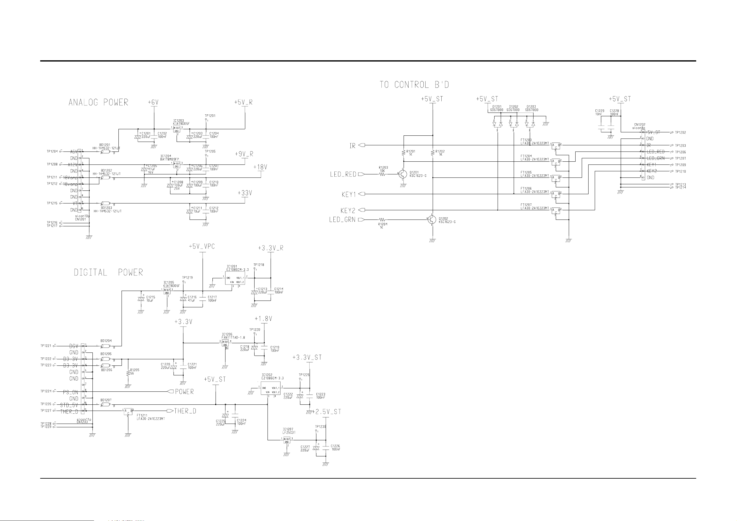
Schematic Diagrams
5-12 Samsung Electronics
5-12 POWER
This Document can not be used without Samsung’s authorization.
Page 40
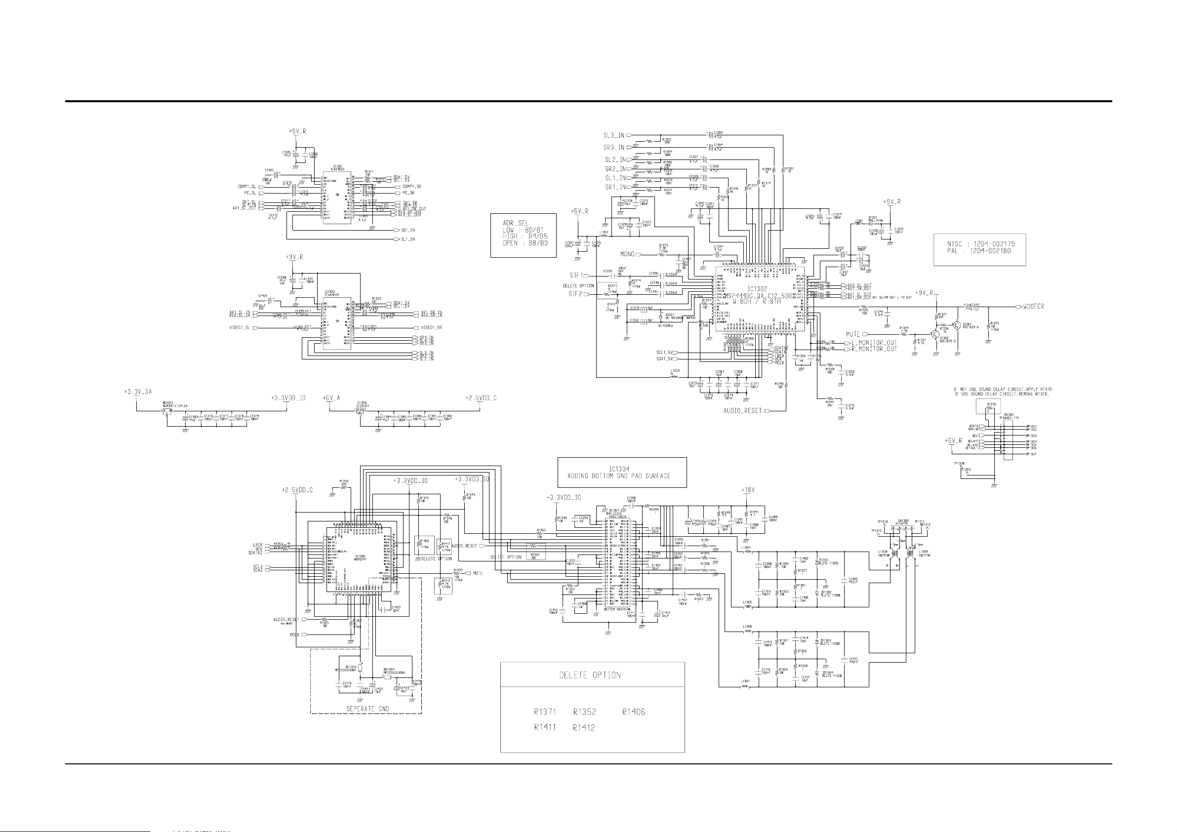
Samsung Electronics
Schematic Diagrams
5-13
5-13 AUDIO
This Document can not be used without Samsung’s authorization.
NSP6241
 Loading...