

240pin Registered DIMM
http://www.BDTIC.com/SAMSUNG
1.35V
based on 4Gb A-die
78FBGA with Lead-Free & Halogen-Free
(RoHS compliant)
Rev. 1.0, Jul. 2010
M393B2G70AH0
M393B2G73AH0
M393B4G70AM0
datasheet
SAMSUNG ELECTRONICS RESERVES THE RIGHT TO CHANGE PRODUCTS, INFORMATION AND
SPECIFICATIONS WITHOUT NOTICE.
Products and specifications discussed herein are for reference purposes only. All information discussed
herein is provided on an "AS IS" basis, without warranties of any kind.
This document and all information discussed herein remain the sole and exclusive property of Samsung
Electronics. No license of any patent, copyright, mask work, trademark or any other intellectual property
right is granted by one party to the other party under this document, by implication, estoppel or otherwise.
Samsung products are not intended for use in life support, critical care, medical, safety equipment, or
similar applications where product failure could result in loss of life or personal or physical harm, or any
military or defense application, or any governmental procurement to which special terms or provisions
may apply.
For updates or additional information about Samsung products, contact your nearest Samsung office.
All brand names, trademarks and registered trademarks belong to their respective owners.
ⓒ 2010 Samsung Electronics Co., Ltd. All rights reserved.
- 1 -

Rev. 1.0
http://www.BDTIC.com/SAMSUNG
Registered DIMM
datasheet DDR3L SDRAM
Revision History
Revision No. History Draft Date Remark Editor
1.0 - First Release Jul. 2010 - S.H.Kim
- 2 -
Rev. 1.0
http://www.BDTIC.com/SAMSUNG
Registered DIMM
datasheet DDR3L SDRAM
Table Of Contents
240pin Registered DIMM based on 4Gb A-die
1. DDR3L Registered DIMM Ordering Information ........................................................................................................... 4
2. Key Features.................................................................................................................................................................4
3. Address Configuration ..................................................................................................................................................4
4. Registered DIMM Pin Configurations (Front side/Back side)........................................................................................ 5
5. Pin Description .............................................................................................................................................................6
6. ON DIMM Thermal Sensor ...........................................................................................................................................6
7. Input/Output Functional Description..............................................................................................................................7
8. Pinout Comparison Based On Module Type................................................................................................................. 8
9. Registering Clock Driver Specification..........................................................................................................................9
9.1 Timing & Capacitance values ..................................................................................................................................9
9.2 Clock driver Characteristics.....................................................................................................................................9
10. Function Block Diagram:............................................................................................................................................. 10
10.1 16GB, 2Gx72 Module (Populated as 2 ranks of x4 DDR3 SDRAMs) ................................................................... 10
10.2 16GB, 2Gx72 Module (Populated as 4 ranks of x8 DDR3 SDRAMs) ................................................................... 12
10.3 32GB, 4Gx72 Module (Populated as 4 ranks of x4 DDR3 SDRAMs) ................................................................... 13
11. Absolute Maximum Ratings ........................................................................................................................................18
11.1 Absolute Maximum DC Ratings............................................................................................................................. 18
11.2 DRAM Component Operating Temperature Range .............................................................................................. 18
12. AC & DC Operating Conditions...................................................................................................................................18
12.1 Recommended DC Operating Conditions (SSTL-15)............................................................................................18
13. AC & DC Input Measurement Levels ..........................................................................................................................19
13.1 AC & DC Logic Input Levels for Single-ended Signals.......................................................................................... 19
13.2 V
13.3 AC and DC Logic Input Levels for Differential Signals .......................................................................................... 22
13.3.1. Differential Signals Definition ......................................................................................................................... 22
13.3.2. Differential Swing Requirement for Clock (CK - CK
13.3.3. Single-ended Requirements for Differential Signals ...................................................................................... 24
13.3.4. Differential Input Cross Point Voltage ............................................................................................................ 25
13.4 Slew Rate Definition for Single Ended Input Signals .............................................................................................26
13.5 Slew rate definition for Differential Input Signals ................................................................................................... 26
14. AC & DC Output Measurement Levels .......................................................................................................................26
14.1 Single Ended AC and DC Output Levels............................................................................................................... 26
14.2 Differential AC and DC Output Levels ................................................................................................................... 26
14.3 Single-ended Output Slew Rate ............................................................................................................................ 27
14.4 Differential Output Slew Rate ................................................................................................................................ 28
15. IDD specification definition..........................................................................................................................................29
16. IDD SPEC Table .........................................................................................................................................................31
17. Input/Output Capacitance ........................................................................................................................................... 33
18. Electrical Characteristics and AC timing .....................................................................................................................34
18.1 Refresh Parameters by Device Density.................................................................................................................34
18.2 Speed Bins and CL, tRCD, tRP, tRC and tRAS for Corresponding Bin ................................................................ 34
18.3 Speed Bins and CL, tRCD, tRP, tRC and tRAS for corresponding Bin ................................................................. 34
18.3.1. Speed Bin Table Notes ..................................................................................................................................36
19. Timing Parameters by Speed Grade ..........................................................................................................................38
19.1 Jitter Notes ............................................................................................................................................................ 41
19.2 Timing Parameter Notes........................................................................................................................................ 42
20. Physical Dimensions...................................................................................................................................................43
20.1 1Gbx4 based 2Gx72 Module (2 Ranks) - M393B2G70AH0..................................................................................43
20.1.1. x72 DIMM, populated as two physical ranks of x4 DDR3 SDRAMs .............................................................. 43
20.2 512Mbx8 based 2Gx72 Module (4 Ranks) - M393B2G73AH0.............................................................................. 44
20.2.1. x72 DIMM, populated as four physical ranks of x8 DDR3 SDRAMs .............................................................. 44
20.3 2Gbx4(DDP) based 4Gx72 Module (4 Ranks) - M393B4G70AM0 ....................................................................... 45
20.3.1. x72 DIMM, populated as four physical ranks of x4 DDR3 SDRAMs .............................................................. 45
20.3.2. Heat Spreader Design Guide ......................................................................................................................... 46
Tolerances.................................................................................................................................................... 21
REF
) and Strobe (DQS - DQS) ............................................. 22
- 3 -
Rev. 1.0
http://www.BDTIC.com/SAMSUNG
Registered DIMM
datasheet DDR3L SDRAM
1. DDR3L Registered DIMM Ordering Information
Part Number
M393B2G70AH0-YF7/F8/H9 16GB 2Gx72 1Gx4(K4B4G0446A-HY##)*36 2 30mm
M393B2G73AH0-YF7/F8/H9 16GB 2Gx72 512Mx8(K4B4G0846A-HY##)*36 4 30mm
M393B4G70AM0-YF7/F8/H9 32GB 4Gx72 DDP 2Gx4(K4B8G0446A-MY##)*36 4 30mm
NOTE :
1. "##" - F7/F8/H9
2. F7(800Mbps 6-6-6) / F8(1066Mbps 7-7-7) / H9(1333Mbps 9-9-9)
- DDR3-1333(9-9-9) is backward compatible to DDR3-1066(7-7-7) DDR3-800(6-6-6)
- DDR3-1066(7-7-7) is backward compatible to DDR3-800(6-6-6)
2
Density Organization Component Composition
Number of
Rank
Height
2. Key Features
Speed
tCK(min) 2.5 1.875 1.5 ns
CAS Latency 6 7 9nCK
tRCD(min) 15 13.125 13.5 ns
tRP(min) 15 13.125 13.5 ns
tRAS(min) 37.5 37.5 36 ns
tRC(min) 52.5 50.625 49.5 ns
DDR3-800 DDR3-1066 DDR3-1333
6-6-6 7-7-7 9-9-9
Unit
• JEDEC standard 1.35V(1.28V~1.45V) & 1.5V(1.425V~1.575V) Power Supply
= 1.35V(1.28V~1.45V) & 1.5V(1.425V~1.575V)
•V
DDQ
• 400MHz f
• 8 independent internal bank
• Programmable
• Programmable Additive Latency(Posted
• Programmable
• Burst Length: 8 (Interleave without any limit, sequential with st
write [either On the fly using A12 or MRS]
• Bi-directional Differential Data Strobe
• On Die Termination using ODT pin
• Average Refresh Period 7.8us at lower then T
• Asynchronous Reset
for 800Mb/sec/pin, 533MHz fCK for 1066Mb/sec/pin, 667MHz fCK for 1333Mb/sec/pin
CK
CAS Latency: 6,7,8,9
CAS Write Latency(CWL) = 5(DDR3-800), 6(DDR3-1066) and 7(DDR3-1333)
CAS) : 0, CL - 2, or CL - 1 clock
arting address “000” only), 4 with tCCD = 4 which does not allow seamless read or
85°C, 3.9us at 85°C < T
CASE
CASE
≤ 95°C
3. Address Configuration
Organization Row Address Column Address Bank Address Auto Precharge
1Gx4(4Gb) based Module A0-A15 A0-A9, A11 BA0-BA2 A10/AP
512Mx8(4Gb) based Module A0-A15 A0-A9 BA0-BA2 A10/AP
2Gx4(8Gb DDP) based Module A0-A15 A0-A9, A11 BA0-BA2 A10/AP
- 4 -

Rev. 1.0
http://www.BDTIC.com/SAMSUNG
Registered DIMM
datasheet DDR3L SDRAM
4. Registered DIMM Pin Configurations (Front side/Back side)
Pin Front Pin Back Pin Front Pin Back Pin Front Pin Back
1
2
V
REFDQ
V
121
SS
122 DQ4 43 DQS8 163
3DQ0123DQ544
4DQ1124
5
6DQS
V
SS
125
0126
7DQS0127
8
V
SS
128 DQ6 KEY 89
9DQ2129DQ749
10 DQ3 130
11
V
SS
131 DQ12 51
12 DQ8 132 DQ13 52 BA2 172 A14 93 DQS
13 DQ9 133
14
15 DQS
V
SS
134
1135
16 DQS1 136
17
V
SS
137 DQ14 57
18 DQ10 138 DQ15 58 A5 178 A6 99 DQ48 219 DQ53
19 DQ11 139
20
V
SS
140 DQ20 60
21 DQ16 141 DQ21 61 A2 181 A1 102 DQS
22 DQ17 142
23
24 DQS
V
SS
143
2144
25 DQS2 145
26
V
SS
146 DQ22 66
27 DQ18 147 DQ23 67
28 DQ19 148
29
V
SS
149 DQ28 69
30 DQ24 150 DQ29 70 A10/AP 190 BA1 111 DQS
31 DQ25 151
32
33 DQS
V
SS
152
3153
34 DQS3 154
35
V
SS
155 DQ30 75
36 DQ26 156 DQ31 76 S1,NC 196 A13 117 SA0 237 SA1
37 DQ27 157
38
V
SS
158 CB4,NC 78
39 CB0,NC 159 CB5,NC 79 S2,NC 199
40 CB1,NC 160
41
V
SS
161
NOTE : NC = No internal Connection
V
SS
V
SS
DM0,DQS9
,TDQS9
NC,DQS
9
9
,TDQS
V
SS
V
SS
V
SS
DM1,DQS10
,TDQS10
NC,DQS
10
10
,TDQS
V
SS
V
SS
V
SS
DM2,DQS11
,TDQS11
NC,DQS
11
,TDQS
11
V
SS
V
SS
V
SS
DM3,DQS12
,TDQS12
NC,DQS
12
12
,TDQS
V
SS
V
SS
V
SS
DM8,DQS17
TDQS17,NC
42 DQS8162
V
SS
164 CB6,NC 84 DQS4 204
45 CB2,NC 165 CB7,NC 85 DQS4 205
46 CB3,NC 166
47
48
V
SS
, NC
V
TT
V
, NC
TT
167 NC(TEST) 87 DQ34 207 DQ39
168 RESET
169 CKE1, NC 90 DQ40 210 DQ45
50 CKE0 170
V
DD
171 A15 92
53 Err_Out/NC 173
54
V
DD
174 A12/BC 95
55 A11 175 A9 96 DQ42 216 DQ47
56 A7 176
V
DD
177 A8 98
59 A4 179
V
DD
62
V
DD
180 A3 101
182
63 NC, CK1 183
64 NC, CK
65
1 184 CK0 105 DQ50 225 DQ55
V
REFCA
V
DD
V
DD
185 CK0 106 DQ51 226
186
187 EVENT,NC 108 DQ56 228 DQ61
68 NC/Par_In 188 A0 109 DQ57 229
V
DD
189
71 BA0 191
72
73 WE
V
DD
192 RAS 113
193 S0 114 DQ58 234 DQ63
74 CAS 194
V
DD
195 ODT0 116
77 ODT1,NC 197
V
DD
80
V
SS
198 S3,NC 119 SA2 239
200 DQ36
81 DQ32 201 DQ37
SAMSUNG ELECTRONICS CO., Ltd. reserves the right to change products and specifications without notice.
NC,DQS
,TDQS
V
SS
V
SS
V
DD
V
DD
V
DD
V
DD
V
DD
V
DD
V
DD
V
DD
V
DD
V
DD
V
DD
V
SS
17
17
82 DQ33 202
83
86
V
SS
V
SS
203
206 DQ38
DM4,DQS13
88 DQ35 208
V
SS
209 DQ44
91 DQ41 211
V
SS
212
DM5,DQS14
5 213
94 DQS5 214
V
SS
215 DQ46
97 DQ43 217
V
SS
218 DQ52
100 DQ49 220
V
SS
221
DM6,DQS15
6 222
103 DQS6 223
104
107
110
V
SS
V
SS
V
SS
7 231
224 DQ54
227 DQ60
230
DM7/DQS16
DM7,DQS
112 DQS7 232
V
SS
233 DQ62
115 DQ59 235
V
SS
236
118 SCL 238 SDA
120
V
TT
240
V
SS
,TDQS13
NC,DQS
,TDQS
V
SS
V
SS
V
SS
,TDQS14
NC,DQS
,TDQS
V
SS
V
SS
V
SS
,TDQS15
NC,DQS
,TDQS
V
SS
V
SS
V
SS
TDQS16
,TDQS
V
SS
V
SS
V
DDSPD
V
SS
V
TT
13
13
14
14
15
15
16
16
- 5 -
Rev. 1.0
http://www.BDTIC.com/SAMSUNG
Registered DIMM
datasheet DDR3L SDRAM
5. Pin Description
Pin Name Description Number Pin Name Description Number
CK0 Clock Input, positive line 1 ODT[1:0] On Die Termination Inputs 2
CK0
CKE[1:0] Clock Enables 2 CB[7:0] Data check bits Input/Output 8
RAS
CAS
WE
[3:0] Chip Selects 4
S
A[9:0],A11,
A[15:13]
A10/AP Address Input/Autoprecharge 1 EVENT
A12/BC
BA[2:0] SDRAM Bank Addresses 3 RESET
SCL Serial Presence Detect (SPD) Clock Input 1
SDA SPD Data Input/Output 1
SA[2:0] SPD Address Inputs 3
Par_In Parity bit for the Address and Control bus 1
Err_Out
NOTE :
*The V
and V
DD
Clock Input, negative line 1 DQ[63:0] Data Input/Output 64
Row Address Strobe 1 DQS[8:0] Data strobes 9
Column Address Strobe 1 DQS[8:0] Data strobes, negative line 9
DM[8:0]/
Write Enable 1
Address Inputs 2\14 RFU Reserved for Future Use 2
Address Input/Burst chop 1 TEST
Parity error found on the Address and Control
bus
pins are tied common to a single power-plane on these designs.
DDQ
1
DQS[17:9]
TDQS[17:9]
[17:9]
DQS
TDQS
V
DD
V
SS
V
REFDQ
V
REFCA
V
TT
V
DDSPD
Data Masks/ Data strobes,
Termination data strobes
Data strobes, negative line, Termination data
[17:9]
strobes
Reserved for optional hardware temperature
sensing
Memory bus test toll (Not Connected and Not
Usable on DIMMs)
Register and SDRAM control pin 1
Power Supply 22
Ground 59
Reference Voltage for DQ 1
Reference Voltage for CA 1
Termination Voltage 4
SPD Power 1
Total 240
9
9
1
1
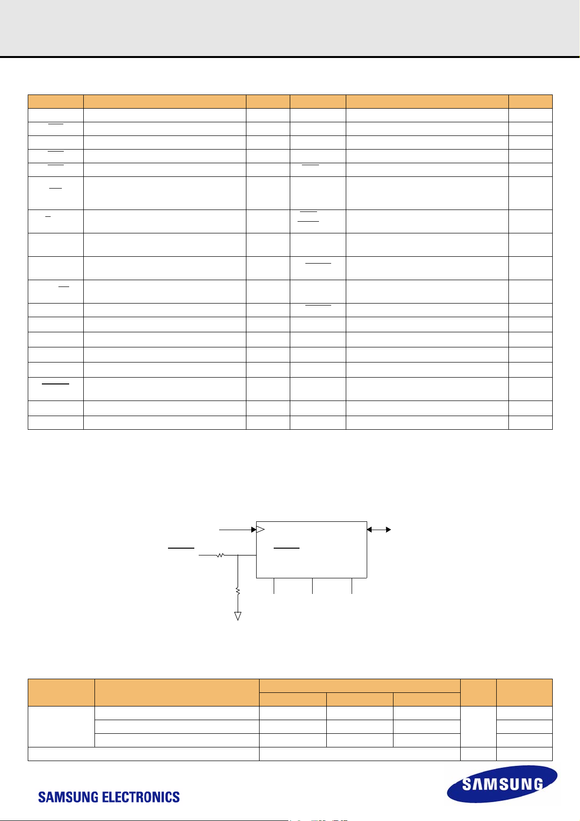
6. ON DIMM Thermal Sensor
SCL
EVENT
R1
0 Ω
NOTE : 1. All Samsung RDIMM support Thermal sensor on DIMM
2. When the SPD and the thermal sensor are placed on the module, R1 is placed but R2 is not.
When only the SPD is placed on the module, R2 is placed but R1 is not.
[ Table 1 ] Temperature Sensor Characteristics
Grade Range
75 < Ta < 95 - +/- 0.5 +/- 1.0
B
40 < Ta < 125 - +/- 1.0 +/- 2.0 -
-20 < Ta < 125 - +/- 2.0 +/- 3.0 -
Resolution 0.25 °C /LSB -
WP/EVENT
SA0 SA1 SA2
R2
0 Ω
SA0 SA1 SA2
Min. Typ . Max.
Temperature Sensor Accuracy
SDA
Units NOTE
-
°C
- 6 -

Rev. 1.0
http://www.BDTIC.com/SAMSUNG
Registered DIMM
datasheet DDR3L SDRAM
7. Input/Output Functional Description
Symbol Typ e Polarity Function
CK0 Input
CK0
CKE[1:0] Input Active High
S
[3:0] Input Active Low
ODT[1:0] Input Active High On-Die Termination control signals
AS, CAS, WE Input Active Low
R
V
REFDQ
V
REFCA
BA[2:0] Input
A[15:13,
12/BC,11,
10/AP,9:0]
DQ[63:0],
CB[7:0]
DM[8:0]
DQS[17:0] I/O Positive Edge Positive line of the differential data strobe for input and output data.
DQS
[17:0] I/O Negative Edge Negative line of the differential data strobe for input and output data.
TDQS[17:9],
[17:9] OUT
TDQS
SA[2:0] IN
SDA I/O
SCL IN
EVENT
V
DDSPD
RESET
Par_In IN Parity bit for the Address and Control bus. ("1 " : Odd, "0 ": Even)
Err_Out
TEST Used by memory bus analysis tools (unused (NC) on memory DIMMs)
Input
Supply Reference voltage for DQ0-DQ63 and CB0-CB7
Supply Reference voltage for A0-A15, BA0-BA2, RAS, CAS, WE, S0, S1, CKE0, CKE1, Par_In, ODT0 and ODT1.
Input
I/O Data and Check Bit Input/Output pins
OUT
(open
drain)
Supply
IN
OUT
(open
drain)
Positive
Edge
Negative
Edge
Active Low
Positive line of the differential pair of system clock inputs that drives input to the on-DIMM Clock Driver.
Negative line of the differential pair of system clock inputs that drives the input to the on-DIMM Clock Driver.
CKE HIGH activates, and CKE LOW deactivates internal clock signals, and device input buffers
and output drivers of the SDRAMs. Taking CKE LOW provides PRECHARGE POWER-DOWN
and SELF REFRESH operation (all banks idle), or ACTIVE POWER DOWN (row ACTIVE in any bank)
Enables the associated SDRAM command decoder when low and disables decoder when high.
When decoder is disabled, new commands are ignored and previous operations continue.
These input signals also disable all outputs (except CKE and ODT) of the register(s) on the DIMM when both
inputs are high. When both S[1:0] are high, all register outputs (except CKE, ODT and Chip select) remain in
the previous state. For modules supporting 4 ranks, S[3:2] operate similarly to S[1:0] for a second set of register outputs.
When sampled at the positive rising edge of the clock, CAS
cuted by the SDRAM.
Selects which SDRAM bank of eight is activated.
BA0 - BA2 define to which bank an Active, Read, Write or Precharge command is being applied. Bank
address also determines mode register is to be accessed during an MRS cycle.
Provided the row address for Active commands and the column address and Auto Precharge bit for Read/
Write commands to select one location out of the memory array in the respective bank. A10 is sampled during a Precharge command to determine whether the Precharge applies to one bank (A10 LOW) or all banks
(A10 HIGH). If only one bank is to be precharged, the bank is selected by BA. A12 is also utilized for BL 4/8
identification for "BL on the fly" during CAS command. The address inputs also provide the op-code during
Mode Register Set commands.
Active High Masks write data when high, issued concurrently with input data.
, VSS Supply Power and ground for the DDR SDRAM input buffers and core logic.
V
DD
Supply Termination Voltage for Address/Command/Control/Clock nets.
V
TT
TDQS/TDQS
enable the same termination resistance function on TDQS/TDQS
abled via mode register A11=0 in MR1, DM/TDQS will provide the data mask function and TDQS is not used.
X4/X16 DRAMs must disable the TDQS function via mode register A11=0 in MR1
These signals are tied at the system planar to either V
address range.
This bidirectional pin is used to transfer data into or out of the SPD EEPROM. A resistor must be
connected from the SDA bus line to V
This signal is used to clock data into and out of the SPD EEPROM. A resistor may be connected
from the SCL bus time to V
This signal indicates that a thermal event has been detected in the thermal sensing device.The system
should guarantee the electrical level requirement is met for the EVENT
Serial EEPROM positive power supply wired to a separate power pin at the connector which supports from
3.0 Volt to 3.6 Volt (nominal 3.3V) operation.
The RESET
low, all register outputs will be driven low and the Clock Driver clocks to the DRAMs and register(s) will be set
to low level (the Clock Driver will remain synchronized with the input clock)
Parity error detected on the Address and Control bus. A resistor may be connected from Err_Out
bus line to VDD on the system planar to act as a pull up.
is applicable for X8 DRAMs only. When enabled via Mode Register A11=1 in MR1, DRAM will
on the system planar to act as a pull-up.
DDSPD
on the system planar to act as a pull-up.
DDSPD
pin is connected to the RESET pin on the register and to the RESET pin on the DRAM. When
, RAS, and WE define the operation to be exe-
that is applied to DQS/DQS. When dis-
SS
or V
to configure the serial SPD EEPROM
DDSPD
pin on TS/SPD part.
- 7 -

Rev. 1.0
http://www.BDTIC.com/SAMSUNG
Registered DIMM
datasheet DDR3L SDRAM
8. Pinout Comparison Based On Module Type
Pin
48, 49
120, 240
53 Err_Out
63 NC
64 NC CK1
68 Par_In Connected to the register on all RDIMMs NC Not used on RDIMMs
76 S
77 ODT1, NC
79 S
167 NC TEST input used only on bus analysis probes NC
169 CKE1
171 A15
172 A14 A14
196 A13 A13
198 S
39, 40, 45, 46,
158, 159, 164,
165
125, 134, 143,
152, 161, 203,
212, 221, 230
126, 135, 144,
153, 162, 204,
213, 222, 231
187
NOTE : NC = No internal Connection
Signal NOTE Signal NOTE
V
TT
V
TT
1 Connected to the register on all RDIMMs S1
2, NC
3, NC
CBn Used on all RDIMMs; (n = 0...7) NC, CBn
DQSn,
TDQSn
DQS
TDQS
EVENT
NC
Additional connection for Termination Voltage for
Address/Command/Control/Clock nets.
Termination Voltage for Address/Command/Control/Clock nets.
Connected to the register on all RDIMMs NC Not
used on UDIMMs
Not used on RDIMMs
Connected to the register on dual- and quadrank
RDIMMs; NC on single-rank RDIMMs
Connected to the register on quad-rank
RDIMMs, not connected on single or dual rank
RDIMMs
Connected to the register on dual- and quadrank
RDIMMs; NC on single-rank RDIMMs
Connected to the register on all RDIMMs
Connected to the register on quad-rank
RDIMMs, not connected on single-or dual-rank
RDIMMs
Connected to DQS on x4 SDRAMs,
TDQS on x8 SDRAMs on RDIMMs; (n = 9...17)
n,
Connected to DQS
SDRAMs on RDIMMs; (n=9...17)
n
Connected to optional thermal sensing component.
NC on Modules without a thermal sensing
component.
RDIMM UDIMM
NC Not used on UDIMMs
Termination Voltage for Address/Command/Control/Clock nets.
Used for 2 rank UDIMMs, not used on single-rank
UDIMMs, but terminated
Used for dual-rank UDIMMs, not connected
on single-rank UDIMMs
Used for dual-rank UDIMMs, not connected
on single-rank UDIMMs
TEST input used only on bus analysis
probes
Used for dual-rank UDIMMs, not connected
on single-rank UDIMMs
connected to SDRAMs on UDIMMs. However,
these signals are terminated on
UDIMMs. A15 not routed on some RCs
Used on x72 UDIMMs, (n = 0...7); not
used on x64 UDIMMs
Connected to DM on x8 DRAMs, UDM or
LDM on x16 DRAMs on UDIMMs;
(n = 0...8)
on x4 DRAMs, TDQS on x8
V
TT
NC NC Not used on UDIMMs
CK1
ODT1,NC
NC Not used on UDIMMs
CKE1,
NC
A15, NC Depending on device density, may not be
NC Not used on UDIMMs
DMn
NC Not used on UDIMMs
NC Not used on UDIMMs
- 8 -
Rev. 1.0
http://www.BDTIC.com/SAMSUNG
Registered DIMM
datasheet DDR3L SDRAM
9. Registering Clock Driver Specification
9.1 Timing & Capacitance values
TC = TBD
V
= 1.35V(1.28V~1.45V)
Symbol Parameter Conditions
fclock Input Clock Frequency application frequency 300 670 MHz
t
C
IN
C
IN
C
CH/tCL
t
ACT
t
SU
t
H
t
PDM
t
DIS
t
EN
(DATA)
(CLOCK)
(RST)
IN
Pulse duration, CK, CK HIGH or LOW 0.4 -
Inputs active time4 before RESET is taken HIGH
Setup time Input valid before CK/CK 100 - ps
Hold time
Propagation delay, single-bit switching CK/CK to output 0.65 1.0 ns
output disable time(1/2-Clock pre-launch)
output disable time(3/4-Clock pre-launch) 0.25 -
output enable time(1/2-Clock pre-launch)
output enable time(3/4-Clock pre-launch) - 0.25
Data Input Capacitance 1.5 2.5
Data Input Capacitance 2 3
Reset Input Capacitance - 3
DCKE0/1 = LOW and
DCS0/1
= HIGH
Input to remain Valid after CK/
CK
CK/CK
to output float
CK/CK
to output driving
DD
& 1.5V(1.425~1.575V)
Min Max
8-
175 -
0.5 -
-0.5
Units Notes
t
CK
t
CK
t
CK
t
CK
pF
9.2 Clock driver Characteristics
Symbol Parameter Conditions
(cc)
t
jit
t
t
t
jit
t
jit
t
t
t
STAB
t
fdyn
CKsk
(per)
(hper)
Qsk1
Qsk1
dynoff
Cycle-to-cycle period jitter 0 40 ps
Stabilization time -6us
Dynamic phase offset -50 50 ps
Clock Output skew 50 ps
Yn Clock Period jitter -40 40 ps
Half period jitter -50 50 ps
Qn Output to clock tolerance (Standard 1/2 -Clock
Pre-Launch)
Output clock tolerance (3/4 Clock Pre-Launch)
Maximum re-driven dynamic clock off-set -80 80 ps
Output Inversion enabled -100 200
OUtput Inversion disabled -100 300
Output Inversion enabled -100 200
OUtput Inversion disabled -100 300
TC = TBD
= 1.35V(1.28V~1.45V)
V
DD
& 1.5V(1.425~1.575V)
Min Max
Units Notes
ps
ps
- 9 -

Rev. 1.0
http://www.BDTIC.com/SAMSUNG
Registered DIMM
datasheet DDR3L SDRAM
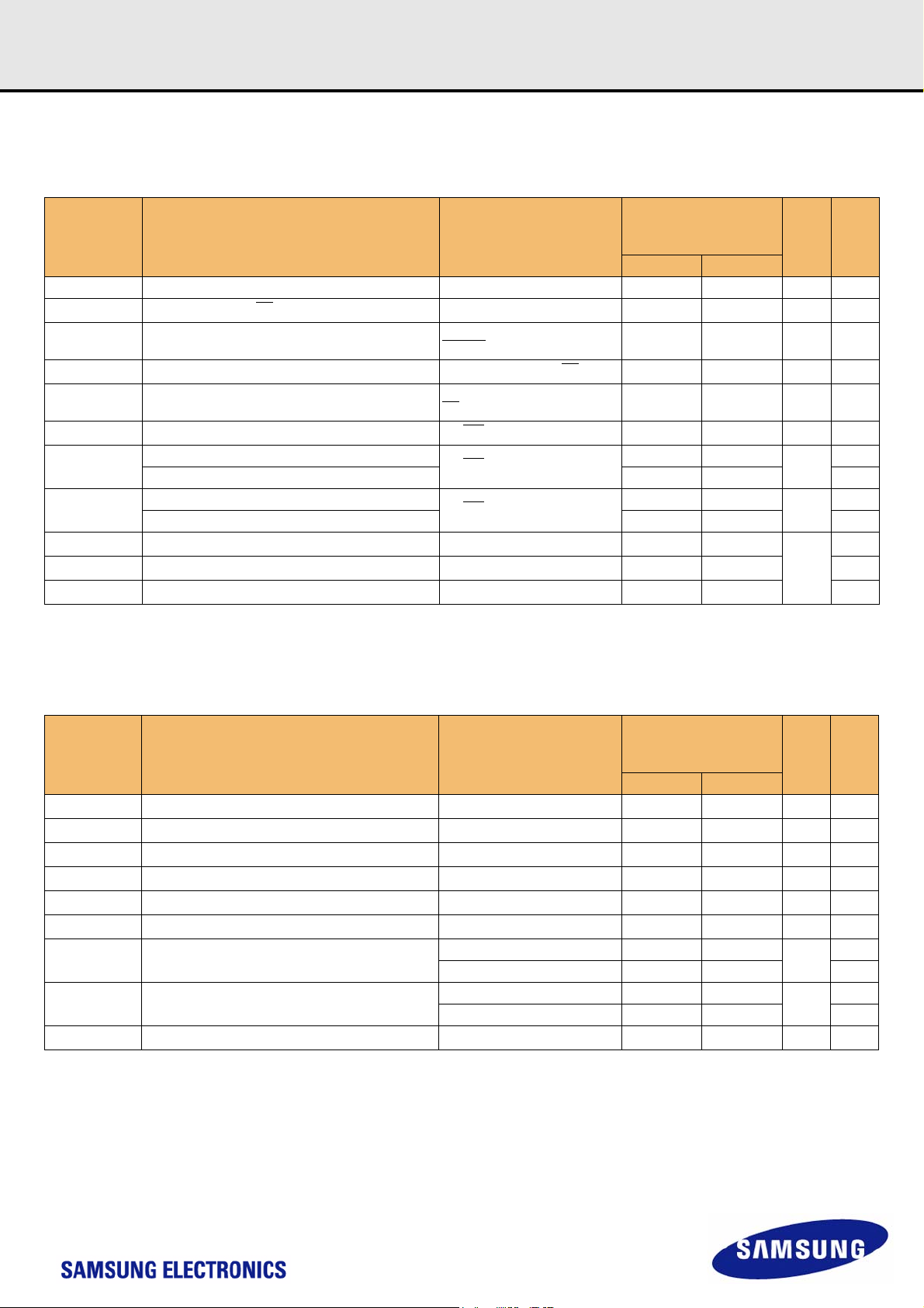
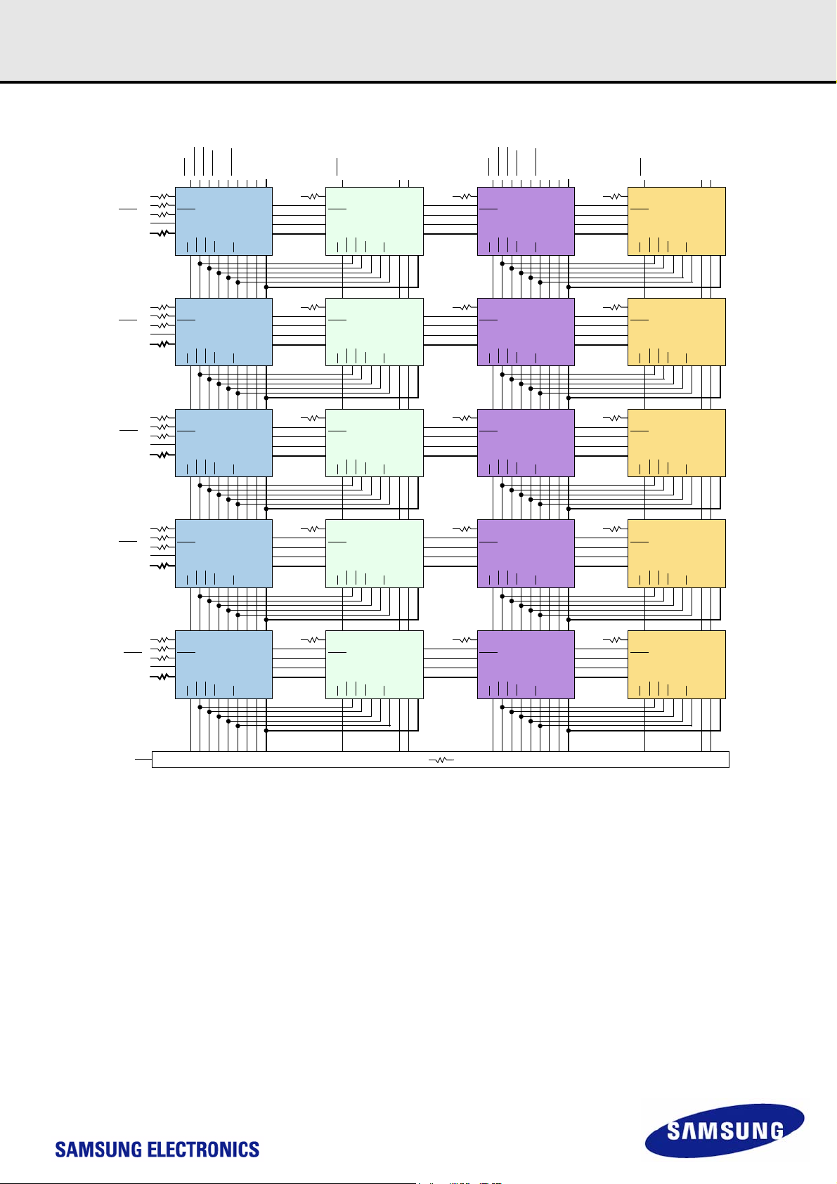
10. Function Block Diagram:
10.1 16GB, 2Gx72 Module (Populated as 2 ranks of x4 DDR3 SDRAMs)
RS0A
RRASA
RCASA
RWEA
PCK0A
PCK0A
RCKE0A
RODT0A
A[N:0]A
DQS17
DQS17
VSS
CB[7:4]
DQS12
DQS12
VSS
DQ[31:28]
DQS11
DQS11
VSS
DQ[23:20]
DQS
DQS
DM
DQ[3:0]
CS
DQS
DQS
DM
DQ[3:0]
CS
DQS
DQS
DM
DQ[3:0]
CS
D17
RAS
CASWECKCKCKE
D12
RAS
CASWECKCKCKE
D11
RAS
CASWECKCKCKE
ODT
ODT
ODT
/BA[N:0]A
A[N:0]/BA[N:0]
A[N:0]/BA[N:0]
A[N:0]/BA[N:0]
RS1A
DQS
DQS
DM
DQ[3:0]
CS
DQS
DQS
DM
DQ[3:0]
CS
DQS
DQS
DM
DQ[3:0]
CS
PCK1A
D35
RAS
CASWECKCKCKE
D30
RAS
CASWECKCKCKE
D29
RAS
CASWECKCKCKE
PCK1A
RCKE1A
RODT1A
ODT
ODT
ODT
RS0A
DQS17
DQS17
VSS
CB[3:0]
A[N:0]/BA[N:0]
DQS12
DQS12
VSS
DQ[27:24]
A[N:0]/BA[N:0]
DQS11
DQS11
VSS
DQ[19:16]
A[N:0]/BA[N:0]
DQS
DQS
DM
DQ[3:0]
CS
DQS
DQS
DM
DQ[3:0]
CS
DQS
DQS
DM
DQ[3:0]
CS
RRASA
RCASA
RWEA
PCK0A
D8
RAS
CASWECKCKCKE
D3
RAS
CASWECKCKCKE
D2
RAS
CASWECKCKCKE
PCK0A
RCKE0A
RODT0A
ODT
ODT
ODT
A[N:0]A
/BA[N:0]A
A[N:0]/BA[N:0]
A[N:0]/BA[N:0]
A[N:0]/BA[N:0]
RS1A
DQS
DQS
DM
DQ[3:0]
CS
DQS
DQS
DM
DQ[3:0]
CS
DQS
DQS
DM
DQ[3:0]
CS
PCK1A
D26
RAS
CASWECKCKCKE
D21
RAS
CASWECKCKCKE
D20
RAS
CASWECKCKCKE
PCK1A
RCKE1A
RODT1A
ODT
ODT
ODT
A[N:0]/BA[N:0]
A[N:0]/BA[N:0]
A[N:0]/BA[N:0]
DQS10
DQS10
VSS
DQ[15:12]
DQS0
DQS0
VSS
DQ[3:0]
DQS
DQS
DM
D10
DQ[3:0]
CS
RAS
CASWECKCKCKE
DQS
DQS
DM
DQ[3:0]
CS
RAS
CASWECKCKCKE
Vtt
ODT
D0
ODT
A[N:0]/BA[N:0]
A[N:0]/BA[N:0]
DQS
DQS
DM
DQ[3:0]
CS
DQS
DQS
DM
DQ[3:0]
CS
D28
RAS
CASWECKCKCKE
D18
RAS
CASWECKCKCKE
ODT
ODT
A[N:0]/BA[N:0]
A[N:0]/BA[N:0]
DQS10
DQS10
VSS
DQ[11:8]
DQS0
DQS0
VSS
DQ[7:4]
DQS
DQS
DM
D1
DQ[3:0]
CS
RAS
CASWECKCKCKE
DQS
DQS
DM
DQ[3:0]
CS
RAS
CASWECKCKCKE
Vtt
ODT
D9
ODT
A[N:0]/BA[N:0]
A[N:0]/BA[N:0]
DQS
DQS
DM
DQ[3:0]
CS
DQS
DQS
DM
DQ[3:0]
CS
D19
RAS
CASWECKCKCKE
D27
RAS
CASWECKCKCKE
ODT
ODT
A[N:0]/BA[N:0]
A[N:0]/BA[N:0]
- 10 -
Rev. 1.0
http://www.BDTIC.com/SAMSUNG
Registered DIMM
RS0B
DQS14
DQS14
VSS
CB[47:44]
DQS4
DQS4
VSS
DQ[35:32]
DQS16
DQS16
VSS
DQ[63:60]
DQS
DQS
DM
DQ[3:0]
CS
DQS
DQS
DM
DQ[3:0]
CS
DQS
DQS
DM
DQ[3:0]
CS
RRASB
RCASB
RWEB
PCK0B
D14
RAS
CASWECKCKCKE
D4
RAS
CASWECKCKCKE
D16
RAS
CASWECKCKCKE
datasheet DDR3L SDRAM
PCK0B
RCKE0B
RODT0B
A[N:0]B
ODT
ODT
ODT
/BA[N:0]B
A[N:0]/BA[N:0]
A[N:0]/BA[N:0]
A[N:0]/BA[N:0]
RS1B
DQS
DQS
DM
DQ[3:0]
CS
DQS
DQS
DM
DQ[3:0]
CS
DQS
DQS
DM
DQ[3:0]
CS
PCK1B
D32
RAS
CASWECKCKCKE
D22
RAS
CASWECKCKCKE
D34
RAS
CASWECKCKCKE
PCK1B
RCKE1B
RODT1B
ODT
ODT
ODT
DQS13
DQS13
VSS
CB[39:36]
A[N:0]/BA[N:0]
DQS5
DQS5
VSS
DQ[43:40]
A[N:0]/BA[N:0]
DQS15
DQS15
VSS
DQ[55:52]
A[N:0]/BA[N:0]
RS0B
DQS
DQS
DM
DQ[3:0]
CS
DQS
DQS
DM
DQ[3:0]
CS
DQS
DQS
DM
DQ[3:0]
CS
RRASB
RCASB
RWEB
PCK0B
D13
RAS
CASWECKCKCKE
D5
RAS
CASWECKCKCKE
D15
RAS
CASWECKCKCKE
PCK0B
RCKE0B
RODT0B
A[N:0]B
ODT
ODT
ODT
/BA[N:0]B
A[N:0]/BA[N:0]
A[N:0]/BA[N:0]
A[N:0]/BA[N:0]
RS1B
DQS
DQS
DM
DQ[3:0]
CS
DQS
DQS
DM
DQ[3:0]
CS
DQS
DQS
DM
DQ[3:0]
CS
PCK1B
D31
RAS
CASWECKCKCKE
D23
RAS
CASWECKCKCKE
D33
RAS
CASWECKCKCKE
PCK1B
RCKE1B
RODT1B
ODT
A[N:0]/BA[N:0]
ODT
A[N:0]/BA[N:0]
ODT
A[N:0]/BA[N:0]
DQS10
DQS10
VSS
DQ[59:56]
DQS
DQS
DM
DQ[3:0]
CS
D7
RAS
CASWECKCKCKE
ODT
DQS
DQS
DM
D25
DQ[3:0]
A[N:0]/BA[N:0]
CS
RAS
CASWECKCKCKE
ODT
A[N:0]/BA[N:0]
DQ[51:48]
Vtt
Integrated Thermal sensor in SPD
SCL
EVENT EVENT
A0
A1 A2
SDA
SA0 SA1 SA2
Serial PD w/ integrated Thermal sensor
V
DDSPD
V
DD
V
TT
V
REFCA
V
REFDQ
V
SS
NOTE:
1. See wiring diagrams for resistor values.
Serial PD
D0 - D35
D0 - D35
D0 - D35
D0 - D35
2. ZQ pins of each SDRAM are connected to individual RZQ resistors (240 +/-1%)ohms...
DQS6
DQS6
VSS
DQS
DQS
DM
DQ[3:0]
CS
D6
RAS
CASWECKCKCKE
ODT
DQS
DQS
DM
D24
DQ[3:0]
A[N:0]/BA[N:0]
CS
RAS
CASWECKCKCKE
ODT
A[N:0]/BA[N:0]
Vtt
RS0A -> CS0 : SDRAMs D[3:0], D[12:0], D17
RS0B -> CS0 : SDRAMs D[7:4], D[16:13]
1A -> CS1 : SDRAMs D[21:18], D[30:26], D35
RS
1B -> CS1 : SDRAMs D[25:22], D[34:31]
RS
RBA[N:0]A -> BA[N:0]: SDRAMs D[3:0], D[12:8], D[21:17], D[30:26], D35
RBA[N:0]B -> BA[N:0]: SDRAMs D[7:4], D[16:13], D[25:22], D[34: 31]
RA[N:0]A -> A[N:0]: SDRAMs D[3:0], D[12:8], D[21:17], D[30:26], D35
RA[N:0]B -> A[N:0]: SDRAMs D[7:4], D[16:13], D[25:22], D[34:31]
A -> RAS: SDRAMs D[3:0], D[12:8], D[21:17], D[30:26], D35
RRAS
B -> RAS: SDRAMs D[7:4], D[16:13], D[25:22], D[34:31]
RRAS
RCAS
A -> CAS: SDRAMs D[4:0], D8, D[13:9], D[22:18], D[31:27]
B -> CAS: SDRAMs D[8:5], D[17:14], D[26:23], D[35:32]
RCAS
1:2
RWE
R
E
G
S
T
E
R
Ω
RST
A -> WE: SDRAMs D[4:0], D8, D[13:9], D[22:18], D[31:27]
B -> WE: SDRAMs D[8:5], D[17:14], D[26:23], D[35:32]
RWE
RCKE0A -> CKE0: SDRAMs D[3:0], D[12:8], D17
RCKE0B -> CKE0: SDRAMs D[7:4], D[16:13]
I
RCKE1A -> CKE1: SDRAMs D[21:18], D[30:26], D35
RCKE1B -> CKE1: SDRAMs D[25:22], D[34:31]
RODT0A -> ODT0: SDRAMs D[3:0], D[12:8], D17
RODT0B -> ODT0: SDRAMs D[7:4], D[16:13]
RODT1A -> ODT1: SDRAMs D[21:18], D[30:26], D35
RODT1B -> ODT1: SDRAMs D[25:22], D[34:31]
PCK0A -> CK: SDRAMs D[3:0], D[12:8], D17
PCK0B -> CK: SDRAMs D[7:4], D[16:13]
PCK1A -> CK: SDRAMs D[21:18], D[30:26], D35
PCK1B -> CK: SDRAMs D[25:22], D[34:31]
A -> CK: SDRAMs D[3:0], D[12:8], D17
PCK0
B -> CK: SDRAMs D[7:4], D[16:13]
PCK0
PCK1
A -> CK: SDRAMs D[21:18], D[30:26], D35
B -> CK: SDRAMs D[25:22], D[34:31]
PCK1
ERR_OUT
RST : SDRAMs D[35:0]
BA[N:0]
A[N:0]
RAS
CAS
WE
CKE0
CKE1
ODT0
ODT1
S0
S1
CK0
CK0
CK0
CK0
PAR_IN
RESET
120
±
3%
- 11 -
Rev. 1.0
http://www.BDTIC.com/SAMSUNG
Registered DIMM
datasheet DDR3L SDRAM
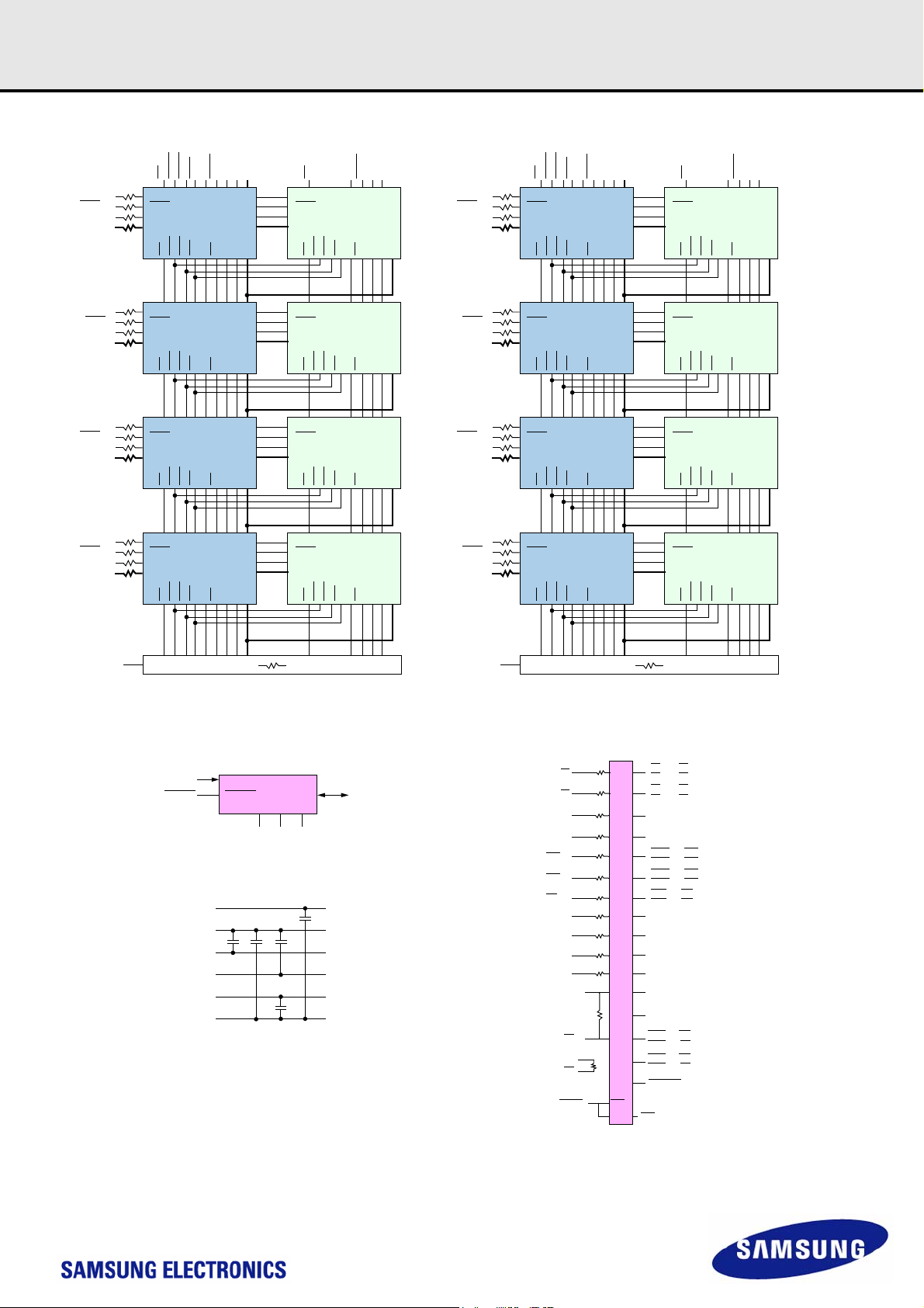
10.2 16GB, 2Gx72 Module (Populated as 4 ranks of x8 DDR3 SDRAMs)
PCK0
CS0
PCK0
WCKE0
DQS0
DQS0
DQ[7:0]
DQS1
DQS1
DQ[15:8]
DQS2
DQS2
DQ[23:16]
DQS3
DQS3
DQ[31:24]
DQS8
DQS8
CB[7:0]
WODT0
CKCSCK
CKE
CKCSCK
CKCSCK
CKCSCK
CKCSCK
ODT
U0
CKE
ODT
U1
CKE
ODT
U2
CKE
ODT
U3
CKE
ODT
U4
DQS
DQS
DQ[7:0]
ZQ
DQS
DQS
DQ[7:0]
ZQ
DQS
DQS
DQ[7:0]
ZQ
DQS
DQS
DQ[7:0]
ZQ
DQS
DQS
DQ[7:0]
ZQ
Vtt
CS1
DQS
DQS
DQ[7:0]
ZQ
DQS
DQS
DQ[7:0]
ZQ
DQS
DQS
DQ[7:0]
ZQ
DQS
DQS
DQ[7:0]
ZQ
DQS
DQS
DQ[7:0]
ZQ
PCK0
PCK0
CKCSCK
CKCSCK
CKCSCK
CKCSCK
CKCSCK
U9
U10
U11
U12
U13
WCKE1
CKE
CKE
CKE
CKE
CKE
VDD
ODT
ODT
ODT
ODT
ODT
DQS
DQS
DQ[7:0]
ZQ
DQS
DQS
DQ[7:0]
ZQ
DQS
DQS
DQ[7:0]
ZQ
DQS
DQS
DQ[7:0]
ZQ
DQS
DQS
DQ[7:0]
ZQ
CS2
PCK2
PCK2
CKCSCK
CKCSCK
CKCSCK
CKCSCK
CKCSCK
U18
U19
U20
U21
U22
WCKE0
CKE
CKE
CKE
CKE
CKE
WODT1
ODT
ODT
ODT
ODT
ODT
CS3
DQS
DQS
DQ[7:0]
ZQ
DQS
DQS
DQ[7:0]
ZQ
DQS
DQS
DQ[7:0]
ZQ
DQS
DQS
DQ[7:0]
ZQ
DQS
DQS
DQ[7:0]
ZQ
PCK2
PCK2
CKCSCK
CKCSCK
CKCSCK
CKCSCK
CKCSCK
U27
U28
U29
U30
U31
WCKE1
CKE
CKE
CKE
CKE
CKE
VDD
ODT
ODT
S0 RS0-> CS0 : SDRAMs D[8:0]
S1 RS1-> CS1 : SDRAMs D[17:9]
S2
S3
BA[N:0]
A[N:0]
ODT
RAS
CAS
WE
CKE0
CKE1
ODT
ODT0
ODT1
CK0
ODT
CK0
PAR_IN
RESET
RS
2-> CS2 : SDRAMs D[26:18]
RS
3-> CS3 : SDRAMs D[35:27]
WBA[N:0] -> BA[N:0]: SDRAMs D[4:0], D8, D[13:9], D[22:18], D[31:27 ]
EBA[N:0] -> BA[N:0]: SDRAMs D[8:5], D[17:14], D[26:23], D[35:32]
WA[N:0] -> A[N:0]: SDRAMs D[4:0], D8, D[13:9], D[22:18], D[31:27]
EA[N:0] -> A[N:0]: SDRAMs D[8:5], D[17:14], D[26:23], D[35:32]
-> RAS: SDRAMs D[4:0], D8, D[13:9], D[22:18], D[31:27]
WRAS
-> RAS: SDRAMs D[8:5], D[17:14], D[26:23], D[35:32]
ERAS
WCAS
-> CAS: SDRAMs D[4:0], D8, D[13:9], D[22:18], D[31:27]
-> CAS: SDRAMs D[8:5], D[17:14], D[26:23], D[35:32]
ECAS
1:2
WWE
-> WE: SDRAMs D[4:0], D8, D[13:9], D[22:18], D[31:27]
-> WE: SDRAMs D[8:5], D[17:14], D[26:23], D[35:32]
EWE
WCKE0 -> CKE0: SDRAMs D[4:0], D[22:18]
ECKE0 -> CKE0: SDRAMs D[8:5], D[26:23]
WCKE1 -> CKE1: SDRAMs D[13:9], D[31:27]
ECKE1 -> CKE1: SDRAMs D[17:14], D[35:32]
WODT0 -> ODT0: SDRAMs D[4:0]
EODT0 -> ODT0: SDRAMs D[8:5]
WODT1 -> ODT1: SDRAMs D[22:18]
EODT1 -> ODT1: SDRAMs D[26:23]
PCK0 -> CK: SDRAMs D[4:0], D[13:9]
PCK1 -> CK: SDRAMs D[8:5], D[26:23]
PCK2 -> CK: SDRAMs D[22:18], D[31:27]
PCK3 -> CK: SDRAMs D[17:14], D[35:32]
PCK0
-> CK: SDRAMs D[4:0], D[13:9]
-> CK: SDRAMs D[8:5], D[26:23]
PCK1
PCK2 -> CK: SDRAMs D[22:18], D[31:27]
-> CK: SDRAMs D[17:14], D[35:32]
PCK3
Err_out
RST : SDRAMs D[35:0]
RST
R
E
G
I
S
T
E
R
QERR
DQS4
DQS4
DQ[39:32]
DQS5
DQS5
DQ[47:40]
DQS6
DQS6
DQ[55:48]
DQS3
DQS3
DQ[31:24]
Thermal sensor with SPD
CS0
DQS
DQS
DQ[7:0]
ZQ
DQS
DQS
DQ[7:0]
ZQ
DQS
DQS
DQ[7:0]
ZQ
DQS
DQS
DQ[7:0]
ZQ
PCK1
PCK1
CKCSCK
CKCSCK
CKCSCK
CKCSCK
SCL
ECKE0
EODT0
CKE
ODT
U5
CKE
ODT
U6
CKE
ODT
U7
CKE
ODT
U8
CS1
DQS
DQS
DQ[7:0]
ZQ
DQS
DQS
DQ[7:0]
ZQ
DQS
DQS
DQ[7:0]
ZQ
DQS
DQS
DQ[7:0]
ZQ
PCK1
PCK1
CKCSCK
CKCSCK
CKCSCK
CKCSCK
U14
U15
U16
U17
ECKE1
CKE
CKE
CKE
CKE
VDD
ODT
ODT
ODT
ODT
DQS
DQS
DQ[7:0]
ZQ
DQS
DQS
DQ[7:0]
ZQ
DQS
DQS
DQ[7:0]
ZQ
DQS
DQS
DQ[7:0]
ZQ
CS2
PCK3
PCK3
CKCSCK
CKCSCK
CKCSCK
CKCSCK
U23
U24
U25
U26
ECKE0
CKE
CKE
CKE
CKE
EODT1
ODT
ODT
ODT
ODT
CS3
DQS
DQS
DQ[7:0]
ZQ
DQS
DQS
DQ[7:0]
ZQ
DQS
DQS
DQ[7:0]
ZQ
DQS
DQS
DQ[7:0]
ZQ
PCK3
PCK3
CKCSCK
CKCSCK
CKCSCK
CKCSCK
U32
U33
U34
U35
ECKE1
CKE
CKE
CKE
CKE
VDD
ODT
ODT
ODT
ODT
EVENT EVENT
A0
A1 A2
SA0 SA1 SA2
V
DDSPD
V
DD
V
TT
V
REFCA
V
REFDQ
V
SS
NOTE :
1. Unless otherwise noted, resistor values are 15Ω ± 5%.
2. See the wiring diagrams for all resistors associated with the command, address and control bus.
3. ZQ resistors are 240Ω ± 1% . For all other resistor values refer to
the appropriate wiring diagram.
SDA
Serial PD
D0 - D35
D0 - D35
D0 - D35
D0 - D35
Vtt
- 12 -
Rev. 1.0
http://www.BDTIC.com/SAMSUNG
Registered DIMM
datasheet DDR3L SDRAM
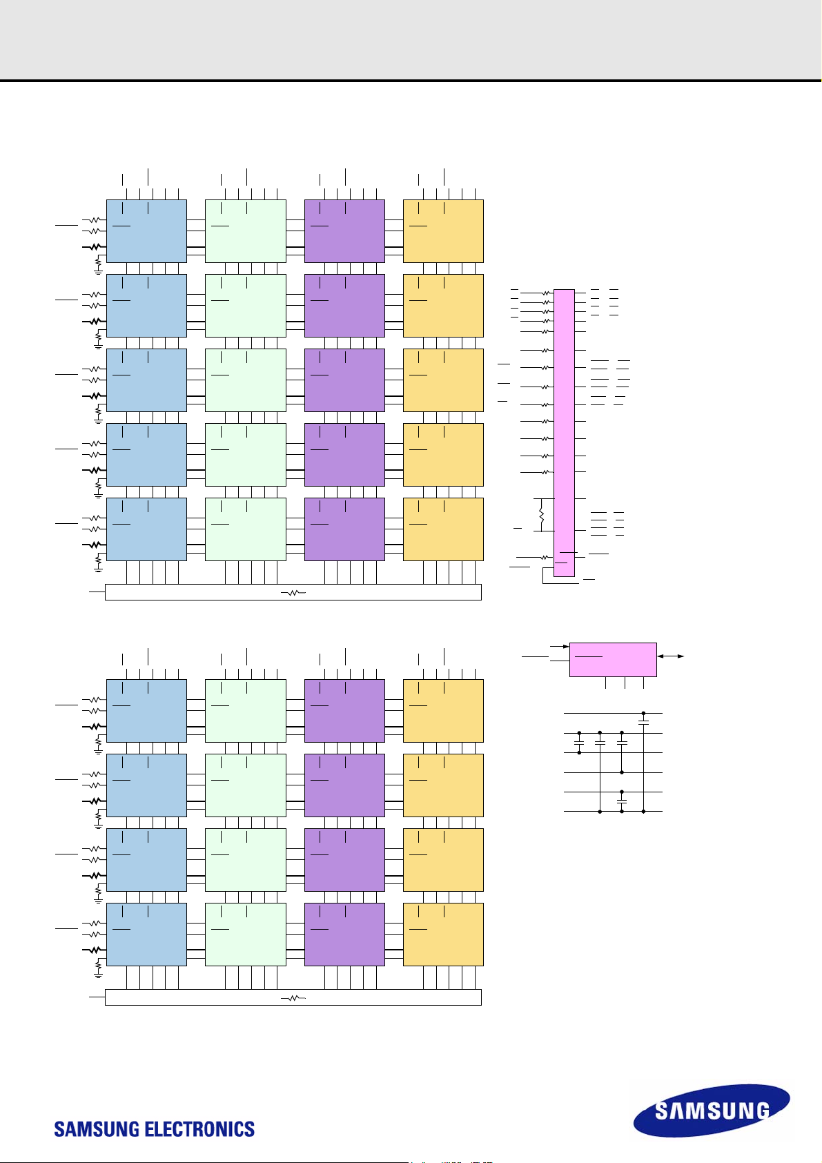
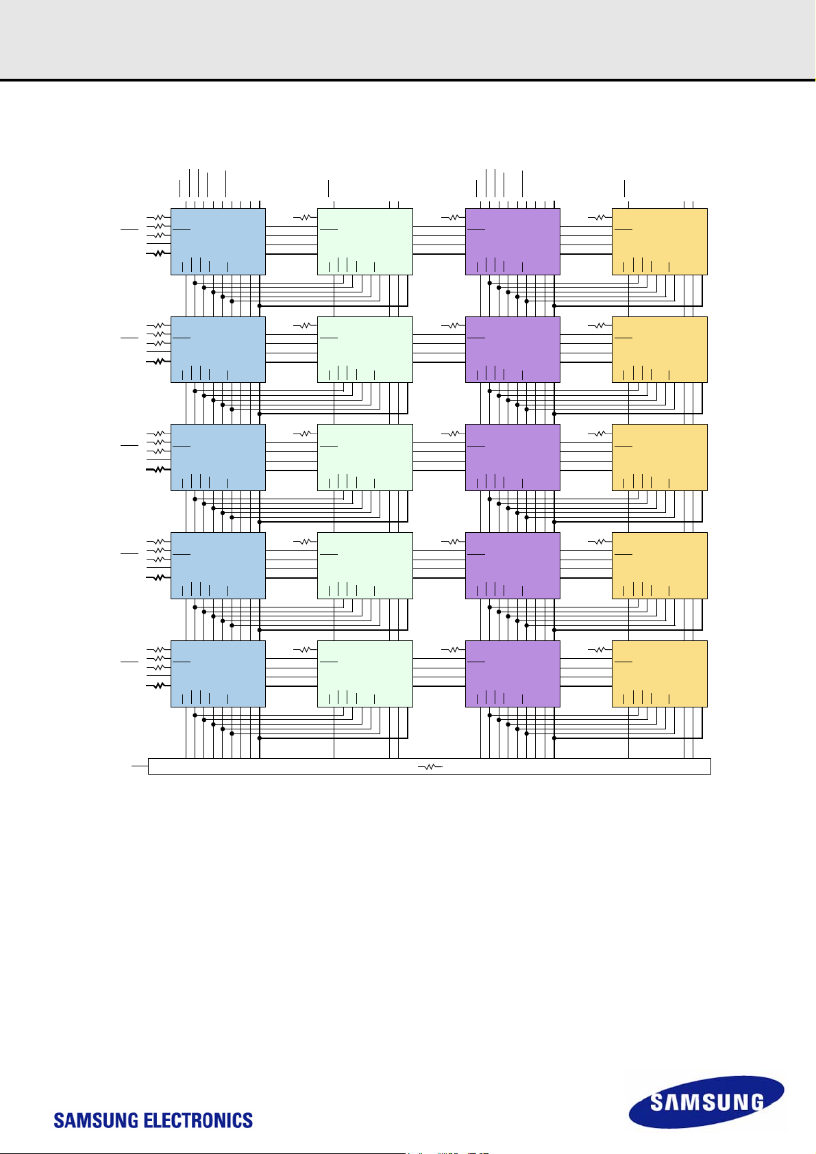
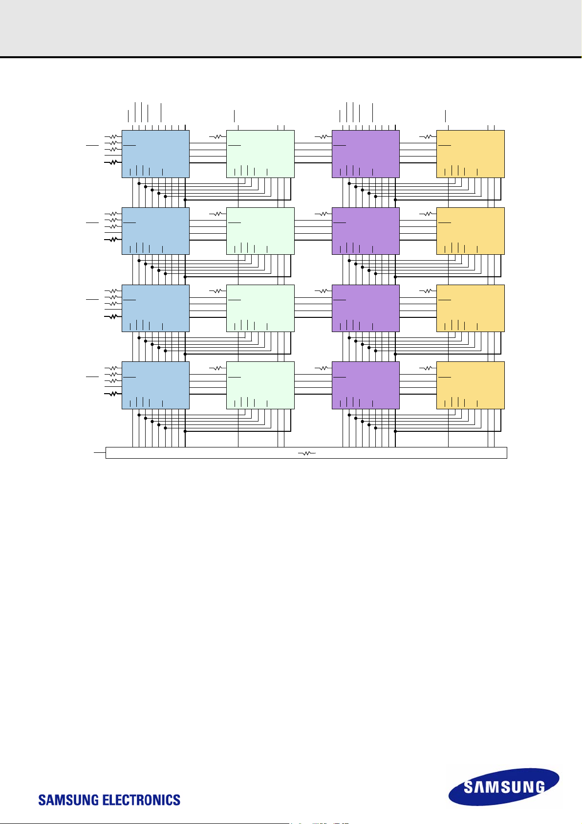
10.3 32GB, 4Gx72 Module (Populated as 4 ranks of x4 DDR3 SDRAMs)
ARS0A
ARRASA
ARCASA
ARWEA
APCK0A
APCK0A
ARCKE0A
ARODT0A
ARA[N:0]A
VSS VSSZQ
DQS8
DQS8
VSS
CB[3:0]
VSS VSSZQ
DQS3
DQS3
VSS
DQ[27:24]
VSS VSSZQ
DQS2
DQS2
VSS
DQ[19:16]
DQS
DQS
DM
DQ[3:0]
CS
DQS
DQS
DM
DQ[3:0]
CS
DQS
DQS
DM
DQ[3:0]
CS
D9
RAS
CASWECKCKCKE
D7
RAS
CASWECKCKCKE
D5
RAS
CASWECKCKCKE
ODT
ODT
ODT
/ARBA[N:0]A
A[N:0]/BA[N:0]
A[N:0]/BA[N:0]
A[N:0]/BA[N:0]
ARS1A
ZQ
DQS
DQS
DM
DQ[3:0]
CS
ZQ
DQS
DQS
DM
DQ[3:0]
CS
ZQ
DQS
DQS
DM
DQ[3:0]
CS
D8
RAS
CASWECKCKCKE
D6
RAS
CASWECKCKCKE
D4
RAS
CASWECKCKCKE
ARCKE1A
VDD
ODT
ODT
ODT
A[N:0]/BA[N:0]
A[N:0]/BA[N:0]
A[N:0]/BA[N:0]
BRS2A
DQS
DQS
DM
DQ[3:0]
CS
DQS
DQS
DM
DQ[3:0]
CS
DQS
DQS
DM
DQ[3:0]
CS
BRRASA
BRCASA
BRWEA
D45
RAS
CASWECKCKCKE
D47
RAS
CASWECKCKCKE
D49
RAS
CASWECKCKCKE
BPCK0A
BPCK0A
BRCKE0A
BRODT1A
BRA[N:0]A
ODT
ODT
ODT
/BRBA[N:0]A
VSSZQ
A[N:0]/BA[N:0]
VSSZQ
A[N:0]/BA[N:0]
VSSZQ
A[N:0]/BA[N:0]
ZQVSS
DQS
DQS
DM
DQ[3:0]
CS
ZQVSS
DQS
DQS
DM
DQ[3:0]
CS
ZQVSS
DQS
DQS
DM
DQ[3:0]
CS
BRS3A
RAS
RAS
RAS
D44
CASWECKCKCKE
D46
CASWECKCKCKE
D48
CASWECKCKCKE
BRCKE1A
VDD
ODT
A[N:0]/BA[N:0]
ODT
A[N:0]/BA[N:0]
ODT
A[N:0]/BA[N:0]
VSS VSSZQ
DQS1
DQS1
VSS
DQ[11:8]
VSS VSSZQ
DQS0
DQS0
VSS
DQ[3:0]
Vtt
DQS
DQS
DM
DQ[3:0]
CS
DQS
DQS
DM
DQ[3:0]
CS
D3
RAS
CASWECKCKCKE
D1
RAS
CASWECKCKCKE
ODT
ODT
ZQ
DQS
DQS
DM
D2
DQ[3:0]
A[N:0]/BA[N:0]
A[N:0]/BA[N:0]
CS
ZQ
DQS
DQS
DM
DQ[3:0]
CS
RAS
CASWECKCKCKE
D0
RAS
CASWECKCKCKE
ODT
ODT
A[N:0]/BA[N:0]
A[N:0]/BA[N:0]
DQS
DQS
DM
DQ[3:0]
CS
DQS
DQS
DM
DQ[3:0]
CS
D51
RAS
CASWECKCKCKE
D53
RAS
CASWECKCKCKE
ODT
ODT
VSSZQ
A[N:0]/BA[N:0]
VSSZQ
A[N:0]/BA[N:0]
ZQVSS
DQS
DQS
DM
DQ[3:0]
CS
ZQVSS
DQS
DQS
DM
DQ[3:0]
CS
D50
RAS
CASWECKCKCKE
D52
RAS
CASWECKCKCKE
ODT
ODT
A[N:0]/BA[N:0]
A[N:0]/BA[N:0]
- 13 -
Rev. 1.0
http://www.BDTIC.com/SAMSUNG
Registered DIMM
VSS VSSZQ
DQS17
DQS17
VSS
CB[7:4]
VSS VSSZQ
DQS12
DQS12
VSS
DQ[31:28]
VSS VSSZQ
DQS11
DQS11
VSS
DQ[23:20]
ARS0A
DQS
DQS
DM
DQ[3:0]
CS
DQS
DQS
DM
DQ[3:0]
CS
DQS
DQS
DM
DQ[3:0]
CS
ARRASA
ARCASA
ARWEA
APCK0A
D27
RAS
CASWECKCKCKE
D25
RAS
CASWECKCKCKE
D23
RAS
CASWECKCKCKE
datasheet DDR3L SDRAM
APCK0A
ARCKE0A
ARODT0A
ARA[N:0]A
/ARBA[N:0]A
ODT
A[N:0]/BA[N:0]
ODT
A[N:0]/BA[N:0]
ODT
A[N:0]/BA[N:0]
ARS1A
ZQ
DQS
DQS
DM
DQ[3:0]
CS
ZQ
DQS
DQS
DM
DQ[3:0]
CS
ZQ
DQS
DQS
DM
DQ[3:0]
CS
D26
RAS
CASWECKCKCKE
D24
RAS
CASWECKCKCKE
D22
RAS
CASWECKCKCKE
ARCKE1A
VDD
ODT
A[N:0]/BA[N:0]
ODT
A[N:0]/BA[N:0]
ODT
A[N:0]/BA[N:0]
BRS2A
DQS
DQS
DM
DQ[3:0]
CS
DQS
DQS
DM
DQ[3:0]
CS
DQS
DQS
DM
DQ[3:0]
CS
BRRASA
BRCASA
BRWEA
BPCK0A
D63
RAS
CASWECKCKCKE
D65
RAS
CASWECKCKCKE
D67
RAS
CASWECKCKCKE
BPCK0A
BRCKE0A
BRODT1A
BRA[N:0]A
/BRBA[N:0]A
VSSZQ
ODT
A[N:0]/BA[N:0]
VSSZQ
ODT
A[N:0]/BA[N:0]
VSSZQ
ODT
A[N:0]/BA[N:0]
ZQVSS
DQS
DQS
DM
DQ[3:0]
CS
ZQVSS
DQS
DQS
DM
DQ[3:0]
CS
ZQVSS
DQS
DQS
DM
DQ[3:0]
CS
BRS3A
D62
RAS
CASWECKCKCKE
D64
RAS
CASWECKCKCKE
D66
RAS
CASWECKCKCKE
BRCKE1A
VDD
ODT
A[N:0]/BA[N:0]
ODT
A[N:0]/BA[N:0]
ODT
A[N:0]/BA[N:0]
VSS VSSZQ
DQS10
DQS10
VSS
DQ[15:12]
VSS VSSZQ
DQS9
DQS9
VSS
DQ[7:4]
Vtt
DQS
DQS
DM
DQ[3:0]
CS
DQS
DQS
DM
DQ[3:0]
CS
D21
RAS
CASWECKCKCKE
D19
RAS
CASWECKCKCKE
ODT
ODT
ZQ
DQS
DQS
DM
D20
DQ[3:0]
A[N:0]/BA[N:0]
A[N:0]/BA[N:0]
CS
ZQ
DQS
DQS
DM
DQ[3:0]
CS
RAS
CASWECKCKCKE
D18
RAS
CASWECKCKCKE
ODT
ODT
A[N:0]/BA[N:0]
A[N:0]/BA[N:0]
DQS
DQS
DM
DQ[3:0]
CS
DQS
DQS
DM
DQ[3:0]
CS
D69
RAS
CASWECKCKCKE
D71
RAS
CASWECKCKCKE
ODT
ODT
VSSZQ
A[N:0]/BA[N:0]
VSSZQ
A[N:0]/BA[N:0]
ZQVSS
DQS
DQS
DM
DQ[3:0]
CS
ZQVSS
DQS
DQS
DM
DQ[3:0]
CS
D68
RAS
CASWECKCKCKE
D70
RAS
CASWECKCKCKE
ODT
ODT
A[N:0]/BA[N:0]
A[N:0]/BA[N:0]
- 14 -
Rev. 1.0
http://www.BDTIC.com/SAMSUNG
Registered DIMM
VSS VSSZQ
DQS4
DQS4
VSS
DQ[35:32]
VSS VSSZQ
DQS5
DQS5
VSS
DQ[43:40]
VSS VSSZQ
DQS6
DQS6
VSS
DQ[51:48]
ARS0A
DQS
DQS
DM
DQ[3:0]
CS
DQS
DQS
DM
DQ[3:0]
CS
DQS
DQS
DM
DQ[3:0]
CS
ARRASA
ARCASA
ARWEA
APCK0A
D11
RAS
CASWECKCKCKE
D13
RAS
CASWECKCKCKE
D15
RAS
CASWECKCKCKE
datasheet DDR3L SDRAM
APCK0A
ARCKE0A
ARODT0A
ARA[N:0]A
/ARBA[N:0]A
ODT
A[N:0]/BA[N:0]
ODT
A[N:0]/BA[N:0]
ODT
A[N:0]/BA[N:0]
ARS1A
ZQ
DQS
DQS
DM
DQ[3:0]
CS
ZQ
DQS
DQS
DM
DQ[3:0]
CS
ZQ
DQS
DQS
DM
DQ[3:0]
CS
D10
RAS
CASWECKCKCKE
D12
RAS
CASWECKCKCKE
D14
RAS
CASWECKCKCKE
ARCKE1A
VDD
ODT
A[N:0]/BA[N:0]
ODT
A[N:0]/BA[N:0]
ODT
A[N:0]/BA[N:0]
BRS2A
DQS
DQS
DM
DQ[3:0]
CS
DQS
DQS
DM
DQ[3:0]
CS
DQS
DQS
DM
DQ[3:0]
CS
BRRASA
BRCASA
BRWEA
BPCK0A
D43
RAS
CASWECKCKCKE
D41
RAS
CASWECKCKCKE
D39
RAS
CASWECKCKCKE
BPCK0A
BRCKE0A
BRODT1A
BRA[N:0]A
/BRBA[N:0]A
VSSZQ
ODT
A[N:0]/BA[N:0]
VSSZQ
ODT
A[N:0]/BA[N:0]
VSSZQ
ODT
A[N:0]/BA[N:0]
ZQVSS
DQS
DQS
DM
DQ[3:0]
CS
ZQVSS
DQS
DQS
DM
DQ[3:0]
CS
ZQVSS
DQS
DQS
DM
DQ[3:0]
CS
BRS3A
D42
RAS
CASWECKCKCKE
D40
RAS
CASWECKCKCKE
D38
RAS
CASWECKCKCKE
BRCKE1A
VDD
ODT
A[N:0]/BA[N:0]
ODT
A[N:0]/BA[N:0]
ODT
A[N:0]/BA[N:0]
VSS VSSZQ
DQS7
DQS7
VSS
DQ[59:56]
Vtt
DQS
DQS
DM
DQ[3:0]
CS
D17
RAS
CASWECKCKCKE
ODT
ZQ
DQS
DQS
DM
D16
DQ[3:0]
A[N:0]/BA[N:0]
CS
RAS
CASWECKCKCKE
ODT
A[N:0]/BA[N:0]
DQS
DQS
DM
DQ[3:0]
CS
D37
RAS
CASWECKCKCKE
ODT
VSSZQ
A[N:0]/BA[N:0]
ZQVSS
DQS
DQS
DM
DQ[3:0]
CS
D36
RAS
CASWECKCKCKE
ODT
A[N:0]/BA[N:0]
- 15 -
 Loading...