


Rev. 1.5, Feb. 2019
M393A2K43CB1
M393A2K43CB2
M393A2K40CB1
M393A2K40CB2
M393A4K40CB1
M393A4K40CB2
288pin Registered DIMM
based on 8Gb C-die
78FBGA with Lead-Free & Halogen-Free
(RoHS compliant)
datasheet
SAMSUNG ELECTRONICS RESERVES THE RIGHT TO CHANGE PRODUCTS, INFORMATION AND
SPECIFICATIONS WITHOUT NOTICE.
Products and specifications discussed herein are for reference purposes only. All information discussed
herein is provided on an "AS IS" basis, without warranties of any kind.
This document and all information discussed herein remain the sole and exclusive property of Samsung
Electronics. No license of any patent, copyright, mask work, trademark or any other intellectual property
right is granted by one party to the other party under this document, by implication, estoppel or otherwise.
Samsung products are not intended for use in life support, critical care, medical, safety equipment, or
similar applications where product failure could result in loss of life or personal or physical harm, or any
military or defense application, or any governmental procurement to which special terms or provisions
may apply.
For updates or additional information about Samsung products, contact your nearest Samsung office.
All brand names, trademarks and registered trademarks belong to their respective owners.
© 2019 Samsung Electronics Co., Ltd. All rights reserved.
- 1 -

Rev. 1.5
Registered DIMM
datasheet
DDR4 SDRAM
Revision History
Revision No. History Draft Date Remark Editor
1.0 - First SPEC release 23th Feb. 2017 - J.Y.Lee
1.01 - Correction of Typo 7th Mar. 2017 - J.Y.Lee
1.02 - Correction of Typo 16th Mar. 2017 - J.Y.Lee
1.1 - Addition of DDR4-2666 5th Apr. 2017 - J.Y.Lee
1.2
1.3 - Add 2933Mbps. 6th Feb, 2018 Final J.H.Han
1.4 - Update functional block diagram for 2Rx8. 15th May, 2018 Final C.M.Kang
- Add Module codes.
: M393A2K43CB2, M393A2K40CB2 and M393A4K40CB2.
- Add IDD Spec tables for M393A2K43CB2, M393A2K40CB2 and
M393A4K40CB2.
- Update Physical Dimension.
1. Add dimensions for M393A2K43CB2, M393A2K40CB2 and
M393A4K40CB2.
2. Add PCB Hole for M393A4K40CB1.
- Correct typo. J.Y.Bae
13th Jun, 2017 Final J.Y.Bae
- Update AC overshoot/undershoot specification for Address, Command and
Control pins table.
- Update AC overshoot/undershoot specification for Clock table.
- Update AC overshoot/undershoot specification for Data, Strobe and Mask
table.
- Correct Single-ended AC & DC Output Levels table.
- Remove a tJIT(duty) parameter.
- Update tDVWd.
- Update tDQ2DQ.
- Update Derating values DDR4-2666/2933 tIS/tIH - ac/dc based table.
1.5 - Update Key features table. 21st Feb, 2019 Final T.Y.Lee
- Update IDD and IPP values. J.Y.Bae
- Add Product Regulatory Compliance.
- Update Timing & Capacitance Values table for 2933Mbps.
- Update Clock Driver Characteristics table for 2933Mbps.
- Correct a CAS Latency in Key features.
J.Y.Bae
- 2 -

Rev. 1.5
Registered DIMM
datasheet
DDR4 SDRAM
Table Of Contents
288pin Registered DIMM based on 8Gb C-die
1. DDR4 REGISTERED DIMM ORDERING INFORMATION ..................................................................................................................5
2. KEY FEATURES ..................................................................................................................................................................................5
3. ADDRESS CONFIGURATION .............................................................................................................................................................5
4. REGISTERED DIMM PIN CONFIGURATIONS (FRONT SIDE/BACK SIDE)......................................................................................6
5. PIN DESCRIPOTION ..........................................................................................................................................................................7
6. ON DIMM THERMAL SENSOR ...........................................................................................................................................................8
7. INPUT/OUTPUT FUNCTIONAL DESCRIPTION .................................................................................................................................9
8. REGISTERING CLOCK DRIVER SPECIFICATION ............................................................................................................................11
8.1 Timing & Capacitance Values.........................................................................................................................................................11
8.2 Clock Driver Characteristics ...........................................................................................................................................................11
9. FUNCTION BLOCK DIAGRAM: ...........................................................................................................................................................12
9.1 16GB, 2Gx72 Module (Populated as 2 rank of x8 DDR4 SDRAMs) .............................................................................................. 12
9.2 16GB, 2Gx72 Module (Populated as 1 rank of x4 DDR4 SDRAMs) .............................................................................................. 14
9.3 32GB, 4Gx72 Module (Populated as 2 ranks of x4 DDR4 SDRAMs).............................................................................................15
10. ABSOLUTE MAXIMUM RATINGS .....................................................................................................................................................17
11. AC & DC OPERATING CONDITIONS ...............................................................................................................................................17
12. AC & DC INPUT MEASUREMENT LEVELS......................................................................................................................................18
12.1 AC & DC Logic Input Levels for Single-Ended Signals................................................................................................................. 18
12.2 AC and DC Input Measurement Levels: VREF Tolerances. ......................................................................................................... 18
12.3 AC and DC Logic Input Levels for Differential Signals .................................................................................................................19
12.3.1. Differential Signals Definition ................................................................................................................................................19
12.3.2. Differential Swing Requirements for Clock (CK_t - CK_c) ....................................................................................................19
12.3.3. Single-ended Requirements for Differential Signals .............................................................................................................20
12.3.4. Address, Command and Control Overshoot and Undershoot specifications........................................................................ 21
12.3.5. Clock Overshoot and Undershoot Specifications.................................................................................................................. 22
12.3.6. Data, Strobe and Mask Overshoot and Undershoot Specifications ...................................................................................... 23
12.4 Slew Rate Definitions.................................................................................................................................................................... 24
12.4.1. Slew Rate Definitions for Differential Input Signals (CK) ......................................................................................................24
12.4.2. Slew Rate Definition for Single-ended Input Signals (CMD/ADD) ........................................................................................25
12.5 Differential Input Cross Point Voltage........................................................................................................................................... 26
12.6 CMOS rail to rail Input Levels .......................................................................................................................................................27
12.6.1. CMOS rail to rail Input Levels for RESET_n .........................................................................................................................27
12.7 AC and DC Logic Input Levels for DQS Signals........................................................................................................................... 28
12.7.1. Differential signal definition ...................................................................................................................................................28
12.7.2. Differential swing requirements for DQS (DQS_t - DQS_c).................................................................................................. 28
12.7.3. Peak voltage calculation method ..........................................................................................................................................29
12.7.4. Differential Input Cross Point Voltage ...................................................................................................................................30
12.7.5. Differential Input Slew Rate Definition ..................................................................................................................................31
13. AC AND DC OUTPUT MEASUREMENT LEVELS ............................................................................................................................32
13.1 Output Driver DC Electrical Characteristics..................................................................................................................................32
13.1.1. Voltage and Temperature Sensitivity ....................................................................................................................................34
13.1.2. Alert_n output Drive Characteristic .......................................................................................................................................34
13.1.3. Output Driver Characteristic of Connectivity Test (CT) Mode............................................................................................... 35
13.2 Single-ended AC & DC Output Levels........................................................................................
13.3 Differential AC & DC Output Levels.............................................................................................................................................. 36
13.4 Single-ended Output Slew Rate ...................................................................................................................................................37
13.5 Differential Output Slew Rate .......................................................................................................................................................38
13.6 Single-ended AC & DC Output Levels of Connectivity Test Mode ...............................................................................................39
13.7 Test Load for Connectivity Test Mode Timing ..............................................................................................................................40
14. SPEED BIN ........................................................................................................................................................................................41
14.1 Speed Bin Table Note................................................................................................................................................................... 47
15. IDD AND IDDQ SPECIFICATION PARAMETERS AND TEST CONDITIONS ..................................................................................48
15.1 IDD, IPP and IDDQ Measurement Conditions.............................................................................................................................. 48
16. IDD SPEC TABLE ..............................................................................................................................................................................63
17. INPUT/OUTPUT CAPACITANCE ......................................................................................................................................................70
18. ELECTRICAL CHARACTERISTICS & AC TIMING ...........................................................................................................................71
18.1 Reference Load for AC Timing and Output Slew Rate .................................................................................................................71
18.2 tREFI............................................................................................................................................................................................. 71
18.3 Clock Specification .......................................................................................................................................................................72
..................................................36
- 3 -

Rev. 1.5
Registered DIMM
18.3.1. Definition for tCK(abs)...........................................................................................................................................................72
18.3.2. Definition for tCK(avg)...........................................................................................................................................................72
18.3.3. Definition for tCH(avg) and tCL(avg)....................................................................................................................................72
18.3.4. Definition for tERR(nper).......................................................................................................................................................72
19. TIMING PARAMETERS BY SPEED GRADE ....................................................................................................................................73
19.1 Rounding Algorithms ...................................................................................................................................................................79
19.2 The DQ input receiver compliance mask for voltage and timing .................................................................................................. 80
19.3 Command, Control, and Address Setup, Hold, and Derating .......................................................................................................84
19.4 DDR4 Function Matrix ..................................................................................................................................................................86
20. PHYSICAL DIMENSIONS ..................................................................................................................................................................88
20.1 1Gx8 based 2Gx72 Module (2 Ranks) - M393A2K43CB1 and M393A2K43CB2.........................................................................88
20.1.1. 2Gx72 DIMM, populated as two physical rank of x8 DDR4 SDRAMs ..................................................................................88
20.2 2Gx4 based 2Gx72 Module (1 Rank) - M393A2K40CB1 and M393A2K40CB2 .......................................................................... 89
20.2.1. 2Gx72 DIMM, populated as one physical rank of x4 DDR4 SDRAMs .................................................................................. 89
20.3 2Gx4 based 4Gx72 Module (2 Ranks) - M393A4K40CB1 ........................................................................................................... 90
20.3.1. 4Gx72 DIMM, populated as two physical ranks of x4 DDR4 SDRAMs ................................................................................90
20.4 2Gx4 based 4Gx72 Module (2 Ranks) - M393A4K40CB2 ........................................................................................................... 91
20.4.1. 4Gx72 DIMM, populated as two physical ranks of x4 DDR4 SDRAMs ................................................................................91
21. PRODUCT REGULATORY COMPLIANCE .......................................................................................................................................92
21.1 Product Regulatory Compliance And Certifications ...................................................................................................................... 92
datasheet
DDR4 SDRAM
- 4 -
Rev. 1.5
Registered DIMM
datasheet
DDR4 SDRAM
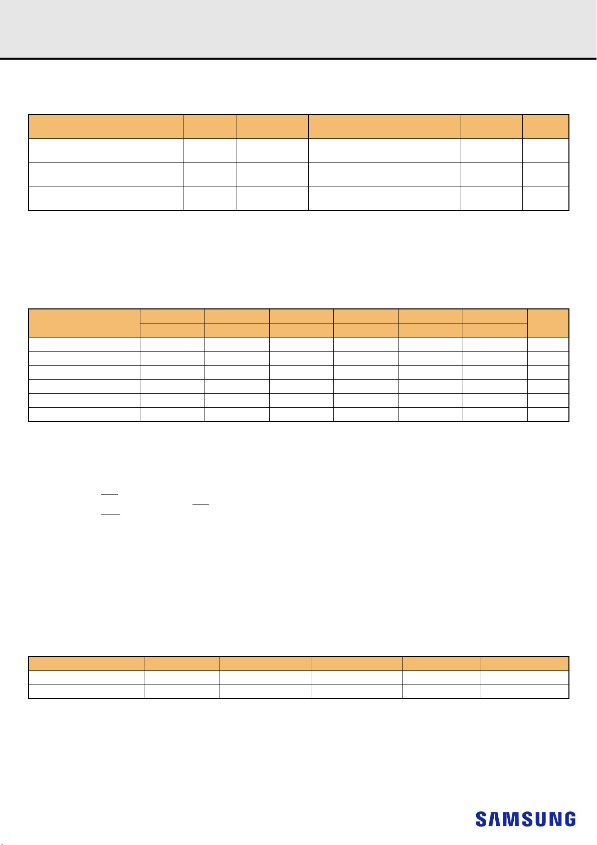
1. DDR4 REGISTERED DIMM ORDERING INFORMATION
[Table 1] Ordering Information Table
Part Number
M393A2K43CB1-CRC
M393A2K43CB2-CTD/VF
M393A2K40CB1-CRC
M393A2K40CB2-CTD/VF
M393A4K40CB1-CRC
M393A4K40CB2-CTD/VF
NOTE :
1) "##"- RC/TD/VF.
2) RC(2400Mbps 17-17-17)/TD(2666Mbps 19-19-19)/VF(2933Mbps 21-21-21).
- Backward compatible to lower frequency.
2)
Density Organization
16GB 2Gx72 1Gx8(K4A8G085WC-BC##)*18 2 31.25mm
16GB 2Gx72 2Gx4(K4A8G045WC-BC##)*18 1 31.25mm
32GB 4Gx72 2Gx4(K4A8G045WC-BC##)*36 2 31.25mm
Component Composition
1)
Number of
Rank
2. KEY FEATURES
[Table 2] Speed Bins
Speed
tCK 1.25 1.071 0.937 0.833 0.75 0.682 ns
CAS Latency 11 13 15 17 19 21 nCK
tRCD 13.75 13.92 14.06 14.16 14.25 14.32 ns
tRP 13.75 13.92 14.06 14.16 14.25 14.32 ns
tRAS 35 34 33 32 32 32 ns
tRC 48.75 47.92 47.06 46.16 46.25 46.32 ns
DDR4-1600 DDR4-1866 DDR4-2133 DDR4-2400 DDR4-2666 DDR4-2933
11-11- 11 13-13-13 15-15-15 17-17-17 19-19-19 21-21-21
Height
Unit
• JEDEC standard 1.2V ± 0.06V Power Supply
•V
• 800 MHz fCK for 1600Mb/sec/pin,933 MHz fCK for 1866Mb/sec/pin, 1067MHz fCK for 2133Mb/sec/pin,1200MHz fCK for 2400Mb/sec/pin, 1333MHz
• 16 Banks (4 Bank Groups)
• Programmable CAS Latency: 10,11,12,13,14,15,16,17,18,19,20,21,22
• Programmable Additive Latency (Posted CAS): 0, CL - 2, or CL - 1 clock
• Programmable CAS Write Latency (CWL) = 9,11 (DDR4-1600), 10,12 (DDR4-1866), 11,14 (DDR4-2133), 12,16 (DDR4-2400), 14,18 (DDR4-2666)
• Burst Length: 8 , 4 with tCCD = 4 which does not allow seamless read or write [either On the fly using A12 or MRS]
• Bi-directional Differential Data Strobe
• On Die Termination using ODT pin
• Average Refresh Period 7.8us at lower then T
• Asynchronous Reset
= 1.2V ± 0.06V
DDQ
for 2666Mb/sec/pin and 1467MHz fCK for 2933Mb/sec/pin.
f
CK
and 16, 20 (DDR4-2933)
85C, 3.9us at 85C < T
CASE
CASE
95C
3. ADDRESS CONFIGURATION
Organization Row Address Column Address Bank Group Address Bank Address Auto Precharge
1Gx8(8Gb) based Module A0-A15 A0-A9 BG0-BG1 BA0-BA1 A10/AP
2Gx4(8Gb) based Module A0-A16 A0-A9 BG0-BG1 BA0-BA1 A10/AP
- 5 -
Rev. 1.5
Registered DIMM
datasheet
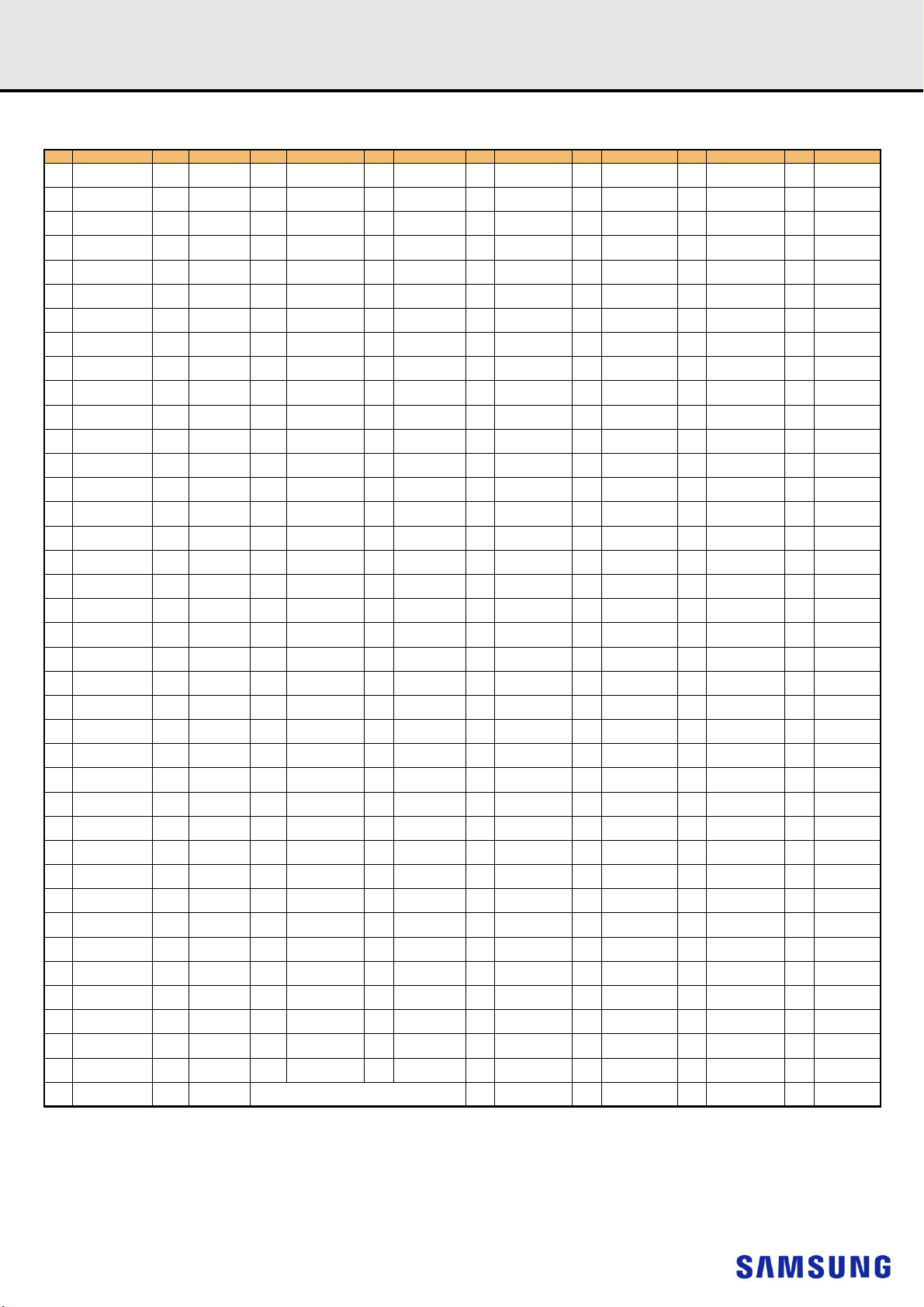
4. REGISTERED DIMM PIN CONFIGURATIONS
DDR4 SDRAM
(FRONT SIDE/BACK SIDE)
Pin Front Pin Back Pin Front Pin Back Pin Front Pin Back Pin Front Pin Back
12V
3
,NC
145
12V3,NC
1
2 VSS 146 VREFCA 41
3 DQ4 147 VSS 42 VSS 186 DQS3
4 VSS 148 DQ5 43 DQ30 187 VSS 81 BA0 225 A10/AP 120 VSS 264 DQ49
5 DQ0 149 VSS 44 VSS 188 DQ31 82 RAS
6 VSS 150 DQ1 45 DQ26 189 VSS 83 VDD 227 RFU 122
TDQS9_t,
7
DQS9_t
TDQS9_c,
8
DQS9_c
9 VSS 153 DQS0
151 VSS 46 VSS 190 DQ27 84 S0
152 DQS0
_c
_t
10 DQ6 154 VSS 49 CB0 193 VSS 87 ODT0 231 VDD 126 DQ50 270 VSS
11 VSS 155 DQ7 50 VSS 194 CB1 88 VDD 232 A13 127 VSS 271 DQ51
12 DQ2 156 VSS 51
13 VSS 157 DQ3 52
14 DQ12 158 VSS 53 VSS 197 DQS8
15 VSS 159 DQ13 54 CB6 198 VSS 92 VDD 236 VDD 131 VSS 275 DQ57
16 DQ8 160 VSS 55 VSS 199 CB7 93 C0,CS2
17 VSS 161 DQ9 56 CB2 200 VSS 94 VSS 238 SA2 133
TDQS10_t,
18
DQS10_t
TDQS10_c,
19
DQS10_c
20 VSS 164 DQS1
162 VSS 57 VSS 201 CB3 95 DQ36 239 VSS 134 VSS 278 DQS7
163 DQS1
_c
_t
21 DQ14 165 VSS 60 CKE0 204 VDD 98 VSS 242 DQ33 137 DQ58 281 VSS
22 VSS 166 DQ15 61 VDD 205 RFU 99
23 DQ10 167 VSS 62 ACT
24 VSS 168 DQ11 63 BG0 207 BG1 101 VSS 245 DQS4
25 DQ20 169 VSS 64 VDD 208 ALERT
26 VSS 170 DQ21 65 A12/BC
27 DQ16 171 VSS 66 A9 210 A11 104 DQ34 248 VSS 143 VPP 287 VPP
28 VSS 172 DQ17 67 VDD 211 A7 105 VSS 249 DQ35 144 RFU 288
TDQS11_t,
29
DQS11_t
TDQS11_c,
30
DQS11_c
31 VSS 175 DQS2
173 VSS 68 A8 212 VDD 106 DQ44 250 VSS
174 DQS2
_c
_t
32 DQ22 176 VSS 71 A3 215 VDD 109 VSS 253 DQ41
33 VSS 177 DQ23 72 A1 216 A2 110
34 DQ18 178 VSS 73 VDD 217 VDD 111
35 VSS 179 DQ19 74 CK0
36 DQ28 180 VSS 75 CK0
37 VSS 181 DQ29 76 VDD 220 VDD 114 VSS 258 DQ47
38 DQ24 182 VSS 77 VTT 221 VTT 115 DQ42 259 VSS
39 VSS 183 DQ25 KEY 116 VSS 260 DQ43
TDQS12_t,
40
DQS12_t
TDQS12_c,
DQS12_c
184 VSS 78 EVENT
185 DQS3
_c
79 A0 223 VDD 118 VSS 262 DQ53
_t
80 VDD 224 BA1 119 DQ48 263 VSS
_n
_n
222 PARITY 117 DQ52 261 VSS
/A16 226 VDD 121
_n
228 WE_n/A14 123 VSS 267 DQS6
TDQS15_t,
DQS15_t
TDQS15_c,
DQS15_c
265 VSS
266 DQS6
47 CB4 191 VSS 85 VDD 229 VDD 124 DQ54 268 VSS
48 VSS 192 CB5 86 CAS_n/A15 230 NC 125 VSS 269 DQ55
TDQS17_t,
DQS17_t
TDQS17_c,
DQS17_c
58 RESET
195 VSS 89 S1
196 DQS8
_n
202 VSS 96 VSS 240 DQ37 135 DQ62 279 VSS
_c
90 VDD 234 A17 129 VSS 273 DQ61
_t
91 ODT1 235 NC,C2 130 DQ56 274 VSS
_n
233 VDD 128 DQ60 272 VSS
_n
,NC 237 NC,CS3_c,C1 132
TDQS16_t,
DQS16_t
TDQS16_c,
DQS16_c
276 VSS
277 DQS7
59 VDD 203 CKE1 97 DQ32 241 VSS 136 VSS 280 DQ63
TDQS13_t,
DQS13_t
_n
206 VDD 100
_n
_n
209 VDD 103 VSS 247 DQ39 142 VPP 286 VPP
TDQS13_c,
DQS13_c
102 DQ38 246 VSS 141 SCL 285 SDA
243 VSS 138 VSS 282 DQ59
244 DQS4
_c
139 SA0 283 VSS
_t
140 SA1 284 VDDSPD
VPP
69 A6 213 A5 107 VSS 251 DQ45
70 VDD 214 A4 108 DQ40 252 VSS
_t
_c
218 CK1
219 CK1
TDQS14_t,
DQS14_t
TDQS14_c,
DQS14_c
_t
112 VS S 25 6 D QS5
_c
113 DQ4 6 2 57 VS S
254 VSS
255 DQS5
_c
_t
_c
_t
_c
_t
4
NOTE :
1) VPP is 2.5V DC.
2) Pin 230 is defined as NC for UDIMMs, RDIMMs and LRDIMMs. Pin 230 is defined as SAVE_n for NVDIMMs.
3) Pins 1 and 145 are defined as NC for UDIMMs, RDIMMs and LRDIMMs. Pins 1 and 145 are defined as 12V for Hybrid /NVDIMM
4) The 5th VPP is required on all modules. DIMMs.
- 6 -
Rev. 1.5
Registered DIMM
datasheet
DDR4 SDRAM
5. PIN DESCRIPOTION
Pin Name Description Pin Name Description
1)
A0–A17
BA0, BA1 Register bank select input SDA I
BG0, BG1 Register bank group select input SA0–SA2 I
RAS_n
CAS_n
WE_n
CS0_n, CS1_n,
CS2_n, CS3_n
CKE0, CKE1 Register clock enable lines input VSS Power supply return (ground)
ODT0, ODT1 Register on-die termination control lines input VDDSPD Serial SPD/TS positive power supply
ACT_n Register input for activate input ALERT_n Register ALERT_n output
DQ0–DQ63 DIMM memory data bus RESET_n Set Register and SDRAMs to a Known State
CB0–CB7 DIMM ECC check bits EVENT_n SPD signals a thermal event has occurred
DQS0_t–
DQS17_t
DQS0_c–
DQS17_c
CK0_t, CK1_t
CK0_c, CK1_c
Register address input SCL I2C serial bus clock for SPD/TS and register
2
C serial bus data line for SPD/TS and register
2
C slave address select for SPD/TS and register
2)
Register row address strobe input PAR Register parity input
3)
Register column address strobe input VDD SDRAM core power supply
4)
Register write enable input VPP SDRAM activating power supply
DIMM Rank Select Lines input VREFCA SDRAM command/address reference supply
Data Buffer data strobes
(positive line of differential pair)
Data Buffer data strobes
(negative line of differential pair)
Register clock input (positive line of differential pair)
Register clocks input (negative line of differential
pair)
VTT
RFU Reserved for future use
SDRAM I/O termination supply
NOTE :
1) Address A17 is only valid for 16Gb x4 based SDRAMs.
2) RAS_n is a multiplexed function with A16.
3) CAS_n is a multiplexed function with A15.
4) WE_n is a multiplexed function with A14.
- 7 -
Rev. 1.5
Thermal sensor
SA0 SA1 SA2
SCL
1K
EVENT_nEVENT_n
SCL
SDASDA
Serial PD with
SA0 SA1 SA2
VSSZQCAL
SCL
SDA
Register
SA0
SA1
SA2
Registered DIMM
datasheet
6. ON DIMM THERMAL SENSOR
NOTE :
1) All Samsung RDIMM support Thermal sensor on DIMM.
[Table 3] Temperature Sensor Characteristics
Grade Range
75 < Ta < 95 - +/- 0.5 +/- 1.0
B
40 < Ta < 125 - +/- 1.0 +/- 2.0 -
-20 < Ta < 125 - +/- 2.0 +/- 3.0 -
Resolution 0.25 C /LSB -
Min. Typ . Max.
Temperature Sensor Accuracy
DDR4 SDRAM
Units NOTE
-
C
- 8 -
Rev. 1.5
Registered DIMM
datasheet
7. INPUT/OUTPUT FUNCTIONAL DESCRIPTION
[Table 4] Input/Output Function Description
Symbol Ty pe Function
CK_t, CK_c
CKE, (CKE1) Input
CS_n, (CS1_n)
C0, C1, C2 Input
ODT, (ODT1) Input
ACT_n Input
RAS_n/A16.
CAS_n/A15.
WE_n/A14
DM_n/DBI_n/
TDQS_t, (DMU_n/
DBIU_n), (DML_n/
DBIL_n)
BG0 - BG1 Input
BA0 - BA1 Input
A0 - A17 Input
A10 / AP Input
A12 / BC_n Input
RESET_n Input
DQ
Input/Output
Input
Input
Input
Input/
Output
Clock: CK_t and CK_c are differential clock inputs. All address and control input signals are sampled on the crossing
of the positive edge of CK_t and negative edge of CK_c.
Clock Enable: CKE HIGH activates and CKE LOW deactivates internal clock signals and device input buffers and
output drivers. Taking CKE LOW provides Precharge Power-Down and Self-Refresh operation (all banks idle), or
Active Power-Down (row Active in any bank). CKE is synchronous for Self-Refresh exit. After VREFCA and Internal
DQ Vref have become stable during the power on and initialization sequence, they must be maintained during all
operations (including Self-Refresh). CKE must be maintained high throughout read and write accesses. Input buffers,
excluding CK_t, CK_c, ODT and CKE, are disabled during power-down. Input buffers, excluding CKE are disabled
during Self-Refresh.
Chip Select: All commands are masked when CS_n is registered HIGH. CS_n provides for external Rank selection on
systems with multiple Ranks. CS_n is considered part of the command code.
Chip ID : Chip ID is only used for 3DS for 2,4,8 high stack via TSV to select each slice of stacked component. Chip ID
is considered part of the command code.
On Die Termination: ODT (registered HIGH) enables RTT_NOM termination resistance internal to the DDR4 SDRAM.
When enabled, ODT is only applied to each DQ, DQS_t, DQS_c and DM_n/DBI_n/ TDQS_t, NU/TDQS_c (When
TDQS is enabled via Mode Register A11=1 in MR1) signal for x8 configurations. For x16 configuration ODT is applied
to each DQ, DQSU_t, DQSU_c, DQSL_t, DQSL_c, DMU_n, and DML_n signal. The ODT pin will be ignored if MR1 is
programmed to disable RTT_NOM.
Activation Command Input : ACT_n defines the Activation command being entered along with CS_n. The input into
RAS_n/A16, CAS_n/A15 and WE_n/A14 will be considered as Row Address A16, A15 and A14
Command Inputs: RAS_n/A16, CAS_n/A15 and WE_n/A14 (along with CS_n) define the command being entered.
Those pins have multi function. For example, for activation with ACT_n Low, these are Addressing like A16, A15 and
A14 but for non-activation command with ACT_n High, these are Command pins for Read, Write and other command
defined in command truth table
Input Data Mask and Data Bus Inversion: DM_n is an input mask signal for write data. Input data is masked when
DM_n is sampled LOW coincident with that input data during a Write access. DM_n is sampled on both edges of
DQS. DM is muxed with DBI function by Mode Register A10,A11,A12 setting in MR5. For x8 device, the function of
DM or TDQS is enabled by Mode Register A11 setting in MR1. DBI_n is an input/output identifing whether to store/
output the true or inverted data. If DBI_n is LOW, the data will be stored/output after inversion inside the DDR4
SDRAM and not inverted if DBI_n is HIGH. TDQS is only supported in X8
Bank Group Inputs: BG0 - BG1 define to which bank group an Active, Read, Write or Precharge command is being
applied. BG0 also determines which mode register is to be accessed during a MRS cycle. X4/8 have BG0 and BG1
but X16 has only BG0.
Bank Address Inputs: BA0 - BA1 define to which bank an Active, Read, Write or Precharge command is being applied.
Bank address also determines which mode register is to be accessed during a MRS cycle.
Address Inputs: Provide the row address for ACTIVATE Commands and the column address for Read/Write
commands to select one location out of the memory array in the respective bank. A10/AP, A12/BC_n, RAS_n/A16,
CAS_n/A15 and WE_n/A14 have additional functions. See other rows. The address inputs also provide the op-code
during Mode Register Set commands. A17 is only defined for the x4 configurations.
Auto-precharge: A10 is sampled during Read/Write commands to determine whether Autoprecharge should be
performed to the accessed bank after the Read/Write operation. (HIGH: Autoprecharge; LOW: no Autoprecharge).
A10 is sampled during a Precharge command to determine whether the Precharge applies to one bank (A10 LOW) or
all banks (A10 HIGH). If only one bank is to be precharged, the bank is selected by bank addresses.
Burst Chop: A12/BC_n is sampled during Read and Write commands to determine if burst chop (on-the-fly) will be
performed. (HIGH, no burst chop; LOW: burst chopped). See command truth table for details.
Active Low Asynchronous Reset: Reset is active when RESET_n is LOW, and inactive when RESET_n is HIGH.
RESET_n must be HIGH during normal operation. RESET_n is a CMOS rail to rail signal with DC high and low at 80%
and 20% of VDD.
Data Input/ Output: Bi-directional data bus. If CRC is enabled via Mode register then CRC code is added at the end of
Data Burst. Any DQ from DQ0-DQ3 may indicate the internal Vref level during test via Mode Register Setting MR4
A4=High. During this mode, RTT value should be set to Hi-Z. Refer to vendor specific datasheets to determine which
DQ is used.
DDR4 SDRAM
- 9 -
Rev. 1.5
Registered DIMM
[Table 4] Input/Output Function Description
Symbol Ty pe Function
Data Strobe: output with read data, input with write data. Edge-aligned with read data, centered in write data. For the
DQS_t, DQS_c,
DQSU_t, DQSU_c,
DQSL_t, DQSL_c
TDQS_t, TDQS_c Output
PAR Input
ALERT_n
TEN
NC No Connect: No internal electrical connection is present.
VDDQ Supply DQ Power Supply: 1.2 V +/- 0.06 V
VSSQ Supply DQ Ground
VDD Supply
VSS Supply
VPP Supply
VREFCA Supply
ZQ Supply
Input/
Output
Input/
Output
Input
x16, DQSL corresponds to the data on DQL0-DQL7; DQSU corresponds to the data on DQU0-DQU7. The data strobe
DQS_t , DQSL_t and DQSU_t are paired with differential signals DQS_c, DQSL_c, and DQSU_c, respectively, to
provide differential pair signaling to the system during reads and writes. DDR4 SDRAM supports differential data
strobe only and does not support single-ended.
Termination Data Strobe: TDQS_t/TDQS_c is applicable for x8 DRAMs only. When enabled via Mode Register A11 =
1 in MR1, the DRAM will enable the same termination resistance function on TDQS_t/TDQS_c that is applied to
DQS_t/DQS_c. When disabled via mode register A11 = 0 in MR1, DM/DBI/TDQS will provide the data mask function
or Data Bus Inversion depending on MR5; A11,12,10and TDQS_c is not used. x4/x16 DRAMs must disable the TDQS
function via mode register A11 = 0 in MR1.
Command and Address Parity Input: DDR4 Supports Even Parity check in DRAM with MR setting. Once it’s enabled
via Register in MR5, then DRAM calculates Parity with ACT_n, RAS_n/A16, CAS_n/A15, WE_n/A14, BG0-BG1, BA0BA1, A17-A0 and C0-C2 (3DS devices). Command and address inputs shall have parity check performed when
commands are latched via the rising edge of CK_t and when CS_n is low.
Alert : It has multi functions such as CRC error flag, Command and Address Parity error flag as Output signal. If there
is error in CRC, then ALERT_n goes LOW for the period time interval and goes back HIGH. If there is error in
Command Address Parity Check, then ALERT_n goes LOW for relatively long period until on going DRAM internal
recovery transaction is complete. During Connectivity Test mode, this pin works as input.
Using this signal or not is dependent on system. In case of not connected as Signal, ALERT_n Pin must be bounded
to VDD on board.
Connectivity Test Mode Enable : Required on X16 devices and optional input on x4/x8 with densities equal to or
greater than 8Gb.HIGH in this pin will enable Connectivity Test Mode operation along with other pins. It is a CMOS rail
to rail signal with AC high and low at 80% and 20% of VDD. Using this signal or not is dependent on System. This pin
may be DRAM internally pulled low through a weak pull-down resistor to VSS.
Power Supply: 1.2 V ± 0.06 V
Ground
DRAM Activating Power Supply: 2.5V (2.375V min, 2.75V max)
Reference voltage for CA
Reference Pin for ZQ calibration.
datasheet
DDR4 SDRAM
NOTE :
1) Input only pins (BG0-BG1,BA0-BA1, A0-A17, ACT_n, RAS_n/A16, CAS_n/A15, WE_n/A14, CS_n, CKE, ODT, and RESET_n) do not supply termination.
- 10 -
Rev. 1.5
Registered DIMM
datasheet
DDR4 SDRAM
8. REGISTERING CLOCK DRIVER SPECIFICATION
8.1 Timing & Capacitance Values
Symbol Parameter Conditions
fclock Input Clock Frequency application frequency 625 1080 625 1350 625 1350 MHz
t
CH/tCL
t
t
PDM
t
C
C
NOTE :
1) This parameter does not include package capacitance.
2) Data inputs are DCKE0/1, DODT0/1, DA0..DA17, DBA0..DBA1, DBG0..DBG1, DACT_n, DC0..DC2, DPAR, DCS0/1_n.
Pulse duration, CK_t, CK_c
HIGH or LOW
Inputs active time4 before
ACT
DRST_n is taken HIGH
Propagation delay, single-bit
switching, CK_t/ CK_c to output
output disable time
DIS
t
output enable time
EN
C
Input capacitance, Data inputs
I
Input capacitance, CK_t, CK_c
CK
Input capacitance, DRST_n
IR
DCKE0/1 = LOW and
DCS0/1_n = HIGH
1.2V Operation 1 1.3 1 1.3 1 1.3 ns
Rising edge of Yn_t to
output float
Output valid to rising
edge of Yn_t
1),2)
NOTE
1),2)
NOTE
or VSS;
V
I=VDD
=1.2V
V
DD
DDR4-1600/1866/2133 DDR4-2400/2666 DDR4-2933
Min Max Min Max Min Max
0.4 - 0.4 - 0.4 -
16 - 16 - 16 -
0.5*tCK +
tQSK1(min)
0.5*tCK -
tQSK1(max)
0.8 1.1 0.8 1.0 0.8 1.0
0.8 1.1 0.8 1.0 0.8 1.0
0.5 2.0 0.5 2.0 0.5 2.0
-
-
0.5*tCK +
tQSK1(min)
0.5*tCK -
tQSK1(max)
-
-
0.5*tCK +
tQSK1(min)
0.5*tCK -
tQSK1(max)
-ps
-ps
Units
t
CK
t
CK
pF
8.2 Clock Driver Characteristics
Symbol Parameter Conditions
t
jit
t
STAB
t
t
jit
t
(hper)
jit
t
t
dynoff
(cc)
CKsk
(per)
Qsk1
Cycle-to-cycle period jitter CK_t/CK_c stable 0
Stabilization time - 5 - 5 - 5 - 5 us
Clock Output skew - 10 - 10 - 10 - 10 ps
Yn Clock Period jitter
Half period jitter
Qn Output to clock toler-
ance
Maximum re-driven
dynamic clock off-set
DDR4-1600/1866/
2133
Min Max Min Max Min Max Min Max
0.025 x
tCK
-0.025 *
tCK
-0.032 *
tCK
-0.125 *
tCK
0.025 *
tCK
0.032 *
tCK
0.125 *
tCK
- 50 - 45 - 45 - 40 ps
DDR4-2400 DDR4-2666 DDR4-2933
0
-0.025 *
tCK
-0.032 *
tCK
-0.125 *
tCK
0.025 x
tCK
0.025 *
tCK
0.032 *
tCK
0.125 *
tCK
-0.025 *
tCK
-0.032 *
tCK
-0.1 * tCK 0.1 * tCK -0.1 * tCK 0.1 * tCK ps
0.025 x
0
tCK
0.025 *
tCK
0.032 *
tCK
0
-0.025 *
tCK
-0.032 *
tCK
0.025 x
tCK
0.025 *
tCK
0.032 *
tCK
Units
ps
ps
ps
- 11 -
Rev. 1.5
DQS8_t
DQS8_c
CB[7:0]
DQS_t
DQS_c
U5
CKE
ODT
ZQ
DQ[7:0]
CS_n
ODT0A
CS0A_n
VSS
DBI8_n/DM8_n DBI_n/DM_n
DQS3_t
DQS3_c
DQ[31:24]
DQS_t
DQS_c
U4
CKE
ODT
ZQ
DQ[7:0]
CS_n
VSS
DBI3_n/DM3_n DBI_n/DM_n
DQS2_t
DQS2_c
DQ[23:16]
DQS_t
DQS_c
U3
CKE
ODT
ZQ
DQ[7:0]
CS_n
VSS
DBI2_n/DM2_n DBI_n/DM_n
DQS1_t
DQS1_c
DQ[15:8]
DQS_t
DQS_c
U2
CKE
ODT
ZQ
DQ[7:0]
CS_n
VSS
DBI1_n/DM1_n DBI_n/DM_n
DQS0_t
DQS0_c
DQ[7:0]
DQS_t
DQS_c
U1
CKE
ODT
ZQ
DQ[7:0]
CS_n
VSS
DBI0_n/DM0_n DBI_n/DM_n
DQS_t
DQS_c
U14
CKE
ODT
ZQ
DQ[7:0]
CS_n
VSS
DBI_n/DM_n
DQS_t
DQS_c
U13
CKE
ODT
ZQ
DQ[7:0]
CS_n
VSS
DBI_n/DM_n
DQS_t
DQS_c
U12
CKE
ODT
ZQ
DQ[7:0]
CS_n
VSS
DBI_n/DM_n
DQS_t
DQS_c
U11
CKE
ODT
ZQ
DQ[7:0]
CS_n
VSS
DBI_n/DM_n
DQS_t
DQS_c
U10
CKE
ODT
ZQ
DQ[7:0]
CS_n
VSS
DBI_n/DM_n
CS1A_n
ODT1A
CKE1A
DQS4_t
DQS4_c
DQ[39:32]
DQS_t
DQS_c
U6
CKE
ODT
ZQ
DQ[7:0]
CS_n
CS1B_n
ODT1B
CKE1B
VSS
DBI4_n/DM4_n DBI_n/DM_n
DQS5_t
DQS5_c
DQ[47:40]
DQS_t
DQS_c
U7
CKE
ODT
ZQ
DQ[7:0]
CS_n
VSS
DBI5_n/DM5_n DBI_n/DM_n
DQS6_t
DQS6_c
DQ[55:48]
DQS_t
DQS_c
U8
CKE
ODT
ZQ
DQ[7:0]
CS_n
VSS
DBI6_n/DM6_n DBI_n/DM_n
DQS7_t
DQS7_c
DQ[63:56]
DQS_t
DQS_c
U9
CKE
ODT
ZQ
DQ[7:0]
CS_n
VSS
DBI7_n/DM7_n DBI_n/DM_n
DQS_t
DQS_c
U15
CKE
ODT
ZQ
DQ[7:0]
CS_n
VSS
DBI_n/DM_n
DQS_t
DQS_c
U16
CKE
ODT
ZQ
DQ[7:0]
CS_n
VSS
DBI_n/DM_n
DQS_t
DQS_c
U17
CKE
ODT
ZQ
DQ[7:0]
CS_n
VSS
DBI_n/DM_n
DQS_t
DQS_c
U18
CKE
ODT
ZQ
DQ[7:0]
CS_n
VSS
DBI_n/DM_n
CS0B_n
ODT0B
CKE0B
CKE0A
Registered DIMM
datasheet
DDR4 SDRAM
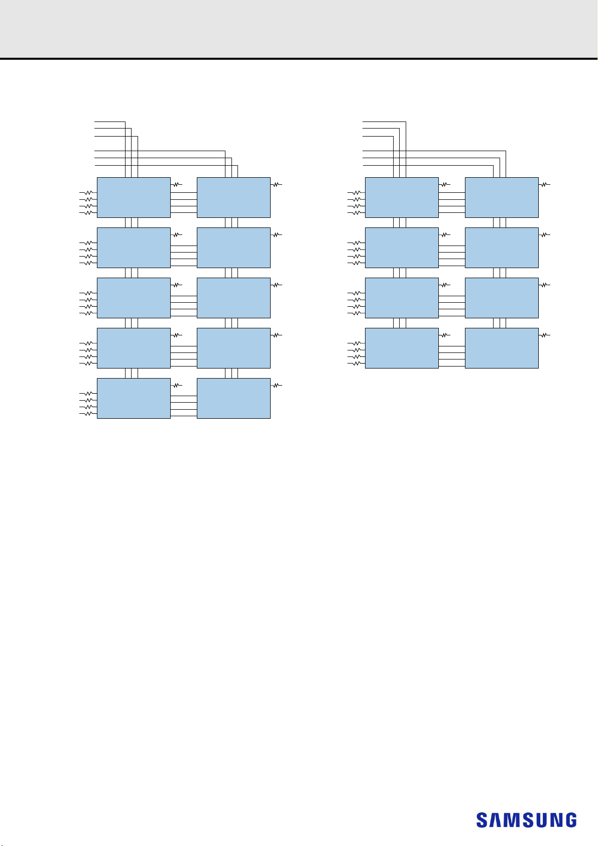
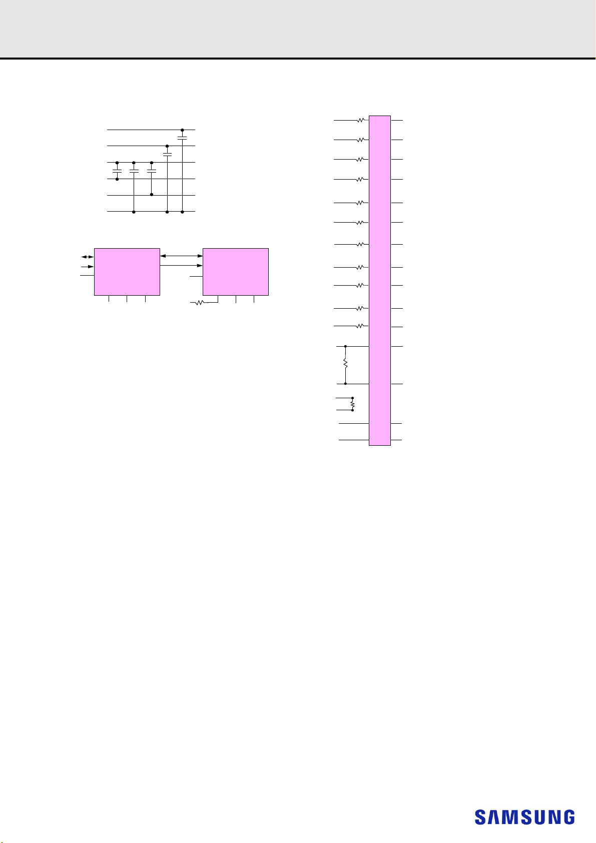
9. FUNCTION BLOCK DIAGRAM:
9.1 16GB, 2Gx72 Module (Populated as 2 rank of x8 DDR4 SDRAMs)
NOTE :
1) Unless otherwise noted, resistor values are 15 5%.
2) See the Net Structure diagrams for all resistors associated with the command, address and control bus.
3) ZQ resistors are 240 1%. For all other resistor values refer to the appropriate wiring diagram.
4) VDDSPD connects to the RCD and the SPD-TSE.
- 12 -
Rev. 1.5
R
E
G
I
S
T
E
R
BA[1:0]
A[17:0]
ACT_n
PARITY
CKE0
RESET_n
BA[1:0]A -> BA[1:0]: SDRAMs U[5:1], U[14:10]
A[16:0]A -> A[16:0]: SDRAMs U[5:1], U[14:10]
ACTA_n -> ACT_n: SDRAMs U[5:1], U[14:10]
CKE0A -> CKE: SDRAMs U[5:1]
BG[1:0] BG[1:0]A -> BG[1:0] : SDRAMs
U[5:1], U[14:10]
BA[1:0]B -> BA[1:0]: SDRAMs U[9:6], U[18:15]
A[16:0]B -> A[16:0]: SDRAMs U[9:6], U[18:15]
ACTB_n -> ACT_n: SDRAMs U[9:6], U[18:15]
PARA -> PAR: SDRAMs U[5:1], U[14:10]
PARB -> PAR: SDRAMs U[9:6], U[18:15]
CKE0B -> CKE: SDRAMs U[9:6]
Y0_c -> CK_c: SDRAMs U[9:6]
Y1_c -> CK_c: SDRAMs U[5:1]
QRST_n -> RESET_n: All SDRAM
CK0_c
ODT0
CK0_t
Y0_t -> CK_t: SDRAMs U[9:6]
Y1_t -> CK_t: SDRAMs U[5:1]
BG[1:0]B-> BG[1:0]: SDRAMs U[9:6], U[18:15]
CK1_c
CK1
_t
CS0_n
ALERT_n
ERROR_IN_n <- ALERT_n: All SDRAMs
ODT0A -> ODT: SDRAMs U[5:1]
ODT0B -> ODT: SDRAMs U[9:6]
CS0A_n -> CS_n: SDRAMs U[5:1]
CS0B_n -> CS_n: SDRAMs U[9:6]
V
SS
V
PP
U1 - U18
V
TT
V
DDSPD
Serial PD
V
DD
V
REFCA
SA0 SA1 SA2
SCL
EVENT_n EVENT_n
SCL
SDASDA
Serial PD with Thermal sensor
SA0 SA1 SA2
VSS
BFUNC
SCL
SDA
U1 - U18
U1 - U18
U1 - U18
SA0 SA1 SA2
SA1
SA2
SA0
1K
5%
RCD
CKE1A -> CKE: SDRAMs U[14:10]
CKE1B -> CKE: SDRAMs U[18:15]
ODT1A -> ODT: SDRAMs U[14:10
ODT1B -> ODT: SDRAMs U[18:15]
CS1A_n -> CS_n: SDRAMs U[14;10]
CS1B_n -> CS_n: SDRAMs U[18:15]
Y2_t -> CK_t: SDRAMs U[18:15]
Y3_t -> CK_t: SDRAMs U[14:10]
Y2_c -> CK_c: SDRAMs U[18:15]
Y3_c -> CK_c: SDRAMs U[14:10]
CKE1
ODT1
CS1_n
Registered DIMM
datasheet
DDR4 SDRAM
- 13 -
Rev. 1.5
DQS0_t
DQS0_c
DQ[3:0]
DQS_t
DQS_c
D1
CKE
ODT
ZQ
DQ[3:0]
CS_n
DQS1_t
DQS1_c
DQ[11:8]
DQS_t
DQS_c
D2
CKE
ODT
ZQ
DQ[3:0]
CS_n
DQS2_t
DQS2_c
DQ[19:16]
DQS_t
DQS_c
D3
CKE
ODT
ZQ
DQ[3:0]
CS_n
DQS3_t
DQS3_c
DQ[27:24]
DQS_t
DQS_c
D4
CKE
ODT
ZQ
DQ[3:0]
CS_n
DQS8_t
DQS8_c
CB[3:0]
DQS_t
DQS_c
D5
CKE
ODT
ZQ
DQ[3:0]
CS_n
DQS_t
DQS_c
D6
CKE
ODT
ZQ
DQ[3:0]
CS_n
DQS_t
DQS_c
D7
CKE
ODT
ZQ
DQ[3:0]
CS_n
DQS_t
DQS_c
D8
CKE
ODT
ZQ
DQ[3:0]
CS_n
DQS_t
DQS_c
D9
CKE
ODT
ZQ
DQ[3:0]
CS_n
DQS_t
DQS_c
D10
CKE
ODT
ZQ
DQ[3:0]
CS_n
DQS_t
DQS_c
D15
CKE
ODT
ZQ
DQ[3:0]
CS_n
DQS_t
DQS_c
D16
CKE
ODT
ZQ
DQ[3:0]
CS_n
DQS_t
DQS_c
D17
CKE
ODT
ZQ
DQ[3:0]
CS_n
DQS_t
DQS_c
D18
CKE
ODT
ZQ
DQ[3:0]
CS_n
DQS4_t
DQS4_c
DQ[35:32]
DQS_t
DQS_c
D11
CKE
ODT
ZQ
DQ[3:0]
CS_n
DQS5_t
DQS5_c
DQ[43:40]
DQS_t
DQS_c
D12
CKE
ODT
ZQ
DQ[3:0]
CS_n
DQS6_t
DQS6_c
DQ[51:48]
DQS_t
DQS_c
D13
CKE
ODT
ZQ
DQ[3:0]
CS_n
DQS7_t
DQS7_c
DQ[59:56]
DQS_t
DQS_c
D14
CKE
ODT
ZQ
DQ[3:0]
CS_n
QACS0_n
QAODT0
QACKE0
QBCS0_n
QBODT0
QBCKE0
VSS VSS VSSVSSVSS
VSS VSS VSSVSSVSS
VSS VSSVSSVSS
VSS VSSVSSVSS
R
E
G
I
S
T
E
R
BA[1:0]
A[17:0]
ACT_n
PARITY
CKE0
RESET_n
QABA[1:0] -> BA[1:0] : SDRAMs D[10:1]
QAA[17:0] -> A[17:0] : SDRAMs D[10:1]
QAACT_n -> ACT_n : SDRAMs D[10:1]
QACKE0 -> CKE : SDRAMs D[10:1]
BG[1:0] QABG[1:0] -> BG[1:0] : SDRAMs D[10:1]
QBBA[1:0] -> BA[1:0] : SDRAMs D[18:11]
QBA[17:0] -> A[17:0] : SDRAMs D[18:11]
QBACT_n -> ACT_n : SDRAMs D[18:11]
QAPAR -> PAR : SDRAMs D[10:1]
QBPAR -> PAR : SDRAMs D[18:11]
QBCKE0 -> CKE : SDRAMs D[18:11]
Y0_c -> CK_c : SDRAMs D[18:11]
Y1_c -> CK_c : SDRAMs D[10:1]
QRST_n -> RESET_n : All SDRAMs
CK0_c
ODT0
CK0_t
Y0_t -> CK_t : SDRAMs D[18:11]
Y1
_t
-> CK_t : SDRAMs D[10:1]
QBBG[1:0] -> BG[1:0] : SDRAMs D[18:11]
CK1_c
CK1_t
CS0_n
ALERT_n
ERROR_IN_n -> ALERT_n : All SDRAMs
QAODT0 -> ODT : SDRAMs D[10:1]
QBODT0 -> ODT : SDRAMs D[18:11]
QACS0_n -> CS_n : SDRAMs D[10:1]
QBCS0_n -> CS_n : SDRAMs D[18:11]
V
SS
V
PP
D1 - D18
V
TT
V
DDSPD
Serial PD
V
DD
V
REFCA
Thermal sensor
SA0 SA1 SA2
SCL
1K
EVENT_nEVENT_n
SCL
SDASDA
Serial PD with
SA0 SA1 SA2
VSSZQCAL
SCL
SDA
Register
SA0
SA1
SA2
D1 - D18
D1 - D18
D1 - D18
DQS9_t
DQS9_c
DQ[7:4]
DQS10_t
DQS10_c
DQ[15:12]
DQS11_t
DQS11_c
DQ[23:20]
DQS12_t
DQS12_c
DQ[31:28]
DQS17_t
DQS17_c
CB[7:4]
DQS13_t
DQS13_c
DQ[39:36]
DQS14_t
DQS14_c
DQ[47:44]
DQS15_t
DQS15_c
DQ[55:52]
DQS16_t
DQS16_c
DQ[63:60]
Registered DIMM
datasheet
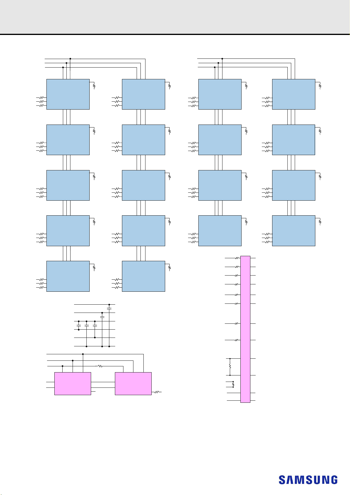
9.2 16GB, 2Gx72 Module (Populated as 1 rank of x4 DDR4 SDRAMs)
DDR4 SDRAM
NOTE :
1) Unless otherwise noted, resistor values are 15 5%.
2) See the Net Structure diagrams for all resistors associated with the command, address and control bus.
3) ZQ resistors are 240 1%. For all other resistor values refer to the appropriate wiring diagram.
- 14 -
Rev. 1.5
DQS0_t
DQS0_c
DQ[3:0]
DQS_t
DQS_c
D6
CKE
ODT
ZQ
DQ[3:0]
CS
_n
DQS1_t
DQS1_c
DQ[11:8]
DQS_t
DQS_c
D7
CKE
ODT
ZQ
DQ[3:0]
CS
_n
DQS2_t
DQS2_c
DQ[19:16]
DQS_t
DQS_c
D8
CKE
ODT
ZQ
DQ[3:0]
CS
_n
DQS3_t
DQS3_c
DQ[27:24]
DQS_t
DQS_c
D9
CKE
ODT
ZQ
DQ[3:0]
CS
_n
DQS_t
DQS_c
D16
CKE
ODT
ZQ
DQ[3:0]
CS
_n
DQS_t
DQS_c
D17
CKE
ODT
ZQ
DQ[3:0]
CS
_n
DQS_t
DQS_c
D18
CKE
ODT
ZQ
DQ[3:0]
CS
_n
DQS_t
DQS_c
D19
CKE
ODT
ZQ
DQ[3:0]
CS
_n
DQS_t
DQS_c
D11
CKE
ODT
ZQ
DQ[3:0]
CS
_n
DQS_t
DQS_c
D12
CKE
ODT
ZQ
DQ[3:0]
CS
_n
DQS_t
DQS_c
D13
CKE
ODT
ZQ
DQ[3:0]
CS
_n
DQS_t
DQS_c
D14
CKE
ODT
ZQ
DQ[3:0]
CS
_n
DQS9_t
DQS9_c
DQ[7:4]
DQS_t
DQS_c
D1
CKE
ODT
ZQ
DQ[3:0]
CS
_n
DQS10_t
DQS10_c
DQ[15:12]
DQS_t
DQS_c
D2
CKE
ODT
ZQ
DQ[3:0]
CS
_n
DQS11_t
DQS11_c
DQ[23:20]
DQS_t
DQS_c
D3
CKE
ODT
ZQ
DQ[3:0]
CS
_n
DQS12_t
DQS12_c
DQ[31:28]
DQS_t
DQS_c
D4
CKE
ODT
ZQ
DQ[3:0]
CS
_n
QACS0
_n
QAODT0
QACKE0
VSS VSSVSSVSS
VSS VSSVSSVSS
VSS VSSVSSVSS
VSS VSSVSSVSS
Thermal sensor
SA0 SA1 SA2
SCL
1K
EVENT_nEVENT_n
SCL
SDASDA
Serial PD with
SA0 SA1 SA2
VSSZQCAL
SCL
SDA
Register
SA0
SA1
SA2
QACS1
_n
QAODT1
QACKE1
DQS8_t
DQS8_c
CB[3:0]
DQS_t
DQS_c
D10
CKE
ODT
ZQ
DQ[3:0]
CS
_n
DQS_t
DQS_c
D20
CKE
ODT
ZQ
DQ[3:0]
CS
_n
DQS_t
DQS_c
D15
CKE
ODT
ZQ
DQ[3:0]
CS
_n
DQS17_t
DQS17_c
CB[7:4]
DQS_t
DQS_c
D5
CKE
ODT
ZQ
DQ[3:0]
CS
_n
VSS
VSS
VSS
VSS
V
SS
V
PP
D1 - D36
V
TT
V
DDSPD
Serial PD
V
DD
V
REFCA
D1 - D36
D1 - D36
D1 - D36
Registered DIMM
datasheet
DDR4 SDRAM
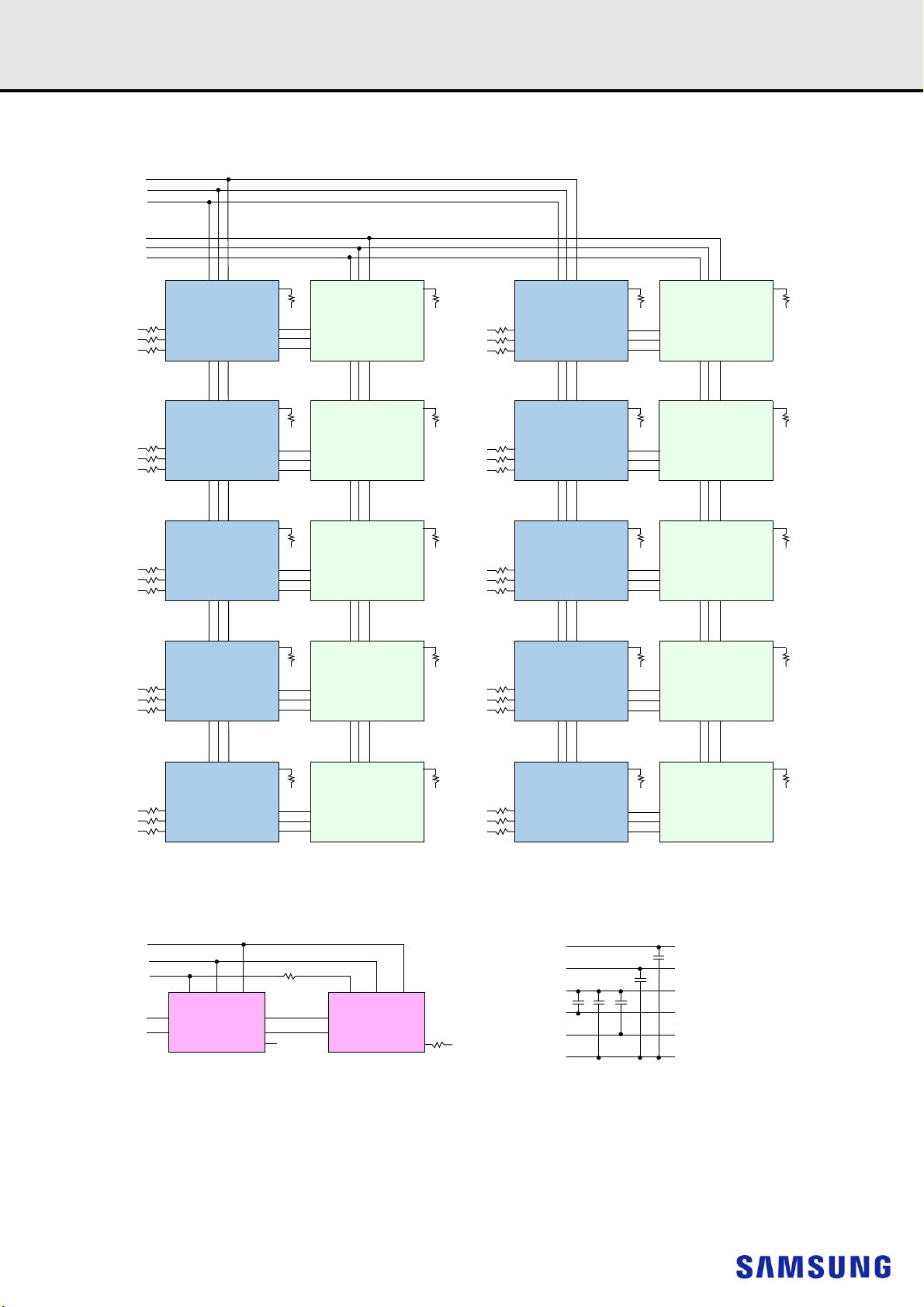
9.3 32GB, 4Gx72 Module (Populated as 2 ranks of x4 DDR4 SDRAMs)
NOTE :
1) Unless otherwise noted, resistor values are 15 5%.
2) See the Net Structure diagrams for all resistors associated with the command, address and control bus.
3) ZQ resistors are 240 1%. For all other resistor values refer to the appropriate wiring diagram.
- 15 -
Rev. 1.5
DQS4_t
DQS4_c
DQ[35:32]
DQS_t
DQS_c
D25
CKE
ODT
ZQ
DQ[3:0]
CS
_n
DQS5_t
DQS5_c
DQ[43:40]
DQS_t
DQS_c
D26
CKE
ODT
ZQ
DQ[3:0]
CS
_n
DQS6_t
DQS6_c
DQ[51:48]
DQS_t
DQS_c
D27
CKE
ODT
ZQ
DQ[3:0]
CS
_n
DQS7_t
DQS7_c
DQ[59:56]
DQS_t
DQS_c
D28
CKE
ODT
ZQ
DQ[3:0]
CS
_n
DQS_t
DQS_c
D33
CKE
ODT
ZQ
DQ[3:0]
CS
_n
DQS_t
DQS_c
D34
CKE
ODT
ZQ
DQ[3:0]
CS
_n
DQS_t
DQS_c
D35
CKE
ODT
ZQ
DQ[3:0]
CS
_n
DQS_t
DQS_c
D36
CKE
ODT
ZQ
DQ[3:0]
CS
_n
DQS_t
DQS_c
D29
CKE
ODT
ZQ
DQ[3:0]
CS
_n
DQS_t
DQS_c
D30
CKE
ODT
ZQ
DQ[3:0]
CS
_n
DQS_t
DQS_c
D31
CKE
ODT
ZQ
DQ[3:0]
CS
_n
DQS_t
DQS_c
D32
CKE
ODT
ZQ
DQ[3:0]
CS
_n
DQS13_t
DQS13_c
DQ[39:36]
DQS_t
DQS_c
D21
CKE
ODT
ZQ
DQ[3:0]
CS
_n
DQS14_t
DQS14_c
DQ[47:44]
DQS_t
DQS_c
D22
CKE
ODT
ZQ
DQ[3:0]
CS
_n
DQS15_t
DQS15_c
DQ[55:52]
DQS_t
DQS_c
D23
CKE
ODT
ZQ
DQ[3:0]
CS
_n
DQS16_t
DQS16_c
DQ[63:60]
DQS_t
DQS_c
D24
CKE
ODT
ZQ
DQ[3:0]
CS
_n
QBCS0_n
QBODT0
QBCKE0
VSS VSSVSSVSS
VSS VSSVSSVSS
VSS VSSVSSVSS
VSS VSSVSSVSS
QBCS1_n
QBODT1
QBCKE1
R
E
G
I
S
T
E
R
BA[1:0]
A[17:0]
ACT
_n
C[2:0]
PARITY
CKE0
CKE1
RESET
_n
QABA[1:0] -> BA[1:0] : SDRAMs D[20:1]
QAA[17:0] -> A[17:0] : SDRAMs D[20:1]
QAACT_n -> ACT_n : SDRAMs D[20:1]
QAC[2:0] -> C[2:0] : SDRAMs D[20:1]
QACKE0 -> CKE : SDRAMs D[10:1]
BG[1:0] QABG[1:0] -> BG[1:0] : SDRAMs D[20:1]
QBBA[1:0] -> BA[1:0] : SDRAMs D[36:21]
QBA[17:0] -> A[17:0] : SDRAMs D[36:21]
QBACT_n -> ACT_n : SDRAMs D[36:21]
QBC[2:0] -> C[2:0] : SDRAMs D[36:21]
QAPAR -> PAR : SDRAMs D[20:1]
QBPAR -> PAR : SDRAMs D[36:21]
QBCKE0 -> CKE : SDRAMs D[28:21]
Y0
_c
-> CK_c : SDRAMs D[24:21], D[32:29]
Y1
_c
-> CK_c: SDRAMs D[5:1], D[15:11]
QRST
_n
-> RESET_n : All SDRAMs
CK0
_c
ODT0
QACKE1 -> CKE : SDRAMs D[20:11]
QBCKE1 -> CKE : SDRAMs D[36:29]
CK0
_t
Y0_t -> CK_t : SDRAMs D[24:21], D[32:29]
Y1
_t
-> CK_t : SDRAMs D[5:1], D[15:11]
QBBG[1:0] -> BG[1:0] : SDRAMs D[36:21]
CK
1
_c
CK1
_t
ODT1
CS0
_n
CS1
_n
ALERT
_n
ERROR_IN_n - ALERT_n : All SDRAMs
QAODT0 -> ODT : SDRAMs D[10:1]
QBODT0 -> ODT : SDRAMs D[28:21]
QAODT1 -> ODT : SDRAMs D[20:11]
QBODT1 -> ODT : SDRAMs D[36:29]
QACS0_n -> CS_n : SDRAMs D[10:1]
QBCS0_n -> CS_n : SDRAMs D[28:21]
QACS1_n -> CS_n : SDRAMs D[20:11]
QBCS1_n -> CS_n : SDRAMs D[36:29]
Y2
_t
-> CK_t : SDRAMs D[28:25], D[36:33]
Y3
_t
-> CK_t : SDRAMs D[10:6], D[20:16]
Y2
_c
-> CK_c : SDRAMs D[28:25], D[36:33]
Y3
_c
-> CK_c : SDRAMs D[10:6], D[20:16]
Registered DIMM
datasheet
DDR4 SDRAM
NOTE :
CK0_t, CK0_c terminated with 120 ± 5% resistor
1)
2) CK1_t, CK1_c terminated with 120 ± 5% resistor but not used.
3) Unless otherwise noted resistors are 22 ± 5%.
.
- 16 -
Rev. 1.5
Registered DIMM
datasheet
DDR4 SDRAM
10. ABSOLUTE MAXIMUM RATINGS
[Table 5] Absolute Maximum DC Ratings
Symbol Parameter Rating Units NOTE
VDD Voltage on VDD pin relative to Vss -0.3 ~ 1.5 V 1,3
VDDQ Voltage on VDDQ pin relative to Vss -0.3 ~ 1.5 V 1,3
VPP Voltage on VPP pin relative to Vss -0.3 ~ 3.0 V 4
V
NOTE :
1) Stresses greater than those listed under “Absolute Maximum Ratings” may cause permanent damage to the device. This is a stress rating only and functional operation of the
device at these or any other conditions above those indicated in the operational sections of this specification is not implied. Exposure to absolute maximum rating conditions
for extended periods may affect reliability
2) Storage Temperature is the case surface temperature on the center/top side of the DRAM. For the measurement conditions, please refer to JESD51-2 standard.
3) VDD and VDDQ must be within 300mV of each other at all times; and VREFCA must be not greater than 0.6 x VDDQ, When VDD and VDDQ are less than 500mV; VREFCA
may be equal to or less than 300mV
4) VPP must be equal or greater than VDD/VDDQ at all times.
5) Overshoot area above 1.5 V is specified in 12.3.4, 12.3.5 and 12.3.6.
Voltage on any pin except VREFCA relative to Vss -0.3 ~ 1.5 V 1,3,5
IN, VOUT
T
Storage Temperature -55 to +100 °C 1,2
STG
11. AC & DC OPERATING CONDITIONS
[Table 6] Recommended DC Operating Conditions
Symbol Parameter
VDD Supply Voltage 1.14 1.2 1.26 V 1,2,3
VDDQ Supply Voltage for Output 1.14 1.2 1.26 V 1,2,3
VPP Peak-to-Peak Voltage 2.375 2.5 2.75 V 3
NOTE
:
1) Under all conditions V
tracks with VDD. AC parameters are measured with VDD and V
2) V
DDQ
3) DC bandwidth is limited to 20MHz.
must be less than or equal to VDD.
DDQ
Min. Typ. Max.
tied together.
DDQ
Rating
Unit NOTE
- 17 -
Rev. 1.5
voltage
V
DD
V
SS
time
Registered DIMM
datasheet
DDR4 SDRAM
12. AC & DC INPUT MEASUREMENT LEVELS
12.1 AC & DC Logic Input Levels for Single-Ended Signals
[Table 7] Single-ended AC & DC Input Levels for Command and Address
Symbol Parameter
VIH.CA(DC75)
VIH.CA(DC65) - -
VIL.CA(DC75)
VIL.CA(DC65) - - VSS
VIH.CA(AC100)
VIH.CA(AC90) - -
VIL.CA(AC100)
VIL.CA(AC90) - - Note 2
VREFCA(DC) Reference Voltage for ADD, CMD inputs 0.49*VDD 0.51*VDD 0.49*VDD 0.51*VDD V 2,3
NOTE
:
1) See “Overshoot and Undershoot Specifications” on section12.3.
2) The AC peak noise on VREFCA may not allow VREFCA to deviate from VREFCA(DC) by more than ± 1% VDD (for reference : approx. ± 12mV)
3) For reference : approx. VDD/2 ± 12mV.
DC input logic high
DC input logic low
AC input logic high
AC input logic low
DDR4-1600/1866/2133/2400 DDR4-2666/2933
Min. Max. Min. Max.
+ 0.075
V
REFCA
V
VSS
+ 0.1
REF
Note 2
VDD - -
V
+ 0.065
REFCA
V
-0.075
REFCA
Note 2 - -
V
- 0.1
REF
--
V
+ 0.09
REF
--
V
REFCA
V
Unit NOTE
VDD
-0.065
Note 2 1
- 0.09
REF
V
V
V
V
1
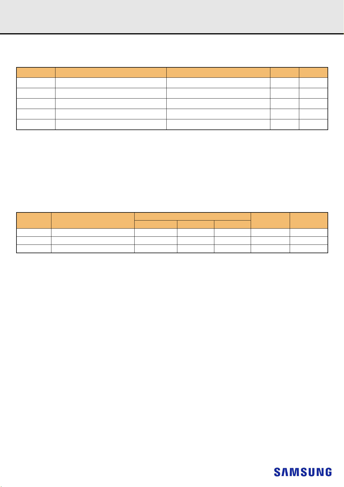
12.2 AC and DC Input Measurement Levels: V
The DC-tolerance limits and ac-noise limits for the reference voltages V
function of time. (V
V
(DC) is the linear average of V
REF
Furthermore V
The voltage levels for setup and hold time measurements VIH(AC), VIH(DC), VIL(AC) and VIL(DC) are dependent on V
stands for V
REF
(t) may temporarily deviate from V
REF
).
REFCA
(t) over a very long period of time (e.g. 1 sec). This average has to meet the min/max requirement in Table 7.
REF
(DC) by no more than ± 1% VDD.
REF
Figure 1. Illustration of V
(DC) tolerance and V
REF
is illustrated in Figure 1. It shows a valid reference voltage V
REFCA
Tolerances.
REF
AC-noise limits
REF
REF
(t) as a
REF
.
"V
" shall be understood as V
REF
This clarifies, that DC-variations of V
which setup and hold is measured. System timing and voltage budgets need to account for V
data-eye of the input signals.
This also clarifies that the DRAM setup/hold specification and derating values need to include time and voltage associated with V
and voltage effects due to AC-noise on V
(DC), as defined in Figure 1.
REF
affect the absolute voltage a signal has to reach to achieve a valid high or low level and therefore the time to
REF
(DC) deviations from the optimum position within the
REF
up to the specified limit (+/-1% of VDD) are included in DRAM timings and their associated deratings.
REF
- 18 -
AC-noise. Timing
REF
Rev. 1.5
0.0
tDVAC
V
IH
.DIFF.MIN
half cycle
Differential Input Voltage (CK-CK)
time
tDVAC
VIH.DIFF.AC.MIN
V
IL
.DIFF.MAX
V
IL
.DIFF.AC.MAX
(CK_t - CK_c)
Registered DIMM
datasheet
12.3 AC and DC Logic Input Levels for Differential Signals
12.3.1 Differential Signals Definition
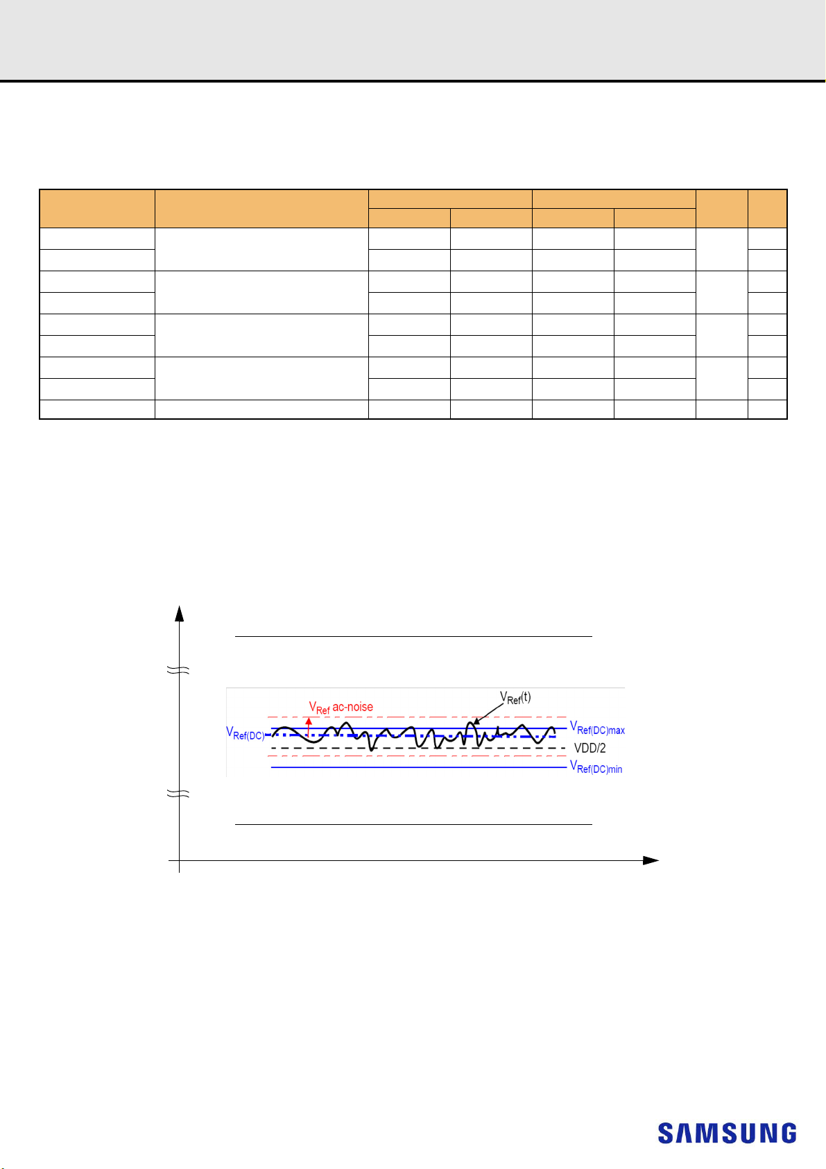
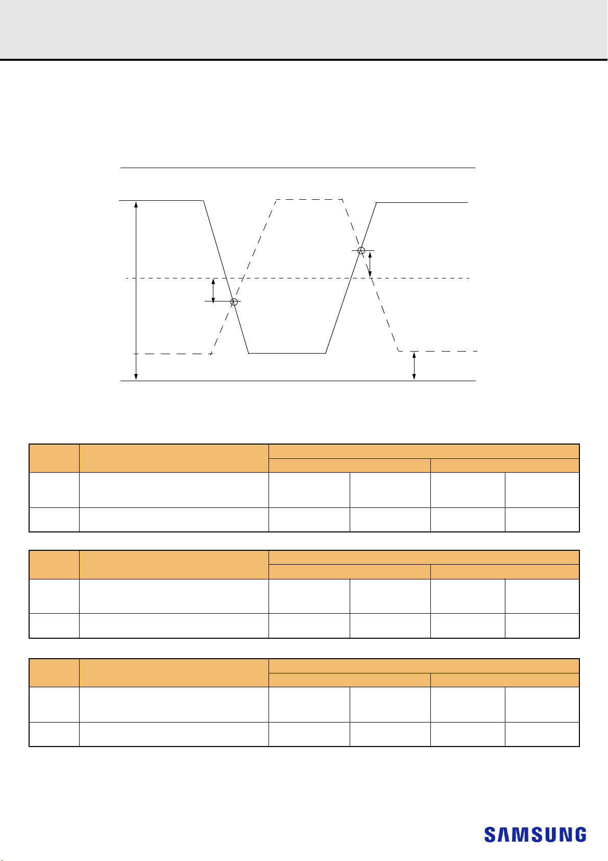
Figure 2. Definition of differential ac-swing and “time above ac-level” t
NOTE
:
1) Differential signal rising edge from VIL.DIFF.MAX to VIH.DIFF.MIN must be monotonic slope.
2) Differential signal falling edge from VIH.DIFF.MIN to VIL.DIFF.MAX must be monotonic slope.
DDR4 SDRAM
DVAC
12.3.2 Differential Swing Requirements for Clock (CK_t - CK_c)
[Table 8] Differential AC and DC Input Levels
Symbol Parameter
V
IHdiff
V
ILdiff
V
IHdiff
V
ILdiff
NOTE :
1) Used to define a differential signal slew-rate.
2) for CK_t - CK_c use V
3) These values are not defined; however, the differential signals CK_t - CK_c, need to be within the respective limits (V
as well as the limitations for overshoot and undershoot.
differential input high 0.150 NOTE 3 0.135 NOTE 3 0.125 NOTE 3 V 1
differential input low NOTE 3 -0.150 NOTE 3 -0.135 NOTE 3 -0.125 V 1
(AC)
differential input high ac
(AC)
differential input low ac NOTE 3
IH.CA/VIL.CA
(AC) of ADD/CMD and V
[Table 9] Allowed Time Before Ringback (tDVAC) for CK_t - CK_c
Slew Rate [V/ns]
> 4.0 120 -
4.0 115 -
3.0 110 -
2.0 105 -
1.8 100 -
1.6 95 -
1.4 90 -
1.2 85 -
1.0 80 -
< 1.0 80 -
DDR4 -1600/1866/2133 DDR4 -2400/2666 DDR4-2933
min max min max min max
2 x (V
V
IH
REF
(AC) -
)
REFCA
NOTE 3
2 x (V
V
;
IL
REF
(AC) -
)
2 x (V
V
NOTE 3
IH
REF
(AC) -
)
2 x (V
tDVAC [ps] @ |V
min max
NOTE 3
(AC) -
IL
V
REF
IH/Ldiff
2 x (V
(DC) max, V
IH.CA
NOTE 3
)
(AC)| = 200mV
V
(AC) -
IH
REF
)
IL.CA
NOTE 3 V 2
(AC) -
2 x (V
IL
V
REF
(DC)min) for single-ended signals
)
NOT
unit
E
V2
- 19 -
Rev. 1.5
VDD or V
DDQ
V
SEH
min
V
DD
/2 or V
DDQ
/2
V
SEL
max
V
SEH
VSS or V
SSQ
V
SEL
CK
time
Registered DIMM
datasheet
DDR4 SDRAM
12.3.3 Single-ended Requirements for Differential Signals
Each individual component of a differential signal (CK_t, CK_c) has also to comply with certain requirements for single-ended signals.
CK_t and CK_c have to approximately reach VSEHmin / VSELmax (approximately equal to the ac-levels (VIH.CA(AC) / VIL.CA(AC)) for ADD/CMD
signals) in every half-cycle.
Note that the applicable ac-levels for ADD/CMD might be different per speed-bin etc. E.g., if Different value than VIH.CA(AC100)/VIL.CA(AC100) is used
for ADD/CMD signals, then these ac-levels apply also for the single-ended signals CK_t and CK_c.
Figure 3. Single-ended requirement for differential signals.
Note that, while ADD/CMD signal requirements are with respect to VrefCA, the single-ended components of differential signals have a requirement with
respect to VDD / 2; this is nominally the same. The transition of single-ended signals through the ac-levels is used to measure setup time. For singleended components of differential signals the requirement to reach VSELmax, VSEHmin has no bearing on timing, but adds a restriction on the common
mode characteristics of these signals.
[Table 10] Single-ended Levels for CK_t, CK_c
Symbol Parameter
V
V
NOTE :
1) For CK_t - CK_c use V
2) V
3) These values are not defined, however the single-ended signals CK_t - CK_c need to be within the respective limits (V
signals as well as the limitations for overshoot and undershoot.
Single-ended high-level for
SEH
CK_t, CK_c
Single-ended low-level for
SEL
CK_c
(AC)/VIL(AC) for ADD/CMD is based on V
IH
IH.CA/VIL.CA
(AC) of ADD/CMD;
CK_t,
DDR4-1600/1866/2133 DDR4-2400/2666 DDR4-2933
Min Max Min Max Min Max
(VDD/2)+0.100 NOTE3 (VDD/2)+0.95 NOTE3 (VDD/2)+0.85 NOTE3 V 1, 2
NOTE3 (VDD/2)-0.100 NOTE3 (VDD/2)-0.95 NOTE3 (VDD/2)-0.85 V 1, 2
;
REFCA
(DC) max, V
IH.CA
(DC)min) for single-ended
IL.CA
Unit NOTE
- 20 -

Rev. 1.5
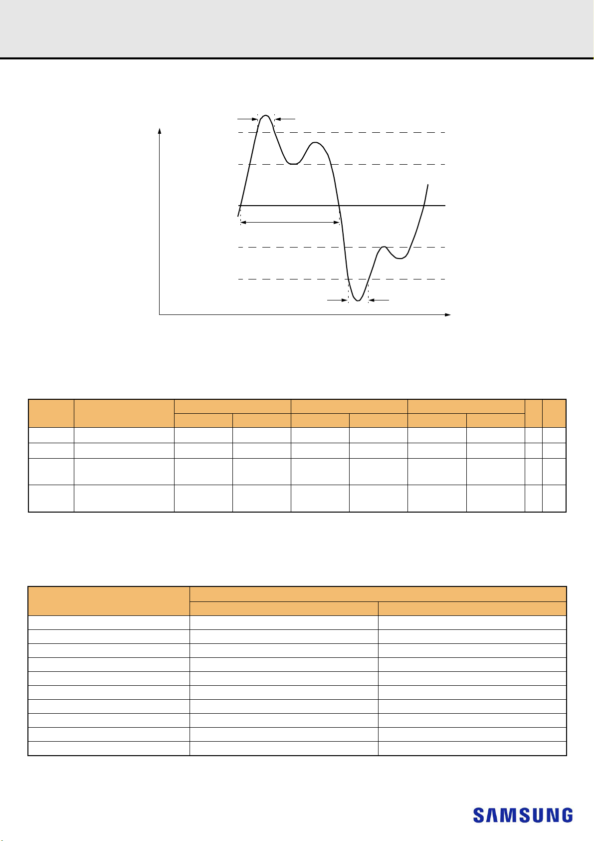
A
AOS1
V
DD
A
AUS
V
SS
Volts
(V)
1 tCK
V
AOSP
A
AOS2
V
AOS
V
AUS
Registered DIMM
datasheet
DDR4 SDRAM
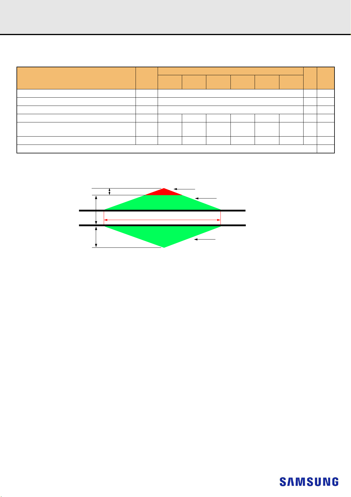
12.3.4 Address, Command and Control Overshoot and Undershoot specifications
[Table 11] AC overshoot/undershoot specification for Address, Command and Control pins
Specification
Parameter Symbol
Maximum peak amplitude above VAOS VAOSP 0.06 V
Upper boundary of overshoot area AAOS1 VAOS VDD +0.24 V 1
Maximum peak amplitude allowed for undershoot VAUS 0.30 V
Maximum overshoot area per 1 tCK above VAOS AAOS2 0.0083 0.0071 0.0062 0.0055 0.0055 0.0055 V-ns
Maximum overshoot area per 1 tCK between VDD and
VAOS
Maximum undershoot area per 1 tCK below VSS AAUS 0.2644 0.2265 0.1984 0.1762 0.1762 0.1762 V-ns
(A0-A13,A17,BG0-BG1,BA0-BA1,ACT_n,RAS_n/A16,CAS_n/A15,WE_n/A14,CS_n,CKE,ODT,C2-C0)
NOTE :
1) The value of VAOS matches VDD absolute max as defined in Table 5 Absolute Maximum DC Ratings if VDD equals VDD max as defined in Table 6 Recommended DC
Operating Conditions. If VDD is above the recommended operating conditions, VAOS remains at VDD absolute max as defined in Table 5.
AAOS1 0.2550 0.2185 0.1914 0.1699 0.1699 0.1699 V-ns
DDR4-
1600
DDR4-
1866
DDR4-
2133
DDR4-
2400
DDR4-
2666
DDR4-
2933
Unit NOTE
Figure 4. Address, Command and Control Overshoot and Undershoot Definition
- 21 -
Rev. 1.5
A
COS1
V
DD
A
CUS
V
SS
Volts
(V)
1 UI
V
COSP
A
COS2
V
COS
V
CUS
Registered DIMM
datasheet
DDR4 SDRAM
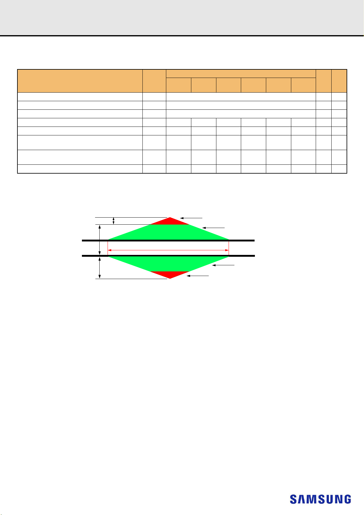
12.3.5 Clock Overshoot and Undershoot Specifications
[Table 12] AC overshoot/undershoot specification for Clock
Specification
Parameter Symbol
Maximum peak amplitude above VCOS VCOSP 0.06 V
Upper boundary of overshoot area ADOS1 VCOS VDD +0.24 V 1
Maximum peak amplitude allowed for undershoot VCUS 0.30 V
Maximum overshoot area per 1 UI above VCOS ACOS2 0.0038 0.0032 0.0028 0.0025 0.0025 0.0025 V-ns
Maximum overshoot area per 1 UI between VDD and
VDOS
Maximum undershoot area per 1 UI below VSS ACUS 0.1144 0.0980 0.0858 0.0762 0.0762 0.0762 V-ns
NOTE :
1) The value of VCOS matches VDD absolute max as defined in Table 5 Absolute Maximum DC Ratings if VDD equals VDD max as defined in Table 6 Recommended DC
Operating Conditions. If VDD is above the recommended operating conditions, VCOS remains at VDD absolute max as defined in Table 5.
ACOS1 0.1125 0.0964 0.0844 0.0750 0.0750 0.0750 V-ns
DDR4-
1600
(CK_t, CK_c)
DDR4-
1866
DDR4-
2133
DDR4-
2400
DDR4-
2666
DDR4-
2933
Unit NOTE
Figure 5. Clock Overshoot and Undershoot Definition
- 22 -
Rev. 1.5
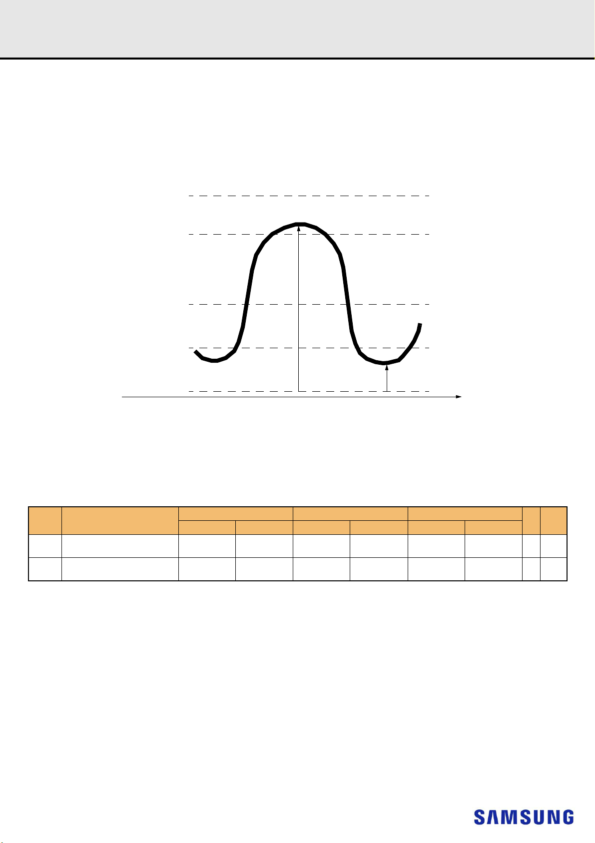
A
DOS1
V
DDQ
A
DUS2
V
SSQ
Volts
(V)
1 UI
V
DOSP
A
DOS2
V
DOS
V
DUSP
A
DUS1
Registered DIMM
datasheet
DDR4 SDRAM
12.3.6 Data, Strobe and Mask Overshoot and Undershoot Specifications
[Table 13] AC overshoot/undershoot specification for Data, Strobe and Mask
Specification
Parameter Symbol
Maximum peak amplitude above VDOS VDOSP 0.16 V
Upper boundary of overshoot area ADOS1 VDOS VDDQ + 0.24 V 1
Lower boundary of undershoot area ADUS1 VDUS 0.30 V 2
Maximum peak amplitude below VDUS VDUSP 0.10 0.10 0.10 0.10 0.10 0.10 V
Maximum overshoot area per 1 UI above VDOS ADOS2 0.0150 0.0129 0.0113 0.0100 0.0100 0.0100 V-ns
Maximum overshoot area per 1 UI between
VDDQ and VDOS
Maximum undershoot area per 1 UI between
VSSQ and VDUS1
Maximum undershoot area per 1 UI below VDUS ADUS2 0.0150 0.0129 0.0113 0.0100 0.0100 0.0100 V-ns
NOTE
:
1) The value of VDOS matches (VIN, VOUT) max as defined in Table 5 Absolute Maximum DC Ratings if VDDQ equals VDDQ max as defined in Table 6 Recommended DC
Operating Conditions. If VDDQ is above the recommended operating conditions, VDOS remains at (VIN, VOUT) max as defined in Table 5.
2) The value of VDUS matches (VIN, VOUT) min as defined in Table 5 Absolute Maximum DC Ratings
ADOS1 0.1050 0.0900 0.0788 0.0700 0.0700 0.0700 V-ns
ADUS1 0.1050 0.0900 0.0788 0.0700 0.0700 0.0700 V-ns
DDR4-
1600
DDR4-
1866
DDR4-
2133
DDR4-
2400
DDR4-
2666
DDR4-
2933
Unit
NOT
E
Figure 6. Data, Strobe and Mask Overshoot and Undershoot Definition
- 23 -
Rev. 1.5
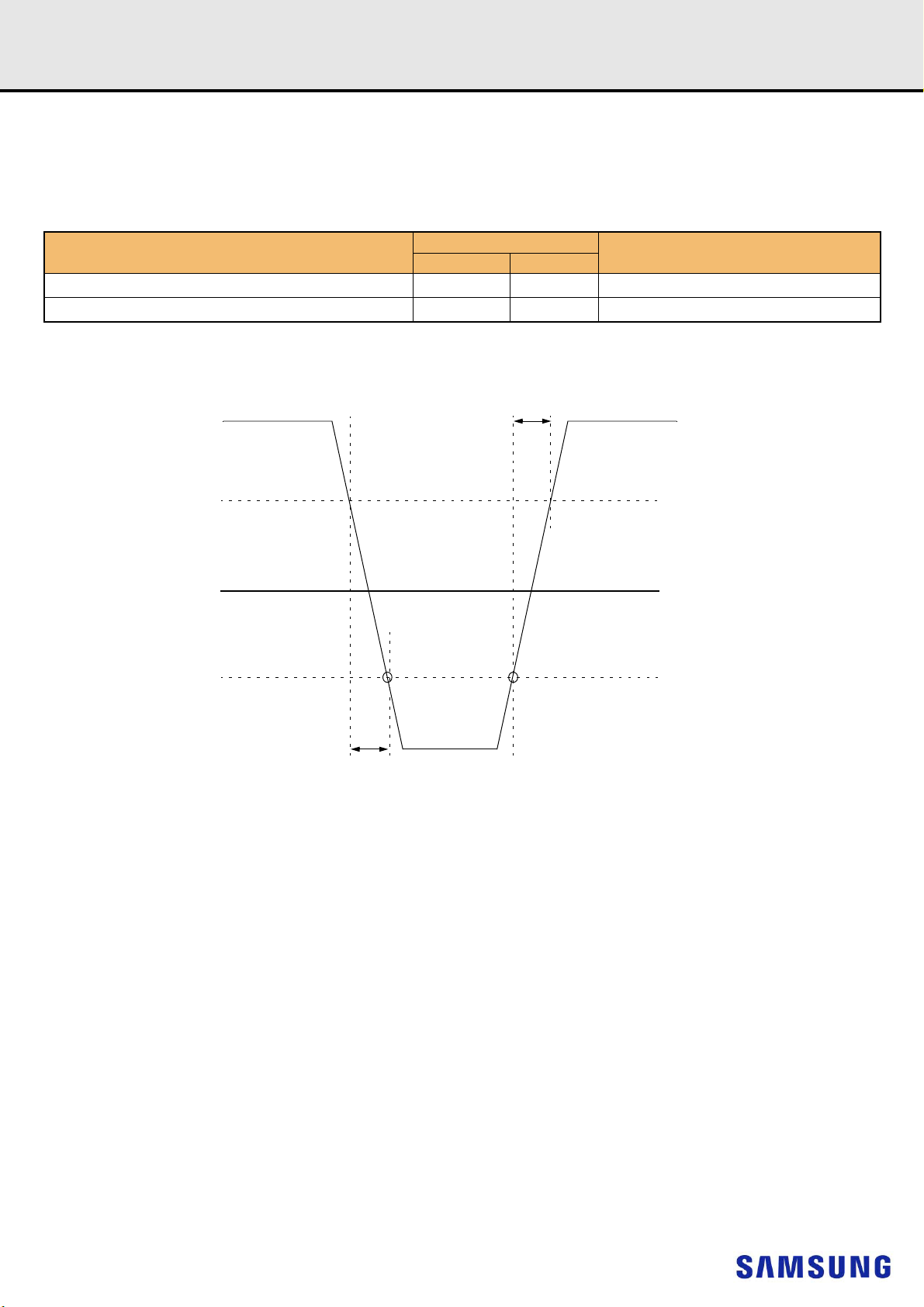
Delta TRdiff
Delta TFdiff
V
IHdiffmin
0
V
ILdiffmax
Differential Input Voltage(i,e, CK_t - CK_c)
Registered DIMM
datasheet
12.4 Slew Rate Definitions
12.4.1 Slew Rate Definitions for Differential Input Signals (CK)
Input slew rate for differential signals (CK_t, CK_c) are defined and measured as shown in Table 14 and Figure 7.
[Table 14] Differential Input Slew Rate Definition
Description
Differential input slew rate for rising edge (CK_t - CK_c)
Differential input slew rate for falling edge (CK_t - CK_c)
NOTE :
1) The differential signal (i,e.,CK_t - CK_c) must be linear between these thresholds.
Measured
from to
V
ILdiffmax
V
IHdiffmin
V
IHdiffmin
V
ILdiffmax
[V
[V
DDR4 SDRAM
Defined by
IHdiffmin
IHdiffmin
- V
- V
ILdiffmax
ILdiffmax
] / DeltaTRdiff
] / DeltaTFdiff
Figure 7. Differential Input Slew Rate Definition for CK_t, CK_c
- 24 -
Rev. 1.5
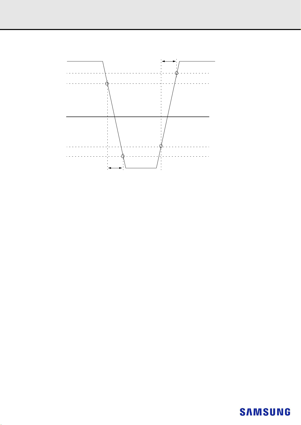
Delta TRsingle
Delta TFsingle
V
IHCA(AC) Min
V
IHCA(DC) Min
VREFCA(DC)
V
ILCA(DC) Max
V
ILCA(AC) Max
Registered DIMM
datasheet
12.4.2 Slew Rate Definition for Single-ended Input Signals (CMD/ADD)
DDR4 SDRAM
Figure 8. Single-ended Input Slew Rate definition for CMD and ADD
NOTE :
1) Single-ended input slew rate for rising edge = {VIHCA(AC)Min - VILCA(DC)Max} / Delta TR single.
2) Single-ended input slew rate for falling edge = {VIHCA(DC)Min - VILCA(AC)Max} / Delta TF single.
3) Single-ended signal rising edge from VILCA(DC)Max to VIHCA(DC)Min must be monotonic slope.
4) Single-ended signal falling edge from VIHCA(DC)Min to VILCA(DC)Max must be monotonic slope.
- 25 -
Rev. 1.5
Vix
CK_t
VDD/2
VSS
VDD
CK_c
Vix
VSEL
VSEH
Registered DIMM
datasheet
DDR4 SDRAM
12.5 Differential Input Cross Point Voltage
To guarantee tight setup and hold times as well as output skew parameters with respect to clock, each cross point voltage of differential input signals
(CK_t, CK_c) must meet the requirements in Table 15. The differential input cross point voltage VIX is measured from the actual cross point of true and
complement signals to the midlevel between of VDD and VSS.
Figure 9. Vix Definition (CK)
[Table 15] Cross Point Voltage for Differential Input Signals (CK)
Symbol Parameter
- Area of VSEH, VSEL
VlX(CK)
Symbol Parameter
VlX(CK)
Symbol Parameter
VlX(CK)
Differential Input Cross Point Voltage relative to
VDD/2 for CK_t, CK_c
- Area of VSEH, VSEL
Differential Input Cross Point Voltage relative to
VDD/2 for CK_t, CK_c
- Area of VSEH, VSEL
Differential Input Cross Point Voltage relative to
VDD/2 for CK_t, CK_c
VSEL < VDD/2 -
145mV
-120mV
VSEL <
VDD/2 - 145 mV
-120mV
VSEL <
VDD/2 - 145 mV
-110 mV
DDR4-1600/1866/2133
min max
VDD/2 - 145mV =<
VSEL =< VDD/2 -
100mV
-(VDD/2 - VSEL) +
25mV
min max
VDD/2 - 145 mV
=< VSEL =<
VDD/2 - 100 mV
- (VDD/2 - VSEL) +
25 mV
DDR4-2666/2933
min max
VDD/2 - 145 mV
=< VSEL =<
VDD/2 - 100 mV
- (VDD/2 - VSEL)
+ 30 mV
VDD/2 + 100mV =<
VSEH =< VDD/2 +
(VSEH - VDD/2) -
DDR4-2400
(VSEH - VDD/2) -
145mV
25mV
VDD/2 + 100 mV
=< VSEH =<
VDD/2 + 145 mV
25 mV
VDD/2 + 100 mV
=< VSEH =<
VDD/2 + 145 mV
(VSEH - VDD/2)
- 30 mV
VDD/2 + 145mV <
VSEH
120mV
VDD/2 + 145 mV <
VSEH
120mV
VDD/2 + 145 mV
< VSEH
110mV
- 26 -
Rev. 1.5
0.8*VDD
TR_RESET
tPW_RESET
0.7*VDD
0.3*VDD
0.2*VDD
Registered DIMM
datasheet
DDR4 SDRAM
12.6 CMOS rail to rail Input Levels
12.6.1 CMOS rail to rail Input Levels for RESET_n
[Table 16] CMOS rail to rail Input Levels for RESET_n
Parameter Symbol Min Max Unit NOTE
AC Input High Voltage VIH(AC)_RESET 0.8*VDD VDD V 6
DC Input High Voltage VIH(DC)_RESET 0.7*VDD VDD V 2
DC Input Low Voltage VIL(DC)_RESET VSS 0.3*VDD V 1
AC Input Low Voltage VIL(AC)_RESET VSS 0.2*VDD V 7
Rising time TR_RESET - 1.0 us 4
RESET pulse width tPW_RESET 1.0 - us 3,5
NOTE :
1) After RESET_n is registered LOW, RESET_n level shall be maintained below VIL(DC)_RESET during tPW_RESET, otherwise, SDRAM may not be reset.
2) Once RESET_n is registered HIGH, RESET_n level must be maintained above VIH(DC)_RESET, otherwise, SDRAM operation will not be guaranteed until it is reset
asserting RESET_n signal LOW.
3) RESET is destructive to data contents.
4) No slope reversal(ringback) requirement during its level transition from Low to High.
5) This definition is applied only “Reset Procedure at Power Stable”.
6) Overshoot might occur. It should be limited by the Absolute Maximum DC Ratings.
7) Undershoot might occur. It should be limited by Absolute Maximum DC Ratings.
Figure 10. RESET_n Input Slew Rate Definition
- 27 -
Rev. 1.5
Registered DIMM
datasheet
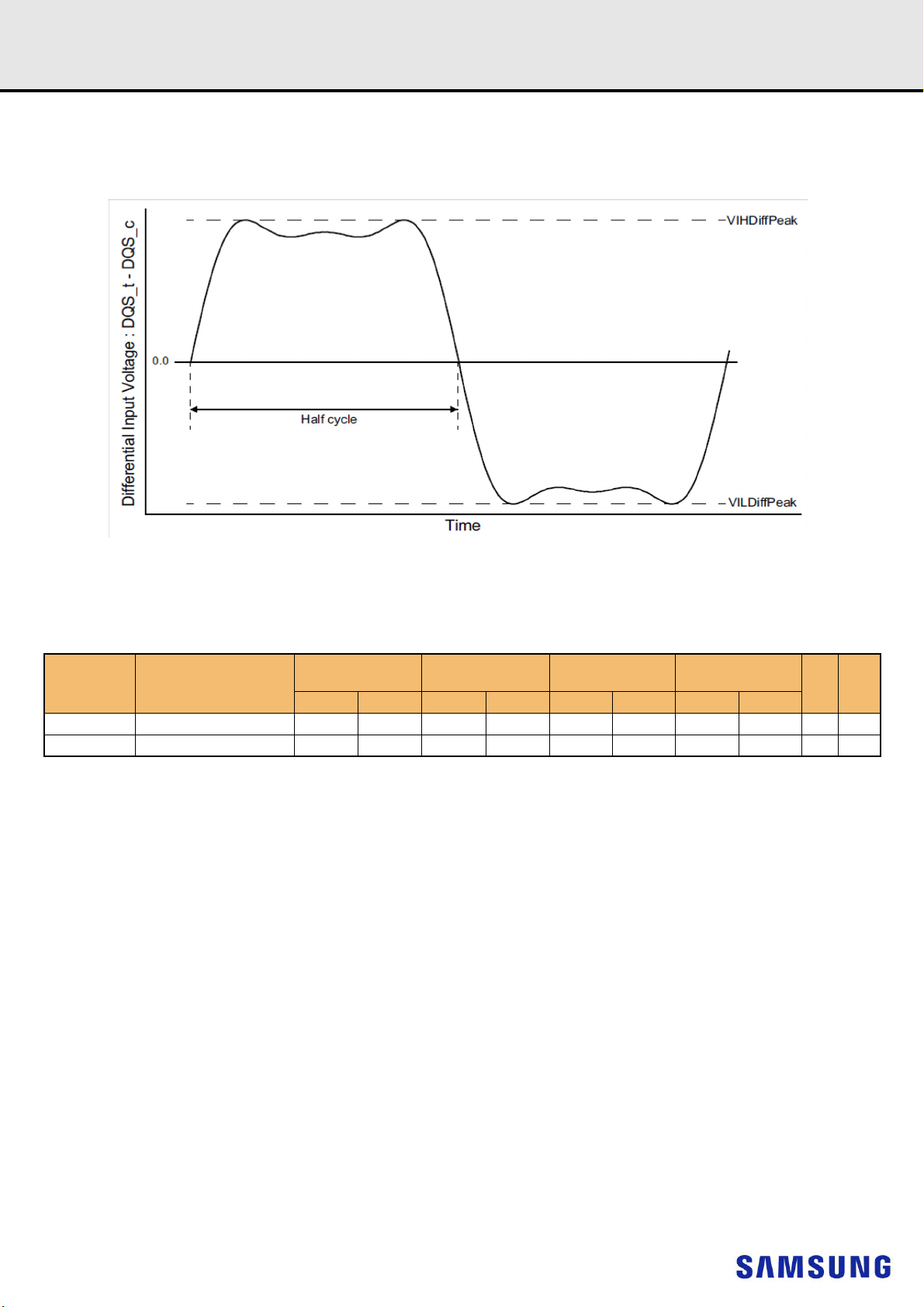
12.7 AC and DC Logic Input Levels for DQS Signals
12.7.1 Differential signal definition
DDR4 SDRAM
Figure 11. Definition of differential DQS Signal AC-swing Level
12.7.2 Differential swing requirements for DQS (DQS_t - DQS_c)
[Table 17] Differential AC and DC Input Levels for DQS
DDR4-1600, 1866,
Symbol Parameter
VIHDiffPeak VIH.DIFF.Peak Voltage 186 Note2 160 Note2 150 Note2 145 Note2 mV 1
VILDiffPeak VIL.DIFF.Peak Voltage Note2 -186 Note2 -160 Note2 -150 Note2 -145 mV 1
NOTE :
1) Used to define a differential signal slew-rate.
2) These values are not defined; however, the differential signals DQS_t - DQS_c, need to be within the respective limits Overshoot, Undershoot Specification for single-ended
signals.
2133
Min Max Min Max Min Max Min Max
DDR4-2400 DDR4-2666
DDR4-2933
Unit Note
- 28 -
 Loading...