

Page 1

PLC2/30 Programmable Controller
Programming and Operations Manual
Page 2
Important User Information
Because of the variety of uses for this equipment and because of the
differences between this solid state equipment and electromechanical
equipment, the user of and those responsible for applying this equipment
must satisfy themselves as to the acceptability of each application and
use of the equipment. In no event will Allen-Bradley Company, Inc. be
responsible or liable for indirect or consequential damages resulting from
the use or application of this equipment.
The illustrations, charts, and layout examples shown in this manual are
intended solely to illustrate the text of this manual. Because of the many
variables and requirements associated with any particular installation,
Allen-Bradley Company, Inc. cannot assume responsibility or liability for
actual use based upon the illustrative uses and applications.
No patent liability is assumed by Allen-Bradley Company, Inc. with
respect to use of information, circuits, equipment or software described in
this text.
Reproduction of the contents of this manual, in whole or in part, without
written permission of the Allen-Bradley Company, Inc. is prohibited.
1988 Allen-Bradley Company, Inc.
PLC is a registered trademark of Allen-Bradley Company, Inc.
WARNING: Warnings tell readers where people may be hurt if
procedures are not followed properly.
CAUTION: Cautions tell them where machinery may be
damaged or economic loss can occur if procedures are not
followed properly.
A Warning or Caution alerts you to:
a possible trouble spot
what causes the trouble to occur
the result of an improper action
how to avoid the situation
Page 3

Table of Contents
Introduction 11. . . . . . . . . . . . . . . . . . . . . . . . . . . . . . . . . . . .
1.0 Introduction to This Manual 11. . . . . . . . . . . . . . . . . . . . . . . . . .
1.1 General 11
1.2
Capabilities
1.2.1
Complementary I/O
Data Highway Compatibility
1.2.2
1.2.3 Industrial T
1.3
Additional Publications
1.4 Terms Used in This Manual 16
Hardware Considerations 21. . . . . . . . . . . . . . . . . . . . . . . . .
2.0 General 21. . . . . . . . . . . . . . . . . . . . . . . . . . . . . . . . . . . . . . . .
Mode Select Switch
2.1
2.2 Memory Write Protect 22
2.3 RunTime Errors 23
2.4 Processor Diagnostic Indicators 24
2.5 PowerUp Recovery 25
2.6 Switch Group Assembly 25
Last State Switch
2.6.1
2.6.2 I/O Rack Number 26
2.7 Industrial Terminal 27
2.8 Local System Structure 27
2.9 Remote System Structure 28
2.10 Local/Remote System Structure 29
2.11 Hardware Addressing Modes 210
2.12 Auxiliary Power Supplies 210
2.12.1 1771P2 Auxiliary Power Supply 210
2.12.2 1777P2 Auxiliary Power Supply 211
2.12.3 1771P3, P4, and P5 Slot Power Supplies 211
2.12.4 1771P7 Power Supply 211
2.12.5 1771PSC Power Supply Chassis 211
. . . . . . . . . . . . . . . . . . . . . . . . . . . . . . . . . . . . . . . .
erminal Compatibility
. . . . . . . . . . . . . . . . . . . . . . . . . .
. . . . . . . . . . . . . . . . . . . . . . . . . . . . . .
. . . . . . . . . . . . . . . . . . . . . . . . . . . . . . . . . .
. . . . . . . . . . . . . . . . . . . . . . .
. . . . . . . . . . . . . . . . . . . . . . . . . . . . . . .
. . . . . . . . . . . . . . . . . . . . . . . . . . . .
. . . . . . . . . . . . . . . . . . . . . . . . . . . . . . . .
. . . . . . . . . . . . . . . . . . . . . . . . . . . . . . . .
. . . . . . . . . . . . . . . . . . . . . . . . . . . . .
. . . . . . . . . . . . . . . . . . . . . . . . . . .
. . . . . . . . . . . . . . . . . . . . . .
. . . . . . . . . . . . . . . . . . . . . . . .
. . . . . . . . . . . . . . . . . . . . . . . . . . .
. . . . . . . . . . . . . . . . . . . .
. . . . . . . . . . . . . . . . . . . .
. . . . . . . . . . . .
. . . . . . . . . . . . . . . . . . . . . . . . . . .
. . . . . . . . . . . . . . . . . . .
13. . . . . . . . . . . . . . . . . . . . . . . . . . . . . . . . . . . . .
14. . . . . . . . . . . . . . . . . . . . . . . . . . . . . .
14. . . . . . . . . . . . . . . . . . . . . . . . .
14. . . . . . . . . . . . . . . . . . . . .
15. . . . . . . . . . . . . . . . . . . . . . . . . . . . .
21. . . . . . . . . . . . . . . . . . . . . . . . . . . . . . .
26. . . . . . . . . . . . . . . . . . . . . . . . . . . . . . . .
Data Table 31. . . . . . . . . . . . . . . . . . . . . . . . . . . . . . . . . . . . .
3.0 General 31. . . . . . . . . . . . . . . . . . . . . . . . . . . . . . . . . . . . . . . .
3.1 Memory Structure 31
3.2 Memory Organization 32
3.2.1 Data Table 32
3.2.2 User Program 316
3.2.3 Message Storage Area 317
3.3 Hardware/Program Interface 317
3.3.1 Image Tables 317
. . . . . . . . . . . . . . . . . . . . . . . . . . . . . . . . .
. . . . . . . . . . . . . . . . . . . . . . . . . . . . . .
. . . . . . . . . . . . . . . . . . . . . . . . . . . . . . . . . . . . .
. . . . . . . . . . . . . . . . . . . . . . . . . . . . . . . . . .
. . . . . . . . . . . . . . . . . . . . . . . . . . . .
. . . . . . . . . . . . . . . . . . . . . . . . .
. . . . . . . . . . . . . . . . . . . . . . . . . . . . . . . . . . .
Page 4

Table of Contentsii
3.3.2 Instruction Address 318. . . . . . . . . . . . . . . . . . . . . . . . . . . . . .
3.3.3 Fundamental Operation 321
3.4 Data Table Documentation Forms 323
3.4.1 Data Table Word Map (1024 Word) 323
3.4.2 Data Table Map (128 Word) 324
3.4.3 Data Table Word Assignments (64 Word) 325
3.4.4 Data T
3.4.5 Sequencer T
3.4.6
3.4.7 Timer/Counter Assignments 329
3.4.8 Data Storage Assignments 329
able Bit Assignments
able Bit Assignments
I/O Assignments
. . . . . . . . . . . . . . . . . . . . . . . . . . .
. . . . . . . . . . . . . . . . . . . . .
. . . . . . . . . . . . . . . . . . .
. . . . . . . . . . . . . . . . . . . . . . . .
. . . . . . . . . . . . . . .
326. . . . . . . . . . . . . . . . . . . . . . . .
327. . . . . . . . . . . . . . . . . . . .
328. . . . . . . . . . . . . . . . . . . . . . . . . . . . . . . .
. . . . . . . . . . . . . . . . . . . . . . . .
. . . . . . . . . . . . . . . . . . . . . . . . .
Introduction
4.0 General 41. . . . . . . . . . . . . . . . . . . . . . . . . . . . . . . . . . . . . . . .
4.1
Notational Conventions
4.2 Ladder Diagram Logic 42
4.3 RelayType Instructions 43
4.3.1 Examine Instructions 43
Output Instructions
4.3.2
4.3.3 Branch Instructions 49
4.3.4 Ending a Program 412
4.3.5 Programming RelayType Instructions 413
4.4 Operating Instructions 414
4.4.1 Addressing 415
4.4.2 Help Directories 415
4.4.3 Searching 416
4.4.4
Editing
4.4.5 OnLine Programming 423
4.4.6 Clearing Memory 430
4.5 Program Recommendations 432
to Programming
. . . . . . . . . . . . . . . . . . . . . . . . . . . . . .
. . . . . . . . . . . . . . . . . . . . . . . . . . . . .
. . . . . . . . . . . . . . . . . . . . . . . . . . . . .
. . . . . . . . . . . . . . . . . . . . . . . . . . . . . .
. . . . . . . . . . . . . . . . . . . . . . . . . . . . . . .
. . . . . . . . . . . . . . . . .
. . . . . . . . . . . . . . . . . . . . . . . . . . . . . .
. . . . . . . . . . . . . . . . . . . . . . . . . . . . . . . . . . . .
. . . . . . . . . . . . . . . . . . . . . . . . . . . . . . . . .
. . . . . . . . . . . . . . . . . . . . . . . . . . . . . . . . . . . . .
. . . . . . . . . . . . . . . . . . . . . . . . . . . .
. . . . . . . . . . . . . . . . . . . . . . . . . . . . . . . .
. . . . . . . . . . . . . . . . . . . . . . . . .
41. . . . . . . . . . . . . . . . . . . . . . .
41. . . . . . . . . . . . . . . . . . . . . . . . . . . . .
45. . . . . . . . . . . . . . . . . . . . . . . . . . . . . . .
419. . . . . . . . . . . . . . . . . . . . . . . . . . . . . . . . . . . . . . .
Timer and Counter Instructions 51. . . . . . . . . . . . . . . . . . . . .
5.0 General 51. . . . . . . . . . . . . . . . . . . . . . . . . . . . . . . . . . . . . . . .
5.1 Timer Instructions 52
5.1.1 Timer OnDelay Instruction 53
5.1.2 T
imer Of
fDelay Instruction 55. . . . . . . . . . . . . . . . . . . . . . . . .
5.1.3
Retentive T
Retentive T
5.1.4
5.1.5 Timer Accuracy for 10ms Timers 58
5.2 Counter Instructions 58
5.2.1 UpCounter Instruction 59
5.2.2 Counter Reset Instruction 511
5.2.3 DownCounter Instruction 512
5.2.4 Scan Counter Instruction 513
5.3 Cascading Timers or Counters 514
. . . . . . . . . . . . . . . . . . . . . . . . . . . . . . . . .
. . . . . . . . . . . . . . . . . . . . . . . . .
imer Instruction 56. . . . . . . . . . . . . . . . . . . . . . . . .
imer Reset Instruction 58. . . . . . . . . . . . . . . . . . . .
. . . . . . . . . . . . . . . . . . . . .
. . . . . . . . . . . . . . . . . . . . . . . . . . . . . . .
. . . . . . . . . . . . . . . . . . . . . . . . . . . .
. . . . . . . . . . . . . . . . . . . . . . . . . .
. . . . . . . . . . . . . . . . . . . . . . . . . .
. . . . . . . . . . . . . . . . . . . . . . . . . .
. . . . . . . . . . . . . . . . . . . . . . . .
Page 5

Table of Contents iii
5.4 Programming Timer and Counter Instructions 514. . . . . . . . . . . . .
5.5 Scan Time and Instruction Execution Times 517
5.5.1 Scan Time 517
5.5.2 Program for Determining Scan Time 518
5.6 Instruction Execution Time 519
5.6.1 Relay Type, Timer and Counter
Arithmetic, Output Override and I/O Update, Jump, and
Subroutine Instructions 519. . . . . . . . . . . . . . . . . . . . . . . . . . . . .
5.6.2
WordtoFile, Sequencers, FIFO, W
Diagnostic, File Search, and Block Transfer Instructions 520. . . . . .
FiletoFile Move and File Complement
5.6.3
5.6.4
Logic Instructions FiletoFile AND, OR, XOR
. . . . . . . . . . . . . . . . . . . . . . . . . . . . . . . . . . . . .
. . . . . . . . . . . . . . . . . . . . . . . . . . .
, Data Manipulations,
ord and Bit Shifts, File
. . . . . . . . . . . . . .
. . . . . . . . . . . . . . . . . .
522. . . . . . . . . . . . . . . .
523. . . . . . . . . . . .
Data Manipulation Instructions 61. . . . . . . . . . . . . . . . . . . . .
6.0 General 61. . . . . . . . . . . . . . . . . . . . . . . . . . . . . . . . . . . . . . . .
6.1 Data Transfer Instructions 62
6.1.1
Get Instruction
Put Instruction
6.1.2
6.2 Data Comparison Instructions 64
6.2.1 Les and Equ Instructions 64
6.2.2
Get Byte and Limit T
6.2.3
Get Byte-Put Instruction
6.3 Programming Data Manipulation Instructions 69
Arithmetic Instructions
6.4
6.4.1 Add Instruction 612
6.4.2 Subtract Instruction 613
6.4.3
Multiply Instruction
6.4.4
Divide Instruction
6.5 Programming Arithmetic Instructions 615
6.6 BCD to Binary Conversion 616
6.6.1 Programming a BCD to Binary Conversion Instruction 617
6.7 BinarytoBCD Conversion 618
6.7.1 Programming a Binaryto BCD Conversion Instruction 618
. . . . . . . . . . . . . . . . . . . . . . . . . . . . . . . . .
. . . . . . . . . . . . . . . . . . . . . . . . . . .
62. . . . . . . . . . . . . . . . . . . . . . . . . . . . . . . . . .
63. . . . . . . . . . . . . . . . . . . . . . . . . . . . . . . . . .
. . . . . . . . . . . . . . . . . . . . . . . .
. . . . . . . . . . . . . . . . . . . . . . . . . .
est Instructions 67. . . . . . . . . . . . . . . . . . .
68. . . . . . . . . . . . . . . . . . . . . . . . . . .
. . . . . . . . . . . . . .
611. . . . . . . . . . . . . . . . . . . . . . . . . . . . . .
. . . . . . . . . . . . . . . . . . . . . . . . . . . . . .
614. . . . . . . . . . . . . . . . . . . . . . . . . . . . . . .
614. . . . . . . . . . . . . . . . . . . . . . . . . . . . . . . .
. . . . . . . . . . . . . . . . . . .
. . . . . . . . . . . . . . . . . . . . . . . . . . .
. . . . . .
. . . . . . . . . . . . . . . . . . . . . . . . . .
. . . . .
Output Override and I/O Update Instructions 71. . . . . . . . . . .
7.0 General 71. . . . . . . . . . . . . . . . . . . . . . . . . . . . . . . . . . . . . . . .
7.1 Output Overrides 71
7.2
I/O Updates
7.2.1 Scan Sequence 73
7.2.2
Immediate Input Instruction
7.2.3
Immediate Output Instruction
7.3
Programming Immediate I/O Instructions
7.4 Remote Fault Zone Programming 79
7.4.1 Dependent Programming 712
. . . . . . . . . . . . . . . . . . . . . . . . . . . . . . . . .
73. . . . . . . . . . . . . . . . . . . . . . . . . . . . . . . . . . . . .
. . . . . . . . . . . . . . . . . . . . . . . . . . . . . . . . .
75. . . . . . . . . . . . . . . . . . . . . . . . .
76. . . . . . . . . . . . . . . . . . . . . . . .
78. . . . . . . . . . . . . . . . .
. . . . . . . . . . . . . . . . . . . . . .
. . . . . . . . . . . . . . . . . . . . . . . . . .
Page 6

Table of Contentsiv
7.4.2 Independent Programming 713. . . . . . . . . . . . . . . . . . . . . . . . .
7.5
I/O Update T
7.5.1 Local Systems 715
7.5.2 Remote Systems 715
7.6 Watchdog Timer 716
imes 715. . . . . . . . . . . . . . . . . . . . . . . . . . . . . . . . .
. . . . . . . . . . . . . . . . . . . . . . . . . . . . . . . . . .
. . . . . . . . . . . . . . . . . . . . . . . . . . . . . . . .
. . . . . . . . . . . . . . . . . . . . . . . . . . . . . . . . . .
Peripheral Functions 81. . . . . . . . . . . . . . . . . . . . . . . . . . . . .
8.0 General 81. . . . . . . . . . . . . . . . . . . . . . . . . . . . . . . . . . . . . . . .
8.1
Communication Rate Setting
8.2 Contact Histogram 82
8.3 Digital Cassette Recorder 84
8.3.1 Dumping Memory Content to Cassette Tape 84
8.3.2 Loading Memory from Cassette Tape 84
8.3.3 Verification 85
8.3.4 Program Verification 85
8.3.5 Displaying and Locating Errors 86
8.4 Data Cartridge Recorder 86
8.4.1 Dumping Memory Content onto Data Cartridge Tape 86
8.4.2 Loading Memory from a Data Cartridge Tape 87
8.4.3 Data Cartridge Verification 88
8.5 Ladder Diagram Dump 88
8.6 Total Memory Dump 88
. . . . . . . . . . . . . . . . . . . . . . . . . . . . . . . .
. . . . . . . . . . . . . . . . . . . . . . . . . . .
. . . . . . . . . . . . .
. . . . . . . . . . . . . . . . . .
. . . . . . . . . . . . . . . . . . . . . . . . . . . . . . . . . . . .
. . . . . . . . . . . . . . . . . . . . . . . . . . . . . .
. . . . . . . . . . . . . . . . . . . . . .
. . . . . . . . . . . . . . . . . . . . . . . . . . . .
. . . . . . .
. . . . . . . . . . . .
. . . . . . . . . . . . . . . . . . . . . . . . .
. . . . . . . . . . . . . . . . . . . . . . . . . . . . .
. . . . . . . . . . . . . . . . . . . . . . . . . . . . . . .
81. . . . . . . . . . . . . . . . . . . . . . . . .
Report Generation 91. . . . . . . . . . . . . . . . . . . . . . . . . . . . . . .
9.0 General 91. . . . . . . . . . . . . . . . . . . . . . . . . . . . . . . . . . . . . . . .
9.1 Report Generation Commands 93
9.1.1 Message Control Word File - MS, 0 94
9.1.2 Message Store - MS 95
9.1.3 Message Print - MP 96
9.1.4 Message Report - MR 97
9.1.5 Message Delete - MD 97
9.1.6 Message Index - MI 97
9.1.7 Control Codes and Special Commands 97
9.2
Manually Initiated Report Generation
9.3 Automatic Report Generation 912
9.3.1 Messages 16 913
9.3.2 Additional Messages 913
9.3.3 Example Programming 914
. . . . . . . . . . . . . . . . . . . . . . . . . . . . .
. . . . . . . . . . . . . . . . . . . . . . . . . . . . . .
. . . . . . . . . . . . . . . . . . . . . . . . . . . . . .
. . . . . . . . . . . . . . . . . . . . . . . . . . . . . . . . . .
. . . . . . . . . . . . . . . . . . . . . . . . . . . . .
. . . . . . . . . . . . . . . . . . . . . . .
. . . . . . . . . . . . . . . . . . .
. . . . . . . . . . . . . . . . . . . . . . . . . . . .
. . . . . . . . . . . . . . . . . . . . . . . . . . . .
. . . . . . . . . . . . . . . .
911. . . . . . . . . . . . . . . . . . .
. . . . . . . . . . . . . . . . . . . . . . . . .
. . . . . . . . . . . . . . . . . . . . . . . . . . . .
Block Transfer 101. . . . . . . . . . . . . . . . . . . . . . . . . . . . . . . . . .
10.0 General 101. . . . . . . . . . . . . . . . . . . . . . . . . . . . . . . . . . . . . . .
10.1 Basic Operation 101
10.2 Block Transfer Instructions 104
10.2.1 Data Address and Module Address 104
. . . . . . . . . . . . . . . . . . . . . . . . . . . . . . . . .
. . . . . . . . . . . . . . . . . . . . . . . . .
. . . . . . . . . . . . . . . . . .
Page 7

Table of Contents v
10.2.2 Block Length 105. . . . . . . . . . . . . . . . . . . . . . . . . . . . . . . . . .
10.2.3 File Address 105
10.2.4
Enable Bit and Done Bit
10.3 Instruction Notes for Block Transfer Read and
Write Instructions 106
10.4 Causes of RunTime Errors 106
10.5 Programming Block Transfer Read and Write Instructions 106
10.6
Multiple Reads of Dif
10.7
Defining the Block T
10.8
Buf
fering Data 1012. . . . . . . . . . . . . . . . . . . . . . . . . . . . . . . . . .
10.9 Bidirectional Block Transfer 1014
10.9.1 Operation 1014
10.9.2 Data Address and Module Address 1017
10.9.3 File Address 1017
10.9.4 Block Length 1017
10.9.5 Programming Considerations 1018
. . . . . . . . . . . . . . . . . . . . . . . . . . . . . . . . . .
106. . . . . . . . . . . . . . . . . . . . . . . . . .
. . . . . . . . . . . . . . . . . . . . . . . . . . . . . . . . .
. . . . . . . . . . . . . . . . . . . . . . . . .
. . .
ferent Block Lengths from One Module 108. .
ransfer Data Address Area 1011. . . . . . . . . . .
. . . . . . . . . . . . . . . . . . . . . . . . .
. . . . . . . . . . . . . . . . . . . . . . . . . . . . . . . . . . . .
. . . . . . . . . . . . . . . . . .
. . . . . . . . . . . . . . . . . . . . . . . . . . . . . . . . . .
. . . . . . . . . . . . . . . . . . . . . . . . . . . . . . . . . .
. . . . . . . . . . . . . . . . . . . . . .
Jump Instructions and
11.0 General 111. . . . . . . . . . . . . . . . . . . . . . . . . . . . . . . . . . . . . . .
11.1 Jump Instruction 111
11.1.1 Programming Jump/ Subroutine Instructions 113
11.1.2
Multiple Jumps to the Same Label
11.2 Label Instruction 116
11.3 Jump to Subroutine Instruction 117
11.3.1 Subroutine Area 1110
11.3.2 Nested Subroutines 1111
11.3.3 Recursive Subroutine (Looping) Calls 1112
11.3.4 Subroutine Programming Considerations 1112
11.4 Return Instruction 1114
Subroutine Programming
. . . . . . . . . . . . . . . . . . . . . . . . . . . . . . . . .
. . . . . . . . . . . .
. . . . . . . . . . . . . . . . . . . . . . . . . . . . . . . . .
. . . . . . . . . . . . . . . . . . . . . . .
. . . . . . . . . . . . . . . . . . . . . . . . . . . . . . . .
. . . . . . . . . . . . . . . . . . . . . . . . . . . . .
. . . . . . . . . . . . . . . .
. . . . . . . . . . . . . .
. . . . . . . . . . . . . . . . . . . . . . . . . . . . . . . .
111. . . . . . . .
113. . . . . . . . . . . . . . . . . . .
Data Transfer File Instructions 121. . . . . . . . . . . . . . . . . . . . . .
12.0 General 121. . . . . . . . . . . . . . . . . . . . . . . . . . . . . . . . . . . . . . .
12.1 File Concepts 121
12.1.1
File Definition
12.1.2
File Planning
12.1.3
File Instructions
12.1.4 Programming File Instructions 1211
12.1.5 File Instruction RunTime Error 1212
12.2 FiletoFile Move 1212
12.2.1 Programming FiletoFile Move Instructions 1214
12.3 FiletoWord Move 1215
12.3.1 Programming FiletoWord Move Instructions 1216
12.4 WordtoFile Move 1218
12.4.1 Programming WordtoFile Move Instructions 1219
12.5 Data Monitor Mode 1221
. . . . . . . . . . . . . . . . . . . . . . . . . . . . . . . . . . .
121. . . . . . . . . . . . . . . . . . . . . . . . . . . . . . . . . .
122. . . . . . . . . . . . . . . . . . . . . . . . . . . . . . . . . .
122. . . . . . . . . . . . . . . . . . . . . . . . . . . . . . . .
. . . . . . . . . . . . . . . . . . . . . .
. . . . . . . . . . . . . . . . . . . . .
. . . . . . . . . . . . . . . . . . . . . . . . . . . . . . . . .
. . . . . . . . . . . .
. . . . . . . . . . . . . . . . . . . . . . . . . . . . . . .
. . . . . . . . . . .
. . . . . . . . . . . . . . . . . . . . . . . . . . . . . . .
. . . . . . . . . . .
. . . . . . . . . . . . . . . . . . . . . . . . . . . . . . .
Page 8

Table of Contentsvi
12.5.1 Accessing the Data Monitor Mode 1221. . . . . . . . . . . . . . . . . . .
12.5.2
Data Monitor Display
12.5.3 Cursor Controls 1225
12.5.4 Data Monitoring Procedures 1226
12.5.5 Entering and Changing Data 1227
. . . . . . . . . . . . . . . . . . . . . . . . . . . . . . . .
. . . . . . . . . . . . . . . . . . . . . . .
. . . . . . . . . . . . . . . . . . . . . . .
1224. . . . . . . . . . . . . . . . . . . . . . . . . . . .
Shift Register Instructions 131. . . . . . . . . . . . . . . . . . . . . . . . .
13.0 General 131. . . . . . . . . . . . . . . . . . . . . . . . . . . . . . . . . . . . . . .
13.1
Shift File Up
13.1.1
Programming Shift File Up Instruction
13.2
Shift File Down
13.2.1
Programming Shift File Down Instruction
13.3 FIFO Load and FIFO Unload 136
13.3.1 Programming FIFO Load and FIFO Unload Instruction 138
. . . . . . . . . . . . . . . . . . . . . . . .
. . . . .
132. . . . . . . . . . . . . . . . . . . . . . . . . . . . . . . . . . . .
133. . . . . . . . . . . . . . . .
135. . . . . . . . . . . . . . . . . . . . . . . . . . . . . . . . . .
135. . . . . . . . . . . . . .
Bit Shifts 141. . . . . . . . . . . . . . . . . . . . . . . . . . . . . . . . . . . . . .
14.0 General 141. . . . . . . . . . . . . . . . . . . . . . . . . . . . . . . . . . . . . . .
14.1
Bit Shift Left
14.1.1
Programming Bit Shift Left Instruction
Bit Shift Right
14.2
14.2.1
Programming Bit Shift Right Instruction
14.3
Examine Of
14.3.1 Programming Examine Of
14.4
Examine On Shift Bit
14.4.1
Programming Examine On Shift Bit Instruction
Set Shift Bit
14.5
14.5.1
Programming Set Shift Bit Instruction
14.6
Reset Shift Bit
14.6.1
Programming Reset Shift Bit Instruction
f Shift Bit
f Shift Bit Instruction
141. . . . . . . . . . . . . . . . . . . . . . . . . . . . . . . . . . . .
143. . . . . . . . . . . . . . . . .
145. . . . . . . . . . . . . . . . . . . . . . . . . . . . . . . . . . .
146. . . . . . . . . . . . . . .
146. . . . . . . . . . . . . . . . . . . . . . . . . . . . . .
146. . . . . . . . . .
148. . . . . . . . . . . . . . . . . . . . . . . . . . . . . .
148. . . . . . . . . .
149. . . . . . . . . . . . . . . . . . . . . . . . . . . . . . . . . . . .
149. . . . . . . . . . . . . . . . .
1410. . . . . . . . . . . . . . . . . . . . . . . . . . . . . . . . . . .
1411. . . . . . . . . . . . . . .
Sequencer Instructions 151. . . . . . . . . . . . . . . . . . . . . . . . . . .
15.0 General 151. . . . . . . . . . . . . . . . . . . . . . . . . . . . . . . . . . . . . . .
15.1 Sequencer Output Instruction 153
15.1.1 Sequencer Output Analogy 153
15.1.2 Operation of the Sequencer Output Instruction 154
15.1.3
Masking Output Data
15.1.4 Instruction Overview 156
15.1.5 Programming the Sequencer Output Instruction 156
15.2 Sequencer Input Instruction 1510
15.2.1 Operation of the Sequencer Input Instruction 1510
15.2.2 Masking Input Data 1510
15.2.3 Instruction Overview 1510
15.2.4 Programming the Sequencer Input Instruction 1511
15.3 Sequencer Load Instruction 1513
. . . . . . . . . . . . . . . . . . . . . . . .
. . . . . . . . . . . . . . . . . . . . . . . .
. . . . . . . . . .
155. . . . . . . . . . . . . . . . . . . . . . . . . . . .
. . . . . . . . . . . . . . . . . . . . . . . . . . . . .
. . . . . . . . .
. . . . . . . . . . . . . . . . . . . . . . . . .
. . . . . . . . . . .
. . . . . . . . . . . . . . . . . . . . . . . . . . . . .
. . . . . . . . . . . . . . . . . . . . . . . . . . . . .
. . . . . . . . . . .
. . . . . . . . . . . . . . . . . . . . . . . . .
Page 9

Table of Contents vii
15.3.1 Operation of the Sequencer Load Instruction 1513. . . . . . . . . . .
15.3.2 Instruction Overview 1514
15.3.3 Programming the Sequencer Load Instruction 1514
. . . . . . . . . . . . . . . . . . . . . . . . . . . . .
. . . . . . . . . .
File Logic Instructions 161. . . . . . . . . . . . . . . . . . . . . . . . . . . .
16.0 General 161. . . . . . . . . . . . . . . . . . . . . . . . . . . . . . . . . . . . . . .
16.1 FiletoFile Logic Instructions 161
16.1.1
FiletoFile AND
16.1.2
FiletoFile OR
16.1.3
FiletoFile XOR
16.1.4
File Complement
16.2 WordtoFile Logic Instructions 168
16.2.1 WordtoFile AND 169
16.2.2 WordtoFile OR 1611
16.2.3 WordtoFile XOR 1612
. . . . . . . . . . . . . . . . . . . . . . . . . . . . . . .
. . . . . . . . . . . . . . . . . . . . . . . . . . . . . . . .
. . . . . . . . . . . . . . . . . . . . . . . . . . . . . .
. . . . . . . . . . . . . . . . . . . . . . . .
162. . . . . . . . . . . . . . . . . . . . . . . . . . . . . . . .
164. . . . . . . . . . . . . . . . . . . . . . . . . . . . . . . . .
165. . . . . . . . . . . . . . . . . . . . . . . . . . . . . . . .
166. . . . . . . . . . . . . . . . . . . . . . . . . . . . . . .
. . . . . . . . . . . . . . . . . . . . . . .
File Search and File Diagnostic Instructions 171. . . . . . . . . . .
17.0 General 171. . . . . . . . . . . . . . . . . . . . . . . . . . . . . . . . . . . . . . .
17.1 File Search 171
File Diagnostics
17.2
. . . . . . . . . . . . . . . . . . . . . . . . . . . . . . . . . . . . .
174. . . . . . . . . . . . . . . . . . . . . . . . . . . . . . . . .
Troubleshooting Aids 181. . . . . . . . . . . . . . . . . . . . . . . . . . . .
18.0 General 181. . . . . . . . . . . . . . . . . . . . . . . . . . . . . . . . . . . . . . .
18.1
Bit Manipulation and Monitor
18.1.1
Bit Manipulation
18.1.2
Bit Monitor
18.2 Force On and Force Off Functions 183
18.3 Forced Address Display 184
18.4 Temporary End Instruction 185
18.5 ERR Message for an Illegal OP Code 185
Special
19.0 General 191. . . . . . . . . . . . . . . . . . . . . . . . . . . . . . . . . . . . . . .
19.1 One Shot 191
19.1.1 Leading Edge OneShot 191
19.1.2 Trailing Edge OneShot 192
Programming T
. . . . . . . . . . . . . . . . . . . . . . . . . . . . . . . . . . . . . .
. . . . . . . . . . . . . . . . . . . . . . . . . . .
. . . . . . . . . . . . . . . . . . . . . . . . . .
echniques 191. . . . . . . . . . . . . . . . . . .
. . . . . . . . . . . . . . . . . . . . . . . . . .
. . . . . . . . . . . . . . . . . . . . . . . . . .
. . . . . . . . . . . . . . . . . . . .
. . . . . . . . . . . . . . . . . .
182. . . . . . . . . . . . . . . . . . . . . . . .
182. . . . . . . . . . . . . . . . . . . . . . . . . . . . . . . .
183. . . . . . . . . . . . . . . . . . . . . . . . . . . . . . . . . . . .
Addressing A1. . . . . . . . . . . . . . . . . . . . . . . . . . . . . . . . . . . .
A.0 Appendix Objectives A1. . . . . . . . . . . . . . . . . . . . . . . . . . . . . . .
A.1 Addressing Your Hardware A1
A.2 Addressing Modes A2
A.2.1 2Slot Addressing A3
A.2.2 1Slot Addressing A8
. . . . . . . . . . . . . . . . . . . . . . . . . . . . . . . .
. . . . . . . . . . . . . . . . . . . . . . . . . .
. . . . . . . . . . . . . . . . . . . . . . . . . . . . . . .
. . . . . . . . . . . . . . . . . . . . . . . . . . . . . . .
Page 10

Table of Contentsviii
A.2.3 1/2Slot Addressing A11. . . . . . . . . . . . . . . . . . . . . . . . . . . . . .
A.3 System Configurations A16
. . . . . . . . . . . . . . . . . . . . . . . . . . . . .
Number Systems B1. . . . . . . . . . . . . . . . . . . . . . . . . . . . . . . .
B.0 General B1. . . . . . . . . . . . . . . . . . . . . . . . . . . . . . . . . . . . . . . .
B.1 Decimal Numbering System B1
B.2 Octal Numbering System B2
B.3 Binary Numbering System B3
B.3.1 Binary Coded Decimal B4
B.3.2 Binary Coded Octal B5
B.4 Hexadecimal Numbering System B6
. . . . . . . . . . . . . . . . . . . . . . . . .
. . . . . . . . . . . . . . . . . . . . . . . . . . .
. . . . . . . . . . . . . . . . . . . . . . . . . . .
. . . . . . . . . . . . . . . . . . . . . . . . . . . .
. . . . . . . . . . . . . . . . . . . . . . . . . . . . . .
. . . . . . . . . . . . . . . . . . . . . .
Programming .01Second Timers C1. . . . . . . . . . . . . . . . . . . .
C.0 Introduction C1. . . . . . . . . . . . . . . . . . . . . . . . . . . . . . . . . . . . .
C.1 T
ime Base Selection
C.2 Timer Accuracy C2
C.3 10Msec Timers - T
C.4 Hardware/Processor Considerations C5
C.5 10Msec Timers - Programming Techniques C5
C.5.1 Scan Time C6
C.5.2 Program Execution C6
C.5.3 Programming Compensation C7
C.6 Program ScanT
. . . . . . . . . . . . . . . . . . . . . . . . . . . . . . . . . .
ypical Applications
. . . . . . . . . . . . . . . . . . .
. . . . . . . . . . . . .
. . . . . . . . . . . . . . . . . . . . . . . . . . . . . . . . . . . .
. . . . . . . . . . . . . . . . . . . . . . . . . . . . . .
. . . . . . . . . . . . . . . . . . . . . . .
ime Computation
C1. . . . . . . . . . . . . . . . . . . . . . . . . . . . . . .
C4. . . . . . . . . . . . . . . . . .
C9. . . . . . . . . . . . . . . . . . . . .
Page 11

Introduction
Chapter
1
1.0
Introduction to This Manual
This manual presents the information you need to program and operate
your Allen-Bradley PLC-2/30 Programmable Controller.
After reading this manual, you should be able to:
establish system configurations consisting of:
- scanners
- interface modules
- input modules
- output modules
- power supplies
program:
- timers
- counters
- extended arithmetic functions
- relay-type functions
- and data transfer, for a few examples.
This manual is your entry into understanding the PLC-2/30 programmable
controller.
To find what the topics are in the individual chapters — Use the Table of
Contents.
1.1
General
To get an overview of what that chapter presents — Look in the
“General” section of each chapter.
To get a better understanding of slot addressing — Use the Appendix.
To find where a specific item is located in the text — Use the Index.
The PLC-2/30 programmable controller consists of:
The 1772-LP3 processor
An I/O structure (I/O chassis containing I/O modules)
11
Page 12

Chapter 1
Introduction
With a user-written program and appropriate I/O modules, the PLC-2/30
programmable controller can be used to control many types of industrial
applications such as:
Process control
Material handling
Palletizing
Measurement and gauging
Pollution control and monitoring
The 1772-LP3 processor has a read/write CMOS memory that stores user
program instructions, numeric values and I/O device status. The user
program is a set of instructions in a particular order that describes the
operations to be performed and the operating conditions. It is entered into
memory, rung by rung, in a ladder diagram and functional block display
format from the keyboard of a 1770-T3 or 1784–T50 terminal. The ladder
diagram symbols closely resemble the relay symbols used in hardwired
relay control systems. The functional block displays are an easy method of
programming and monitoring advanced instructions.
During program operation, the PLC-2/30 processor continuously monitors
the status of input devices and, based on user program instructions,
either energizes or de–energizes output devices. Because the memory is
programmable, the user program can be readily changed if required by the
application.
The PLC-2/30 processor’s functions include:
Relay-type functions (Examine On, Examine Off, Output Energize,
Output Latch, Output Unlatch and Branching)
Complete forced I/O
Data transfer
Data comparison
Three-digit, four-function arithmetic (+, –, ×, :–) :–:–
Timing functions: On-Delay and Off-Delay, Retentive and Nonretentive
with time bases of 1.0, 0.1 and 0.01 seconds (timing range 0.02 to 999
seconds).
Bidirectional counting (up or down) with a range of 0 to 999 counts.
Self-monitoring/diagnostic capabilities
Expandable data table
Memory capacity of 16,256 words
896 I/O device capacity is available in local or remote configurations.
896 inputs and 896 outputs when used with specific configurations.
Memory write protect
Program control instructions
- Jump
- Subroutines
12
Page 13

Chapter 1
Introduction
Functional Block Instructions
- Shift Register instructions
- File-to-File and Word-to-File Logic instructions
- File-to-File, Word-to-File and File-to-Word transfer instructions
Binary to BCD and BCD to Binary conversions
On-line programming
Data Highway and Data Highway II compatible
Sequencers
Contact histogram
Report generation
1.2
Capabilities
The data table for the 1772-LP3 processor can be expanded to 8,064 words
with an 8K memory or to 8,192 words with a 16K memory. However, an
8,064 word data table is impractical with an 8K memory since there would
be nothing available for the user program.
You can expand the data table from the default size of 128 words (1 rack)
to 256 words (2 racks, word address 377
word address 400
on, the data table must be expanded in 128-word
8
) in 2-word increments. From
8
sections. The I/O image tables, therefore, can be configured in size from
1 to 7 I/O racks. Each rack added, above one, increments by 10
the first
8
available address for timers and counters. Table 1.A lists the first available
timer/counter address when different numbers of racks are selected.
In addition, the processor can control up to 896 inputs and 896 outputs
for a total of 1,792 I/O points in a remote system of seven 128 I/O racks
(Table 1.A).
Table 1.A
PLC2/30
#I/O Racks Max. I/O Points1 (decimal)
Processor Capabilities (Cat. No. 1772LP3)
First Available T/C Address
(octal)
1
2
3
4
5
6
7
1
Without complementary I/O. With complementary I/O, maximum I/O points is double the tabulated number up to 1,792.
128
256
384
512
640
768
896
020
030
040
050
060
070
200
13
Page 14

Chapter 1
Introduction
1.2.1
Complementary
I/O
1.2.2
Data Highway Compatibility
When using a 1772-SD2 remote I/O scanner/distribution panel, the I/O
device capacity can be increased from 896 to 1,792 I/O. The increase is
accomplished through configuration of the racks and programming. For
more information, refer to the Remote I/O Scanner/Distribution Panel
Product Data (publication 1772-2.18).
With the proper interface module, the PLC-2/30 processor can be
connected to the Allen-Bradley Data Highway or other industry standard
buses. Table 1.B lists several “from-to” possibilities and the Allen-Bradley
module used to accomplish that function.
Table 1.B
Interface
Modules
Interface Locations -
From: To:
PLC2/30 Data Highway 1771KA2
PLC2/30 Data Highway II 1779KP2
Interface Module
1779KP2R
1.2.3
Industrial Terminal
Compatibility
PLC2/30 RS232 1771KG
1771KGM
1771KH
Data Highway Non AB
Data Highway Fisher Provox 1771KX1
Data Highway II Non AB
1
Non AllenBradley implies using Data Highway or Data Highway II to communicate with industry standard devices. See the
individual product brochures for specific connectivity information.
1
1
1771KE
1771KF
1770KF2
1779KFL
1779KFM
Industrial Terminals (cat. no. 1770-T1 or -T2) can be used on a limited
basis to program a PLC-2/30 programmable controller. Be aware that
only features supported by these terminals may be entered. The 1770-T3
and 1784-T50 terminals provide full PLC-2/30 capability. Refer to the
Industrial Terminal System User’s Manual (publication 1770-6.5.3 or
1784-6.5.1) for details.
14
Page 15

Chapter 1
Introduction
WARNING: Do not use a 1770-T1 or 1770-T2 industrial
terminal to edit or change a program or data table values
in PLC-2/30 memory that were generated using a 1770-T3
industrial terminal. Block instructions and instructions with
word addresses 4008 or greater will not be displayed properly
(Figure 1.1). The ERR message may appear randomly in the
user program at instructions and addresses that the -T1 and -T2
industrial terminals are not designed to handle. Changes to the
user program and/or data table with a -T1 or -T2 terminal could
result in unpredictable machine motion with possible damage to
equipment and/or injury to personnel.
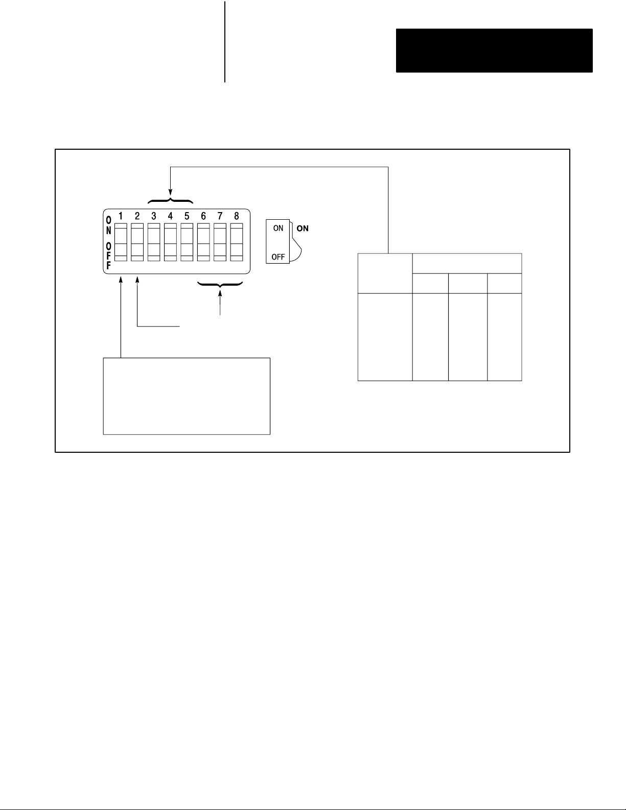
Figure 1.1
Message for Invalid Display of Processor Memory
ERR
113
][
14
11314
][
1.3
Additional Publications
1025
()
1770T3
Display (Actual content in processor memory)
1770T1 or T2 Display (Invalid display of processor memory)
ERR
16
02516
()
Additional information regarding PLC-2/30 programmable controller
components is available in:
PLC-2/20, PLC-2/30 Programmable Controller Assembly and
Installation Manual (publication 1772-6.6.2) contains necessary
information on installation, assembly, maintenance and troubleshooting.
Appendix C, Programming 0.01-Second Timers with the Mini-PLC-2
Programmable Controller.
15
Page 16

Chapter 1
Introduction
1.4
Terms Used in This Manual
We use the following terms to describe the various parts of your PLC-2/30
system.
Chassis — a hardware assembly used to house PC devices such as I/O
modules, adapter modules, processor modules, power supplies and some
processors (PLC-2/02, -2/16 and -2/17, for example).
I/O Group — The logical assignment of a specific input image table
word and its companion output image table word to a rack location. For
example: address 123 indicates an input module in rack 2, I/O group 3
This applies to all addressing modes.
Rack — an I/O addressing unit that corresponds to 8 input image table
words and 8 output image table words (128 input and 128 output
terminals).
Rack Fault — 1) The condition that occurs because of a loss of
communication between the processor and remote I/O chassis; 2) any
diagnostic indicator that lights up to signal a rack fault.
Slot — 1) The physical location where each module is placed within
a chassis; 2) a part of the Rack-Group-Slot addressing information for
intelligent I/O modules.
.
Slot Addressing — a method of assigning one input and one output image
table word to two slots, one slot, or one-half of a slot. (Appendix A is an
in-depth discussion on this topic.)
Slot Pair — two adjacent slots that can share image table words. Slot pairs
are: slots 0 and 1, 2 and 3, 4 and 5, and 6 and 7. (See Appendix A)
These and other terms are defined in Programmable Controller Terms
(publication no. PCGI–7.2).
16
Page 17

Chapter
Hardware Considerations
2
2.0
General
2.1
Select Switch
Mode
This chapter describes only those hardware items required when
programming or operating the PLC-2/30 programmable controller. For
more complete hardware information, refer to the PLC-2/20, PLC-2/30
Programmable Controller Assembly and Installation Manual (publication
no. 1772-6.6.2).
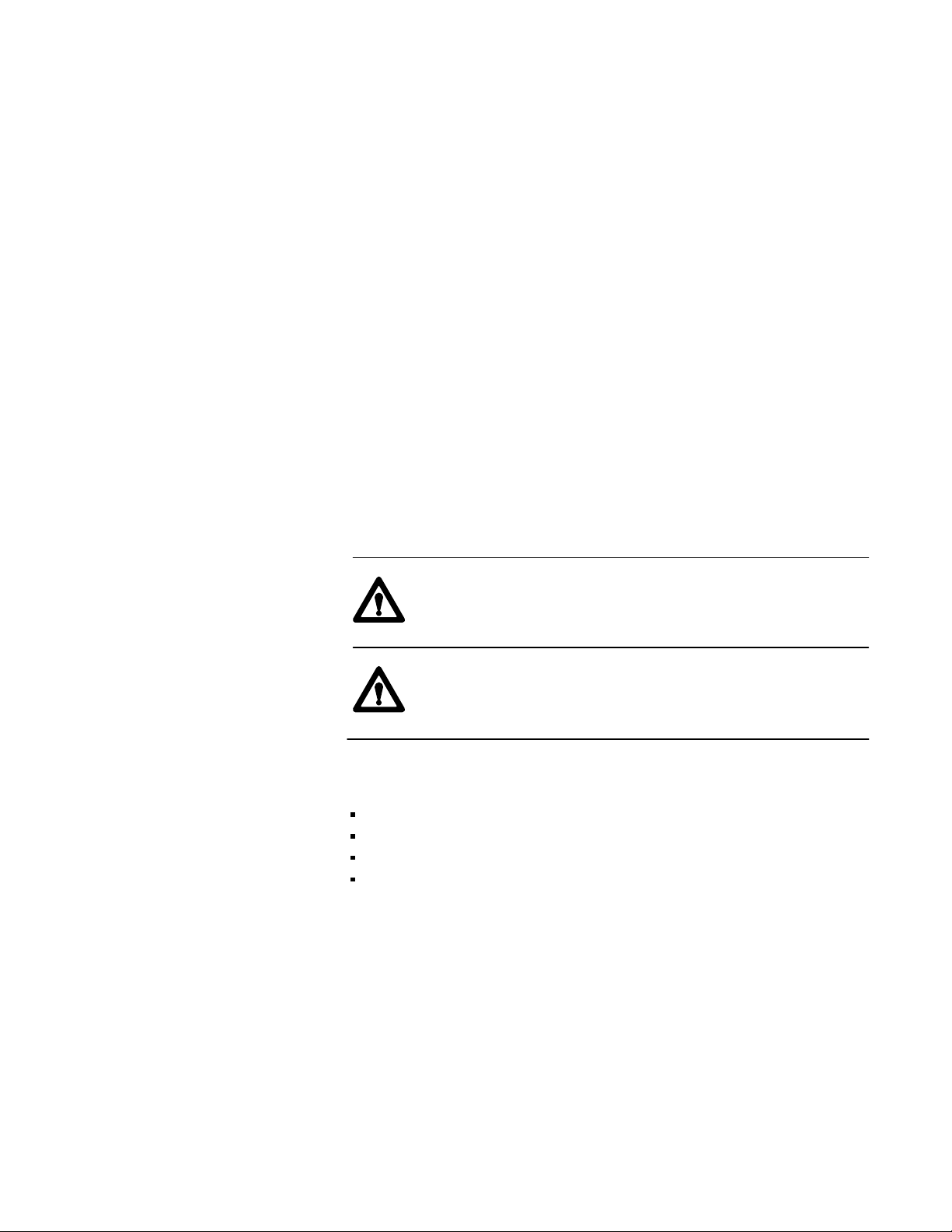
A four-position mode select switch (Figure 2.1) is located on the front of
the processor. You can select one of four positions with this switch:
PROG — This switch position places the processor in the program
mode. It is used when instructions are entered into memory. They can be
entered from an industrial terminal, a 1770-SA digital cassette recorder
or a 1770-SB data cartridge recorder. All outputs are disabled when the
switch is in this position.
TEST — This switch position places the processor in the test mode. The
user program is tested under simulated operating conditions without
actually energizing any output devices. All outputs are disabled in this
switch position.
RUN — This switch position places the processor in the run mode.
The user program will be executed and outputs are controlled by the
program. Changes to the user program or data table are not permitted in
this switch position.
RUN/PROG — This switch position places the processor in the
run/program mode. The processor functions as it does in the RUN
position. In this position, you can cause the processor to go into the
program or test mode without having to turn the switch to that position.
On-line changes to the program and/or data table are allowed in this
position with 1770-T3 or 1784-T50 industrial terminals.
The key can be removed from the processor in any of the four switch
positions.
21
Page 18
Chapter 2
Hardware Considerations
Diagnostic
Indicators
Figure 2.1
PLC2/30
Processor
Keylock
Mode
Select Switch
2.2
Memory
W
rite Protect
When the memory write protect jumper (Figure 2.2) is removed from a
1772-LH processor interface module, data table values can be changed
between word addresses 010
and 3778. These values can be changed only
8
when the processor is in the program mode or in the run/program mode
using on-line data change.
22
Page 19

Chapter 2
Hardware Considerations
Figure 2.2
Memory
W
rite Protect Jumper
HALFT
ONE WITH CALLOUT
2.3
RunTime
Errors
The remaining words in memory from 4008 to the end of memory,
including data table and user program, are protected and cannot be altered
by programming. The memory write protect feature guards against
unintentional changes to processor memory.
The processor and an industrial terminal can diagnose certain errors
occurring during the execution of the user program which result from
improper programming techniques. For example, it is possible to program
a series of instructions which require the processor to perform an operation
which it cannot do or perform an operation which is defined as illegal
(such as jump to a label that is not located closer to the end of program;
i.e., a jump backwards). These errors become apparent only while the
program is being executed, so are termed run-time errors. If a run-time
error occurs, the processor halts program execution and the PROCESSOR
FAULT indicator illuminates.
The first step in diagnosing run-time errors is to connect the industrial
terminal. It will display the message run-time error in the initial mode
select display. If the industrial terminal is already connected at the time
that a run-time error occurs, the ladder diagram is replaced by the mode
select display containing the error message. Run-time errors can be
detected by the industrial terminal when the processor is in either of two
23
Page 20

Chapter 2
Hardware Considerations
modes, program or remote program. (If the keyswitch is in
RUN/PROGRAM position, the industrial terminal automatically puts
the processor into remote program mode. If the keyswitch is in the RUN
position, or when it is connected to the processor through the 1771-KA2
communications adapter module, you must manually change the keyswitch
to the PROGRAM position).
WARNING: Forces are immediately removed if a Run-time
error occurs.
After returning the industrial terminal display to ladder diagram mode by
pressing [1][1] in mode selection operation, the industrial terminal displays
the instruction that caused the error with a message describing the run-time
error.
2.4
Processor Diagnostic
Indicators
After you have corrected the run-time error by editing the user program,
the processor can be restarted by switching to the run or run/program
mode.
Five indicators are located on the front of the processor (Figure 2.1). You
should become familiar with these indicators.
MEMORY FAULT — Illuminates when an error in the parity of data
retrieved from memory is detected. Changing the mode select switch to
the PROG position or cycling line power may clear this fault condition.
Reloading the program may also clear the fault.
BATTERY LOW — When the batteries for memory back-up are low,
this red indicator flashes on and off. Alkaline batteries will continue
to back up memory for about one week after the BATTERY LOW
indicator begins to flash. Lithium batteries have a longer life, but are
essentially dead when the indicator flashes. Regular replacement of
the batteries is recommended: for alkaline, every 6 to 12 months; for
lithium, every 2 years. (See the Assembly and Installation manual for
replacement details, publication no. 1772-6.6.2.)
The low battery bit, bit 027/00, will cycle on and off when a low battery
voltage condition is detected and the mode select switch is not in the
PROG position. Programming techniques can be used to examine this
bit and to control some type of alerting device when a low battery
condition exists.
24
Page 21

Chapter 2
Hardware Considerations
PROCESSOR FAULT — Illuminates when the logic circuits controlling
the processor scan fail or if processor error or run-time errors occur
which cause the processor to halt operation.
If the processor fault is a run-time error, the industrial terminal will
display RUN TIME ERROR when the keyswitch is in the PROGRAM
or RUN/PROGRAM position.
RUN — Illuminates when the processor is in the run or run/program
mode. It also indicates that outputs are being controlled by user
program.
DC ON — Illuminates when the 5.1V DC line to the logic circuitry in
the processor memory and I/O modules is satisfactory.
2.5
PowerUp
Recovery
2.6
Switch Group Assembly
When local I/O racks are powered by 1771-P3, -P4, -P5 or -P7 power
supplies, the processor control module (Cat. No. 1772-LG) may experience
a problem with these racks.
Upon recovery from a power lock (momentary or otherwise), processors in
the RUN or TEST mode attempt to read the local racks before the power
supplies are ready. This leads to a processor fault. The fault may be
identified by the conditions of the indicators:
Indicators
1772LG Module
Series A, Rev. L OFF ON
Series A, Rev. K or earlier OFF OFF
RUN
PROC FAULT
If the problem occurs, put the keyswitch in the program load position, then
return to RUN, or cycle power to the processor.
A switch group assembly is located on the I/O chassis backplane. It is used
to control output behavior when a fault occurs, to identify the I/O rack
number for local systems and to identify the addressing mode for remote
systems.
The switch and its functions, when used in local racks, are shown in
Figure 2.3. In this setup, the PLC-2/30 is communicating with the I/O
chassis through a 1771-AL Local I/O Adapter module.
25
Page 22

Chapter 2
Hardware Considerations
When using remote I/O (the 1772-SD2 scanner and the 1771-ASB remote
I/O Adapter), these switches will be set according to the adapter module’s
requirements.
2.6.1
Last State Switch
2.6.2
I/O Rack Number
The last state switch (switch no. 1) on the 1771 I/O chassis must be
properly set. ON indicates that the outputs are left in their last state when
a fault is detected. Machine operation can continue after fault detection.
OFF indicates that the outputs are de-energized when a fault is detected. In
addition, in remote systems, the switches on the 1772-SD2 Remote I/O
Scanner/Distribution panel and the 1771-ASB Remote I/O Adapter
must be properly set. Refer to publications 1772-2.18 and 1771-6.5.37,
respectively, for information on their switch settings.
WARNING: Switch No. 1 of the 1771 I/O chassis should be set
to OFF for most applications. This allows the processor to turn
controlled devices off when a fault is detected. If this switch is
set to ON, machine operation can continue after fault detection.
Damage to equipment and/or injury to personnel could result.
The setting of switches 3, 4 and 5 determines the I/O data table and
program address of the modules in this chassis — this is the local rack
number.
26
Improper setting of these switches will result in misdirected
communications between processor and the desired I/O rack.
Page 23
Chapter 2
Hardware Considerations
Figure 2.3
I/O Chassis Backplane Switch Settings for Local I/O Systems
1771
On:
Off:
2.7
Industrial Terminal
No significance should be set to OFF
Outputs remain in last state
when fault is detected.
Outputs deenergized when
fault is detected.
The 1770-T3 and 1784-T50 industrial terminals are the primary
programming terminals for the PLC-2/30 programmable controller. They
are used to load, edit, monitor and troubleshoot the user’s program in the
PLC-2/30 memory.
Local
Rack
Numbers
1
2
3
4
5
6
7
Switch
354
On
On
On
On
Off
Off
Off
On
On
Off
Off
On
On
Off
On
Off
On
Off
On
Off
On
2.8
Local System Structure
For detailed information about the 1770-T3 Industrial Terminal, refer to
the Industrial Terminal System User’s Manual, publication no. 1770-6.5.3.
For detailed information about the 1784-T50 Industrial Terminal, refer to
the Industrial Terminal T50 User’s Manual, publication no. 1784-6.5.1.
A local system has the processor and each I/O chassis within 3-6 cable feet
of each other. Up to 7 local I/O racks may be assigned.
For proper transmission of data between the PLC-2/30 processor and
local bulletin 1771 I/O modules, the I/O chassis must contain a local I/O
Adapter Module (Cat. No. 1771-AL). The local adapter module must be
installed in each I/O chassis used with the processor. Diagnostic indicators
27
Page 24

Chapter 2
Hardware Considerations
on the front panel of the local adapter module aid in troubleshooting. These
indicators are:
ACTIVE — Illuminates when proper communication is established
between the processor and the I/O chassis. It also indicates that DC
power is properly supplied to the I/O chassis. It is normally on.
RACK FAULT — Illuminates when I/O data is not in the proper format.
It is normally off.
Possible causes of a rack fault are:
Data parity error on address or control lines
Missing terminator plug
Disconnected/broken communications cable
No power at the processor.
An I/O Interconnect cable is required to connect between the PLC-2/30
and local I/O rack adapter modules. It is available in two sizes:
2.9
Remote System Structure
3 ft. I/O Interconnect cable (.92m) 1777–CA
6 ft. I/O Interconnect cable (1.85m) 1777-CB
I/O Cable Terminator Plug 1777-CP
(used to “close” the I/O interconnect cable link at the last I/O adapter
module)
A remote system allows the processor and the I/O chassis to be separated
by up to 10,000 cable feet (approx. 3,048 meters). Up to 7 remote I/O
racks may be assigned.
Proper transmission of data between the PLC-2/30 processor and
remote bulletin 1771 I/O modules requires a 1772-SD2 Remote I/O
Scanner/Distribution Panel plus a 1771-ASB Remote Adapter in each I/O
chassis. Connection between the PLC-2/30 processor and the 1772-SD2
is through a 1772-CS interconnect cable. Connection from the 1772-SD2
to a 1771-ASB Remote I/O Adapter and from one remote I/O adapter to
another is through 1770-CD twinaxial interconnect cable.
The front of the 1772-SD2 distribution panel has eight bicolor red/green
LED indicators. If the I/O chassis is used and serial communication is
valid, the RACK STATUS LED will be green. If the I/O chassis is not
used, the LED is off. For an I/O rack fault condition, the corresponding
RACK STATUS LED will be red. The rack 0 indicator will also go to red
if there is a dependent I/O fault.
28
Page 25

Chapter 2
Hardware Considerations
Three diagnostic indicators are located on the front of the 1771-ASB
adapter. These indicators are:
ACTIVE — Illuminates when proper communications have been
established between the 1772-SD2 distribution panel and the 1771-ASB
adapter, DC power is properly supplied to the I/O chassis and
1771-ASB adapter is actively controlling the I/O. The ACTIVE
indicator is normally on.
ADAPTER FAULT — Illuminates when the module is not operating
properly. It tells you that a fault has been detected and that the I/O
chassis has responded in the manner selected by the last state switch.
When this indicator is on, the other indicators are no longer valid. the
ADAPTER FAULT indicator is normally off.
I/O RACK FAULT — Illuminates when a fault has been detected at the
1771-ASB adapter, the I/O chassis, or the logic side of the I/O modules.
The I/O RACK FAULT is normally off.
2.10
Local/Remote
Structure
System
NOTE: For a full listing of the possible combinations of these
indicators (on, off or blinking), see the 1771-ASB User’s manual
(publication no. 1771-6.5.37).
A local/remote system has both nearby (3-6 cable-ft) and remote (up to
10,000 cable-ft) I/O chassis. Up to 2 local and 5 remote racks may be
assigned.
The PLC-2/30 processor system can also be configured with a combination
of local and remote I/O chassis. Each local chassis must have a 1771-AL
Local I/O Adapter module. And as previously stated, communication with
the remote chassis (one or more) requires a 1772-SD2 Remote Distribution
panel and one 1771-ASB Remote I/O Adapter in each chassis.
The 1772-SD2 distribution panel may be connected directly to the
processor interface module or up to two local I/O chassis may precede it.
Connection to the preceding local I/O chassis is made with a 1772-CS
interconnect cable.
NOTE: The 1772-SD2 must not be more than 10 cable feet from the
PLC-2/30 processor module.
29
Page 26

Chapter 2
Hardware Considerations
CAUTION: For proper system data communications, a
local/remote system structure with 2 local racks, you must use a
1777-CA cable (3 ft./.92m) between the processor and the two
local racks. You must also use the 1772-CS cable (3 ft./.92m)
from the second local rack to the distribution panel.
2.11
Hardware Addressing
Modes
2.12
Auxiliary Power Supplies
The term “addressing mode” refers to the method of hardware addressing
within individual I/O chassis. Appendix A, Hardware Addressing, provides
a complete presentation on 2-slot, 1-slot and 1/2-slot addressing. In
general:
Local I/O chassis that are communicating through a 1771-AL Local I/O
Adapter module can only be 2-slot addressed.
Remote I/O that are communicating through a 1771-ASB Series A
Remote I/O Adapter module can be addressed in either 2-slot or 1-slot
modes.
Remote I/O that are communicating through a 1771-ASB Series B
Remote I/O Adapter module can be addressed in either 2-slot, 1-slot or
1/2-slot modes.
NOTE: Processor-to-I/O chassis communication requires the setting of
I/O chassis backplane switches. See the 1771-ASB Remote I/O Adapter
manual (publication no. 1771-6.5.37) for this information.
The Series C programmable controller’s power supply provides 4 amperes
of current to power local I/O chassis or the 1772-SD2 distribution panel.
When the total output current required to power these modules exceeds the
supply, or a core memory is issued, an auxiliary power supply must be
used. The total output current must not exceed the rating of the auxiliary
power supply.
2.12.1
1771P2 Auxiliary Power
Supply
210
The 1771-P2 power supply provides 6.5 amperes to power one bulletin
1771 I/O chassis with a maximum 128 I/O. This includes the adapter and
the I/O modules in the chassis.
This power supply may be operated from either a 120 or a 220/240V AC
source.
Page 27

Chapter 2
Hardware Considerations
2.12.2
1777P2
Auxiliary Power
Supply
2.12.3
1771P3, P4, and P5 Slot
Power Supplies
The 1777-P2 Series C power supply provides 9 amperes to power one or
two bulletin 1771-I/O chassis. This includes the I/O adapter and the I/O
modules in each chassis. The power supply must be used to power the
1772-SD2 distribution panel when the PLC-2/30 processor contains a core
memory module.
This power supply may be operated from either a 120 or a 220/240V AC
source.
These power supply modules provide 5V DC for an I/O chassis. The -P3
and the -P4 operate on 120V AC; the -P5 operates on 240V DC. The -P3
supplies up to 3 amperes to an I/O chassis; the -P4 and -P5 supply up to 8
amperes to an I/O chassis.
You may place one of these modules in any slot of a Series B 1771
Universal I/O chassis except the adapter/processor slot. Follow the
recommendation of the Power Supply Considerations section of
publication no. 1771-2.111 when locating these modules in a
1771 Series B I/O chassis.
Full specifications are in publication no. 1771-2.111.
2.12.4
1771P7 Power Supply
2.12.5
1771PSC Power Supply
Chassis
The 1771-P7 power supply provides 16 amperes to power one bulletin
1771 I/O chassis. This includes the adapter and the I/O modules in the
chassis.
This power supply may be operated from either a 120 or a 220/240V AC
source.
NOTE: The 1771-P7 power supply may not be used in conjunction with a
slot power supply.
The 1771-PSC provides 4 slots for mounting modular power supplies to
provide up to 16 amperes to a 1771 Series B Universal I/O chassis. It can
also be used to mount communication modules that need only +5V DC and
a processor enable signal.
The power supply chassis may be mounted separately (when used with
communications modules) or mounted directly to 1771-A1B, A2B or A4B
I/O chassis (when supplying additional backplane current and/or when
supporting communications modules).
211
Page 28
Data Table
Chapter
3
3.0
General
3.1
Memory Structure
MSB LSB
This chapter introduces concepts and terminology necessary for a general
understanding of programmable controller memory. It explains the
memory organization of the PLC-2/30 programmable controller.
The memory of the processor can be thought of as a large arrangement of
storage points, each called a BInary digiT, or bit (Figure 3.1). A bit is the
smallest unit of information a memory is capable of retaining. Information
stored in each bit is represented as a 1 or 0. When a bit is on, it is
represented by a logic 1. When a bit is off, it is represented by a logic 0.
Figure 3.1
Memory
Upper Byte Lower Byte
17 16 15 14 13 12 11 10 07 06 05 04 03 02 01 00
1001110111000110001001011011100
W
ord Structure
1
Address 030
Word
W
ord Address 031
8
8
17 16 15 14 13 12 11 10 07 06 05 04 03 02 01 00
1001010110001000011110001001000
Each bit in a word is identified by a two-digit number using the octal
numbering system. Memory bits are numbered 00 through 07 and 10
through 17, with the least significant bit (LSB = 00
most significant bit (MSB = 17
) at the left.
8
A group of 8 bits forms a single byte. A byte is defined as the smallest
complete unit of information that can be transmitted to or from the
processor at a given time.
0
W
ord Address 1700
W
ord Address 1701
) at the right and the
8
8
8
31
Page 29

Chapter 3
Data Table
A group of 16 bits makes up a word. This word can be thought of as being
made up of two 8-bit bytes; a lower byte and an upper byte.
Because of its function in memory, one PLC-2/30 word may also be
thought of as a memory location: when a word is being used, an actual
physical location in memory is being accessed.
A specific bit in memory can be identified by combining the word address
and bit number to form the bit address, such as 030/12 or 1701/04. The bit
address is shown by writing the word address above the instruction and the
bit number below it.
3.2
Memory Organization
3.2.1
Data Table
The processor can have a memory capacity of up to 16,256 words. These
memory words are organized by their word address and are divided into
three major areas (Figure 3.2):
Data table
User program
-Main Program
-Subroutine Area
Message Storage Area
All input/output status and user program instructions are stored in one of
these parts (Figure 3.2).
Data table words, and/or the 16 bits in each word, are controlled and
utilized directly by the processor. The processor uses the status of input
devices and the control logic established in the user program to determine
the status of output devices. Transfer of input data from input devices and
transfer of output data to output devices occurs during the I/O scan. If
the output instruction’s status changed in the program, the actual output
device’s on/off status is updated during the I/O scan to reflect this change.
32
Page 30
Chapter 3
Data Table
Decimal
Words
Up to
16,256
Total
8
64
72
128
256
384
512
Figure 3.2
PLC2/30
Decimal
Words
Per Area
Processor W
8
Rack 1010017
Rack 2020027
Rack 3030037
Rack 4040047
Rack 5050057
Rack 6060067
56
8
56
128
128
128
4
128640
Rack 7070077
Processor W
Rack 11
Rack 2120127
Rack 3130137
Rack 4140147
Rack 5150157
Rack 6160167
Rack 7170177
T
imer/Counter ACC V
Internal Storage
T
imer/Counter Preset V
Internal Storage
User
(User Program Begins
After End of Last
Data T
End of Program
Message Storage
Memory Organization (Expanded Data T
ork Area
No. 1
1
ork Area
No. 2
10117
2
alues or
alues or
Expansion
1
Expansion
2
Expansion
3
(etc.)
Program Storage
able Expansion)
3
Octal
ord Address
W
000
007
010
77
100
107
110
177
200
277
300
377
400
577
600
777
1000
1177
1200
17777
able)
Output Image Table
Rack address areas that are
not configured as output image
table become available for
timer/counter accumulated
values or word/bit storage.
Input Image Table
Rack address areas that are
not configured as input image
table become available for
timer/counter preset values or
word/bit storage.
Data table can be expanded in
128 word increments (unused
sections are utilized for user
program storage) up to 8064
words maximum.
1
027 - Bits in this word are used by the
processor for battery low condition, message
generation, and data highway
output modules in rack 2, I/O group 7.
2
125 and 126 - These words are used to
indicate remote rack fault
I/O system. Do not put input modules in rack
2, I/O groups 5 or 6.
3
Report generation messages can be stored in
memory locations not used by data table or
user program.
4
Maximum data table size is 8192 words.
. Do not put
status
in a remote
33
Page 31

Chapter 3
Data Table
The first 128 words of the memory are set aside for data table storage.
This number includes 32 words for I/O image tables (i.e., 2 full racks),
16 words for processor work areas and 80 words for timers/counters. If
timers/counters are not required, you can reduce the data table to 48 words.
Expansion is in increments of two words until a table of 256 is reached,
and then in increments of 128 words. The data table can be adjusted to
accommodate the full I/O capacity of the PLC-2/30 processor.
NOTE: The data table expansion capability should be utilized practically.
The user should allow sufficient room for both data table and user
program.
When the data table is set to 256 words, up to 112 timer/counter
instructions can be programmed or 224 storage words are available. Users
can also tail or data table input/output capacity in increments of 128 I/O up
to 896 I/O.
The function of the data table may be explained in relation to inputs and
outputs. Discrete input and output modules cannot store information.
Discrete input and output modules cannot store information. They contain
interface circuits only. Input/output status information (on/off) is actually
stored in memory areas called I/O image tables. An image is defined as an
exact duplicate array of information, that is, the states stored in a different
medium.
Data Table Areas
The data table of the PLC-2/30 programmable controller can be divided
into six distinct areas, assuming default data table size has not been
changed (Figure 3.3). These areas are:
Processor work area 1
Output image table
Timer/counter accumulated values or bit/word storage
Processor work area 2
Input image table
Timer/counter preset values or bit/word storage
The data table area has a default size of 128 words and is configurable
from 48 up to 8,064 words (with 8K word memory) or 8,192 words (with
the 16K word memory). This area stores the information needed in the
execution of the user program, such as input and output device status,
3-digit numeric values, and the status of internal storage points.
34
Processor Work Areas 1 and 2
There are two processor work areas: processor work area no. 1 (addresses
000
to 0078) and processor work area no. 2 (addresses 1008 to 1078).
8
Page 32

Chapter 3
Data Table
These memory locations cannot be accessed by the user. Their word
addresses are not available for addressing of any kind. The processor uses
both areas for internal control functions.
Output Image Table
The primary function of the output image table is to control the status of
outputs wired to the output modules. If the output image table bit is on, its
corresponding output is on. If the bit is cleared to off, its corresponding
output is off. These bits are controlled by instructions in the user program.
The processor controls the status of bits in the output image table as it
generates output commands. Actual hardware outputs change state only if
corresponding output image table bits change state or if they are forced.
NOTE: PLC-2/30 output terminals can be forced on or off through the
industrial terminal. The output image table bits, corresponding to output
terminals which are forced, do not change state.
The output image table ordinarily begins with word 010
ends with word 027
. However, word 027 is reserved and output or block
8
and ordinarily
8
transfer modules must not be placed in rack 2, I/O group 7.
The output image table therefore contains 16 word addresses, or 256
bit addresses. Using the industrial terminal, the output image table can
be reduced to 8 word addresses (128 bit addresses), or increased from
16 word addresses to 56 (896 bit addresses). By changing memory
configuration to 896 I/O (seven 1771-A4B I/O chassis with 2-slot
addressing), the 896 bit addresses represent the maximum number of
discrete outputs the processor can control.
Each bit in the output image table may be associated with a hardware
terminal address, although this is not always the case, since a
corresponding output module may not actually be placed in this I/O rack
slot. If it is, however, the terminal address is the same as the bit address.
A secondary function of the output image table is to provide a storage area
for bits or words. Words and/or bits in the output image table not actually
used to store the on/off status of devices can be used for data storage.
NOTE: Although only 11 bits of word 027
are actually used as processor
8
control bits, the remaining bits must not be used since inadvertent
alteration of these bits could occur. The processor sets bit address 027/00
ON and OFF to indicate a low battery condition. This bit can be examined
by instructions in the user program. (See Section 2.4)
8
35
Page 33

Chapter 3
Data Table
CAUTION: Word 027 is reserved for processor use. Do not put
block transfer or output modules in rack 2, I/O group 7.
Timer/Counter Accumulated Values, Bit/Word Storage
This area of memory is used to store accumulated values of timer/counter
instructions. The area may also be used as storage for words and/or bits.
Word addresses 030
to 0778 bound this area when memory is configured
8
for 256 I/O (maximum) and 40 Timer/Counter Instructions (Figure 3.3).
NOTE: Each timer or counter used actually requires two words of data
table memory: one from the accumulated value area (030
other from the preset value area (130
to 1778).
8
to 0778) and the
8
Input Image Table
The input image table duplicates the status of the inputs wired to input
modules. If an input is on, its corresponding input image table bit is set
to on. If an input is off, its corresponding bit in memory is cleared to off.
These bits are monitored by instructions in the user program.
Input image table bits are updated each scan cycle to correspond to the
information supplied by input modules.
The input image table is bounded by word addresses 110
(Figure 3.3). This area contains 16 word addresses, or 256 bit addresses.
With the industrial terminal, the input image table can be reduced to 8
word addresses (128 bit addresses), or increased to 56 word addresses
(896 bit addresses). By changing memory configuration to 896 I/O (seven
1771-A4B I/O chassis), the 896 bit addresses represent the maximum
number of discrete inputs the processor can monitor.
to 127
8
8
36
In a local PLC-2/30 controller, the total bits used, which represent actual
hardware inputs and outputs together, cannot exceed 896 I/O. This number
represents the maximum I/O capability of the PLC-2/30 Programmable
Controller and is possible only when the system is programmed with the
1770-T3 or 1784-T50 industrial terminal.
Page 34

Chapter 3
Data Table
CAUTION: If a remote I/O configuration is being used, words
1258 and 1268 may be used to store remote I/O fault bits. If this
is the case, input modules must not be placed in these slots (rack
2, I/O groups 5 and 6): unexpected machine operation may
result.
37
Page 35

Chapter 3
Data Table
Total
Decimal
Words
8
24
Decimal
Words
Per Area
8
16
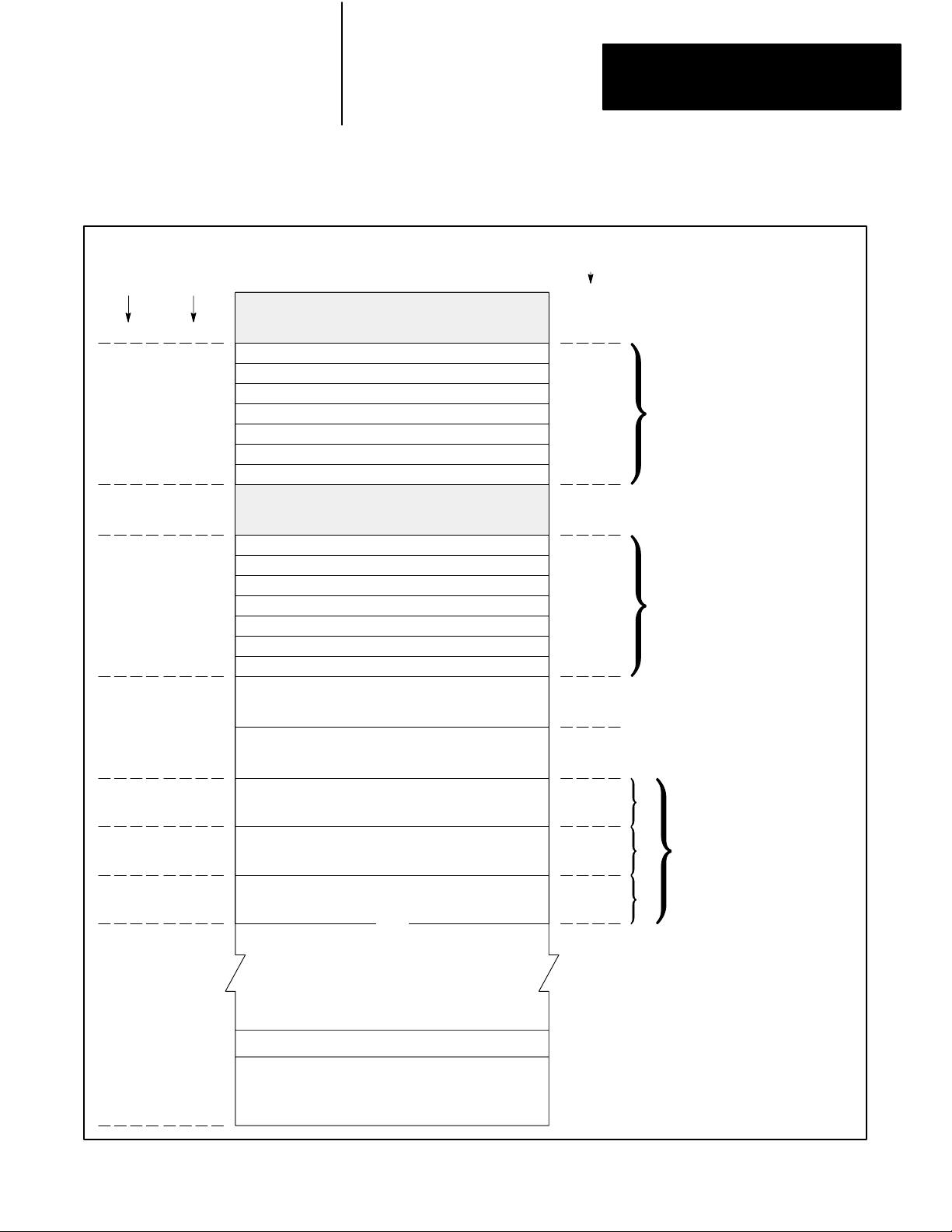
Figure 3.3
PLC2/30
Processor Work Area
Memory Organization (Default Configuration)
No. 1
Output
Image T
able
Octal
ord Address
W
000
007
010
026
027
030
Bit
Address
00
17
00
17
1
00
Up to
16,256
64
72
88
128
Timer/Counter
Accumulated V
40
Processor W
8
16
Preset V
40
alues (ACC)
Internal Storage
ork Area
No. 2
Input
Image T
able
Timer/Counter
alues (PR)
Internal Storage
User Program
17777
077
100
107
110
125
126
127
130
177
17
00
17
00
2
17
00
17
1
Bits in this word are used by the processor for
battery low condition, message generation,
and data highway. Do not put output modules
in rack 2, I/O group 7.
2
These words are used to indicate remote rack
fault status in a remote I/O system. Do not
put input modules in rack 2, I/O groups 5 or 6.
Default
Configured
Data T
able
(128 W
ords)
38
Page 36

Chapter 3
Data Table
Each bit in the input image table may have a corresponding real hardware
terminal on the I/O rack associated with it, although this may not always
be the case, since a corresponding input module may not actually be placed
in an I/O rack slot. If it does, the terminal address is the same as the bit
address. The correspondence between the two is illustrated in Figure 3.4.
CAUTION: Bit and/or word storage is not possible in the
input image table. Input bits which do not have an actual input
module in the I/O rack corresponding to address are cleared to
zero during each I/O scan.
39
Page 37

Chapter 3
Data Table
Input
Rack
Address
W
ord Address
Module
Group
Output
Image
Word
Input
Image
Word
Terminal
Figure 3.4
Relation
of Word Address to Hardware
Unassigned: Available
as Storage Bit
17 16 15 14 13 12 11 10 07 06 05 04 03 02 01 00
17 16 15 14 13 12 11 10 07 06 05 04 03 02 01 00
Assigned to an Input
Module T
erminal
Rack 1
I/O Group 1
010
010
01234567
32 I/O (1771A1B)
64 I/O (1771A2B)
96 I/O (1771A3B)
128 I/O (1771A4B)
310
Page 38

Chapter 3
Data Table
Timer/Counter Preset Values, Bit/Word Storage
This area of memory is used to store preset values of timer/counter
instructions. The area may also be used as storage for words and/or bits.
Word addresses 130
to 1778 bound this area when memory is configured
8
for 256 I/O (maximum) and 40 Timer/Counter Instructions (Figure 3.3).
NOTE: Each timer or counter used actually requires two words of data
table memory: one from the accumulated value area (030
other from the preset value area (130
to 1778).
8
to 0778) and the
8
Developing the Data Table
The data table configurations shown in Figure 3.2 should be used as a
guide when developing the data table. Determining the number of words
needed and assigning addresses is a procedure that requires care and
attention to detail. The data table should be roughed out in advance but
formally developed as you write your program. Data table documentation
forms, described in Section 3.4 and presented at the end of this section, or
their equivalent, should be used to keep track of each assigned data table
word and bit address.
Displaying the Data Table
To see the present configuration of the data table, press [SEARCH] [5] [4].
This action displays a diagram of the areas of memory including the data
table, user program, message area and the unused memory. The number of
words in each area is indicated in decimal.
To terminate this display, Press [CANCEL COMMAND] (Table 3.A).
311
Page 39

Chapter 3
Data Table
Table 3.A
Table Configuration
Data
Function Mode Key Sequence Description
Data Table Configuration Program
Program
Processor Memory Layout Any
Any
1
Requires Series B/Revision F (or later) keyboard.
[SEARCH]
[5][0]
[Numbers]
[SEARCH]
[5][0]
[RECORD]
[CANCEL
COMMAND]
[SEARCH]
[5][4]
[SEARCH]
[5][4]
[RECORD]
[CANCEL
COMMAND]
1
1
If the number of 128word sections is 1 or 2, enter this number,
the number of I/O racks, and the number of timers/counters. If
the number of 128word sections is 3 or greater, enter only this
number and the number of I/O racks. The industrial terminal
will calculate and display the data table size in decimal.
Prints first 20 lines of data table configuration.
To terminate.
Displays the number of words in the data table area, user
program area, message area, and unused memory.
Prints first 20 lines of memory layout display.
Data Table Area Configuration
The data table is factory-configured for 128 words (Figure 3.2). The data
table size can be decreased to 48 words or expanded to 8,064 words (with
8K memory) or 8,192 words (with 16K memory). Expanding the data table
provides additional timers/counters and space for files.
312
NOTE: In expanded areas, care must be taken to prevent files from writing
over timer/counter preset values or your program. We recommend that
you program all timers/counters in the first expanded areas and that you
program files after them in a separate expanded area.
Configuring The Data Table
You must configure the final data table size in processor memory before
entering your program. This is done by entering the number of 128-word
data table sections and, if necessary, the number of equivalent timers and
counters.
Page 40

Chapter 3
Data Table
After you have determined the layout of the data table, press [SEARCH]
[5] [0]. The following display appears:
NUMBER OF 128-WORD DATA TABLE SECTIONS
NUMBER OF I/O RACKS
NUMBER OF TIMERS/COUNTERS (IF APPLICABLE)
DATA TABLE SIZE
The number of 128-word data table sections, the number of I/O racks
(1-7), and the number of timers/counters (if applicable) to be entered is
prompted by a reverse-video cursor. The factory configuration for the data
table is one 128-word section, 2 I/O racks and 40 timers/counters.
The address of the last word in your data table determines the number of
128-word data table sections you will enter.
After planning and writing your program and logging all addresses on
data table assignment sheets, if the last address is at or less than 377
(256 words), the number of equivalent timers and counters must be
calculated. (Equivalent timers and counters includes internal storage
words, such as bit/word storage, files, and sequencer tables.) The
calculation is made using the following formula:
8
ET=T + C + IS/2
where:
ET = number of equivalent timers and counters
T = number of timers
C = number of counters
IS = number of internal storage words
When you have one 128-word data table block, you can specify as many
as 40 timers/counters. Should you need more than 40 timers/counters,
the processor will automatically increase the data table size by two
words for each timer or counter you add. The data table can be reduced
in 2-word decrements to a minimum of 48 words if 1 rack and 8
timers/counters are selected.
Or:
If the last data table word is at an address greater than 3778,
count the total number of 128-word data table sections used (the first
128-word section includes the I/O image tables). Count partially used
sections as complete sections.
When you enter 3 or more 128-word data table sections, the number
of timers and counters is included in the number of data table sections
entered. Therefore, the number of timers and counters need not be entered
and the industrial terminal will display N/A.
313
Page 41

Chapter 3
Data Table
After the number of I/O racks is selected, the industrial terminal will
compute and enter the data table size.
Anytime you reduce the size of the data table, the processor searches
for instructions in those areas. If an instruction exists in an area to be
deleted, the change will not be allowed and the following message will be
displayed: “INSTRUCTION EXISTS IN DELETED AREA.” To display
the rung that is preventing the change, press [SEARCH]. At that time, the
decision can be made whether to keep or delete the instruction.
Anytime you increase the size of the data table, the user program is
automatically moved into higher word addresses. However, once the
memory is full, expansion is not permitted and the message “MEMORY
FULL” is displayed. Press [CANCEL COMMAND] to terminate the data
table configuration display (Table 3.A).
Changing Data Table Areas
You may reduce data table size from the standard or default value of 128
words to 48 words when 8 timers/counters and one I/O rack are being
used. This assumes 8 words are reserved in both the input and the output
image table. Additional space is then made available for user program
instructions. Reductions can be made in decrements as small as two words
(one timer/counter). If the memory locations are occupied, the attempted
reduction fails.
You can increase data table size from 128 to 256 words, also in increments
of two words (one timer/counter). This provides up to 104 timers/counters
with 16 words reserved for each input/output image table. Above 256,
data table size is increased in sections of 128 words. You therefore gain the
use of an additional 128 words (64 timer/counter instruction addresses or
128 words for bit/word or file storage, or a combination of both) for each
expansion.
The processor determines whether sufficient unused memory remains for
the corresponding shifting of user program instructions from the area to be
addressed by the additional address area. If sufficient memory exists, the
required number of words are than reserved.
314
Input/Output Image Table Sizes
You may optionally alter the number of words reserved for input/output
image tables. Memory can be changed from 128 to 896 I/O, in increments
of 128 I/O (i.e., 1 rack).
By reducing memory areas required for inputs/outputs from 256 to 128
(from 2 racks to 1 rack), data table size remains unchanged, but an
Page 42

Chapter 3
Data Table
additional 7 timer/counter instructions become available. The previous
output image table addresses 020
accumulated values; previous input image table addresses 120
-0268 are now reserved for timer/counter
8
-1268, for
8
timer/counter preset values.
When I/O requirements are increased from the standard value of 256 to
384 (or from 2 racks to 3 racks), data table size does not change. Instead,
timer/counter areas (in the default memory configuration) are each
reduced by 8 words. Previous timer/counter accumulated value addresses
030
-0378 are now reserved for output image table; previous timer/counter
8
preset value addresses 1308-1378, for input image table.
When I/O image table size is increased from 384 to 512 (i.e., increase
from 3 to 4 racks), timer/counter areas are reduced by another 8 words.
Previous timer/counter accumulated value addresses 040
-0478 are
8
reserved for output image table. Previous timer/counter preset value
addresses 1408-1478 are reserved for the input image table. This same
progression continues, as follows:
when you increase the I/O to 640 (5 racks), accumulated address limits
become 060
to 0778 and the preset address limits become 1608 to 1778.
8
when you increase the I/O to 768 (6 racks), accumulated address limits
are 070
to 0778 and preset address limits are 1708 to 177
8
8
and with the maximum I/O increase to 896 (racks), accumulated address
limits and preset address limits are completely gone from the default
data table.
Data table expansion becomes necessary if 7 racks are selected and timers
or counters are desired. The first address available for accumulated storage
would be 200
and the first preset address would be 3008.
8
NOTE: Block transfer counter addresses must start immediately following
the I/O address. Therefore, if the I/O image table size is changed, the block
transfer instructions must be reprogrammed.
Memory Write Protect
In the processor, the inhibit feature is active when the user removes a
jumper from the 1772-LH interface module. This prohibits alteration of the
user program in any processor mode. The alteration of data table words
4008 and above is also prohibited except through the user program. Only
data table values between word addresses 010
either in run/prog or prog modes.
and 3778 can be changed
8
315
Page 43

Chapter 3
Data Table
3.2.2
User Program
You program is a group of ladder diagram instructions used to control an
application. It is initially entered into memory using an industrial terminal.
Main Program
The main program follows the data table in memory and stores all the user
program instructions that make up the ladder diagram program. Most
instructions are stored in one memory word. Some advanced instructions
require up to 8 memory words. Unless specified elsewhere, instructions
require one word of user memory when the address is 377
two words of user memory when the address is 400
8
Assuming that the data table size has not been changed from
factory-configured values, the user program begins after word address
177
.
8
In certain applications, this area of memory can further be divided into data
highway instructions, main ladder diagram program and subroutine area.
Some of the simple program instructions, such as Examine On, use one
word of memory. Others, such as file instructions, are more complex and
can use two or more words of user program memory. As the user program
is entered from the industrial terminal, the number of words is indicated at
the right of the END statement (including data table words). The words
remaining in memory can be determined by subtracting that number from
the total memory available.
or below and
8
or above.
316
Subroutine Area
The Subroutine area contains instructions of special or often repeated
sections of program. Its upper boundary serves as the END of program
statement for the main program.
The Jump-to-Subroutine (JSR) instruction is an output instruction that
enables you to jump to a defined ladder diagram subroutine when desired.
You use subroutines to optimize program scantimes.
By pressing the SBR key on the -T3 industrial terminal, you define the
beginning of the Subroutine area. This may not be removed once inserted
except by clearing memory. The Subroutine area is not scanned unless a
JSR has been energized.
Page 44

Chapter 3
Data Table
3.2.3
Message Storage Area
The message storage area begins after the END of user program statement
and it stores the alphanumeric characters of the messages.
The memory is capable of storing user-programmed messages for
hardcopy printout by compatible RS-232C data terminals. As many as 70
messages of varying length can be stored (198 messages can be stored
when using the 1770-RG Report Generation module).
Message storage immediately follows the END (of program) statement,
and is limited only by the number of unused words remaining in memory.
Each word remaining after the END statement is capable of storing 2
ASCII message characters. (Characters are defined as keyboard entries
made on the data terminal, such as A, 1, M, ., 8, space, etc.)
Messages are stored in numerical order. Messages 1 through 6 are
controlled by word 0278 and have the highest priority. The next 8
messages are controlled by the first user-designated message control word,
the next 8 in the second control word, etc. Eight consecutive words can be
reserved as message control words. (When using the 1770-RG module, 24
consecutive words can be reserved.)
WARNING: Bit addresses 02710
in the upper byte of the message control words may be used for
automatic report generation functions. Since the user program
examines these bits to determine report generation status
and may also set them to initiate various report generation
operations, these bits should not be used for other functions.
These words should also be reserved.
thru 027178 and all the bits
8
3.3
Hardware/Program Interface
3.3.1
Image Tables
It is important to understand how machine data, sensed by the input
modules, is used by the processor to turn output devices on or off. The
hardware-program interface occurs in the input/output image tables.
The primary purpose of the input image table is to duplicate the status (on
or off) of the input devices wired to input module terminals. If an input
device is on (closed), its corresponding input image table bit is on (1).
If an input is off (open), its corresponding input image table bit is off (0).
Input image table bits are monitored by user program instructions but are
controlled by the input devices.
The primary purpose of the output image table is to control the status (on
or off) of the output devices wired to output module terminals. If an output
image table bit is on (1), its corresponding output device is on (energized).
317
Page 45

Chapter 3
Data Table
If a bit is off (0), its corresponding output device is off (de-energized).
Output image table bits are controlled by user program instructions.
3.3.2
Instruction Address
Instruction addresses in the input/output (I/O) image tables take the form
of Figure 3.5. These addresses have a dual role. Each 5-digit address
corresponds (1) to an input or output table word (address) and (2) to a
hardware location.
Figure 3.5 shows how the 5-digit address corresponds to an input or output
table word. The first 3 digits define the function and logical address of a
single, 16-bit input or output image table word. The remaining two digits
represent a specific bit in that I/O table word.
Figure 3.6 shows how the 5-digit address corresponds to an input or output
module terminal. Using the same 010/12 address, the first 3 digits again
define the logical function and address of a specific I/O group. The
remaining two digits represent a specific input or output terminal in that
I/O group.
NOTE: See Appendix A, Hardware Addressing, for a complete
presentation on the relationship between specified hardware terminals and
their I/O image table addresses.
318
Page 46

Chapter 3
Data Table
Figure 3.5
Instruction
Address T
erminology
Concept Example
Hardware Terminology Hardware Terminology
Input
Word
Address
Bit
Address
(1) or Output (0)
Rack No. (17)
I/O Group No.
(07)
erminal No.
T
(0007, 1017)
Word
Address
Bit
Address
Output:
0
Rack No.: 1
I/O Group No.: 0
T
erminal No.: 12
Data Table Terminology Instruction Address
319
Page 47

Chapter 3
Data Table
Figure 3.6
Address to Hardware Relationship (2slot Addressing)
Bit
Bit
Outout = 0
Input = 1
Rack
Number
Left
Slot
0
Module
Group
Right
Slot
1
17 16 15 14 13 12 11 10 07 06 05 04 03 02 01 00
Upper Byte Lower Byte
Terminal
Rack 1
I/O Group 1
01234567
Word
Address
010
320
32 I/O
64 I/O
96 I/O
128 I/O
Page 48

Chapter 3
Data Table
3.3.3
Fundamental Operation
The hardware-program interface is illustrated in Figure 3.7 by showing
the operational relationship between the input and output devices, the
input/output image table and the user program.
When an input device connected to terminal 113/12 is closed, the input
module circuitry senses a voltage. The On condition is reflected in the
input image table bit 113/12. During the program scan, the processor
examines bit 113/12 for an On (1) condition. If the bit is On (1), the
Examine On instruction is logically true. A true condition is displayed as
an intensified instruction. A path of logic continuity is established and
causes the rung to be true. The processor then sets output image table bit
012/06 to On (1). The processor turns on terminal 012/06 during the next
I/O scan and the output device wired to this terminal becomes energized.
When the rung condition is true, the output instruction is intensified.
321
Page 49

Chapter 3
Data Table
Input T
113/12
2-Digit Bit and
T
erminal Address
Input Module in
I/O Rack No. 1,
I/O Group No. 3
erminal
Figure 3.7
Relationship
17 16 15 14 13 12 11 10 07 06 05 04 03 02 01 00
1 = ON
0 = OFF
100101
11110
BIT 012/06
of Word Address to Hardware
Output Image T
Input Image T
able
able
BIT 113/12
10001011110000
3Digit
Word Addresses
00100
1
0
010
012
017
110
113
Output Module in
Assigned I/O Rack No. 1,
I/O Group No. 2
8
8
8
8
8
Output T
012/06
Energized
Output
erminal
322
Closed
Input
113
1 = ON
0 = OFF
177
8
UserProgrammed Rung
012
( )| |
0612
Instruction
Intensified
When Enabled
When the input device wired to terminal 113/12 opens, the input module
senses no voltage. The Off condition is reflected in the input image table
bit 113/12. During the program scan, the processor examines bit 113/12
for an On (1) condition. Since the bit is off (0), logic continuity is not
established, the rung is false and the output instruction is not intensified.
The processor then sets output image table bit 012/06 to off (0). In the next
I/O scan, it turns off terminal 012/06 and the output device wired to this
terminal is turned off.
Page 50

Chapter 3
Data Table
3.4
Data Table Documentation
Forms
3.4.1
Data T
able W
ord Map
(1024 Word)
As you program your application, you should carefully record the
data table addresses of the program elements. The importance of this
documentation cannot be overemphasized. You will find it invaluable for
avoiding improper use of data table areas and as an aid in troubleshooting
and making program changes.
The data table documentation forms presented at the end of this chapter
can be reproduced or revised as needed. They include two general types:
Data Table Word Map (1024 word) and Data Table Map (128 word)
Data Table Word Assignments (64 word), Data Table Bit Assignments,
and Sequencer Table Bit Assignments
An example showing how the forms are used accompanies the
descriptions.
This form can be used to map the addresses of group data table words and
to concisely describe the function of each group. The groups can include
I/O Image Tables, Block Transfer, Timer/Counter, File and Sequencer
Instructions, Files and Sequencer tables.
The form has prenumbered rows representing addresses from 000
Each row has 32 spaces where each space represents one word address.
Any group of related word addresses can be designated on the map by
labeling or color coding the spaces representing their addresses. For
example, Figure 3.8 shows a completed portion of the data table word map.
The Timer/Counter Accumulated values are labeled in the spaces defined
by word address 040
labeled.
through 0718. Other data table areas are similarly
8
-7778.
8
323
Page 51

Chapter 3
Data Table
3.4.2
Data T
WORD
ADDRESS
000
040
100
140
200
240
300
able Map (128 W
Figure 3.8
Outputs
of Data T
Example
FROM (32
able W
Storage Storage Block
Timer/Counter
Not
Used
Inputs Storage
Timer/Counter
Files
This form can be used to log the bit status of a word and to describe the
ord)
function of groups of related words within a 128–word data table section.
In particular, it can be used to log initial conditions of files such as those
used for recipes, and to log assigned storage bits.
ord Map
WORDS)
Xfer
AC V
alues Storage
Block Xfer
PR V
alues Storage
TO
WORD
ADDRESS
037
077
137
177
237
277
The lower two digits of the 3-, 4- or 5-digit word address are prenumbered
in the left-hand column. The bit numbers, 00-17, complete the 5-, 6- or
7-digit bit address. The starting word address can be written once for the
entire 64-word column.
For example, Figure 3.9 shows a completed portion of the data table map.
The left-hand column represents the addresses 200/00 through 277/17
because a 2 is written in the starting word address box at the top of the
column. Two 4-word files are illustrated. The data of the File-to-File move
instruction, FFM062, is entered in binary. The data of the File-to-File
move instruction, FFM063, is entered in hex.
324
Page 52

Chapter 3
Data Table
17 1007 00
00
2
01
36
37
0110101101101111
40
0010100111010001
41
0101110100101010
42
1010101001010100
43
44
45
46
47
50
51
Figure 3.9
Example
of Data T
able Map
STARTING WORD ADDRESS
2
00
BIT NUMBER
AC3B
24F8
C3D5
5B4E
DESCRIPTION
FFM 062
(Binary)
FFM 063
(Hex)
3.4.3
Data T
able W
ord
Assignments (64 Word)
This form can be used to write functional descriptions of word addresses
used in the data table for word storage, timers and counters, etc.
The form is divided into two 32-word columns. The words can be
numbered consecutively through the entire 64 words. Or, the right-hand
column can be numbered 1008 greater than the left-hand column to
conveniently track accumulated and preset values. In either case, the
lowest digit of the 3-, 4- or 5-digit word address is prenumbered, 0-7.
For example, a portion of the data table word assignment sheet is shown
in Figure 3.10. It illustrates timer and counter functional descriptions for
accumulated values starting at word address 200
at 300
address boxes, respectively.
. A 20 and 30 were written into the left-hand and right-hand word
8
and preset values starting
8
325
Page 53

Chapter 3
Data Table
ADDR
WORD
0
20 Master
1
2
5
6
7
cycle time, AC
Drillhead #1, dwell time, AC
No. of passes, AC
No. of reject parts, AC
3.4.4
Data Table Bit Assignments
Figure 3.10
Example
DESCRIPTION
of Data T
able W
ord Assignments
WORD ADDR
0
30
Master cycle time, PR
1
Drillhead #1, dwell time, PR
4
5
No. of passes, PR
6
No. of reject parts, PR
DESCRIPTION
This form can be used to log the function of input, output and storage bits.
Similar to the word assignment sheet, the bit assignment sheet is divided
into two 2-word columns. The words can be numbered consecutively, or
the right-hand column can be numbered 1008 greater than the left-hand
column for the convenient logging of input, output and/or storage bits
having the same I/O group number. The bit numbers are prenumbered,
00-17.
WORD BIT
0
012 112CR1, run auto (sto.)
0
0
1
CR2, part preset latch (sto.)
0
2
CR3, op. compl. (sto.)
0
3
DESCRIPTION
For example, a portion of the data table bit assignment sheet is shown
in Figure 3.11. It illustrates logging the input devices associated with
I/O group 2 and the storage of the corresponding storage word 012
(complement of word 112). Word address 012 and 112 have been entered
into corresponding word address boxes in the left- and right-hand columns,
respectively. The 3-, 4- or 5-digit word address is entered once for all 16
bits.
Figure 3.11
Example
of Data T
able Bit Assignments
WORD BIT
0
0
0
DESCRIPTION
0
LS1 Forward overtravel
1
PRS1 Part detect
2
PB1 Up-jog
326
Page 54

Chapter 3
Data Table
3.4.5
Sequencer Table Bit
Assignments
This form can be used for any one of the three Sequencer instructions to
log the data associated with each step.
This information added to the heading of the assignment sheet should be
identical to the information displayed in the data monitor mode heading
and in the ladder diagram mode instruction block of the sequencer
instruction. The mask row is used to log mask data, if required. The
remaining rows are for logging the data of each step. The data can be
logged in binary or in hex. The step numbers should be written in the
left-hand blank column. The from-to addresses at the bottom of the sheet
are the starting and ending file addresses for each column of the sequencer
tables.
For example, Figure 3.12 shows a completed portion of a sequencer table
bit assignment sheet for an 8-step, 3-word-wide sequencer input
instruction. The mask and steps 1 and 2 have been completed in binary.
Steps 3-8 have been completed in hex for the sake of illustration. The
starting and ending word addresses of each column of the sequencer table,
400 to 407, 410 to 417, and 420 to 427, respectively, have been entered at
the bottom of each column.
327
Page 55

Chapter 3
Data Table
Figure 3.12
Example
SEQUENCER
COUNTER
WORD ADDR:
MASK ADDR:
D
E
V
I
C
E
MASK
STEP
FROM ADDR
ADDR:
WORD #1 WORD #2 WORD #3 WORD #4
17 1007 00
N
A
M
E
//// /// ///////////// /// ///////////// /// /////0000
1010 011 0101010101010 011 0101010101010 011 010101010
1
0010 100 0100100101010 011 0101010101010 011 010101010
2
ABF8EA4CA3D9
3
3C4D2812B5F4
4
1DC134D2
CFF265ECH127F
6
47D239B1ABC6
7
B3F823FE1C2A
A
TO ADDR
204 400 427
112 113 114
403 431 432
17 1007 00 17 1007 00 17 1007 00
400 410 420
407 417 427
of Sequencer Table Bit Assignments
Input
FILE
to
CD461
1
SEQ LENGTH
3.4.6
I/O Assignments
328
Once the rough sketch of the application is complete, the programmer can
assign data table bit addresses to the input and output devices wired to the
controller. The 5-digit bit address directly corresponds to the location of
each I/O device with respect to the rack number, I/O group and terminal
number. Because the bit address is hardware-related, the programmer
cannot arbitrarily assign bit addresses to I/O devices. Refer to Section
3.2 on memory organization. Analog modules and other intelligent I/O
modules use word addresses rather than 5-digit bit addresses. Refer to the
user’s manual for each module for more information on addressing and
wiring.
The installer and programmer of the PLC-2/30 Programmable Controller
should work together to determine the best placement of the I/O modules
within the I/O chassis. To simplify installation and troubleshooting
procedures, it may be desirable to group like modules together. It is also
helpful to document I/O assignments on a form such as the form presented
at the end of this section. Recommendations for I/O wiring and module
Page 56

Chapter 3
Data Table
placement can be found in the PLC-2/20, PLC-2/30 Programmable
Controller Assembly and Installation Manual (publication no. 1772-6.6.2).
3.4.7
Timer/Counter Assignments
In addition to I/O assignments, timers and counters must also be assigned
data table word addresses. It is best to make a list of the word addresses
used for timers and counters on data table documentation forms. Later,
when sizing the data table, this list will be useful.
The first available timer/counter address depends on the number of I/O
racks used. The PLC-2/30 Processor (Cat. No. 1772-LP3) can have up to 7
I/O racks. The corresponding addresses for the first timer/counter locations
are shown in Table 3.B. If block transfer is to be used, each block transfer
instruction requires one T/C address pair as its data address. The first
available location must be reserved for block transfer (Chapter 10).
Table 3.B
Timer/Counter
# I/O Racks First Timer/Counter Word Address
1
2
3
4
5
6
7
Address for 1772LP3
020
030
040
050
060
070
200
3.4.8
Data Storage Assignments
Data storage has two categories. They are:
Bit/Word storage
File storage
Bit/Word Storage
Bit/word storage addresses can be located in all unused areas of the data
table excluding the input image table and processor work areas. Data table
addresses for bit and word storage should be chosen carefully to optimize
memory use.
The following recommendations for bit and word storage should be
considered:
Unused data table words in T/C areas can be used for bit/word storage.
To conserve memory, use both the accumulated and preset value words
for storage.
329
Page 57

Chapter 3
Data Table
Output image table words can be used for storage when the
corresponding input image table words are used for nonblock transfer
input modules. However, when there is a vacant I/O group or slot in the
I/O chassis, do not use image table words for storage. This will allow
room for future system expansion.
Bits 14-17 of a timer or counter preset word can be used for bit storage,
provided data is not transferred to the preset word by a Get/Put transfer
or the timer is not set for a 0.01 time base.
Unused input image table words should not be used for storage. They
are cleared to zero during each I/O scan.
Word 027 should not be used for storage. Many of the bits are used by
the processor for control functions.
File Storage
Files are located in consecutive word addresses in the data table. Usually
file storage should be immediately below the last timer/counter preset
address. Files can include their own unique addresses as well as duplicate
preassigned addresses. Therefore, files should be carefully entered on data
table documentation forms.
Sequencer tables, as with files, should be entered on the data table
documentation forms because they also may have their own unique
addresses and/or duplicate preassigned addresses. Moreover, sequencer
tables can be 1, 2, 3, or 4 words wide. This means that the number of steps
in a sequencer table must be multiplied by the number of words wide
(words per step) in order to obtain the total number of consecutive data
table words required by a sequencer table.
The following recommendations should be considered:
Do not inadvertently allow files to overlap other files or a data table
boundary.
Leave space for file growth. If addresses between files are used for
bit/word storage, the addresses can be easily reassigned elsewhere if the
need arises.
330
Page 58

PROJECT NAME
Data Table
Chapter 3
ALLEN-BRADLEY
Connection Diagram Addressing
BULLETIN 1771 I/O Chassis
(8-point Modules)
PAGE
DATE
DESIGNER
331
OF
Page 59

332
ÍÍ
Bulletin 1771 I/O Chassis
CONNECTION DIAGRAM ADDRESSING WORKSHEET
Data Table
Chapter 3
PROJECT NAME
(16-point Modules)
PAGE
DATE
DESIGNER
OF
Page 60

PROJECT
NAME
ALLEN-BRADLEY
Programmable Controller
DATA TABLE WORD MAP
(1024 WORD)
PROCESSOR
Chapter 3
Data Table
PAGE OF
ADDRESS TO
DESIGNER
WORD
ADDRESS
000
040
100
140
200
240
300
340
400
440
500
540
600
640
700
740
000
040
100
140
200
240
300
340
400
440
500
540
600
640
700
740
FROM
(32 WORDS)
DATA TABLE SIZE
TO
WORD
ADDRESS
037
077
137
177
237
277
337
377
437
477
537
577
637
677
737
777
037
077
137
177
237
277
337
377
437
477
537
577
637
677
737
777
REF
333
Page 61

Chapter 3
Data Table
PROJECT
NAME
ALLEN-BRADLEY
Programmable Controller
DATA TABLE WORD MAP
(128 WORD)
PROCESSOR
PAGE OF
ADDRESS TO
334
DESIGNER
STAR
TING WORD ADDRESS
00 00
BIT NUMBER
17 10 07 00
00
01
02
03
04
05
06
07
10
11
12
13
14
15
16
17
20
21
22
23
24
25
26
27
30
31
32
33
34
35
36
37
40
41
42
43
44
45
46
47
50
51
52
53
54
55
56
57
60
61
62
63
64
65
66
67
70
71
72
73
74
75
76
77
DESCRIPTION
DATA TABLE SIZE
STAR
TING WORD ADDRESS
BIT NUMBER
17 10 07 00
00
01
02
03
04
05
06
07
10
11
12
13
14
15
16
17
20
21
22
23
24
25
26
27
30
31
32
33
34
35
36
37
40
41
42
43
44
45
46
47
50
51
52
53
54
55
56
57
60
61
62
63
64
65
66
67
70
71
72
73
74
75
76
77
DESCRIPTION
Page 62

ALLEN-BRADLEY
Programmable Controller
DATA T
ABLE WORD ASSIGNMENTS
(64 WORD)
Chapter 3
Data Table
PAGE OF
ADDRESS TO
PROJECT
WORD ADDR
NAME
PROCESSOR
DATA TABLE SIZEDESIGNER
DESCRIPTION
0
1
2
3
4
5
6
7
0
1
2
3
4
5
6
7
0
1
2
3
4
5
6
7
0
1
2
3
4
5
6
7
WORD ADDR
DESCRIPTION
0
1
2
3
4
5
6
7
0
1
2
3
4
5
6
7
0
1
2
3
4
5
6
7
0
1
2
3
4
5
6
7
Comments
335
Page 63

Chapter 3
Data Table
ALLEN-BRADLEY
Programmable Controller
DATA TABLE BIT ASSIGNMENTS
PAGE OF
ADDRESS TO
PROJECT NAME
WORD BIT
PROCESSOR
DATA TABLE SIZEDESIGNER
DESCRIPTION
0
0
0
1
0
2
0
3
0
4
0
5
0
6
0
7
1
0
1
1
1
2
1
3
1
4
1
5
1
6
1
7
0
0
0
1
0
2
0
3
0
4
0
5
0
6
0
7
1
0
1
1
1
2
1
3
1
4
1
5
1
6
1
7
WORD BIT
0
0
0
0
0
0
0
0
1
1
1
1
1
1
1
1
0
0
0
0
0
0
0
0
1
1
1
1
1
1
1
1
0
1
2
3
4
5
6
7
0
1
2
3
4
5
6
7
0
1
2
3
4
5
6
7
0
1
2
3
4
5
6
7
DESCRIPTION
336
Comments
Page 64

ALLEN-BRADLEY
Programmable Controller
SEQUENCER TABLE BIT ASSIGNMENTS
Chapter 3
Data Table
PAGE OF
PROJECT
COUNTER
WORD ADDR:
MASK ADDR:
D
E
V
C
E
MASK
STEP
NAME
ADDR:
WORD #1 WORD #2 WORD #3 WORD #4
17 10 07 00
N
A
M
I
E
PROCESSOR
DATA TABLE SIZEDESIGNER
SEQUENCER
FILE
17 10 07 00 17 10 07 00 17 10 07 00
to
SEQ LENGTH
FROM ADDR
T
O ADDR
337
Page 65

Chapter
Introduction to Programming
4
4.0
General
4.1
Notational Conventions
The user’s program is a group of ladder diagram and functional block
instructions used to control an application. It is initially entered in memory
using an industrial terminal.
Assuming that the data table size has not been changed from
factory-configured values, the user program begins after word address
177
.
8
In certain applications, this area of PLC-2/30 memory can further be
divided into data highway instructions, main ladder diagram program and
subroutine area.
Some of the simple program instructions, such as Examine On, use one
word of memory. Others, such as File instructions, are more complex and
can use two or more words of user program memory. As the user program
is entered from the industrial terminal, the number of words is indicated at
the right of the END statement (including data table words). The words
remaining in memory can be determined by subtracting that number from
the total memory available.
The text of this manual uses the following notational conventions to aid
you when entering commands through the keyboard of the industrial
terminal.
A word in the brackets represents a single key you would press, such as
[ESC] or [RETURN].
Capital letters not in brackets would be entered as shown.
Punctuation such as commas and arithmetic symbols such as = would be
entered as shown.
These brackets < > define copy that must be entered in proper form, not
as printed. For example <message number> means that you enter the
desired number, not the word’s message number.
The industrial terminal responds to your commands, either by displaying
prompts or by displaying information resulting from your commands.
Examples of displayed information are shown the way they would be
displayed by an industrial terminal.
41
Page 66

Chapter 4
Introduction to Programming
4.2
Ladder Diagram Logic
LS1
Programmable controller ladder diagram logic closely resembles hardwired
relay logic. Hardwired relay control systems require electrical continuity
to turn output devices on and off. For example, the relay diagram in
Figure 4.1 shows that limit switch LS1 and relay contact CR2 must be
closed to energize relay coil CR4.
Figure 4.1
Diagram
Relay
CR2
CR4
Similarly, in each rung of ladder diagram program, logic continuity is
needed to energize or de-energize the output instructions, and ultimately,
the output device. For example, the ladder diagram rung in Figure 4.2
shows the two input devices and the output device that are assigned bit
addresses in the data table. The bit addresses correspond to the location of
the I/O devices wired to the I/O modules. When the two input instructions
are logically true, or the bits in memory are on, logic continuity is
established. This causes the output instruction to be true and the output
device to be turned on.
42
LS1
113
||
The bit address of an instruction is defined by a word address and a bit
number in the data table. The word address is written above the instruction
and the bit number below it.
Figure 4.2
Diagram Rung
Ladder
CR2
113
||
02
03
CR4
012
()
16
Page 67

Chapter 4
Introduction to Programming
4.3
RelayType Instructions
4.3.1
Examine Instructions
Programmable controllers have many of the capabilities of hardwired relay
control systems. Control functions similar to those available with relays are
provided by the following relay-type instructions:
Examine instructions
Output instructions
Branch instructions
There are two examine instructions:
Examine On –| |–
Examine Off –| / |–
They command the processor to check the on/off status of a specific bit
address in memory. A one or zero stored at the bit address may represent
the actual on or off status of a single input or output device.
Examine instructions ar programmed in the condition area of the ladder
diagram rung (Figure 4.3). As condition instructions, their on or off states
determine the true or false condition of the rung. Any bit in the data table,
excluding the processor work areas, can be addressed by an examine
instruction. A single bit can be examined several times within the same
rung or program.
Figure 4.3
Areas
of the Ladder Diagram Rung
Condition
|| ()|| || ||
|| || ||
A Continuous Path
is Needed for
Logic Continuity
Examine On Instruction
The Examine On instruction tells the processor to check the status of the
addressed memory bit for an on (one) condition. When addressing the I/O
image table, this instruction can examine a single input or output bit for an
on voltage state.
Instructions
Output
Instruction
43
Page 68

Chapter 4
Introduction to Programming
The condition of the Examine On instruction is either true or false:
True – the addressed memory bit is one, meaning that the corresponding
I/O device or bit is on
False – The addressed memory bit is zero, meaning that the
corresponding I/O device or bit is off
When using the Examine On instruction to address an input device, the
conventional normally open or normally closed distinctions are not made.
The Examine On instruction only checks for an on or energized status of a
device or bit (Figure 4.4).
Figure 4.4
Examine
112 012
||
04
On Instruction
()
Examine Off Instruction
The Examine Off instruction is the logical opposite of the Examine On
instruction. It tells the processor to check the status of the addressed
memory bit for an off condition. When addressing the I/O image table, this
instruction can examine a single input or output bit for an off voltage state
(Figure 4.5).
The condition specified by the Examine Off instruction is either true or
false:
True – The addressed memory bit is zero, meaning that the
corresponding I/O device or bit is off.
13
44
False – The addressed memory bit is one, meaning that the
corresponding I/O device or bit is on.
Page 69

Chapter 4
Introduction to Programming
4.3.2
Output Instructions
Figure 4.5
Examine
112 012
| / |
05
Off Instruction
()
The output instructions set an addressed memory bit to one (on) or reset it
to zero (off). An output image table bit, as one or zero, can cause an output
device to be turned on or off.
Output instructions are programmed at the end of the ladder-diagram rungs
(Figure 4.3). Only one output instruction can be programmed on each rung.
An instruction in this position of the rung is executed only if the rung
conditions preceding the instruction are logically true.
These output instructions are:
Output Energize –( )–
Output Latch –(L)–
Output Unlatch –(U)–
14
These instructions are used to set memory bits on or off in any area of the
data table, excluding the processor work areas and the input image table.
Output Energize Instruction
The Output Energize instruction tells the processor to turn an addressed
memory bit on when rung conditions are true. This memory bit may
determine the on or off status of an output device. This instruction can also
be used to set a storage bit to one for later use in the program. It also turns
the bit off when the rung conditions go false.
The Output Energize instruction tells the processor to turn the addressed
memory bit off when rung conditions go false (Figure 4.6).
45
Page 70

Chapter 4
Introduction to Programming
112 012
||
06
Figure 4.6
Energize Instruction
Output
CAUTION: The Output Energize instruction can be
programmed unconditionally for some types of specialized
programming. Its use should be limited to storage bits for these
special purposes. An unconditional output energize instruction
(Figure 4.7) causes the output instruction to remain energized
continuously. This may not be desirable in output device
programming.
()
15
Figure 4.7
Unconditional Output Energize Instruction
035
()
15
Output Latch and Unlatch Instructions
There are two output instructions that are termed retentive. These
instructions are:
Output Latch –(L)–
Output Unlatch –(U)–
These instructions are usually used as a pair for any bit address they
control.
The Output Latch instruction is somewhat similar to the Output Energize
instruction. The Output Latch instruction tells the processor to set an
addressed memory bit on when rung conditions are true. Unlike the Output
Energize instruction, the Output Latch instruction is retentive. This means
that once the rung conditions go false, the latched bit remains on until reset
46
Page 71

Chapter 4
Introduction to Programming
by an Output Unlatch instruction. If power is lost and back-up battery for
CMOS RAM memory is maintained, all latched bits will remain on.
The Output Unlatch instruction is used to de-energize a memory bit
that has been latched on. The Output Unlatch instruction addresses the
same memory bit that has been latched on (Figure 4.8). When the rung
conditions for the Output Unlatch instruction go true, the addressed
memory bit is reset to zero (off) (Figure 4.9). The output unlatch is also
retentive. This means that once the rung conditions go false, the unlatched
bit remains off.
Latch
Rung
Figure 4.8
Latch/Unlatch
113 010
||
04
113 010
||
05
Instructions
(
( U )
Figure 4.9
T
Latch/Unlatch
True
False
iming Diagram
L )
00
00
Unlatch
Rung
Output
Bit
01000
True
False
On
Off
47
Page 72

Chapter 4
Introduction to Programming
When the Mode Select Switch is changed from the RUN or RUN/PROG
position, the last true Output Latch or Output Unlatch instruction continues
to control the addressed memory bit, but disables the output device. When
the Mode Select Switch is turned back to RUN or RUN/PROG position, a
latched output device will be energized.
The Output Latch and Unlatch instructions, when entered, are
automatically set off. They can be initially preset on by entering the
number 1 immediately after the bit address. The on or off condition will be
displayed below the instructions when the processor is in the prog mode
(Figure 4.10). When the mode select switch is turned to the RUN or
RUN/PROG position, the addressed memory bit and output device, if
latched on, will immediately be energized, regardless of rung conditions.
WARNING: Do not preset a bit on controlled by Latch/Unlatch
instructions if it controls potentially hazardous machine motion.
If the bit is preset on by the Latch/Unlatch instructions, the
output device controlled by that bit is energized immediately
when the mode select switch is turned to the RUN or
RUN/PROG position. Hazardous machine operation could
damage equipment and/or personal injury could result.
Both Latch and Unlatch instructions can be programmed unconditionally.
This programming technique is generally used with storage bits and should
not be used to control output devices.
Figure 4.10
Latch
and Unlatch Indication
112 014
||
04
112 014
||
05
Indicates
On or Of
f
(
OFF 00
( U )
OFF 00
L )
48
Page 73

Chapter 4
Introduction to Programming
4.3.3
Branch Instructions
Two
Branch
Start
Instructions
The branch instructions allow more than one combination of input
conditions to energize an output device (Figure 4.11).
These are two branch instructions:
Branch Start
Branch End
Figure 4.11
Branching
Single
A
Branch End
Instruction
111 010
||
11
111
||
12
T
wo Possible Paths for
Logic Continuity (ORLogic)
Instructions
()
00
Branch Start
This instruction begins each parallel logic branch of a rung. The Branch
Start is programmed immediately before the first instruction of each
parallel logic path.
Branch End
This instruction completes a set of parallel branches. The Branch End is
entered after the last instruction of the last branch to end a set of parallel
branches.
Branch instructions must be entered in the correct order for proper logic
function. The only limitation is that a nested branch (a branch within a
branch) cannot be programmed directly (Figure 4.12).
49
Page 74

Chapter 4
Introduction to Programming
Figure 4.12
Branching vs. Equivalent Logic
Nested
Branch
Within
Branch
A
|| ()
a
A
|| ()
||
||D||
||
||
||D||
||
B
E
B
E
C
||
A. Desired Logic (Cannot be Programmed)
C
||
C
||
B. Equivalent Logic (Can be Programmed)
Instruction
Repeated
410
WARNING: While inserting a BRANCH START instruction to
an existing rung during on-line programming, the actual output
status (ON or OFF) may not be the logically expected state
of the rung. This condition exists until the BRANCH END
instruction is installed and the rung is completed.
Solution
To avoid the above condition, adhere to the following programming
technique:
1. Immediately below the rung to be changed, create a new rung with
the same conditional logic (in other words, duplicate the rung); but,
do not put the output in yet. (Figure 4.13 on the next page is an
example rung and the addition.)
Page 75

Chapter 4
Introduction to Programming
Figure 4.13
Example
Original Rung W
110 010
||
00
110
||
00
||
||
ith First Part of Duplicate Rung
110
01
110
01
110
| / |
110
| / |
02
Added Rung
02
With No
Output
()
Original
Rung
00
2. Cursor to the point where you want to change the logic and insert the
BRANCH START.
3. Insert the desired parallel logic (see Figure 4.14).
4. Insert the BRANCH END.
Figure 4.14
Example
New Rung With Branch Instruction
110
||
00
110
||
01
110
| / |
03
5. Now insert the output instruction.
Figure 4.15
Example
New Rung, Completed
110
00
110
||
01
110
| / |
03
110
| / |
02
110
| / |
02
()||
6. Delete the original rung.
411
Page 76

Chapter 4
Introduction to Programming
This procedure allows the processor to make a smooth transition from
one form of the rung to the other form during the time the branch start
instruction is being completed.
4.3.4
Ending a Program
The PLC-2/30 controller does not require that an END (of program)
statement be entered by the user after the last program instruction. An
END statement is generated by the processor. It is present before any
program steps are entered and is automatically positioned after the last
programmed instruction, once program entry is begun. An additional
temporary END statement can be entered, although its use is not
mandatory.
Starting with the first program instruction, the processor scans the program
and executes all instructions in the sequence called for by the program. The
END statement stops the processor from scanning unused memory. Inputs
and outputs are then scanned. The processor returns to the first program
instruction and begins another program scan.
In normal operation, an END statement is displayed on the industrial
terminal when the cursor is moved past the last user program instruction.
The END statement also appears before program steps are entered. When
a user-supplied teletypewriter or keyboard/printer is used, the END
statement is printed on the hardcopy printout. At the right of the END
statement, a 3- or 4-digit number appears. These digits indicate the number
of decimal words actually entered into memory before and including the
END statement.
412
NOTE: The size of the data table must be subtracted from the number
displayed in order to determine the exact number of user program words.
Should a user attempt to enter more instructions than the maximum
capacity of the available memory, a MEMORY FULL message is
displayed on the industrial terminal screen. Additional program
instructions cannot be entered.
Most PLC-2/30 instructions take an average of 3 to 6 msec for the
processor to scan and execute. The execution time for different instructions
varies considerably and is dependent on the exact instruction and its
true/false state. A typical program using 1,024 words of memory
(including the data table) would have an execution time of approximately
5 msec, assuming a distribution with approximately 80% relay-type
instructions, such as Examine On, Examine Off, Output Energize.
Page 77

4.3.5
Programming RelayType
Instructions
Chapter 4
Introduction to Programming
WARNING: Use only Allen-Bradley authorized programming
devices to program Allen-Bradley programmable controllers.
Using unauthorized programming devices may result in
unexpected operation, possibly causing equipment damage
and/or injury to personnel. The Allen-Bradley Company will
not be responsible or liable for any damages, whether direct,
indirect, or consequential, arising out of the use of such
unauthorized programming devices.
All relay-type instructions are entered from the industrial terminal
keyboard with the processor in the program mode. When a relay-type
instruction is initially entered, it will appear intensified on the screen to
indicate the cursor’s present position. When a bit address is required,
the instruction will blink to indicate information is needed to complete
the instruction. The default bit address, 010/00, is displayed with a
reverse-video character cursor positioned at the first digit. This cursor
indicates where information is needed and moves to the next digits as
information is entered. When all information is entered. the instruction
stops blinking and remains intensified until the next instruction is entered.
Table 4.A describes the entry and display of relay-type instructions.
Six- or seven-digit bit addresses can be entered provided the data table has
been expanded to a 4- or 5-digit word address. To enter a 6- or 7-digit bit
address, the [EXPAND ADDR] key is required. It is pressed after the
instruction is entered and before the address is entered. The [EXPAND
ADDR] key will display either a 6- or 7-digit default bit address, 0010/00
or 00010/00, depending on the data table size. When a 7-digit bit address is
displayed and a 6-digit address is required, a leading zero must be entered
before the bit address.
413
Page 78

Chapter 4
Introduction to Programming
Table 4.A
RelayType
NOTE: Examine and Output addresses, XXX/XX, can be assigned to any location in the Data Table, excluding the processor work areas. The word
address is displayed above the instruction and the bit number below it. To enter a bit address larger than 5 digits, press the [EXPAND ADDR] key after
the instruction key and then enter the bit address. Use a leading zero, if necessary.
Keytop Symbol Instruction Name 1770T3 Display Description
-||- EXAMINE ON XXX
-| / |- EXAMINE OFF XXX
-()- ENERGIZE XXX
-( L )- OUTPUT LATCH XXX
-( U )- OUTPUT UNLATCH XXX
Instructions
-||XX
-| / |XX
-()XX
-( L )ON XX
or OFF
-( U )ON XX
or OFF
When the addressed memory bit is ON, the instruction is
TRUE.
When the addressed memory bit is OFF, the instruction is
TRUE.
1
When the rung is TRUE, the addressed memory bit is set
ON. If the bit controls an output device, that output device
will be ON.
1
When the rung is TRUE, the addressed memory bit is
latched ON and remains ON until is is unlatched. The
OUTPUT LATCH instruction is initially OFF when entered,
as indicated below the instruction. It can be preset ON by
pressing a [1] after entering the bit address. An ON will
then be indicated below the instruction in PROGRAM
mode.
1
When the rung is TRUE, the addressed bit is unlatched.
If the bit controls an output device, that device is
deenergized. ON or OFF will appear below the instruction
indicating the status of the bit in PROGRAM mode only.
1
These instructions should not be assigned Input Image T
4.4
Operating Instructions
414
BRANCH START This instruction begins a parallel logic path and is entered
at the beginning of each parallel path.
BRANCH END This instruction ends two or more parallel logic paths and
is used with BRANCH START instructions.
able addresses because Input Image Table words are reset each I/O scan.
This section contains the operating instructions that are used to move
through the program and perform a variety of functions.
Addressing
Help directories
Searching
Editing
On-line programming
Clearing memory
Page 79

Chapter 4
Introduction to Programming
4.4.1
Addressing
The ladder diagram instructions are entered with the processor in the
program mode. When entered, they are displayed as intensified and
blinking to indicate cursor position and that information is needed.
When entering addresses and data, the reverse-video character cursor can
be manipulated to the left and right using the [←] and [→] keys to make
corrections. It can also be moved to any accessible position within an
instruction block using the same keys. The character cursor cannot be
moved to the left past the first digit. If the character cursor is moved off the
instruction address to the right, the instruction will be entered. It will stop
blinking but will remain intensified until the next instruction is pressed or
the instruction cursor is moved.
Bit addresses with 6 or 7 digits can be entered provided the [EXPAND
ADDR] key is pressed. If a 5-digit bit address is displayed and a larger bit
address is required, the [EXPAND ADDR] key can be pressed at any time
provided the last digit has not been entered. If the last digit was entered,
the instruction must be removed and the entire address must be re-entered.
Word addresses, unlike bit addresses, do not require the [EXPAND ADDR]
key. Instead, always use leading zeros when necessary.
Any time a digit being entered is not within the proper limits, the message
DIGIT OUT OF RANGE will be displayed. The cursor will remain in the
same position until a valid digit is entered.
4.4.2
Directories
Help
Help directories have been developed as an aid in using the industrial
terminal (Table 4.B). They list the several functions or instructions
common to a single multi-purpose key such as the [SEARCH] or [FILE]
key. A master help directory is also available which lists the eight function
and instruction directories for the PLC-2/30 and the key sequence to access
them. The master help directory is displayed by pressing the [HELP] key.
The [HELP] key can be pressed any time during a multi-key sequence.
The remaining keys in the sequence can then be pressed without pressing
[CANCEL COMMAND].
415
Page 80

Chapter 4
Introduction to Programming
Table 4.B
Directories
Help
Function Mode Key Sequence Description
Help Directory Any [HELP] Displays a list of the keys that are used with the [HELP]
key to obtain further directories.
Control Function Directory Any [SEARCH] [HELP] Provides a list of all control functions that use the
[SEARCH] key.
Record Function Directory Any [RECORD] [HELP] Provides a list of functions that use the [RECORD] key.
Clear Memory Directory Program [CLEAR MEMORY] [HELP] Provides a list of all functions that use the [CLEAR
MEMORY] key.
Data Monitor Directory Any [DISPLAY] [HELP] Provides the choice of Data Monitor displays accessed by
the [DISPLAY] key.
File Instruction Directory Any [FILE] [HELP] Provides a list of all instructions that use the [FILE] key.
Sequencer Instruction
Directory
Block Transfer Directory Any [BLOCK XFER] [HELP] Provides a list of all instructions that use the [BLOCK
Shift Register Any [SHIFT REG] [HELP] Provides a list of all instructions that use the [SHIFT REG]
All Directories Any [CANCEL COMMAND] To terminate.
4.4.3
Searching
Any [SEQ] [HELP]
XFER] key.
key.
The industrial terminal can be used to search the user program for:
Specific instruction and specific word addresses
First or last instruction in a rung
Single rung display
Incomplete rung
First and last rung and user boundaries
Remote Mode Select
Specific Instructions and Specific Word Addresses
Any instruction in user program can be located by pressing
[SEARCH][Key sequence of instruction][Key sequence of address]. Enter
leading zeros before the address, if necessary. Block instruction can be
searched for by using the counter address or the first entered address in the
block.
416
The procedures for finding a specific instruction or address are similar
(Table 4.C). All addresses (excluding those associated with Examine On
and Examine Off instructions and those contained within files) can be
located by pressing [SEARCH]8 [Key sequence of address]. The address
Page 81

Chapter 4
Introduction to Programming
entered is the word address for the Output instructions. The industrial
terminal will locate all uses of the word addresses associated with the word
address except for –| |– and–|/|–.
Table 4.C
SEARCH
Function Mode Key Sequence Description
Locate first rung of program Any
Locate last rung of program
area
Locate first instruction of
current rung
Move cursor off screen Test, Run, or Run/Program
Locate output instruction of
current rung
Locate specific instruction Any [SEARCH]
Locate specific word
address
Single rung display Any [SEARCH] [DISPLAY] Displays the first rung of a multiple rung display by itself.
Single rung print
2
Any
Program
Any
Any [SEARCH] [8]
Any [SEARCH] [4] [3] Prints the first rung of a multiple rung display by itself.
Functions
[SEARCH] [↑]
[SEARCH] [↓]
[SEARCH] [←]
[SEARCH] [←]
[SEARCH] [→]
[Instruction keys]
[Address keys]
[Address keys]
Positions cursor on the first instruction of the program.
Positions cursor on the TEMPORARY END instruction,
SUBROUTINE AREA boundary, or the END statement
depending on the cursor's location. Press key sequence
again to move to the next boundary.
Positions cursor on first instruction of the current rung.
Moves cursor off screen to left.
Positions cursor on the output instruction of the current
rung.
Locates instruction searched for. Press [SEARCH] to
locate the next occurrence of instruction.
Locates this address in the program (excluding -||-,
-| / |- instructions and addresses in file). Press [SEARCH]
to locate the next occurrence of this address.
Press key sequence again to view multiple rungs.
Press [CANCEL COMMAND] to terminate.
1
1
Remote Mode Select:
RUN/PROGRAM
Remote TEST [SEARCH] [5] [9] [1] Places the Processor in Remote TEST mode.
Remote PROGRAM [SEARCH] [5] [9] [2] Places the Processor in Remote PROGRAM mode.
1
Enter leading zeros when bit address exceeds 5 digits or word address exceeds 3 digits.
2
Requires Series B/Revision F (or later) keyboard.
Run/Program [SEARCH] [5] [9] [0] Places the Processor in RUN/PROGRAM mode.
Once either key sequence is pressed, this information and an EXECUTING
SEARCH message will be displayed near the bottom of the screen. The
industrial terminal will begin to search for the address and/or instruction
from the cursor’s position. It will look past the temporary end and
subroutine area boundaries to the END statement. Then it will continue
searching from the beginning of the program to the point where the search
began.
417
Page 82

Chapter 4
Introduction to Programming
If found, the rung containing the first occurrence of the address and/or
instruction will be displayed as well as the rungs after it. If the SEARCH
key is pressed again, the next occurrence of the address and/or instruction
will be displayed. When it cannot be located or all addresses and/or
instructions have been found, a NOT FOUND message will be displayed.
If the instruction is found in the subroutine area or past the temporary end
instruction, the area in which it is found will be displayed in the lower
portion of the screen.
This function can be terminated at any time by pressing [CANCEL
COMMAND]. All other keys are ignored during the search.
First or Last Instruction in a Rung
The first condition instruction of a rung can be addressed from anywhere
in the rung by pressing [SEARCH][←] when in program mode. If not in
program mode, the cursor will move off the screen to the left. To bring it
back on the screen, press the [→] key.
The output instruction can be accessed from anywhere in the rung by
pressing [SEARCH][→] in any mode.
Single Rung Display
Upon power-up, a multiple rung display appears on the screen.
The user has the option of viewing a single rung by pressing
[SEARCH][DISPLAY]. To return to the multiple rung display, press
[SEARCH][DISPLAY] again.
Incomplete Rung
In the event that an interruption in programming occurred and a rung was
inadvertently left without an output instruction, this rung can be located by
pressing the [SHIFT][SEARCH] keys. The processor can be in any mode.
Programming interruptions are further described in Section 4.4.4.
First and Last Rung and User Program Boundaries
Program boundaries including the first or last rung can be located from any
point in the user program by using the [SEARCH][↑] or {SEARCH][↓]
key sequences. The user program could contain a temporary end
instruction boundary and/or a subroutine area boundary. It always contains
an end statement boundary.
418
Page 83

Chapter 4
Introduction to Programming
The cursor will go directly to the first rung from anywhere in user program
by pressing the [SEARCH][↑] keys.
When the [SEARCH][↓] key sequence is pressed, the display will go to the
next boundary in the first section indicated. By pressing the [SEARCH][↓]
key sequence again, a subsequent boundary will be displayed until the user
program end statement is reached.
Boundaries will be displayed at the top of the screen with subsequent
program rungs displayed beneath. No rungs follow the END statement.
Remote Mode Select
The industrial terminal keyboard can be used to change the processor mode
when the keyswitch is in the RUN/PROGRAM position.
4.4.4
Editing
The following key sequences can be used:
[SEARCH] 590 for run/program mode
[SEARCH] 591 for remote test mode
[SEARCH] 592 for remote program mode
CAUTION: When using remote program mode or remote test
mode, outputs behave according to the setting of the last state
switch.
Changes to an existing program can be made through a variety of editing
functions (Table 4.D). Instructions and rungs can be added or deleted;
addresses, data, and bits can be changed.
NOTE: If the memory write protect is active, only data table values
between word addresses 0108 and 3778 can be changed.
419
Page 84

Chapter 4
Introduction to Programming
Table 4.D
Functions
Editing
Function Mode Key Sequence Description
Inserting a Condition
Instruction
Removing a Condition
Instruction
Inserting a Rung Program [INSERT] [RUNG] Position the cursor on any instruction in the preceding rung
Removing a Rung Program [REMOVE] [RUNG] Position the cursor anywhere on the rung to be removed
Change data of a word or
block instruction
Program [INSERT] [Instruction]
[Address]
or
[INSERT] [←] [Instruction]
[Address]
Program [REMOVE] [Instruction] Position the cursor on the instruction to be removed and
Program [INSERT] [Data]
[CANCEL COMMAND]
1
Position the cursor on the instruction that will precede the
instruction to be inserted. Then press key sequence.
Position the cursor on the instruction that will follow the
instruction to be inserted. Then press key sequence.
press the key sequence.
and press the key sequence. Enter the appropriate
instructions to complete the rung.
and press the key sequence.
NOTE: Only addresses corresponding to OUTPUT
ENERGIZE, LATCH, and UNLATCH instructions are
cleared to zero when the rung is removed.
Position the cursor on the word or block instruction whose
data is to be changed. Press the key sequence.
To terminate.
2
2
Change data of a word or
block instruction ONLINE
Change the address of a
word or block instruction
1
These functions can also be used during OnLine Programming (Refer to Section
2
When bit address exceeds 5 digits, press the [EXP
Run/Program [SEARCH] [5] [1] [Data]
Program
AND ADDR] key before entering address and enter a leading zero, if necessary
Inserting an Instruction
Only nonoutput instructions can be inserted in a rung. There are two ways
of doing this.
One way is to press the key sequence [INSERT] [Key sequence of
instruction] [Key sequence of address]. The new instruction will be
inserted after the cursor’s present position. If an instruction is to be entered
at the beginning of a rung, the cursor can be positioned on the previous
rung’s output instruction. If the cursor is on the END statement, however,
[INSERT]
[CANCEL COMMAND]
[INSERT] [First Digit] [←]
[Address]
[CANCEL COMMAND]
4.4.5).
Position the cursor on the word or block instruction whose
data is to be changed. Press the key sequence. Cursor
keys can be used as needed.
Press [INSERT] to enter the new data into memory.
To terminate.
Position the cursor on a word or block instruction with data
and press [INSERT]. Enter the first digit of the first data
value of the instruction. Then use the [↑] and [↓] key as
needed to cursor up to the word address. Enter the
appropriate digits of the word address.
To terminate.
.
420
Page 85

Chapter 4
Introduction to Programming
the instruction will be inserted before the END statement or subroutine
area.
The other way to insert an instruction is to press the key sequence
[INSERT] [←] [Key sequence of instruction] [Key sequence of address].
The new instruction will be inserted before the cursor’s present position.
Bit addresses of 6 or 7 digits can be entered provided the data table is
expanded to a 4- or 5-digit word address and the [EXPAND ADDR] key is
used.
If, at any time, the memory is full, the instruction cannot be entered and a
MEMORY FULL message will be displayed.
Removing an Instruction
Only nonoutput instructions can be removed from a rung. Output
instructions can be removed only be removing the complete rung.
To remove an instruction, place the cursor on the appropriate instruction
and press the key sequence [REMOVE] [Key sequence of instruction]. Bit
values and data of word instructions are not cleared. The input image table
bits will be rewritten during the next I/O scan. If the wrong instruction is
pressed, an INSTRUCTIONS DO NOT MATCH message will be
displayed.
Inserting a Rung
A rung can be inserted anywhere within a program by pressing
[INSERT][RUNG] and entering the instructions. The cursor must be
positioned on any instruction of the previous rung. The new rung will be
inserted after the rung which contains the cursor. If the cursor is on the
END statement, the rung need not be inserted. It can be entered just as in
initial program entry. Instructions in the new rung cannot be edited until
the rung is complete.
If, at any time, the memory is full, a MEMORY FULL message will be
displayed and more instructions will not be accepted.
Removing a Rung
Removing a rung is the only way an output instruction can be removed.
Any rung, except the last one containing the END statement, can be
removed.
To remove a rung, position the cursor anywhere on that rung and press
[REMOVE][RUNG]. Only bits corresponding to output energize latch or
421
Page 86

Chapter 4
Introduction to Programming
unlatch instructions are cleared to zero. All other word and bit addresses
are not cleared when a rung is removed.
Changing Data of a Word or Block Instruction
The data of any word or block instruction, except the Arithmetic and Put
instructions, can be changed in the program mode without removing and
re-entering the instruction. This is done by positioning the cursor on the
appropriate word instruction and pressing [INSERT][Data Digits]. When
the last digit of the data is entered, the function is terminated and the data
is entered into memory. Once the first digit has been entered, the [→] [←]
keys can be used. The function can also be terminated and entered
into memory before the last digit is entered by pressing [CANCEL
COMMAND].
Changing the Address of a Word or Block Instruction
The address of a word or block instruction with data, excluding Arithmetic
and Put instructions, can be changed without removing and re-entering
the instruction. To do this, position the cursor on the instruction and press
[INSERT]. The cursor, although not displayed, will position itself on the
first data digit. Enter that digit to display the cursor. Then, cursor back to
the address digits using the [←] key and change the address as needed. Use
a leading zero if required.
Changing an Instruction or Changing the Address of an Instruction
Without Data
To replace an instruction with another, place the cursor on the instruction.
Then press the instruction key or key sequence of the desired instruction
and the required address(es). This procedure also can be used when
changing the address of an instruction that does not contain data.
Online Data Change
Certain data of a word or block instruction, excluding Arithmetic and Put
instructions, can be changed while the processor is in the run/program
mode. This is done by positioning the cursor on the appropriate instruction
and pressing [SEARCH] 51. The key sequence will display the message
ON-LINE DATA CHANGE, ENTER DIGITS FOR: <Required
information> near the bottom of the screen. The new digits will be
displayed in a command buffer as they are entered. After the new data is
displayed, press [INSERT] to enter the data into memory.
422
To terminate this function, press [CANCEL COMMAND].
Page 87

Chapter 4
Introduction to Programming
WARNING: When the address of an instruction whose data
is to be changed duplicates the address of other instructions
in the user program, the consequences of the change of each
instruction should be thoroughly explored beforehand.
NOTE: When the memory write protect is activated by removing the write
protect jumper, on-line data change will not be allowed for addresses
above 377. If attempted, the industrial terminal will display the error
message MEMORY PROTECT ENABLED.
4.4.5
OnLine Programming
On-line programming allows changes to be made to the user program
during machine operation when the processor is in the run/program mode
and memory write protect is not active.
WARNING: The task of on-line programming should be
assigned only to an experienced programmer who understands
the nature of Allen-Bradley programmable controllers and the
machinery being controlled. Proposed on-line changes should
be checked and rechecked for accuracy. All possible sequences
of machine operation resulting from the change should be
assessed in advance. Be absolutely certain that the change must
be done on-line and that the change will solve the problem
without introducing additional problems. Notify personnel in
the machine area before changing machine operation on-line.
Maintaining accurate data table assignment sheets and using the data
initialization key described in this section are important steps in
minimizing the chances of error when making on-line programming
changes.
General Rules
Once the memory write protect jumper has been removed, memory write
protect is active, and on-line programming is not allowed. However, data
table values between words 010
on-line data change procedure. In addition, the following rules are always
applicable when programming on-line in run/program mode:
1. As in program mode, output instructions can be changed but cannot
be removed unless the entire rung is removed.
and 3778 can be changed using the
8
423
Page 88

Chapter 4
Introduction to Programming
2. Block Transfer Read and Write instructions, Jump, Jump to
Subroutine, MCR, ZCL and Temp End instructions cannot be
inserted.
3. The Label instruction cannot be inserted or removed directly, nor can
the rung containing it be removed. However, the Label instruction
can be changed to another instruction.
CAUTION: When editing out a Label instruction, all Jump and
Jump to Subroutine instructions with the same label number
must be removed. If not, a run-time error will occur when the
processor executes the Jump to Subroutine instruction.
Data Initialization Key
When programming many kinds of instructions, such as the Get, Les, Equ,
Timers and Counters, Files, Sequencers and Shift Registers, two types
of information must be entered. They are the instruction address and
operating parameters. The data stored at the instruction address is divided
into two sections: status (bits 14-17) and BCD value (bits 00-13). During
program execution, these bits are constantly changing to reflect current
states and values of program instructions. Therefore, when programming
on-line, a decision must be made by the user whether to use the current
data or enter new data. The [DATA INIT] key is used for entering new
data.
The [DATA INIT] key performs two functions in on-line programming
mode:
It allows entry of BCD data values (stored at the instruction address)
Clears the status bits to 0000 (except for FIFO instructions which
initially have an empty stack, and hence, bit 14 must be one)
The [DATA INIT] key should be used when programming an instruction
whose address is not currently being used in the program. In this case,
using the [DATA INIT] key allows:
BCD values to be entered
Assures the status bits are set to zero
424
If the [DATA INIT] key were not used, data at the address (possibly
remaining from previous programming) may interfere with proper machine
operation when the new instruction is inserted into the program.
Page 89

Chapter 4
Introduction to Programming
WARNING: When the address of a new instruction duplicates
the address of other instructions in the program, the [DATA
INIT] key should not be used without first assessing the
consequences. Pressing the [DATA INIT] key will zero out the
status bits stored at the existing instructions address, which may
interfere with desired machine operation. Damage to equipment
and/or personal injury could result.
NOTE: To determine whether an address has already been used in the
program, the search for specific address function, Section 4.4.3, can be
used to locate user-entered addresses. It will not locate other addresses,
such as those within files or sequencer tables. Therefore, the data table
assignment sheets should be checked to determine whether an address has
been used.
In summary, use the [DATA INIT] key when entering an instruction with
an unused address or when it is desirable to enter new data and clear the
status bits of an already used address.
The [DATA INIT] key should be pressed after the instruction key(s) and
before the address is entered.
Online Programming Procedures
The changes to user program that can be made in the on-line programming
mode include the following:
Insert an instruction
Remove an instruction
Insert a rung
Remove a rung
Change an instruction or instruction address
Correct an error
Programming interruptions
The on-line programming mode is accessible from the industrial terminal
by pressing the key sequence {SEARCH] 52. The processor keyswitch
must be in RUN/PROGRAM position. The heading, ON-LINE
PROGRAMMING, will appear in the top right-hand corner of the screen
highlighted in reverse video.
The procedure for on-line programming in run/program mode is similar
to the procedure for editing in program mode with the exception that the
following three keys have a special purpose in on-line programming:
425
Page 90

Chapter 4
Introduction to Programming
[RECORD] key is used to enter a change into user program. Once
pressed, the changed program is active immediately.
[CANCEL COMMAND] key can be used to abort any on-line
programming operation prior to pressing the [RECORD] key. It restores
the ladder diagram display and program logic to its original state prior
to the on-line programming operations. It is also used to terminate
on-line programming mode.
[DATA INIT] key should be used as described in Section 4.4.4 to allow
entry of data or instruction parameters and to set status bits to their
proper initialization states.
Insert an Instruction
Instructions can be inserted into user program using the key sequences
described in this section.
The instruction being inserted will be highlighted in reverse video until the
[RECORD] key is pressed.
CAUTION: When the [RECORD] key is pressed, the
instruction is entered into memory immediately. If the rung
logic is true, the output instruction will be enabled.
The procedure for inserting an instruction into an existing rung is as
follows (refer to Editing, Section 4.4.4, if necessary):
Step 1 – Position the cursor on the preceding instruction.
Step 2 – Press [INSERT][Key sequence of instruction].
Step 3 – Use the [DATA INIT] key, if appropriate.
Step 4 – Enter instruction parameters.
Step 5 – Verify that the instruction is correctly entered.
Step 6 – Press the [RECORD] key.
426
The data monitor mode of block instructions, such as files or sequencers,
cannot be entered until after the [RECORD] key is pressed. If file data is
required, the rung containing the new instruction should be held false until
the data has been entered. The procedure is as follows for monitoring
and/or entering data into block instructions:
Page 91

Chapter 4
Introduction to Programming
Step 1 – Press [DISPLAY] 0 or 1 for data monitor mode.
Step 2 – Press [SEARCH] 51 for on-line data change.
Step 3 – Enter file data, if necessary.
Step 4 – Press [CANCEL COMMAND] to terminate on-line data change.
Step 5 – Verify file data and/or data words.
Step 6 – Press [CANCEL COMMAND] to terminate data monitor mode.
Remove an Instruction
A condition instruction can be removed using the following procedure
(refer to Editing, Section 4.4.4, if necessary):
Step 1 – Position the cursor on the instruction to be removed.
Step 2 – Press [REMOVE][Key sequence of the instruction].
Step 3 – Press [RECORD].
CAUTION: When the [RECORD] key is pressed, the
instruction will be removed immediately. If the removal of the
instruction causes the rung logic to become true, the output will
be enabled immediately.
NOTE: Bit values and the data of word instructions are not cleared.
However, the input image table bits are rewritten during the next I/O scan.
Insert a Rung
A rung can be inserted into an existing program in the following manner
(refer to Editing, Section 4.4.4, if necessary):
Step 1 – Position the cursor on any instruction of the preceding rung.
Step 2 – Press [INSERT][RUNG].
Step 3 – Enter the instructions, one at a time, using the [RECORD] key to
enter each instruction.
The insert rung becomes active only after the output instruction is entered.
427
Page 92

Chapter 4
Introduction to Programming
CAUTION: If the rung logic is true, the output instruction will
be enabled immediately. Before pressing the [RECORD] key
for the output instruction, verify that each instruction has been
entered with no errors.
Remove a Rung
A completed rung can be removed using the following procedure (refer to
Editing, Section 4.4.4, if necessary):
Step 1 – Position the cursor on any instruction in the rung..
Step 2 – Press [REMOVE][RUNG][RECORD].
CAUTION: The rung will be removed immediately. If the rung
was used to control an output, the consequences of removal in
terms of machine operation should be assessed beforehand.
NOTE: Only bits corresponding to the output energize, latch, and unlatch
instructions are cleared to zero. All other word and bit addresses are not
cleared when the rung is removed.
Change an Instruction or Instruction Address
An instruction can be replaced or the address of an instruction can be
changed using the following procedure (refer to Editing, Section 4.4.4, if
necessary):
Step 1 – Place the cursor on the instruction to be changed.
Step 2 – Press the desired instruction key or key sequence of the
instruction.
Step 3 – Use the [DATA INIT] key, if appropriate.
428
Step 4 – Enter the instruction address(es) and parameters.
Step 5 – Verify that the instruction is correctly entered.
Step 6 – Press the [RECORD] key.
If the substituted instruction is a block instruction requiring the entry of
file data, the rung containing the instruction should be held false until the
Page 93

Chapter 4
Introduction to Programming
data has been entered using the data monitor mode. See Insert an
Instruction, above.
WARNING: When the [RECORD] key is pressed, the
substituted instruction is entered into memory immediately. If
the rung is true, the output instruction will be enabled and will
instantly energize the output device. Damage to equipment
and/or personal injury could result.
NOTE: Bit values and the data of word instructions are not cleared when
an instruction is replaced by another.
NOTE: If only the data of an instruction is to be changed, use the on-line
data change procedure described in Section 4.4.4.
Correct an Error
An error can be corrected during on-line programming any time before the
[RECORD] key is pressed using either of the following procedures:
Step 1 – Using the [→] and [←] cursor control keys, cursor back the digit
containing the error and correct it.
Step 2 – Press the [CANCEL COMMAND] key. It restores the ladder
diagram display and program logic to the original instruction and
address(es).
When inserting a rung, an error can be corrected before the output
instruction is entered (before the [RECORD] key is pressed) by either of
the following procedures:
Step 1 – Complete the rung by using an output energize instruction
addressed to an unused storage bit.
Step 2 – If the instruction being inserted is in error, press the [CANCEL
COMMAND] key to abort.
When either of these are done, proceed as follows:
Step 1 – Cursor to the instruction containing the error and correct it.
Step 2 – Enter the desired output instruction.
Step 3 – Verify that the inserted rung is correct.
Step 4 – Press the [RECORD] key.
429
Page 94

Chapter 4
Introduction to Programming
The rung will become active immediately.
Programming Interruptions
If communication between the industrial terminal and processor is
interrupted when programming on-line in run/program mode, a rung could
be left incomplete (no output instruction). Upon initialization of the
industrial terminal, if an incomplete rung is thought to exist, proceed as
follows:
Step 1 – Locate the incomplete rung using the key sequence
[SHIFT][SEARCH].
Step 2 – Place the cursor at the end of the rung.
Step 3 – Complete the rung by changing the blank output to the desired
output instruction using the procedure, Changing an Instruction, Section
4.4.5.
4.4.6
Clearing
Memory
The option of clearing the data table, user program and messages is
available with various clear memory functions. When memory write
protect is active, memory cannot be cleared except data between and
including address 010–377 in the data table. The clearing memory
instructions are summarized in Table 4.E.
430
Page 95

Chapter 4
Introduction to Programming
Table 4.E
Memory Functions
Clear
Function Mode Key Sequence Description
Data Table Clear Program [CLEAR MEMORY] [7] [7]
[Start Address]
[End Address]
[CLEAR MEMORY]
User Program Clear Program [CLEAR MEMORY] [8] [8] Position the cursor at the desired location in the program.
Partial Memory Clear Program [CLEAR MEMORY] [9] [9] Clears User Program and messages from position of the
Total Memory Clear Program [SEARCH] []
[CLEAR MEMORY] [9] [9]
1
When Memory W
rite Protect is active, memory cannot be cleared except for Data Table addresses 010377.
1
Displays a start address and an end address field.
Start and end word addresses determine boundaries for
Data Table clearing.
Clears the Data Table within and including addressed
boundaries.
Clears User Program from the position of the cursor to
the first boundary TEMPORARY END, SUBROUTINE
AREA, or END statement. Does not clear Data Table or
Messages.
cursor. Does not clear Data Table.
Position the cursor on the first instruction of the program.
Clears total memory (Data Table, User Program, and
Messages).
Data Table Clear
Part of all of the data table can be cleared by pressing [CLEAR
MEMORY] 77, entering a start and end word address, and then pressing
[CLEAR MEMORY] again. The data table will be cleared between and
including these two word addresses. When memory write protect is active,
the data table can be cleared only between and including addresses
010-377.
User Program Clear
Part or all of the user program can be cleared by pressing [CLEAR
MEMORY] 88. The user program will be cleared from the cursor position
to the first boundary: temporary end instruction, subroutine area or END
statement. Neither the data table nor messages are cleared.
Partial Memory Clear
Part of the user program and the messages can be cleared by pressing
[CLEAR MEMORY] 99. The user program and messages are cleared from
the cursor position which cannot be on the first instruction. None of the
bits in the data table are cleared.
431
Page 96

Chapter 4
Introduction to Programming
Total Memory Clear
The complete memory can be cleared by positioning the cursor on the first
instruction of the program and then pressing [CLEAR MEMORY] 99. This
resets all the data table bits to zero. A total memory clear should be done
before entering the user program.
4.5
Program Recommendations
The program recommendations listed below for constructing a ladder
diagram rung should be considered.
NOTE: A condition instruction is defined as a nonblock input instruction.
Special considerations are given for multiply, divide and block
instructions. The rung size limitations exist because of the industrial
terminal screen size.
Only one output instruction can be programmed in a rung.
Program only one rung to energize an output device to simplify
troubleshooting and maximize safety.
Up to 12 condition instructions in series can be programmed in a rung.
Up to 11 condition instructions in series can be programmed in a rung if
the output is a multiply or divide instruction.
When the desired number of series conditions exceeds the horizontal
limit of the screen (Figure 4.16a), use a storage bit to make two rungs
(Figure 4.16b).
Up to 7 parallel branches can be programmed in a rung provided all the
inputs are condition instructions.
432
Page 97

Chapter 4
Introduction to Programming
Figure 4.16
Storage
Exceeds Horizontal Display Limit
1
|| ()
||2||3||4||5||6||7||8||9||10||11||12||
1
|| ()
|| ()
||
Storage
Bit
||
2
8
||
||
3
9
4
||
10
||
Bit Example
A. Exceeds 12 Input Instructions in Series
5
||
11
||
6
||
12
||
B. Use of Storage Bit
||
||
7
13
13
Output
Storage Bit
Recommendations for Block Instructions
Up to 8 condition instructions in series can be programmed in a rung if
the output is a block instruction.
Up to 8 series condition instructions can be used with a Sequencer Input
instruction if the output is not a block instruction.
Up to 4 series condition instructions can be used with a Sequencer Input
instruction if the output is a block instruction.
Up to 2 branches containing condition instructions can be used in
parallel with a Sequencer Input instruction.
Up to 9 series condition instructions can be used with an Examine On or
Examine Off Shift Bit instruction if the output is not a block instruction.
Up to 5 series condition instructions can be used with an Examine On or
Off Shift Bit instruction if the output is a block instruction.
Up to 3 series condition instructions can be used with a Sequencer Input
and an Examine On or Off Shift Bit in series if the output is not a block
instruction.
433
Page 98

Chapter 4
Introduction to Programming
One series condition instruction can be used with a Sequencer Input
and an Examine On or Off Shift Bit in series if the output is a block
instruction.
Up to 4 Examine On or Off Shift Bit instructions can be used in series if
the output is not a block instruction.
Up to 3 Examine On or Off Shift Bit instructions can be used in series if
the output is a block instruction.
Up to 4 branches containing condition instructions can be used in
parallel with an Examine On or Off Shift Bit instruction.
Up to 3 parallel branches containing Examine On or Off Shift Bit
instructions can be programmed in a rung.
434
Page 99

Chapter
5
Timer and Counter Instructions
5.0
General
Timer and Counter instructions are output instructions internal to the
processor. They provide many of the capabilities available with timing
relays and solid state timing/counting devices. Usually conditioned by
examine instructions, timers and counters keep track of timed intervals
or counted events according to the logic continuity of the rung.
Each Timer or Counter instruction has two 3-digit values associated with
it, and thus requires two words of data table memory. These 3-digit values
are:
Accumulated (AC) Value – Stored in the accumulated value area of the
data table. For timers, this is the number of timed intervals that have
elapsed. For counters, this is the number of events that have been
counted.
Preset (PR) Value – Stored in the preset value area of the data table,
always 100
words greater than its corresponding AC value. This value
8
is entered into memory by the user. The preset value is the number of
timed intervals or events to be counted. When the accumulated value
equals the preset value, a status bit is set on and can be examined to turn
on an output device.
The Accumulated and Preset values are stored in the data table in 3-digit
BCD (binary coded decimal) format. BCD numbers can range from 000
to 999 and are stored in the lower 12 bits of a memory word (Figure 5.1).
Each BCD digit is represented by a group of 4 bits. The arrangement of
1 and 0 in a group of 4 bits corresponds to a decimal number from 0 to 9.
For more information on number systems, refer to Appendix B.
Figure 5.1
Format
BCD
3
2
0100000011 1 1
1
2
2
2
0
3
2
2
691
1
2
2
2
0
3
2
2
10
1
2
2
2
0
2
51
Page 100

Chapter 5
Timer and Counter Instructions
The remaining 4 bits in a word (bits 14-17) are not used to form a BCD
number. In the accumulated value word, they are used as status bits. In the
preset value word, they are not used and are available for internal storage
provided data is not transferred to the preset word by a Get/Put transfer.
With .01 sec timers these bits are used for internal timing functions and
cannot be used for storage.
The processor requires time to monitor the status of the I/O image tables
and execute instructions in the users program. Every instruction requires
execution time each scan whether the rungs condition instructions are true
or false unless the instruction is skipped by a Jump instruction.
5.1
Timer Instructions
Enabled Bit.
This Bit is Set to 1
When T
imer Rung
Conditions are T
A timer counts elapsed time-base intervals and stores this count in its
accumulated value word. When timing is complete (when AC = PR), bit 15
is either set on or off depending on the type of timer instruction. For all
timers, bit 17 is set on when rung conditions are true and is set off when
they are false. Both status bits are located in the accumulated value word
(Figure 5.2).
Figure 5.2
Accumulated V
Timer
and
OFF
Goes ON
Selected T
of 1.0 or 0.1 second.
17 16 15 14 13 12 11 10 07 06 05 04 03 02 01 00
rue.
at
ime Base Rate
T
imed Bit.
This Bit is set to 1 or 0
When the T
T
imed Out, that is AC=PR.
imer has
Most
Significant
Digit
alue W
ord
Accumulated V
in BCD Form
Middle
Digit
alue
Least
Significant
Digit
52
The three types of timers available with the PLC-2/30 processor are:
Timer On-Delay –(TON)–
Timer Off-Delay –(TOF)–
Retentive Timer –(RTO)–
 Loading...