

Page 1

MicroLogix™ 1200 RTD/Resistance Input Module
(Catalog Number 1762-IR4)
User Manual
Page 2
Important User Information
Because of the variety of uses for the products described in this
publication, those responsible for the application and use of these
products must satisfy themselves that all necessary steps have been
taken to assure that each application and use meets all performance
and safety requirements, including any applicable laws, regulations,
codes and standards. In no event will Rockwell Automation be
responsible or liable for indirect or consequential damage resulting
from the use or application of these products.
Any illustrations, charts, sample programs, and layout examples
shown in this publication are intended solely for purposes of
example. Since there are many variables and requirements associated
with any particular installation, Rockwell Automation does not assume
responsibility or liability (to include intellectual property liability) for
actual use based upon the examples shown in this publication.
Allen-Bradley publication SGI-1.1, Safety Guidelines for the
Application, Installation and Maintenance of Solid-State Control
(available from your local Rockwell Automation office), describes
some important differences between solid-state equipment and
electromechanical devices that should be taken into consideration
when applying products such as those described in this publication.
Reproduction of the contents of this copyrighted publication, in whole
or part, without written permission of Rockwell Automation, is
prohibited.
Throughout this publication, notes may be used to make you aware of
safety considerations. The following annotations and their
accompanying statements help you to identify a potential hazard,
avoid a potential hazard, and recognize the consequences of a
potential hazard:
WARNING
Identifies information about practices or
circumstances that can cause an explosion in a
hazardous environment, which may lead to personal
injury or death, property damage, or economic loss.
!
ATTENTION
Identifies information about practices or
circumstances that can lead to personal injury or
death, property damage, or economic loss.
!
IMPORTANT
Identifies information that is critical for successful
application and understanding of the product.
Allen-Bradley, MicroLogix, RSLogix, and RSLinx are trademarks of Rockwell Automation.
Page 3

Overview
Table of Contents
Preface
Who Should Use This Manual . . . . . . . . . . . . . . . . . . . . . . P-1
How to Use This Manual. . . . . . . . . . . . . . . . . . . . . . . . . . P-1
Manual Contents . . . . . . . . . . . . . . . . . . . . . . . . . . . . . P-1
Related Documentation . . . . . . . . . . . . . . . . . . . . . . . . P-2
Conventions Used in This Manual . . . . . . . . . . . . . . . . . . . P-2
Rockwell Automation Support . . . . . . . . . . . . . . . . . . . . . . P-3
Your Questions or Comments on the Manual . . . . . . . . P-3
Chapter 1
General Description . . . . . . . . . . . . . . . . . . . . . . . . . . . . . 1-1
RTD Compatibility . . . . . . . . . . . . . . . . . . . . . . . . . . . . 1-2
Resistance Device Compatibility . . . . . . . . . . . . . . . . . . 1-5
Hardware Features . . . . . . . . . . . . . . . . . . . . . . . . . . . . . . 1-6
General Diagnostic Features . . . . . . . . . . . . . . . . . . . . . 1-6
System Overview . . . . . . . . . . . . . . . . . . . . . . . . . . . . . . . 1-7
System Operation . . . . . . . . . . . . . . . . . . . . . . . . . . . . 1-7
Module Operation . . . . . . . . . . . . . . . . . . . . . . . . . . . . 1-8
Module Field Calibration . . . . . . . . . . . . . . . . . . . . . . . 1-8
Installation and Wiring
Chapter 2
Compliance to European Union Directives . . . . . . . . . . . . . 2-1
EMC Directive . . . . . . . . . . . . . . . . . . . . . . . . . . . . . . . 2-1
Low Voltage Directive . . . . . . . . . . . . . . . . . . . . . . . . . 2-1
Power Requirements . . . . . . . . . . . . . . . . . . . . . . . . . . . . . 2-2
General Considerations . . . . . . . . . . . . . . . . . . . . . . . . . . . 2-2
Hazardous Location Considerations . . . . . . . . . . . . . . . 2-3
Prevent Electrostatic Discharge . . . . . . . . . . . . . . . . . . . 2-3
Remove Power . . . . . . . . . . . . . . . . . . . . . . . . . . . . . . 2-4
Selecting a Location . . . . . . . . . . . . . . . . . . . . . . . . . . . 2-4
Mounting . . . . . . . . . . . . . . . . . . . . . . . . . . . . . . . . . . . . . 2-5
Minimum Spacing . . . . . . . . . . . . . . . . . . . . . . . . . . . . 2-5
DIN Rail Mounting. . . . . . . . . . . . . . . . . . . . . . . . . . . . 2-6
Panel Mounting . . . . . . . . . . . . . . . . . . . . . . . . . . . . . . 2-6
System Assembly. . . . . . . . . . . . . . . . . . . . . . . . . . . . . . . . 2-7
Field Wiring Connections . . . . . . . . . . . . . . . . . . . . . . . . . 2-8
System Wiring Guidelines. . . . . . . . . . . . . . . . . . . . . . . 2-8
RTD Wiring Considerations . . . . . . . . . . . . . . . . . . . . . 2-9
Wiring the Finger-Safe Terminal Block . . . . . . . . . . . . . 2-10
Wire Size and Terminal Screw Torque . . . . . . . . . . . . . 2-11
Wiring Input Devices to the Module . . . . . . . . . . . . . . . 2-11
Wiring RTDs . . . . . . . . . . . . . . . . . . . . . . . . . . . . . . . . 2-12
Wiring Resistance Devices (Potentiometers) . . . . . . . . . 2-14
1 Publication 1762-UM003A-EN-P - February 2003
Page 4

2 Table of Contents
Module Data, Status, and Channel
Configuration
Chapter 3
Module Memory Map . . . . . . . . . . . . . . . . . . . . . . . . . . . . 3-1
Input Image. . . . . . . . . . . . . . . . . . . . . . . . . . . . . . . . . 3-2
Configuration File . . . . . . . . . . . . . . . . . . . . . . . . . . . . 3-2
Accessing Input Image File Data . . . . . . . . . . . . . . . . . . . . 3-2
Input Data File. . . . . . . . . . . . . . . . . . . . . . . . . . . . . . . 3-3
Input Data Values . . . . . . . . . . . . . . . . . . . . . . . . . . . . 3-3
General Status Flag Bits (S0 to S3) . . . . . . . . . . . . . . . . 3-3
Open-Circuit Flag Bits (OC0 to OC3) . . . . . . . . . . . . . . 3-4
Over-Range Flag Bits (O0 to O3) . . . . . . . . . . . . . . . . . 3-5
Under-Range Flag Bits (U0 to U3). . . . . . . . . . . . . . . . . 3-5
Configuring Channels . . . . . . . . . . . . . . . . . . . . . . . . . . . . 3-5
Configuration Data File . . . . . . . . . . . . . . . . . . . . . . . . 3-6
Channel Configuration . . . . . . . . . . . . . . . . . . . . . . . . . 3-7
Enabling or Disabling a Channel (Bit 15) . . . . . . . . . . . 3-9
Selecting Data Format (Bits 12 to 14) . . . . . . . . . . . . . . 3-9
Selecting Input/Sensor Type (Bits 8 to 11) . . . . . . . . . . 3-14
Selecting Temperature Units/Mode (Bit 7). . . . . . . . . . . 3-15
Selecting Open-Circuit Response (Bits 5 and 6) . . . . . . . 3-15
Selecting Cyclic Lead Compensation (Bit 4). . . . . . . . . . 3-16
Selecting Excitation Current (Bit 3) . . . . . . . . . . . . . . . . 3-16
Setting Filter Frequency (Bits 0 to 2) . . . . . . . . . . . . . . . 3-16
Selecting Enable/Disable Cyclic Autocalibration
(Word 4, Bit 0) . . . . . . . . . . . . . . . . . . . . . . . . . . . . . . 3-20
Determining Effective Resolution and Range . . . . . . . . . . . 3-20
Determining Module Update Time. . . . . . . . . . . . . . . . . . . 3-27
Effects of Autocalibration on Module Update Time . . . . 3-28
Calculating Module Update Time with Autocalibration
Enabled. . . . . . . . . . . . . . . . . . . . . . . . . . . . . . . . . . . . 3-29
Effects of Cyclic Lead Wire Compensation on
Module Update Time . . . . . . . . . . . . . . . . . . . . . . . . . . 3-30
Calculating Module Update Time with Cyclic Lead Wire
Compensation Enabled . . . . . . . . . . . . . . . . . . . . . . . . 3-31
Impact of Autocalibration and Lead Wire Compensation
on Module Startup . . . . . . . . . . . . . . . . . . . . . . . . . . . . 3-32
Effects of Autocalibration on Accuracy . . . . . . . . . . . . . . . . 3-33
Diagnostics and Troubleshooting
Publication 1762-UM003A-EN-P - February 2003
Chapter 4
Safety Considerations . . . . . . . . . . . . . . . . . . . . . . . . . . . . 4-1
Indicator Lights . . . . . . . . . . . . . . . . . . . . . . . . . . . . . . 4-1
Activating Devices When Troubleshooting . . . . . . . . . . 4-2
Stand Clear of the Equipment. . . . . . . . . . . . . . . . . . . . 4-2
Program Alteration. . . . . . . . . . . . . . . . . . . . . . . . . . . . 4-2
Safety Circuits . . . . . . . . . . . . . . . . . . . . . . . . . . . . . . . 4-2
Module Operation vs. Channel Operation . . . . . . . . . . . . . 4-2
Page 5

Specifications
Table of Contents 3
Power-up Diagnostics . . . . . . . . . . . . . . . . . . . . . . . . . . . . 4-3
Channel Diagnostics . . . . . . . . . . . . . . . . . . . . . . . . . . . . . 4-3
Invalid Channel Configuration Detection. . . . . . . . . . . . 4-3
Out-of-Range Detection . . . . . . . . . . . . . . . . . . . . . . . . 4-3
Open-Wire or Short-Circuit Detection . . . . . . . . . . . . . . 4-4
Non-critical vs. Critical Module Errors . . . . . . . . . . . . . . . . 4-4
Module Error Definition Table . . . . . . . . . . . . . . . . . . . . . . 4-5
Module Error Field. . . . . . . . . . . . . . . . . . . . . . . . . . . . 4-5
Extended Error Information Field . . . . . . . . . . . . . . . . . 4-6
Error Codes . . . . . . . . . . . . . . . . . . . . . . . . . . . . . . . . . . . 4-7
Module Inhibit Function . . . . . . . . . . . . . . . . . . . . . . . . . . 4-8
Contacting Rockwell Automation . . . . . . . . . . . . . . . . . . . . 4-8
Appendix A
General Specifications . . . . . . . . . . . . . . . . . . . . . . . . . . . . A-1
Input Specifications. . . . . . . . . . . . . . . . . . . . . . . . . . . . . . A-2
Cable Specifications . . . . . . . . . . . . . . . . . . . . . . . . . . . . . A-4
RTD Standards . . . . . . . . . . . . . . . . . . . . . . . . . . . . . . . . . A-4
Configuring the 1762-IR4 Module
Using RSLogix 500
Two’s Complement Binary
Numbers
Appendix B
Module Addressing . . . . . . . . . . . . . . . . . . . . . . . . . . . . . . B-1
1762-IR4 Configuration File . . . . . . . . . . . . . . . . . . . . . . . . B-1
Configuration Using RSLogix 500 Version 5.50 or Higher . . B-2
Configuration Using RSLogix 500 Version 5.2 or Lower. . . . B-6
Appendix C
Positive Decimal Values . . . . . . . . . . . . . . . . . . . . . . . . . . C-1
Negative Decimal Values. . . . . . . . . . . . . . . . . . . . . . . . . . C-2
Glossary
Index
Publication 1762-UM003A-EN-P - February 2003
Page 6

4 Table of Contents
Publication 1762-UM003A-EN-P - February 2003
Page 7

Preface
Read this preface to familiarize yourself with the rest of the manual.
This preface covers the following topics:
• who should use this manual
• how to use this manual
• related publications
• conventions used in this manual
• Rockwell Automation support
Who Should Use This Manual
How to Use This Manual
Use this manual if you are responsible for designing, installing,
programming, or troubleshooting control systems that use
MicroLogix 1200 controllers and 1762 Expansion I/O.
As much as possible, we organized this manual to explain, in a
task-by-task manner, how to install, configure, program, operate and
troubleshoot a control system using the 1762-IR4.
Manual Contents
If you want... See
An overview of the RTD/resistance input module Chapter 1
Installation and wiring guidelines Chapter 2
Module addressing, configuration and status information Chapter 3
Information on module diagnostics and troubleshooting Chapter 4
Specifications for the module Appendix A
Information on programming the module using MicroLogix 1200 and
RSLogix 500
Information on understanding two’s complement binary numbers Appendix C
Appendix B
Definitions of terms used in this manual Glossary
1 Publication 1762-UM003A-EN-P - February 2003
Page 8

2 Preface
Related Documentation
The table below provides a listing of publications that contain
important information about MicroLogix 1200 systems.
For Read this document Document number
A user manual containing information on how to install,
use and program your MicroLogix 1200 controller
An overview of the MicroLogix 1200 System, including
1762 Expansion I/O.
In-depth information on programming and using
MicroLogix 1200 controllers.
In-depth information on grounding and wiring
Allen-Bradley programmable controllers.
If you would like a manual, you can:
• download a free electronic version from the internet at
• purchase a printed manual by:
MicroLogix™ 1200 User Manual 1762-UM001
MicroLogix™ 1200 Technical Data 1762-TD001
MicroLogix 1200 Instruction Set Reference Manual 1762-RM001
Allen-Bradley Programmable Controller Grounding and
Wiring Guidelines
1770-4.1
www.theautomationbookstore.com
– contacting your local distributor or Rockwell Automation
representative
– visiting www.theautomationbookstore.com and placing your
order
– calling 1.800.963.9548 (USA/Canada) or 001.330.725.1574
(Outside USA/Canada)
Conventions Used in This Manual
Publication 1762-UM003A-EN-P - February 2003
The following conventions are used throughout this manual:
• Bulleted lists (like this one) provide information not procedural
steps.
• Numbered lists provide sequential steps or hierarchical
information.
• Italic type is used for emphasis.
Page 9

Preface 3
Rockwell Automation Support
Rockwell Automation tests all of our products to ensure that they are
fully operational when shipped from the manufacturing facility.
If you are experiencing installation or startup problems, please review
the troubleshooting information contained in this publication first. If
you need technical assistance to get your module up and running,
please contact Customer Support (see the table below); our trained
technical specialists are available to help.
If the product is not functioning and needs to be returned, contact
your distributor. You must provide a Customer Support case number
to your distributor in order to complete the return process.
Phone United
States/Canada
Outside United
States/Canada
Internet Worldwide Go to http://support.rockwellautomation.com/
1.440.646.5800
You can access the phone number for your country via
the Internet:
1. Go to http://support.rockwellautomation.com/
2. Under Contacting Customer Support and Other
Countries, click on Click here
Your Questions or Comments on the Manual
If you find a problem with this manual, please notify us. If you have
any suggestions for how this manual could be made more useful to
you, please contact us at the address below:
Rockwell Automation
Automation Control and Information Group
Technical Communication, Dept. A602V
P.O. Box 2086
Milwaukee, WI 53201-2086
Publication 1762-UM003A-EN-P - February 2003
Page 10

4 Preface
Publication 1762-UM003A-EN-P - February 2003
Page 11

Chapter
1
Overview
This chapter describes the four-channel 1762-IR4 RTD/resistance Input
module and explains how the controller reads resistance temperature
detector (RTD) or direct resistance-initiated analog input data from the
module. Included is:
• a general description of hardware features
• an overview of module and system operation
• compatibility
General Description
The 1762-IR4 module supports RTD and direct resistance signal
measurement applications that require up to four channels. The
module digitally converts analog data and then stores the converted
data in its image table.
The module supports connections from any combination of up to four
input devices. Each channel is individually configurable via software
for 2- or 3-wire RTD or direct resistance input devices. Channels are
compatible with 4-wire sensors, but the fourth sense wire is not used.
Two programmable excitation current values (0.5mA and 1.0mA) are
provided, to limit RTD self-heating. When configured for RTD inputs,
the module can convert the RTD readings into linearized digital
temperature readings in °C or °F. When configured for resistance
analog inputs, the module can convert voltages into linearized
resistance values in ohms. The module assumes that the direct
resistance input signal is linear prior to input to the module.
Each channel provides open-circuit (all wires), short-circuit (excitation
and return wires only), and over- and under-range detection and
indication.
IMPORTANT
1 Publication 1762-UM003A-EN-P - February 2003
The module accepts input from RTDs with up to 3
wires. If your application requires a 4-wire RTD, one
of the two lead compensation wires is not used, and
the RTD is treated like a 3-wire sensor. The third wire
provides lead wire compensation. See Chapter 2,
Installation and Wiring, for more information.
Page 12

1-2 Overview
The following data formats are supported by the module.:
• raw/proportional
• engineering units x 1
• engineering units x 10
• scaled-for-PID
• percent full scale
Available filter frequencies are:
• 10 Hz
• 50 Hz
• 60 Hz
• 250 Hz
• 500 Hz
• 1 kHz
The module uses six input words for data and status bits and five
configuration words. Module configuration is stored in the controller
memory. Normally configuration is done via the controller’s
programming software. In addition, some controllers support
configuration via the user program. Refer to your controller manual
for additional information. See Chapter 3, Module Data, Status, and
Channel Configuration, for details on module configuration.
RTD Compatibility
An RTD consists of a temperature-sensing element connected by two,
three, or four wires that provide input to the module. The following
table lists the RTD types that you can use with the module, including
their temperature range, effective resolution, and repeatability for both
excitation currents, 0.5 and 1.0 mA.
Publication 1762-UM003A-EN-P - February 2003
Page 13

Table 1.1 RTD Specifications
Overview 1-3
RTD Type
(1)
Temperature Range Using
0.5 mA Excitation
Temperature Range Using
1.0 mA Excitation
Maximum
Scaled
Resolution
Maximum
Scaled
Repeatability
Copper 426 10Ω Not allowed -100 to 260°C (-148 to 500°F) 0.1°C (0.1°F) ±0.2°C (±0.4°F)
(2)
Nickel 618
120Ω -100 to 260°C (-148 to 500°F) -100 to 260°C (-148 to 500°F) 0.1°C (0.1°F) ±0.1°C (±0.2°F)
Nickel 672 120Ω -80 to 260°C (-112 to 500°F) -80 to 260°C (-112 to 500°F) 0.1°C (0.1°F) ±0.1°C (±0.2°F)
Nickel-Iron
604Ω -100 to 200°C (-148 to 392°F) -100 to +200°C (-148 to 392°F) 0.1°C (0.1°F) ±0.1°C (±0.2°F)
518
Platinum 385 100Ω -200 to 850°C (-328 to 1562°F) -200 to 850°C (-328 to 1562°F) 0.1°C (0.1°F) ±0.2°C (±0.4°F)
200Ω -200 to 850°C (-328 to 1562°F) -200 to 850°C (-328 to 1562°F) 0.1°C (0.1°F) ±0.2°C (±0.4°F)
500Ω -200 to 850°C (-328 to 1562°F) -200 to 850°C (-328 to 1562°F) 0.1 °C (0.1 °F) ±0.2°C (±0.4°F)
1000Ω -200 to 850°C (-328 to 1562°F) Not Allowed 0.1°C (0.1°F) ±0.2°C (±0.4°F)
Platinum 3916 100Ω -200C to 630°C (-328 to
-200 to 630°C (-328 to 1166°F) 0.1°C (0.1°F) ±0.2°C (±0.4°F)
1166°F)
200Ω -200 to 630°C (-328 to 1166°F) -200 to 630°C (-328 to 1166°F) 0.1°C (0.1°F) ±0.2°C (±0.4°F)
500Ω -200 to 630°C (-328 to 1166°F) -200 to 630°C (-328 to 1166°F) 0.1°C (0.1°F) ±0.2°C (±0.4°F)
1000Ω -200 to 630°C (-328 to 1166°F) Not Allowed 0.1°C (0.1°F) ±0.2°C (±0.4°F)
(1) Digits following the RTD type represent the temperature coefficient of resistance (α) , which is defined as the resistance change per ohm per °C. For instance,
platinum 385 refers to a platinum RTD with α = 0.00385 ohm/ohm -°C, or simply 0.00385/°C.
(2) Actual value at 0°C is 100
Ω per DIN standard.
Publication 1762-UM003A-EN-P - February 2003
Page 14

1-4 Overview
The tables below provide specifications for RTD accuracy and
temperature drift.
Table 1.2 RTD Accuracy and Temperature Drift
RTD Type Maximum Scaled Accuracy
(25°C with Calibration)
Copper 426 10Ω ±0.6°C (1.08°F) ±1.1°C (1.98°F) ±0.032°C/°C (0.032°F/°F)
Nickel 618 120Ω ±0.2°C (±0.36°F) ±0.4°C (±0.72°F) ±0.012°C/°C (±0.012°F/°F)
Nickel 672 120Ω ±0.2°C (±0.36°F) ±0.4°C (±0.72°F) ±0.012°C/°C (±0.012°F/°F)
Nickel-Iron 518 604Ω ±0.3°C (±0.54°F) ±0.5° C (±0.9°F) ±0.015°C/°C (±0.015°F/°F)
Platinum 385 100Ω ±0.5°C (±0.9°F) ±0.9°C (±1.62°F) ±0.026°C/°C (±0.026°F/°F)
200Ω ±0.5°C (±0.9°F) ±0.9°C (±1.62°F) ±0.026°C/°C (±0.026°F/°F)
500Ω ±0.5°C (±0.9°F) ±0.9°C (±1.62°F) ±0.026°C/°C (±0.026°F/°F)
1000Ω ±0.5°C (±0.9°F) ±0.9°C (±1.62°F) ±0.026°C/°C (±0.026°F/°F)
Platinum 3916 100Ω ±0.4°C (±0.72°F) ±0.8°C (±1.44°F) ±0.023°C/°C (±0.023°F/°F)
200Ω ±0.4°C (±0.72°F) ±0.8°C (±1.44°F) ±0.023°C/°C (±0.023°F/°F)
500Ω ±0.4°C (±0.72°F) ±0.8°C (±1.44°F) ±0.023°C/°C (±0.023°F/°F)
1000Ω ±0.4°C (±0.72°F) ±0.8°C (±1.44°F) ±0.023°C/°C (±0.023°F/°F)
Maximum Scaled Accuracy
(0 to 55°C with Calibration)
Maximum Temperature Drift
(from 25°C without
Calibration)
IMPORTANT
Using Table 1.2 to Calculate Module Accuracy:
For example, when you are using any platinum (385)
RTDs with 0.5 mA excitation current, the module’s
accuracy is:
• ±0.5°C (0.9°F) after you apply power to the
module or perform an autocalibration at 25°C
(77°F) ambient, with module operating
temperature at 25°C (77°F).
• ±[0.5°C (0.9°F) ± DT x 0.026 deg./°C
(0.026 deg./°F)] after you apply power to the
module or perform an autocalibration at 25°C
(77°F) ambient, with module operating
temperature between 0 (32°F) and 55°C (131°F).
DT is the temperature difference between the
actual module operating temperature and 25°C
(77°F). The value 0.026 deg./°C (0.026 deg./°F) is
the temperature drift shown in the table above.
• ±0.9°C after you apply power to the module or
perform an autocalibration at 55°C (131°F)
ambient, with module operating temperature at
55°C (131°F).
Publication 1762-UM003A-EN-P - February 2003
Page 15

Table 1.3 Resistance Device Specifications
Overview 1-5
Resistance Device Compatibility
The following table lists the specifications for the resistance devices
that you can use with the module.
Resistance
Device
Ty pe
150Ω 0 to 150Ω 0 to 150Ω ±0.15Ω ±0.007Ω/°C
500Ω 0 to 500Ω 0 to 500Ω ±0.5Ω ±0.023Ω/°C
1000Ω 0 to 1000Ω 0 to 1000Ω ±1.0Ω ±0.043Ω/°C
3000Ω 0 to 3000Ω Not allowed ±1.5Ω ±0.072Ω/°C
(1) Accuracy values are based on the assumption that the module has been calibrated to the temperature range of 0 to 55°C (32 to 131°F).
Resistance Range
(0.5 mA Excitation)
Resistance Range
(1.0 mA Excitation)
Accuracy
(1)
Temperature Drift Resolution Repeatability
0.01Ω ±0.04Ω
(±0.012Ω/°F)
0.1Ω ±0.2Ω
(±0.041Ω/°F)
0.1Ω ±0.2Ω
(±0.077Ω/°F)
0.1Ω ±0.2Ω
(±0.130Ω/°F)
Publication 1762-UM003A-EN-P - February 2003
Page 16
1-6 Overview
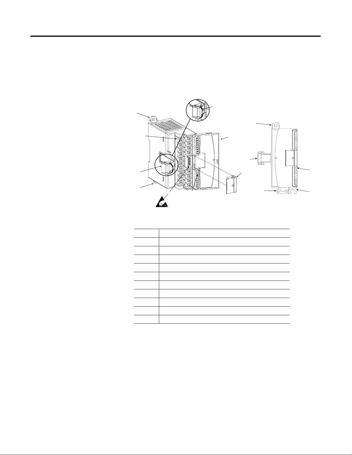
Hardware Features
The RTD/resistance module provides connections for four 3-wire
inputs for any combination of RTD and resistance input devices.
Channels are wired as differential inputs. The illustration below shows
the hardware features of the module.
1a
7
6
1b
4
2
9
1a
3
6
5
8
2
1b
Item Description
1a upper panel mounting tab
1b lower panel mounting tab
2 power diagnostic LED
3 module door with terminal identification label
4 bus connector with male pins
5 bus connector cover
6 flat ribbon cable with bus connector (female)
7 terminal block
8 DIN rail latch
9 pull loop
General Diagnostic Features
A single diagnostic LED helps you identify the source of problems that
may occur during power-up or during normal channel operation. The
LED indicates both status and power. See Chapter 4, Diagnostics and
Troubleshooting, for details on power-up and channel diagnostics.
Publication 1762-UM003A-EN-P - February 2003
Page 17

Overview 1-7
System Overview
The modules communicate to the local controller or communication
adapter through the 1762 bus interface. The modules also receive 5
and 24V dc power through the bus interface.
System Operation
At power-up, the module performs a check of its internal circuits,
memory, and basic functions. During this time, the module status LED
remains off. If no faults are found during power-up diagnostics, the
module status LED is turned on.
After power-up checks are complete, the module waits for valid
channel configuration data. If an invalid configuration is detected, the
module generates a configuration error. Once a channel is properly
configured and enabled, the module continuously converts the RTD
or resistance input to a value within the range selected for that
channel.
Each time the module reads an input channel, it tests the data for a
fault (over- or under-range, short-circuit, or open-circuit condition). If
it detects a fault, the module sets a unique bit in the channel status
word. See Input Data File on page 3-3.
Using the module image table, the controller reads the two’s
compliment binary converted input data from the module. This
typically occurs at the end of the program scan or when commanded
by the control program. If the controller and the module determine
that the data transfer has been made without error, the data is used in
the control program.
Publication 1762-UM003A-EN-P - February 2003
Page 18
1-8 Overview
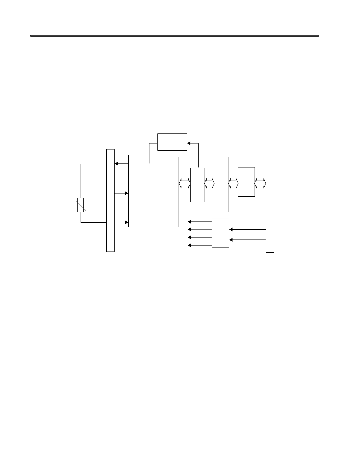
Input
EXC
Module Operation
As shown in the block diagram below, each input channel of the
module consists of an RTD/resistance connection that accepts
excitation current; a sense connection that detects lead wire
resistance; and a return connection. The signals are multiplexed to an
A/D converter that reads the RTD or resistance value and the lead
wire resistance.
Current
Source
A/D
Converter
MCU
ASIC
SENSE
RTN
Multiplexer
Te rm in al
+15V
+5V
A-GND
-15V
Opto-coupler
BUS
+24V dc
Isolation
Power Supply
S-GND
From the readings taken by the converter, the module returns an
accurate temperature or resistance to the controller user program
through the microprocessor. The module uses two bidirectional serial
ports for communication, each using an optocoupler for isolation. A
third optocoupler is used to reset the microprocessor if the module
detects a loss of communication.
Module Field Calibration
The input module performs autocalibration when a channel is initially
enabled. Autocalibration compensates for offset and gain drift of the
A/D converter caused by temperature change within the module. An
internal, high-precision, low drift voltage and system ground reference
is used for this purpose. In addition, you can program the module to
perform a calibration cycle once every 5 minutes. See Selecting
Enable/Disable Cyclic Autocalibration (Word 4, Bit 0) on page 3-20 for
information on configuring the module to perform periodic
calibration.
Publication 1762-UM003A-EN-P - February 2003
Page 19

Installation and Wiring
This chapter tells you how to:
• determine the power requirements for the modules
• avoid electrostatic damage
• install the module
• wire the module’s terminal block
• wire input devices
Chapter
2
Compliance to European Union Directives
This product is approved for installation within the European Union
and EEA regions. It has been designed and tested to meet the
following directives.
EMC Directive
The 1762-IR4 module is tested to meet Council Directive 89/336/EEC
Electromagnetic Compatibility (EMC) and the following standards, in
whole or in part, documented in a technical construction file:
• EN 50081-2
EMC – Generic Emission Standard, Part 2 - Industrial
Environment
• EN 50082-2
EMC – Generic Immunity Standard, Part 2 - Industrial
Environment
This product is intended for use in an industrial environment.
Low Voltage Directive
This product is tested to meet Council Directive 73/23/EEC Low
Voltage, by applying the safety requirements of EN 61131-2
Programmable Controllers, Part 2 – Equipment Requirements and
Tests.
1 Publication 1762-UM003A-EN-P - February 2003
Page 20

2-2 Installation and Wiring
For specific information required by EN61131-2, see the appropriate
sections in this publication, as well as the following Allen-Bradley
publications:
• Industrial Automation, Wiring and Grounding Guidelines for
Noise Immunity, publication 1770-4.1
• Automation Systems Catalog, publication B113
Power Requirements
General Considerations
The module receives +5V dc and 24V dc power from the system
power supply through the bus interface.
The maximum current drawn by the module is shown in the table
below.
5V dc 24V dc
40 mA 50 mA
TIP
When you configure your system, ensure that the
total current draw of all the modules does not
exceed the maximum current output of the system
power supply.
1762 I/O is suitable for use in an industrial environment when
installed in accordance with these instructions. Specifically, this
equipment is intended for use in clean, dry environments (Pollution
(1)
degree 2
) and to circuits not exceeding Over Voltage Category II
(IEC 60664-1).
(3)
(2)
Publication 1762-UM003A-EN-P - February 2003
(1) Pollution Degree 2 is an environment where, normally, only non-conductive pollution occurs except that
occasionally a temporary conductivity caused by condensation shall be expected.
(2) Over Voltage Category II is the load level section of the electrical distribution system. At this level transient
voltages are controlled and do not exceed the impulse voltage capability of the product’s insulation.
(3) Pollution Degree 2 and Over Voltage Category II are International Electrotechnical Commission (IEC)
designations.
Page 21
Installation and Wiring 2-3
Hazardous Location Considerations
This equipment is suitable for use in Class I, Division 2, Groups A, B,
C, D or non-hazardous locations only. The following WARNING
statement applies to use in hazardous locations.
WARNING
!
EXPLOSION HAZARD
• Substitution of components may impair
suitability for
Class I, Division 2.
• Do not replace components or disconnect
equipment unless power has been switched off
or the area is known to be non-hazardous.
• Do not connect or disconnect components
unless power has been switched off or the area
is known to be non-hazardous.
• This product must be installed in an enclosure.
• All wiring must comply with N.E.C. article
501-4(b).
Prevent Electrostatic Discharge
ATTENTION
Electrostatic discharge can damage integrated circuits
or semiconductors if you touch I/O module bus
connector pins or the terminal block on the input
module. Follow these guidelines when you handle
the module:
!
• Touch a grounded object to discharge static
potential.
• Wear an approved wrist-strap grounding device.
• Do not touch the bus connector or connector
pins.
• Do not touch circuit components inside the
module.
• If available, use a static-safe work station.
• When it is not in use, keep the module in its
static-shield box.
Publication 1762-UM003A-EN-P - February 2003
Page 22

2-4 Installation and Wiring
Remove Power
ATTENTION
Remove power before removing or inserting this
module. When you remove or insert a module with
power applied, an electrical arc may occur. An
electrical arc can cause personal injury or property
damage by:
!
• sending an erroneous signal to your system’s
field devices, causing unintended machine
motion
• causing an explosion in a hazardous
environment
Electrical arcing causes excessive wear to contacts
on both the module and its mating connector and
may lead to premature failure.
Selecting a Location
Reducing Noise
Most applications require installation in an industrial enclosure to
reduce the effects of electrical interference. RTD inputs are highly
susceptible to electrical noise. Electrical noise coupled to the RTD
inputs will reduce the performance (accuracy) of the module.
Publication 1762-UM003A-EN-P - February 2003
Group your modules to minimize adverse effects from radiated
electrical noise and heat. Consider the following conditions when
selecting a location for the module. Position the module:
• away from sources of electrical noise such as hard-contact
switches, relays, and AC motor drives
• away from modules which generate significant radiated heat.
Refer to the module’s heat dissipation specification.
In addition, route shielded, twisted-pair wiring away from any high
voltage I/O wiring.
Page 23
Mounting
Installation and Wiring 2-5
ATTENTION
!
Do not remove protective debris strip until after the
module and all other equipment near the module is
mounted and wiring is complete. Once wiring is
complete and the module is free of debris, carefully
remove the protective debris strip. Failure to remove
the strip before operating can cause overheating.
Minimum Spacing
Maintain spacing from enclosure walls, wireways, adjacent equipment,
etc. Allow 50.8 mm (2 in.) of space on all sides for adequate
ventilation, as shown below:
To p
Side Side
TIP
ATTENTION
MicroLogix
1200
1762 I/O may be mounted horizontally only.
During DIN rail or panel mounting of all devices, be
sure that all debris (metal chips, wire strands, etc.) is
kept from falling into the module. Debris that falls
into the module could cause damage at power up.
1762 I/O
1762 I/O
Bottom
!
1762 I/O
Publication 1762-UM003A-EN-P - February 2003
Page 24
2-6 Installation and Wiring
DIN Rail Mounting
The module can be mounted using the following DIN rails: 35 x 7.5
mm (EN 50 022 - 35 x 7.5) or 35 x 15 mm (EN 50 022 - 35 x 15).
Before mounting the module on a DIN rail, close the DIN rail latch.
Press the DIN rail mounting area of the module against the DIN rail.
The latch will momentarily open and lock into place.
Use DIN rail end anchors (Allen-Bradley part number 1492-EA35 or
1492-EAH35) for environments with vibration or shock concerns.
End Anchor
End Anchor
Publication 1762-UM003A-EN-P - February 2003
TIP
For environments with extreme vibration and
shock concerns, use the panel mounting method
described below, instead of DIN rail mounting.
Panel Mounting
Use the dimensional template shown below to mount the module.
The preferred mounting method is to use two M4 or #8 panhead
screws per module. M3.5 or #6 panhead screws may also be used, but
a washer may be needed to ensure a good ground contact. Mounting
screws are required on every module.
Page 25
For more than 2 modules: (number of modules - 1) x 40.4 mm (1.59 in.)
14.5
(0.57)
100
90
(3.94)
(3.54)
NOTE:
Hole spacing tolerance:
±0.4 mm (0.016 in.).
MicroLogix 1200
Installation and Wiring 2-7
40.4
(1.59)
Expansion I/O
MicroLogix 1200
MicroLogix 1200
MicroLogix 1200
Expansion I/O
Expansion I/O
40.4
(1.59)
System Assembly
The expansion I/O module is attached to the controller or another I/O
module by means of a ribbon cable after mounting as shown below.
IMPORTANT
WARNING
Use the pull loop on the connector to disconnect
modules. Do not pull on the ribbon cable.
EXPLOSION HAZARD
!
• In Class I, Division 2 applications, the bus
connector must be fully seated and the bus
connector cover must be snapped in place.
• In Class I, Division 2 applications, all modules
must be mounted in direct contact with each
other as shown on page 2-1. If DIN rail mounting
is used, an end stop must be installed ahead of
the controller and after the last 1762 I/O module.
Publication 1762-UM003A-EN-P - February 2003
Page 26

2-8 Installation and Wiring
Field Wiring Connections
System Wiring Guidelines
Consider the following when wiring your system:
General
• This product is intended to be mounted to a well-grounded
mounting surface such as a metal panel. Additional grounding
connections from the module’s mounting tabs or DIN rail (if
used) are not required unless the mounting surface cannot be
grounded.
• Channels are isolated from one another by ±10V dc maximum.
• Do not use the modules NC terminals as connection points.
• Route field wiring away from any other wiring and as far as
possible from sources of electrical noise, such as motors,
transformers, contactors, and ac devices. As a general rule, allow
at least 15.2 cm (6 in.) of separation for every 120V of power.
• Routing field wiring in a grounded conduit can reduce electrical
noise.
• If field wiring must cross ac or power cables, ensure that they
cross at right angles.
• To ensure optimum accuracy, limit overall cable impedance by
keeping your cable as short as possible. Locate the I/O system
as close to your sensors or actuators as your application will
permit.
• Tighten terminal screws with care. Excessive tightening can strip
a screw.
Publication 1762-UM003A-EN-P - February 2003
Shield Grounding
• Use Belden shielded, twisted-pair wire to ensure proper
operation and high immunity to electrical noise. Refer to the
following table and the RTD Wiring Considerations below.
Configuration
2-wire Belden™ 9501 or equivalent
3-wire
less than 30.48 m (100ft.)
3-wire
greater than 30.48 m (100 ft.) or high
humidity conditions
(1) For additional information, see page A-4.
• Under normal conditions, the drain wire and shield junction
should be connected to earth ground, via a panel or DIN rail
mounting screw at the 1762-IR4 module end.
Recommended Cable
Belden™ 9533 or equivalent
Belden™ 83503 or equivalent
(1)
Page 27

Installation and Wiring 2-9
• Keep shield connection to ground as short as possible.
• If noise persists for a device, try grounding the opposite end of
the cable. (You can only ground one end at a time.)
• Refer to Industrial Automation Wiring and Grounding
Guidelines, Allen-Bradley publication 1770-4.1, for additional
information.
RTD Wiring Considerations
Since the operating principle of the RTD module is based on the
measurement of resistance, take special care when selecting your
input cable. For 2-wire or 3-wire configurations, select a cable that has
a consistent impedance throughout its entire length. See Cable
Specifications on page A-4.
IMPORTANT
The RTD module requires three wires to
compensate for lead resistance error. We
recommend that you do not use 2-wire RTDs if long
cable runs are required, as it reduces the accuracy of
the system. However, if a two-wire configuration is
required, reduce the effect of the lead wire
resistance by using a lower gauge wire for the cable
(for example, use AWG #16 instead of AWG #24).
The module’s terminal block accepts two AWG #14
gauge wires.
When using a 3-wire configuration, the module compensates for
resistance error due to lead wire length. For example, in a 3-wire
configuration, the module reads the resistance due to the length of
one of the wires and assumes that the resistance of the other wire is
equal. If the resistances of the individual lead wires are much
different, an error may exist. The closer the resistance values are to
each other, the greater the amount of error that is eliminated.
IMPORTANT
To ensure temperature or resistance value accuracy,
the resistance difference of the cable lead wires
must be equal to or less than 0.01
Ω .
To insure that the lead values match as closely as possible:
• Keep lead resistance as small as possible and less than 25
• Use quality cable that has a small tolerance impedance rating.
• Use a heavy-gauge lead wire which has less resistance per foot.
Publication 1762-UM003A-EN-P - February 2003
Ω .
Page 28
2-10 Installation and Wiring
Wiring the Finger-Safe Terminal Block
ATTENTION
Be careful when stripping wires. Wire fragments that
fall into a module could cause damage when power
is applied. Once wiring is complete, ensure the
module is free of all metal fragments.
!
When wiring the terminal block, keep the finger-safe cover in place.
1. Route the wire under the terminal pressure plate. You can use
the stripped end of the wire or a spade lug. The terminals will
accept a 6.35 mm (0.25 in.) spade lug.
2. Tighten the terminal screw making sure the pressure plate
secures the wire. Recommended torque when tightening
terminal screws is 0.904 Nm (8 in-lbs).
3. After wiring is complete, remove the debris shield.
TIP
If you need to remove the finger-safe cover, insert a
screw driver into one of the square wiring holes and
gently pry the cover off. If you wire the terminal
block with the finger-safe cover removed, you will
not be able to put it back on the terminal block
because the wires will be in the way.
Publication 1762-UM003A-EN-P - February 2003
Page 29
Installation and Wiring 2-11
Wire Size and Terminal Screw Torque
Each terminal accepts up to two wires with the following restrictions:
Wire Type Wire Size Terminal Screw Torque
Solid Cu-90°C (194°F) #14 to #22 AWG 0.904 Nm (8 in-lbs)
Stranded Cu-90°C (194°F) #16 to #22 AWG 0.904 Nm (8 in-lbs)
Wiring Input Devices to the Module
ATTENTION
To prevent shock hazard, care should be taken when
wiring the module to analog signal sources. Before
wiring any module, disconnect power from the
system power supply and from any other source to
the module.
!
After the module is properly installed, follow the wiring procedure
below and the RTD and potentiometer wiring diagrams on pages 2-12
through 2-15. To ensure proper operation and high immunity to
electrical noise, always use Belden™ shielded, twisted-pair or
equivalent wire.
Cut foil shield
and drain wire
signal wire
signal wire
signal wire
signal wire
drain wire
cable
foil shield
signal wire
signal wire
signal wire
drain wire
foil shield
cable
Publication 1762-UM003A-EN-P - February 2003
Cut foil shield
and drain wire
signal wires (3)
Page 30
2-12 Installation and Wiring
To wire your module follow these steps:
1. At each end of the cable, strip some casing to expose the
individual wires.
2. Trim the signal wires to 2-inch (5 cm) lengths. Strip about 3/16
inch (5 mm) of insulation away to expose the end of the wire.
ATTENTION
Be careful when stripping wires. Wire fragments that
fall into a module could cause damage at power up.
!
3. At the module end of the cable, twist the drain wire and foil
shield together, bend them away from the cable, and apply
shrink wrap. Then earth ground via a panel or DIN rail
mounting screw at the end of the module. Keep the length of
the drain wire as short at possible.
4. At the other end of the cable, cut the drain wire and foil shield
back to the cable and apply shrink wrap.
5. Connect the signal wires to the terminal block as described for
each type of input. See Wiring RTDs on page 2-12 or Wiring
Resistance Devices (Potentiometers) on page 2-14.
6. Connect the other end of the cable to the analog input device.
Publication 1762-UM003A-EN-P - February 2003
7. Repeat steps 1 through 6 for each channel on the module.
Wiring RTDs
Three types of RTDs can be connected to the 1762-IR4 module:
• 2-wire RTD, which is composed of an RTD EXC (excitation) lead
wire and a RTN (return) lead wire
• 3-wire RTD, which is composed of a Sense and 2 RTD lead
wires (RTD EXC and RTN)
• 4-wire RTD, which is composed of a Sense and 2 RTD lead
wires (RTD EXC and RTN). The second sense wire from the
4-wire RTD is left open.
Page 31

2-Wire RTD Configuration
Installation and Wiring 2-13
Cable Shield (to Ground)
SENSE 2
IMPORTANT
EXC 2
RTN 2
NC
RTD EXC
Return
Belden 9501 Shielded Cable
RTD EXC
Return
Using 2-wire configurations does not permit the
module to compensate for resistance error due to
lead wire length. The resulting analog data includes
the effect of this uncompensated lead wire resistance.
The module continues to place the uncompensated
analog data in the input data file, but the open-circuit
status bit (OCx) is set in word 4 of the input data file
for any enabled channel using a 2-wire configuration.
These status bits may be used in the control program
to indicate that the analog data includes error due to
uncompensated lead wires. See page 3-4 for a
detailed discussion of the open-circuit status bits.
3-Wire RTD Configuration
EXC 2
SENSE 2
RTN 2
NC
Cable Shield (to Ground)
RTD EXC
Sense
Return
RTD EXC
Sense
Return
Belden 83503 or 9533 Shielded Cable
Publication 1762-UM003A-EN-P - February 2003
Page 32

2-14 Installation and Wiring
4-Wire RTD Configuration
Cable Shield (to Ground)
RTD EXC
RTD EXC
EXC 2
Sense
Sense
SENSE 2
Return
Return
RTN 2
NC
Belden 83503 or 9533 Shielded Cable
Leave one sensor wire open.
Wiring Resistance Devices (Potentiometers)
Potentiometer wiring requires the same type of cable as that for the
RTDs described on page 2-9. Potentiometers can be connected to the
module as a 2-wire or 3-wire connection as shown on page 2-14.
2-Wire Potentiometer Interconnection
Cable Shield (to Ground)
RTD EXC
EXC 2
Potentiometer
SENSE 2
RTN 2
NC
EXC 2
SENSE 2
RTN 2
NC
TIP
Return
Belden 9501 Shielded Cable
Cable Shield (to Ground)
RTD EXC
Return
Belden 9501 Shielded Cable
Potentiometer
The potentiometer wiper arm can be connected to
either the EXC or return terminal depending on
whether you want increasing or decreasing
resistance.
Publication 1762-UM003A-EN-P - February 2003
Page 33

Installation and Wiring 2-15
EXC 2
SENSE 2
RTN 2
IMPORTANT
Using 2-wire configurations does not permit the
module to compensate for resistance error due to
lead wire length. The resulting analog data includes
the effect of this uncompensated lead wire resistance.
The module continues to place the uncompensated
analog data in the input data file, but the open-circuit
status bit (OCx) is set in word 4 of the input data file
for any enabled channel using a 2-wire configuration.
These status bits may be used in the control program
to indicate that the analog data includes error due to
uncompensated lead wires. See page 3-4 for a
detailed discussion of the open-circuit status bits.
3-Wire Potentiometer Interconnection
Run RTD and sense wires from the module to
Cable Shield (to Ground)
RTD EXC
Sense
Return
potentiometer terminal and tie terminal to one point.
Potentiometer
NC
EXC 2
SENSE 2
RTN 2
NC
Cable Shield (to Ground)
RTD EXC
Sense
Return
TIP
Belden 83503 or 9533 Shielded Cable
Run RTD and sense wires from the module to
potentiometer terminal and tie terminal to one point.
Potentiometer
Belden 83503 or 9533 Shielded Cable
The potentiometer wiper arm can be connected to
either the EXC or return terminal depending on
whether you want increasing or decreasing
resistance.
Publication 1762-UM003A-EN-P - February 2003
Page 34

2-16 Installation and Wiring
Publication 1762-UM003A-EN-P - February 2003
Page 35

Chapter
3
Module Data, Status, and Channel
Configuration
After installing the 1762-IR4 RTD/resistance input module, you must
configure it for operation, usually using the programming software
compatible with the controller (for example, RSLogix 500™). Once
configuration is complete and reflected in ladder logic, you will need
to get the module up and running and then verify its operation. This
chapter includes information on the following:
• module memory map
• accessing input image file data
• configuring channels
• configuring periodic calibration
• preparing ladder logic to reflect the configuration
• running the module
• verifying the configuration
Module Memory Map
slot e
Input Image
File
slot e
Configuration
File
The module uses six input words for data and status bits (input
image), and five configuration words.
Word 0
Word 1
Word 2
Word 3
Word 4
Word 5
Word 0
Word 1
Word 2
Word 3
Word 4
Input Image
6 words
Configuration
File
5 words
Channel 0 Data Word
Channel 1 Data Word
Channel 2 Data Word
Channel 3 Data Word
General/Open-Circuit Status Bits
Over-/Under-range Bits
Channel 0 Configuration Word
Channel 1 Configuration Word
Channel 2 Configuration Word
Channel 3 Configuration Word
Enable Calibration Word
Bit 15 Bit 0
1 Publication 1762-UM003A-EN-P - February 2003
Page 36

3-2 Module Data, Status, and Channel Configuration
Input Image
The input image file represents data words and status words. Input
words 0 through 3 hold the input data that represents the value of the
analog inputs for channels 0 through 3. These data words are valid
only when the channel is enabled and there are no errors. Input
words 4 and 5 hold the status bits. To receive valid status information,
the channel must be enabled.
Configuration File
The configuration file contains information that you use to define the
way a specific channel functions. The configuration file is explained in
more detail in Configuration Data File on page 3-6.
Accessing Input Image File Data
TIP
Six words of the processor input image table are reserved for the
module’s image data. You can access the information in the input
image file using the programming software configuration screen. For
more information on configuration using MicroLogix 1200 and
RSLogix 500, see Appendix B.
Not all controllers support program access to the
configuration file. Refer to your controller’s user
manual.
Publication 1762-UM003A-EN-P - February 2003
Page 37

Module Data, Status, and Channel Configuration 3-3
Input Data File
The input data table allows you to access RTD input module read data
for use in the control program, via word and bit access. The data table
structure is shown in table below.
Table 3.1 Input Data Table
Word/Bit1514131211109876543210
0 RTD/Resistance Input Data Channel 0
1 RTD/Resistance Input Data Channel 1
2 RTD/Resistance Input Data Channel 2
3 RTD/Resistance Input Data Channel 3
4 Reserved OC3 OC2 OC1 OC0 Reserved S3 S2 S1 S0
5 U0 O0U1O1U2O2U3O3 Reserved
Input Data Values
Data words 0 through 3 correspond to channels 0 through 3 and
contain the converted analog input data from the input device.
TIP
Status bits for a particular channel reflect the
configuration settings for that channel. To receive
valid status, the channel must be enabled and the
module must have stored a valid configuration word
for that channel.
General Status Flag Bits (S0 to S3)
Bits S0 through S3 of Word 3 contain the general status information for
channels 0 through 3, respectively. This bit is set (1) when an error
(over- or under-range, short-circuit, open-circuit, or input data not
valid) exists for that channel. The error conditions of the General
Status bits are logically ORed. Therefore, the user control program
determines which condition is setting the general status bit by viewing
the following bits: open-circuit, over-range, or under-range. The data
not valid condition is described on the following page.
Publication 1762-UM003A-EN-P - February 2003
Page 38

3-4 Module Data, Status, and Channel Configuration
Input Data Not Valid Condition
The general status bits S0 to S3 also indicate whether or not the input
data for a particular channel, 0 through 3, is being properly converted
(valid) by the module. This “invalid data” condition can occur (bit set)
when the download of a new configuration to a channel is accepted
by the module (proper configuration) but before the A/D converter
can provide valid (properly configured) data to the MicroLogix 1200
controller. The following information highlights the bit operation of
the Data Not Valid condition.
1. The default and module power-up bit condition is reset (0).
2. The bit condition is set (1) when a new configuration is received
and determined valid by the module. The set (1) bit condition
remains until the module begins converting analog data for the
previously accepted configuration. When conversion is
complete, the bit condition is reset (0) by the module. The
amount of time it takes for the module to begin the conversion
process depends on the number of channels being configured
and the amount of configuration data downloaded by the
controller.
TIP
3. If A/D hardware errors prevent the conversion process from
taking place, the bit condition is set (1).
If the new configuration is invalid, the bit
function remains reset (0) and the module posts
a configuration error. See Configuration Errors
on page 4-6.
Open-Circuit Flag Bits (OC0 to OC3)
Bits OC0 through OC3 of word 4 contain open-circuit error
information for channels 0 through 3, respectively. For an RTD input,
the bits indicate either an open-circuit or short-circuit condition when
set (1). For a resistance input, the bits indicate an open-circuit when
set (1).
TIP
Short-circuit detection for direct resistance inputs is
not indicated because 0 is a valid number.
Publication 1762-UM003A-EN-P - February 2003
Page 39

Module Data, Status, and Channel Configuration 3-5
Over-Range Flag Bits (O0 to O3)
Over-range bits for channels 0 through 3 are contained in word 5,
even-numbered bits. They apply to all input types. When set (1), the
over-range flag bit indicates an RTD temperature that is greater than
the maximum allowed temperature or a resistance input that is greater
than the maximum allowed resistance for the module. The module
automatically resets (0) the bit when the data value is again within the
normal operating range.
Under-Range Flag Bits (U0 to U3)
Under-range bits for channels 0 through 3 are contained in word 5,
odd-numbered bits. They apply only to RTD input types. When set
(1), the under-range flag bit indicates an RTD temperature that is less
than the minimum allowed temperature. The module automatically
resets (0) the bit when the data value is again within the normal
operating range.
Configuring Channels
TIP
After module installation, you must configure operation details, such
as RTD type, temperature units, etc., for each channel. Channel
configuration data for the module is stored in the controller
configuration file, which is both readable and writable.
There is no under-range error for a direct resistance
input, because 0 is a valid number.
Publication 1762-UM003A-EN-P - February 2003
Page 40

3-6 Module Data, Status, and Channel Configuration
Configuration Data File
The configuration data file is shown below. Bit definitions are
provided in Channel Configuration on page 3-7. Detailed definitions
of each of the configuration parameters follows the table.
TIP
Normal channel configuration is done using
programming software. In that case, it is not
necessary to know the meaning of the bit
location. However, some systems allow
configuration to be changed by the control
program. Refer to your controller’s
documentation for details.
The default configuration of the table is all zeros, which yields the
following.
Table 3.2 Default Configuration
Parameter Default Setting
Channel Enable/Disable Disable
Data Format Raw/Proportional
Input/Sensor Type 100Ω Platinum 385
Temperature Units/Mode °C (not applicable with Raw/Proportional)
Open/Broken Circuit Response Upscale
Cyclic Lead Compensation Enable
Excitation Current 1.0 mA
Publication 1762-UM003A-EN-P - February 2003
Input FIlter Frequency 60 Hz
Page 41

Table 3.3 Configuration Data File
Module Data, Status, and Channel Configuration 3-7
The following table shows the basic arrangement of the configuration
data file.
Word/
Bit
0 Enable/
1 Enable/
2 Enable/
3 Enable/
4 Not Used Enable/Disable
15 14 13 12 11 10 9 8 7 6 5 4 3 2 1 0
Disable
Channel 0
Disable
Channel 1
Disable
Channel 2
Disable
Channel 3
Data
Format
Channel 0
Data
Format
Channel 1
Data
Format
Channel 2
Data
Format
Channel 3
Input/Sensor
Type Channel 0
Input/Sensor
Type Channel 1
Input/Sensor
Type Channel 2
Input/Sensor
Type Channel 3
Temperature
Units/Mode
Channel 0
Temperature
Units/Mode
Channel 1
Temperature
Units/Mode
Channel 2
Temperature
Units/Mode
Channel 3
Open/
Broken
Circuit
Response
Channel 0
Open/
Broken
Circuit
Response
Channel 1
Open/
Broken
Circuit
Response
Channel 2
Open/
Broken
Circuit
Response
Channel 3
Cyclic Lead
Compensation
Channel 0
Cyclic Lead
Compensation
Channel 1
Cyclic Lead
Compensation
Channel 2
Cyclic Lead
Compensation
Channel 3
Excitation
Current
Channel 0
Excitation
Current
Channel 1
Excitation
Current
Channel 2
Excitation
Current
Channel 3
Filter Frequency
Filter Frequency
Filter Frequency
Filter Frequency
Channel 0
Channel 1
Channel 2
Channel 3
Cyclic
Calibration
(1)
(1) When enabled, an autocalibration cycle is performed on all enabled channels every 5 minutes.
Channel Configuration
Words 0 to 3 of the configuration file allow you to change the
parameters of each channel independently. For example, word 0
corresponds to channel 0, word 1 to channel 1, etc. The functional
arrangement of the bits for one word is shown in the table on page
3-8.
Publication 1762-UM003A-EN-P - February 2003
Page 42

3-8 Module Data, Status, and Channel Configuration
Table 3.4 Channel Configuration Bit Definitions
To Select Make these bit settings
1514131211109876543210
10 Hz
60 Hz
Filter Frequency
50 Hz
250Hz
500 Hz
1 kHz
Excitation
Current
Cyclic Lead
Compensation
1.0 mA
0.5 mA
Enable
Disable
Upscale
Open/Broken
Circuit Response
Downscale
Last State
Zero
Temperature
Units/Mode
Input/Sensor
Typ e
Data Format
Enable/Disable
Channel
°C 0 0
(1)
°F
100Ω Platinum 385
200Ω Platinum 385
500Ω Platinum 385
1000Ω Platinum 385
100Ω Platinum 3916
200Ω Platinum 3916
500Ω Platinum 3916
1000Ω Platinum 3916
10 Copper 426
(3)
120 Nickel 618
120 Nickel 672
604 Nickel-Iron 518
150 Ω
500 Ω
1000 Ω
(2)
3000Ω
Raw/Proportional
Engineering Units
Engr. Units X 10
Scaled-for-PID
Percent Range
(2)
(2)
000 0
001 4096
100 16384
010 8192
011 12288
0000 0
0001 256
0010 512
0011 768
0100 1024
0101 1280
0110 1536
0111 1792
1000 2048
1001 2304
1010 2560
1011 2846
1100 3072
1101 3328
1110 3584
1111 3840
Enable 1
Disable 0
Decimals
110 6
000 0
001 1
011 3
100 4
101 5
0 0
1 8
0 0
1 16
00 0
01 32
10 64
11 96
1 128
-32768
0
(1) Ignored for a resistance device input.
(2) Valid only with the 0.5 mA excitation current.
(3) Valid only with the 1.0 mA excitation current.
Publication 1762-UM003A-EN-P - February 2003
Page 43

Module Data, Status, and Channel Configuration 3-9
Enabling or Disabling a Channel (Bit 15)
Bit 15 enables or disables each of the six channels individually. The
module only scans those channels that are enabled. Enabling a
channel forces it to be recalibrated before it measures input data.
Turning a channel off results in the channel data being set to zero.
TIP
When a channel is not enabled, the A/D converter
provides no input to the controller. This speeds up
the system response of the active channels.
The configuration default is to disable each input
channel to maximize module performance.
Selecting Data Format (Bits 12 to 14)
Bits 12 through 14 of the channel configuration word are used to
indicate the input data format. You may choose any of the following
formats:
• raw/proportional
• engineering units x 1
• engineering units x 10
• scaled for PID
• percent of full scale
TIP
The engineering units data formats represent real
temperature or resistance engineering units provided
by the module. The raw/proportional counts,
scaled-for-PID, and percent of full scale data formats
The raw/proportional counts, scaled-for-PID and
percent of full-scale data formats may yield the
highest effective resolutions, but may also require
that you convert channel data to real engineering
units in your control program.
Publication 1762-UM003A-EN-P - February 2003
Page 44

3-10 Module Data, Status, and Channel Configuration
Table 3.5 Data Formats for RTD Temperature Ranges for 0.5 and 1.0 mA Excitation Current
Data Format
RTD Input Type
100Ω Platinum 385 -2000 to +8500 -3280 to +15620 -200 to +850 -328 to +1562
200Ω Platinum 385 -2000 to +8500 -3280 to +15620 -200 to +850 -328 to +1562
500Ω Platinum 385 -2000 to +8500 -3280 to +15620 -200 to +850 -328 to +1562
1000Ω Platinum 385 -2000 to +8500 -3280 to +15620 -200 to +850 -328 to +1562
100Ω Platinum 3916 -2000 to +6300 -3280 to +11660 -200 to +630 -328 to +1166
200Ω Platinum 3916 -2000 to +6300 -3280 to +11660 -200 to +630 -328 to +1166
500Ω Platinum 3916 -2000 to +6300 -3280 to +11660 -200 to +630 -328 to +1166
1000Ω Platinum 3916 -2000 to +6300 -3280 to +11660 -200 to +630 -328 to +1166
10Ω Copper 426 -1000 to +2600 -1480 to +5000 +100 to +260 -148 to +500
120Ω Nickel 618 -1000 to +2600 -1480 to +5000 -100 to +260 -148 to +500
120Ω Nickel 672 -800 to +2600 -1120 to +5000 -80 to +260 -112 to +500
604Ω Nickel Iron 518 -1000 to +2000 -3280 to +3920 -100 to +200 -328 to +392
Engineering Units x1 Engineering Units x10
0.1°C 0.1°F 1.0°C 1.0°F
Scaled-
for-PID
0
to
16383
Proportional
Counts
-32768
to
+32767
Percent of
Full Scale
0
to
+10000
Raw/Proportional Data Format
The raw/proportional data format provides the greatest resolution of
all the data formats. For this format, the value presented to the
controller is proportional to the selected input. It is also scaled to the
maximum data range allowed by the bit resolution of the A/D
converter and selected filter frequency.
If you select the raw/proportional data format for a channel, the data
word will be a linearized number between -32768 and +32767. The
value -32768 corresponds to the lowest temperature value for an RTD
or the lowest resistance value for a resistance device.
Publication 1762-UM003A-EN-P - February 2003
Page 45

Module Data, Status, and Channel Configuration 3-11
Figure 3.1 Linear Relationship Between Temperature and Proportional Counts
Counts
+ 32,767
EXAMPLE
±200 ˚C
850 ˚C
-32,768
°C
The value +32767 corresponds to the highest value for the device. For
example, if a 100Ω platinum 385 RTD is selected, the lowest
temperature of -200°C corresponds to -32768 counts. The highest
temperature of 850°C corresponds to +32767 counts. See Determining
Effective Resolution and Range on page 3-20.
Scaling Examples
Scaled-for-PID to Engineering Units x1
• input type = 200Ω Platinum RTD
•α = 0.00385°C
• range = -200 to +850°C S
• channel data = 3421(scaled-for-PID)
= -200°C S
LOW
HIGH
= +850°C
Engineering Units Equivalent = S
LOW
+ (S
HIGH
- S
) x (channel data/16383)]
LOW
Engineering Units Equivalent = -200°C + [(+850°C -(-200°C)) x (3421/16383)] =
19.25°C
Publication 1762-UM003A-EN-P - February 2003
Page 46

3-12 Module Data, Status, and Channel Configuration
EXAMPLE
EXAMPLE
Engineering Units x1 to Scaled-for-PID
• input type = 200Ω Platinum RTD
•α = 0.00385°C
• range = -200 to +850°C S
= -200°C S
LOW
HIGH
= +850°C
• desired channel temperature = 344°C (engineering units)
Scaled-for-PID Equivalent = 16383 x [(desired ch. temp. - S
LOW
)/(S
HIGH
- S
LOW
)]
Scaled-for-PID Equivalent = 16383 x [(344°C - (-200°C))/(850°C - (-200°C))] = 8488
Proportional Counts to Engineering Units x1
• input type = 1000Ω potentiometer
• range = 0 to 1000Ω S
• channel data = 21567 (proportional counts)
Engineering Units Equivalent =
S
LOW
+ {(S
HIGH
- S
) x [(ch. data + 32768)/65536]}
LOW
Engineering Units Equivalent =
0 + {(1000 - 0) x [(21567 + 32768)/65536]} = 829Ω
= 0Ω S
LOW
HIGH
= 1000Ω
EXAMPLE
Engineering Units x1 to Proportional Counts
• input type = 3000Ω potentiometer
• range = 0 to 3000Ω S
• desired channel resistance = 1809Ω (engineering units x 1)
Prop. Counts Equivalent =
{65536 x [(ch. resistance - S
Proportional Counts Equivalent =
{65536 x [(1809Ω - 0) / (3000 − 0) ] } − 32768 = 6750
= 0Ω S
LOW
LOW
)/(S
HIGH
HIGH
- S
= 3000Ω
)]} - 32768
LOW
Publication 1762-UM003A-EN-P - February 2003
Page 47

Module Data, Status, and Channel Configuration 3-13
Engineering Units x 1 Data Format
If you select engineering units x 1 as the data format for an RTD input,
the module scales input data to the actual temperature values for the
selected RTD type per RTD standard. It expresses temperatures in
0.1°C units. For resistance inputs, the module expresses resistance in
0.1Ω units, for all ranges except the 150Ω range. For the latter,
resistance is expressed in 0.01Ω units.
TIP
Use the engineering units x 10 setting to produce
temperature readings in whole degrees Celsius or
Fahrenheit. See Engineering Units x 10 Data Format
below.
The resolution of the engineering units x 1 format is dependent on the
range selected and the filter selected. See Determining Effective
Resolution and Range on page 3-20.
Engineering Units x 10 Data Format
For the engineering units x 10 data format for an RTD input, the
module scales input data to the actual temperature values for the
selected RTD type per RTD standard. With this format, the module
expresses temperatures in 1°C units. For resistance inputs, the module
expresses resistance in 1Ω units, for all ranges except the 150Ω range.
For the latter, resistance is expressed in 0.1Ω units.
The resolution of the engineering units x 10 format is dependent on
the range selected and the filter selected. See Determining Effective
Resolution and Range on page 3-20.
Scaled-for-PID Data Format
If you select the scaled-for-PID data format, the module presents to
the controller a signed integer representing the input signal range
proportional to the selected input type. The integer value is the same
for RTD and resistance input types.
To obtain the value, the module scales the input signal range to a
linearized 0 to 16383 range, which is standard to the PID algorithm for
the MicroLogix, SLC, and PLC controllers. The 0 value corresponds to
the lowest temperature or resistance value, while 16383 corresponds
to the highest value. For example, if a 100Ω platinum 385 RTD is
selected, the lowest temperature for the RTD, -200° C, corresponds to
0. The highest temperature, 850°C, corresponds to 16383.
Publication 1762-UM003A-EN-P - February 2003
Page 48

3-14 Module Data, Status, and Channel Configuration
Linear Relationship Between Temperature and PID Counts
Counts
+16383
+850 ˚C -200 ˚C
°C
The amount over and under user range (full-scale range -410 to
+16793) is also included in the signed integer provided to the
controller. Allen-Bradley controllers, such as the MicroLogix 1500, use
this range in their PID equations. See Determining Effective
Resolution and Range on page 3-20.
Percent of Full Scale Data Format
With the percent of full scale data format, the module presents input
data to the user as a percent of the user-specified range. For example,
for a 100Ω platinum 385 RTD, the range -200×C to 850×C is
represented as 0 percent to 100 percent. See Determining Effective
Resolution and Range on page 3-20.
Publication 1762-UM003A-EN-P - February 2003
Selecting Input/Sensor Type (Bits 8 to 11)
You can set bits 8 through 11 in the channel configuration word to
indicate the type of input sensor, for example, 100Ω platinum 385
RTD. Each channel can be configured for any input type. The valid
input types and bit settings are listed in the channel configuration
table on page 3-7.
Page 49

Module Data, Status, and Channel Configuration 3-15
Selecting Temperature Units/Mode (Bit 7)
The module supports two different linearized, scaled temperature
ranges for RTDs, degrees Celsius (°C) and degrees Fahrenheit (°F).
You can select the type that is appropriate for your application by
setting bit 7 in the channel configuration word. Bit 7 is ignored for
resistance input types or when raw/proportional, scaled-for-PID, or
percent data formats are used.
Selecting Open-Circuit Response (Bits 5 and 6)
Broken inputs for the module include open-circuit and short-circuit
conditions. An open-circuit occurs when the module’s maximum input
voltage is reached. This can happen if the wire is cut or disconnected
from the terminal block. The module can encounter an open-circuit
for any RTD or resistance input.
A short-circuit occurs when the calculated lead wire compensated
resistance is less than 3Ω . The module can only report a short-circuit
for an RTD.
Use bits 5 and 6 of channel configuration word to define the state of
the channel data word when a broken input condition is detected for
the corresponding channel. When it detects an open circuit or a short
circuit, the module overrides the actual input data with the value that
you specify.
Table 3.6 Open/Broken Circuit Response Definitions
Open/Broken
Circuit Value
Upscale Sets input to full upper scale value of channel data word. The full-scale
Downscale Sets input to full lower scale value of channel data word. The low scale
Last State Sets input to last input value.
Zero Sets input to 0 to force the channel data word to 0.
Response Definition
value is determined by the selected input type, data format, and scaling.
value is determined by the selected input type, data format, and scaling.
Publication 1762-UM003A-EN-P - February 2003
Page 50

3-16 Module Data, Status, and Channel Configuration
Selecting Cyclic Lead Compensation (Bit 4)
For each channel, the module measures lead resistance in one of two
ways. Set bit 4 to 0 to enable measurement and compensation of lead
resistance every five minutes. One channel is measured per module
update to limit the impact to channel throughput. You can also
implement a lead wire calibration cycle any time, at your command,
by enabling and then disabling this bit in your control program.
Regardless of the state of bit 4, lead wire compensation occurs
automatically on a system mode change from Program-to-Run or if
any online configuration change is made to a channel.
Selecting Excitation Current (Bit 3)
The module is capable of exciting each individual RTD/resistance
device with either 0.5 mA or 1.0 mA of current. Setting bit 3 to 0
provides 1.0 mA, while a setting of 1 provides 0.5 mA.
The 0.5 mA excitation current is recommended for use with 1000Ω
RTDs and 3000Ω direct resistance inputs. An excitation current of 1.0
mA is recommended for all other RTDs except the 1000Ω devices, and
all other direct resistance devices except the 3000Ω devices. Refer to
the input device literature for the manufacturer’s recommendations.
TIP
A lower excitation current reduces error due to RTD
self-heating, but provides a lower signal-to-noise
ratio. See the manufacturer’s recommendations for
your particular RTD.
Setting Filter Frequency (Bits 0 to 2)
The module supports filter selections corresponding to filter
frequencies of 10 Hz, 50 Hz, 60 Hz, 250 Hz, 500 Hz, and 1 kHz. Your
filter frequency selection is determined by the desired range for the
input type, and the required effective resolution, which indicates the
number of bits in the channel configuration word that do not vary due
to noise. Also consider the required module update time when
choosing a filter frequency. For example, the 10 Hz filter provides the
greatest attenuation of 50 and 60 Hz noise and the greatest resolution,
but also provides the slowest response speed.
Publication 1762-UM003A-EN-P - February 2003
Page 51

Module Data, Status, and Channel Configuration 3-17
The choice that you make for filter frequency will affect:
• noise rejection characteristics for module input
• channel step response
• channel cutoff frequency
• module autocalibration
• effective resolution
• module update time
Effects of Filter Frequency on Noise Rejection
The filter frequency that you choose for a channel determines the
amount of noise rejection for the inputs. A smaller filter frequency
(e.g. 10Hz) provides the best noise rejection and increases effective
resolution, but also increases channel update time. A larger filter
frequency (e.g. 1 kHz) provides lower noise rejection, but also
decreases the channel update time and effective resolution.
When selecting a filter frequency, be sure to consider channel cutoff
frequency and channel step response to obtain acceptable noise
rejection. Choose a filter frequency so that your fastest-changing
signal is below that of the filter’s cutoff frequency.
Common mode noise rejection for the module is better than 110 dB at
50 Hz (50 Hz filter) and 60 Hz (60 Hz filter). The module performs
well in the presence of common mode noise as long as the signals
applied to the input terminals do not exceed the common mode
voltage rating (±10V) of the module. Improper earth ground can be a
source of common mode noise.
TIP
Transducer power supply noise, transducer circuit
noise, and process variable irregularities can also be
sources of common mode noise.
Channel Step Response
Another module characteristic determined by filter frequency is
channel step response, as shown in the following table. The step
response is the time required for the analog input signal to reach 100
percent of its expected final value, given a full-scale step change in
the input signal. Thus, if an input signal changes faster than the
channel step response, a portion of that signal will be attenuated by
Publication 1762-UM003A-EN-P - February 2003
Page 52

3-18 Module Data, Status, and Channel Configuration
the channel filter. The channel step response is calculated by a settling
time of 3 x (1 / filter frequency).
Table 3.7 Filter Frequency vs. Channel Step Response
Filter Frequency Step Response Filter Frequency Step Response
Channel Cutoff Frequency
The channel cutoff frequency (-3 dB) is the point on the input channel
frequency response curve where frequency components of the input
signal are passed with 3 dB of attenuation. The following table shows
cutoff frequencies for the supported filters.
Table 3.8 Filter Frequency vs. Channel Cutoff Frequency
Filter Frequency Channel Cutoff Frequency
10 Hz 2.62 Hz
10 Hz 300 ms 250 Hz 12 ms
50 Hz 60 ms 500 Hz 6 ms
60 Hz 50 ms 1 kHz 3 ms
50 Hz 13.1 Hz
60 Hz 15.7 Hz
250 Hz 65.5 Hz
500 Hz 131 Hz
1 kHz 262 Hz
All frequency components at or below the cutoff frequency are passed
by the digital filter with less than 3 dB of attenuation. All frequency
components above the cutoff frequency are increasingly attenuated,
as shown in the graphs below for several of the input filter
frequencies.
TIP
Channel cutoff frequency should not be confused
with channel update time. The cutoff frequency
simply determines how the digital filter attenuates
frequency components of the input signal. See
Determining Module Update Time on page 3-27.
Publication 1762-UM003A-EN-P - February 2003
Page 53

Frequency Response Graphs
Module Data, Status, and Channel Configuration 3-19
0
–20
–40
–60
–80
-100
-120
Gain (dB)
-140
-160
-180
- 200
0
2.62 Hz
0
–20
–40
–60
–80
-100
Gain (dB)
-120
-140
-160
-180
- 200
15 .72 Hz
10 Hz Input Filter Frequency
–20
–40
–60
–80
-100
-120
Gain (dB)
-140
-160
-180
- 200
0
0
13. 1 Hz
–3 dB
50
–3 dB
10
20
30
40
50
60
Frequency (Hz)
60 Hz Input Filter Frequency
–20
–40
–60
–80
-100
Gain (dB)
-120
-140
-160
-180
- 200
0
–3 dB
0
65 .5 Hz
–3 dB
0
60
120
180
240
300
360
Frequency (Hz)
50 Hz Input Filter Frequency
100
150
200
Frequency (Hz)
250 Hz Input Filter Frequency
900
Frequency (Hz)
250
300
1300
1150750500250
0
–20
–40
–60
–80
-100
Gain (dB)
-120
-140
-160
-180
- 200
131 Hz
–3 dB
500 Hz Input Filter Frequency
2000
Frequency (Hz)
1 kHz Input Filter Frequency
0
–20
–40
–60
–80
-100
Gain (dB)
-120
-140
-160
-180
30000 250015001000500
- 200
0
262 Hz
–3 dB
4K
Frequency (Hz)
5K3K2K1K
6K
Publication 1762-UM003A-EN-P - February 2003
Page 54

3-20 Module Data, Status, and Channel Configuration
Selecting Enable/Disable Cyclic Autocalibration (Word 4, Bit 0)
Configuration word 4, bit 0 allows you to configure the module to
perform an autocalibration cycle of all enabled channels once every 5
minutes. Cyclic calibration functions to reduce offset and gain drift
errors due to temperature changes within the module. Setting this bit
to 1 disables cyclic calibration, the default (0) enables the
autocalibration function. See Effects of Autocalibration on Accuracy
on page 3-33.
Determining Effective Resolution and Range
TIP
This section provides tables showing effective resolution and range
for all possible input data types at each filter frequency. Look up your
required resolution, range, and input type in the tables. Choose the
frequency that most closely matches your requirements.
For systems that allow modifying the state of this bit,
you can program the autocalibration cycle to occur
whenever you desire via the ladder program, by
cycling the bit from 0 to 1.
Publication 1762-UM003A-EN-P - February 2003
Page 55

Table 3.9 Effective Resolution and Range for 10 Hz Filter Frequency
Module Data, Status, and Channel Configuration 3-21
Raw/Proportional Data
Over Full Input Range
Input
Ty pe
Decimal
100Ω
Pt 385
200Ω
Pt 385
500Ω
Pt 385
1000Ω
Pt 385
100Ω
Pt
3916
200Ω
Pt
3916
500Ω
Pt
3916
1000Ω
Pt
3916
10Ω
Cu 426
120Ω
Ni 618
120Ω
Ni 672
604Ω
NiFe
518
150Ω 0.039Ω / 17 counts 0 to
500Ω 0.046Ω / 6 counts 0 to
1000Ω 0.092Ω / 6 counts 0 to
3000Ω 0.320Ω / 7 counts 0 to
Resolution
°C °F °C °F °C °F °C °F °C °F
Range
±32767
0.112°C/
7 counts
0.112°C/
7 counts
0.096°C/
6 counts
0.096°C/
6 counts
0.114°C/
9 counts
0.063°C/
5 counts
0.101°C/
8 counts
0.101°C/
8 counts
7.690°C/
1400
counts
0.055°C/
10 counts
0.042°C/
8 counts
0.060°C/
11 counts
0.202°F/
7 counts
0.202°F/
7 counts
0.173°F/
6 counts
0.173°F/
6 counts
0.205°F/
9 counts
0.114°F/
5 counts
0.182°F/
8 counts
0.182°F/
8 counts
13.843°F/
1400
counts
0.099°F/
10 counts
0.075°F/
8 counts
0.091°F/
11 counts
Engineering Units x 1
Over Full Range
-2000
to
+8500
-2000
to
+8500
-2000
to
+8500
-2000
to
+8500
-2000
to
+6300
-2000
to
+6300
-2000
to
+6300
-2000
to
+6300
-1000
to
+2600
-1000
to
+2600
-800 to
+2600
-1000
to
+2000
+15000
+5000
+10000
+30000
Resolution
Decimal
Range
0.200°C/
2 counts
0.200°C/
2 counts
0.100°C/
1 count
0.100°C/
1 count
0.200°C/
2 counts
0.100°C/
1 count
0.100°C/
1 count
0.100°C/
1 count
7.7°C/ 77
counts
0.100°C/
1 count
0.100°C/
1 count
0.120°C/
1 count
0.040Ω / 4 counts 0 to
0.100Ω / 1 count 0 to
0.100Ω / 1 count 0 to
0.400Ω / 4 counts 0 to
0.360°F/
2 counts
0.360°F/
2 counts
0.180°F/
1 count
0.180°F/
1 count
0.360°F/
2 counts
0.180°F/
1 count
0.180°F/
1 count
0.180°F/
1 count
13.8°F/
77 counts
0.180°F/
1 count
0.180°F/
1 count
0.180°F/
1 count
Engineering Units x 10
Over Full Range
Resolution
Decimal
Range
-200
1.0°C/ 1
to
+850
-200
to
+850
-200
to
+850
-200
to
+850
-200
to
+630
-200
to
+630
-200
to
+630
-200
to
+630
-100
to
+260
-100
to
+260
-80 to
+260
-100
to
+200
+1500
+500
+1000
+3000
1.8°F/
count
1 count
1.0°C/ 1
1.8°F/
count
1 count
1.0°C/ 1
1.8°F/
count
1 count
1.0°C/ 1
1.8°F/
count
1 count
1.0°C/ 1
1.8°F/
count
1 count
1.0°C/ 1
1.8°F/
count
1 count
1.0°C/ 1
1.8°F/
count
1 count
1.0°C/ 1
1.8°F/
count
1 count
8.0°C/ 8
14.4°F/
counts
8 counts
1.0°C/ 1
1.8°F/
count
1 count
1.0°C/ 1
1.8°F/
count
1 count
1.0°C/ 1
1.8°F/
count
1 count
0.100Ω / 1 count 0.046Ω / 5 counts 0.045Ω / 3 counts
1.00Ω / 1 count 0.061Ω / 2 counts 0.050Ω / 1 count
1.00Ω / 1 count 0.122Ω / 2 counts 0.100Ω / 1 count
1.00Ω / 1 count 0.366Ω / 2 counts 0.600Ω / 2 counts
Scaled for PID Over Full
Range
Resolution
Decimal
Range
0 to 16383
0.128°C/
2 counts
0.128°C/
2 counts
0.128°C/
2 counts
0.128°C/
2 counts
0.152°C/
3 counts
0.101°C/
2 counts
0.101°C/
2 counts
0.101°C/
2 counts
7.690°C/
350
counts
0.066°C/
3 counts
0.042°C/
2 counts
0.066°C/
3 counts
0.231°F/
2 counts
0.231°F/
2 counts
0.231°F/
2 counts
0.231°F/
2 counts
0.274°F/
3 counts
0.182°F/
2 counts
0.182°F/
2 counts
0.182°F/
2 counts
13.843°F/
350 counts
0.119°F/
3 counts
0.075°F/
2 counts
0.099°F/
3 counts
Percent of Full Scale
0 to 100%
Decimal
Range
0 to 10000
Resolution
0.210°C/ 2
counts
0.210°C/ 2
counts
0.105°C/ 1
count
0.105°C/ 1
count
0.166°C/ 2
counts
0.083°C/ 1
count
0.166°C/ 2
counts
0.166°C/ 2
counts
7.703°C/
214
counts
0.072°C/ 2
counts
0.068°C/ 2
counts
0.072°C/ 2
counts
0.378°F/
2 counts
0.378°F/
2 counts
0.189°F/
1 count
0.189°F/
1 count
0.299°F/
2 counts
0.149°F/
1 count
0.299°F/
2 counts
0.299°F/
2 counts
13.866°F/
214
counts
0.130°F/
2 counts
0.122°F/
2 counts
0.108°F/
2 counts
Publication 1762-UM003A-EN-P - February 2003
Page 56

3-22 Module Data, Status, and Channel Configuration
Table 3.10 Effective Resolution and Range for 50-60 Hz Filter Frequency
Input
Raw/Proportional Data
Ty pe
Over Full Input Range
Resolution
°C °F °C °F °C °F °C °F °C °F
Decimal
Range
100Ω
Pt 385
200Ω
Pt 385
500Ω
Pt 385
1000Ω
Pt 385
100Ω
Pt
3916
200Ω
Pt
3916
500Ω
Pt
3916
1000Ω
Pt
3916
10Ω
Cu 426
120Ω
Ni 618
120Ω
Ni 672
604Ω
NiFe
518
150Ω 0.153Ω /67 counts 0 to
500Ω 0.046Ω /6 counts 0 to
1000Ω 0.092Ω /6 counts 0 to
3000Ω 0.641Ω /14 counts 0 to
±32767
0.224°C /
14 counts
0.112°C /
7 counts
0.176°C /
11 counts
0.352°C /
22 counts
0.114°C /
9 counts
0.063°C /
5 counts
0.101°C /
8 counts
0.101°C /
8 counts
15.381°C
/ 2800
counts
0.055°C /
10 counts
0.042°C /
8 counts
0.121°C /
22 counts
0.404°F/
14 counts
0.202°F/
7 counts
0.317°F/
11 counts
0.634°F/
22 counts
0.205°F/
9 counts
0.114°F/
5 counts
0.182°F/
8 counts
0.182°F/
8 counts
27.686°F/
2800
counts
0.099°F/
10 counts
0.075°F/
8 counts
0.181°F/
22 counts
Engineering Units x 1
Over Full Range
Resolution
Decimal
Range
-2000
0.3°C /
to
3 counts
+8500
-2000
0.2°C /
to
2 counts
+8500
-2000
0.2°C /
to
2 counts
+8500
-2000
0.4°C /
to
4 counts
+8500
-2000
0.2°C /
to
2 counts
+6300
-2000
0.1°C /
to
1 count
+6300
-2000
0.1°C /
to
1 counts
+6300
-2000
0.1°C /
to
1 count
+6300
-1000
15.40°C /
to
154
+2600
counts
-1000
0.1°C /
to
1 count
+2600
-800 to
0.1°C /
+2600
1 count
-1000
0.12°C /
to
1 count
+2000
0.160Ω / 16 counts 0 to
+15000
0.1Ω / 1 count 0 to
+5000
0.1Ω / 1 count 0 to
+10000
0.700Ω / 7 counts 0 to
+30000
0.540°F/
3 counts
0.360°F/
2 counts
0.360°F/
2 counts
0.720°F/
4 counts
0.360°F/
2 counts
0.18°C /
1 count
0.18°F /
1 counts
0.18°F /
1 count
27.720°F/
154
counts
0.18°F /
1 count
0.18°F /
1 count
0.18°F /
1 count
Engineering Units x 10
Over Full Range
Resolution
Decimal
Range
-200
1.0°C/
to
1 count
+850
-200
1.0°C/
to
1 count
+850
-200
1.0°C/
to
1 count
+850
-200
1.0°C/
to
1 count
+850
-200
1.0°C/
to
1 count
+630
-200
1.0°C/
to
1 count
+630
-200
1.0°C/
to
1 count
+630
-200
1.0°C/
to
1 count
+630
-100
16.00°C/
to
16 counts
+260
-100
1.0°C/
to
1 count
+260
-80 to
1.0°C/
+260
1 count
-100
1.2°C/
to
1 counts
+200
0.2Ω /2 counts 0.156Ω / 17 counts 0.165Ω / 11 counts
+1500
1.0Ω / 1 count 0.061Ω / 2 count 0.050Ω / 1 count
+500
1.0Ω / 1 count 0.122Ω / 2 counts 0.100Ω / 1 count
+1000
1.0Ω /1 count 0.732Ω /4 counts 0.900Ω / 3 counts
+3000
1.8°F/
1 count
1.8°F/
1 count
1.8°F/
1 count
1.8°F/
1 count
1.8°F/
1 count
1.8°F/
1 count
1.8°F/
1 count
1.8°F/
1 count
28.80°F/
16 counts
1.8°F/
1 count
1.8°F/
1 count
1.8°F/
1 count
Scaled for PID Over Full
Range
Resolution
Decimal
Range
0 to 16383
0.256°C/4
counts
0.128°C/
2 counts
0.192°C/
3 counts
0.385°C/
6 counts
0.152°C/
3 counts
0.101°C/
2 counts
0.101°C/
2 counts
0.101°C/
2 counts
15.381°C
/700
counts
0.066°C/
3 counts
0.042°C/
2 counts
0.132°C/
6 counts
0.461°F/
4 counts
0.231°F/
2 counts
0.346°F/
3 counts
0.692°F/
6 counts
0.274°F/
3 counts
0.182°F/
2 counts
0.182°F/
2 counts
0.182°F/
2 counts
27.686°F/
700
counts
0.119°F/
3 counts
0.075°F/
2 counts
0.198°F/
6 counts
Percent of Full Scale
0 to 100%
Resolution
Decimal
Range
0 to 10000
0.315°C/
3 counts
0.210°C/
2 counts
0.210°C/
2 counts
0.420°C/
4 counts
0.166°C/
2 counts
0.083°C/
1 count
0.166°C/
2 counts
0.166°C/
2 counts
15.406°C/
428
counts
0.072°C/
2 counts
0.068°C/
2 counts
0.144°C/
4 counts
0.567°F/
3 counts
0.378°F/
2 counts
0.378°F/
2 counts
0.756°F/
4 counts
0.299°F/
2 counts
0.149°F/
1 count
0.299°F/
2 counts
0.299°F/
2 counts
27.732°F/
428
counts
0.130°F/
2 counts
0.122°F/
2 counts
0.216°F/
4 counts
Publication 1762-UM003A-EN-P - February 2003
Page 57

Table 3.11 Effective Resolution and Range for 250 Hz Filter Frequency
Input
Raw/Proportional Data
Ty pe
Over Full Input Range
Resolution
Engineering Units x 1
Over Full Range
Resolution
Engineering Units x
10 Over Full Range
Resolution
Module Data, Status, and Channel Configuration 3-23
Scaled for PID Over Full
Range
Resolution
Percent of Full Scale
0 to 100%
Resolution
Decimal
°C °F °C °F °C °F °C °F °C °F
Range
100Ω
Pt 385
200Ω
Pt 385
500Ω
Pt 385
1000Ω
Pt 385
100Ω
Pt 3916
200Ω
Pt 3916
500Ω
Pt 3916
1000Ω
Pt 3916
10Ω
Cu 426
120Ω
Ni 618
120Ω
Ni 672
604Ω
NiFe
518
150Ω 0.078Ω / 34 counts 0 to
500Ω 0.046Ω / 6 counts 0 to
1000Ω 0.092Ω / 6 counts 0 to
3000Ω 0.641Ω / 14 counts 0 to
±32767
0.224°C/
14 counts
0.224°C/
14 counts
0.176°C/
11 counts
0.176°C/
11 counts
0.114°C/
9 counts
0.114°C/
9 counts
0.101°C/
8 counts
0.190°C/
15 counts
15.381°C/
2800
counts
0.110°C/
20 counts
0.042°C/
8 counts
0.242°C/
44 counts
0.404°F/
14 counts
0.404°F/
14 counts
0.317°F/
11 counts
0.317°F/
11 counts
0.205°F/
9 counts
0.205°F/
9 counts
0.182°F/
8 counts
0.342°F/
15 counts
27.686°F/
2800
counts
0.198°F/
20 counts
0.075°F/
8 counts
0.363°F/
44 counts
-2000
to
+8500
-2000
to
+8500
-2000
to
+8500
-2000
to
+8500
-2000
to
+6300
-2000
to
+6300
-2000
to
+6300
-2000
to
+6300
-1000
to
+2600
-1000
to
+2600
-800 to
+2600
-1000
to
+2000
+15000
+5000
+10000
+30000
Decimal
Range
0.3°C/ 3
counts
0.3°C/ 3
counts
0.2°C/ 2
counts
0.2°C/
2 counts
0.2°C/
2 counts
0.2°C/
2 counts
0.1°C/
1 count
0.2°C/
2 counts
15.4°C/
154
counts
0.2°C/
2 counts
0.1°C/
1 count
0.240°C/
2 counts
0.080Ω / 8 counts 0 to
0.1Ω / 1 count 0 to
0.1Ω / 1 count 0 to
0.7Ω / 7 counts 0 to
0.540°F/
3 counts
0.540°F/
3 counts
0.360°F/
2 counts
0.360°F/
2 counts
0.360°F/
2 counts
0.360°F/
2 counts
0.18°F/
1 count
0.360°F/
2 counts
27.72°F/
154
counts
0.360°F/
2 counts
0.18°F/
1 count
0.360°F/
2 counts
Decimal
Range
-200
1.0°C/
to
1 count
+850
-200
1.0°C/
to
1 count
+850
-200
1.0°C/
to
1 count
+850
-200
1.0°C/
to
1 count
+850
-200
1.0°C/ 1
to
count
+630
-200
1.0°C/
to
1 count
+630
-200
1.0°C/
to
1 count
+630
-200
1.0°C/
to
1 count
+630
-100
16.0°C/
to
16
+260
counts
-100
1.0°C/
to
1 count
+260
-80 to
1.0°C/
+260
1 count
-100
1.2°C/
to
1 count
+200
0.10Ω /1 count 0.082Ω / 9 counts 0.090Ω / 6 counts
+1500
1.0Ω /1 count 0.061Ω / 2 count 0.050Ω / 1 count
+500
1.0Ω /1 count 0.122Ω / 2 counts 0.100Ω / 1 count
+1000
1.0Ω /1 count 0.732Ω / 4 counts 0.900Ω / 3 counts
+3000
1.8°F/1
count
1.8°F/1
count
1.8°F/1
count
1.8°F/1
count
1.8°F/1
count
1.8°F/1
count
1.8°F/1
count
1.8°F/1
count
28.8°F/
16
counts
1.8°F/
1 count
1.8°F/
1 count
1.8°F/
1 count
Decimal
Range
0.256°C/
4 counts
0.256°C/
4 counts
0.192°C/
3 counts
0.192°C/
3 counts
0.152°C/
3 counts
0.152°C/
3 counts
0.101°C/
2 counts
0.203°C/
4 counts
0 to 16383
15.381°C/
700 counts
0.110°C/
5 counts
0.042°C/
2 counts
0.242°C/
11 counts
0.461°F/
4 counts
0.461°F/
4 counts
0.346°F/
3 counts
0.346°F/
3 counts
0.274°F/
3 counts
0.274°F/
3 counts
0.182°F/
2 counts
0.365°F/
4 counts
27.686°F/
700 counts
0.198°F/
5 counts
0.075°F/
2 counts
0.363°F/
11 counts
Decimal
Range
0 to 10000
0.315°C/
3 counts
0.315°C/
3 counts
0.210°C/
2 counts
0.210°C/
2 counts
0.166°C/
2 counts
0.166°C/
2 counts
0.166°C/
2 counts
0.249°C/
3 counts
15.406°C
/ 428
counts
0.108°C/
3 counts
0.068°C/
2 counts
0.252°C/
7 counts
0.567°F/
3 counts
0.567°F/
3 counts
0.378°F/
2 counts
0.378°F/
2 counts
0.299°F/
2 counts
0.299°F/
2 counts
0.299°F/
2 counts
0.448°F/
3 counts
27.732°F/
428
counts
0.194°F/
3 counts
0.122°F/
2 counts
0.378°F/
7 counts
Publication 1762-UM003A-EN-P - February 2003
Page 58

3-24 Module Data, Status, and Channel Configuration
Table 3.12 Effective Resolution and Range for 500 Hz Filter Frequency
Input
Ty pe
Raw/Proportional Data
Over Full Input Range
Resolution
Engineering Units x 1
Over Full Range
°C °F °C °F °C °F °C °F °C °F
Decimal
Range
100Ω
Pt 385
200Ω
Pt 385
500Ω
Pt 385
1000Ω
Pt 385
100Ω
Pt 3916
200Ω
Pt 3916
500Ω
Pt 3916
1000Ω
Pt 3916
10Ω
Cu 426
120Ω
Ni 618
120Ω
Ni 672
604Ω
NiFe
518
150Ω 0.611Ω / 267 counts 0 to
500Ω 0.313Ω / 41 counts 0 to
1000Ω 0.626Ω / 41 counts 0 to
3000Ω 4.898Ω / 107 counts 0 to
±32767
6.905°C/
431 counts
1.730°C/
108 counts
0.705°C/
44 counts
1.394°C/
87 counts
1.824°C/
114 counts
0.456°C/
36 counts
1.469°C/
116 counts
1.469°C/
116 counts
123.014°C
/ 22394
counts
0.851°C/
155 counts
1.328°C/
256 counts
1.895°C/
345 counts
12.430°F/
431
counts
3.115°F/
108
counts
1.269°F/
44 counts
2.509°F/
87 counts
3.283°F/
114
counts
0.821°F/
36 counts
2.644°F/
116
counts
2.644°F/
116
counts
221.425°F
/ 22394
counts
1.533°F/
155
counts
2.391°F/
256
counts
2.843°F/
345
counts
-2000
to
+8500
-2000
to
+8500
-2000
to
+8500
-2000
to
+8500
-2000
to
+6300
-2000
to
+6300
-2000
to
+6300
-2000
to
+6300
-1000
to
+2600
-1000
to
+2600
-800 to
+2600
-1000
to
+2000
+15000
+5000
+10000
+30000
Resolution
Decimal
Range
6.900°C/
69 counts
1.800°C/
18 counts
0.700°C/
7 counts
1.40°C/
14 counts
1.90°C/
19 counts
0.50°C/
5 counts
1.50°C/
15 counts
1.50°C/
15 counts
123.10°C
/ 1231
counts
0.90°C/
9 counts
1.40°C/
14 counts
1.92°C/
16 counts
0.62Ω / 62 counts 0 to
0.40Ω / 4 counts 0 to
0.70Ω / 7 counts 0 to
4.90Ω / 49 counts 0 to
12.42°F/
69 counts
3.24°F/
18 counts
1.26°F/
7 counts
2.52°F/
14 counts
3.42°F/
19 counts
0.90°F/
5 counts
2.70°F/
15 counts
2.70°F/
15 counts
221.58°F/
1231
counts
1.62°F/
9 counts
2.52°F/
14 counts
2.88°F/
16 counts
Engineering Units x 10
Over Full Range
Resolution
Decimal
Range
-200
7.0°C/
to
7 counts
+850
-200
2.0°C/
to
2 counts
+850
-200
1.0°C/
to
1 count
+850
-200
2.0°C/
to
2 counts
+850
-200
2.0°C/
to
2 counts
+630
-200
1.0°C/
to
1 count
+630
-200
2.0°C/
to
2 counts
+630
-200
2.0°C/
to
2 counts
+630
-100
124.0°C
to
/ 124
+260
counts
-100
1.0°C/
to
1 count
+260
-80 to
2.0°C/
+260
2 counts
-100
2.4°C/
to
2 counts
+200
0.7Ω / 7 counts 0.613Ω / 67 counts 0.615Ω / 41 counts
+1500
1.0Ω / 1 count 0.336Ω / 11 counts 0.350Ω / 7 counts
+500
1.0Ω / 1 count 0.671Ω / 11 counts 0.700Ω / 7 counts
+1000
5.0Ω / 5 counts 4.944Ω / 27 counts 5.099Ω / 17 counts
+3000
3.6°F/
2 counts
Scaled for PID Over Full
Range
Decimal
Range
12.6°F/
7 counts
3.6°F/
2 counts
1.8°F/
1 count
3.6°F/
2 counts
3.6°F/
2 counts
1.8°F/
1 count
3.6°F/
2 counts
3.6°F/
2 counts
223.2°F
/124
counts
1.8°F/
1 count
3.6°F/
2 counts
0 to 16383
Resolution
6.921°C/
108 counts
1.730°C/
27 counts
0.705°C/
11 counts
1.410°C/
22 counts
1.824°C/
36 counts
0.456°C/
9 counts
1.469°C/
29 counts
1.469°C/
29 counts
123.025°C
/ 5599
counts
0.857°C/
39 counts
1.328°C/
64 counts
1.912°C/
87 counts
12.458°F/
108
counts
3.115°F/
27 counts
1.269°F/
11 counts
2.538°F/
22 counts
3.283°F/
36 counts
0.821°F/
9 counts
2.644°F/
29 counts
2.644°F/
29 counts
221.445°F
/
5599
counts
1.542°F/
39 counts
2.391°F/
64 counts
2.867°F/
87 counts
Percent of Full Scale
0 to 100%
Decimal
Range
0 to 10000
Resolution
6.929°C/
66 counts
1.785°C/
17 counts
0.735°C/
7 counts
1.470°C/
14 counts
1.826°C/
22 counts
0.498°C/
6 counts
1.494°C/
18 counts
1.494°C/
18 counts
123.036°
C / 3418
counts
0.864°C/
24 counts
1.326°C/
39 counts
1.908°C/
53 counts
12.473°F/
66 counts
3.213°F/
17 counts
1.323°F/
7 counts
2.646°F/
14 counts
3.286°F/
22 counts
0.896°F/
6 counts
2.689°F/
18 counts
2.689°F/
18 counts
221.464°
F/3418
counts
1.555°F/
24 counts
2.387°F/
39 counts
2.862°F/
53 counts
Publication 1762-UM003A-EN-P - February 2003
Page 59

Table 3.13 Effective Resolution and Range for 1 kHz Filter Frequency
Input
Raw/Proportional Data
Ty pe
Over Full Input Range
Resolution
°C °F °C °F °C °F °C °F °C °F
Decimal
Range
100Ω
Pt 385
200Ω
Pt 385
500Ω
Pt 385
1000Ω
Pt 385
100Ω
Pt
3916
200Ω
Pt
3916
500Ω
Pt
3916
1000Ω
Pt
3916
10Ω
Cu 426
120Ω
Ni 618
120Ω
Ni 672
604Ω
NiFe
518
150Ω 2.442Ω / 1067 counts 0 to
500Ω 1.228Ω / 161 counts 0 to
1000Ω 4.898Ω / 321 counts 0 to
3000Ω 9.796Ω / 214 counts 0 to
6.905°C/
431 counts
3.461°C/
216 counts
1.394°C/
87 counts
2.772°C/
173 counts
3.647°C/
288 counts
1.824°C/
144 counts
2.926°C/
231 counts
2.926°C/
231 counts
±32767
984.084°C
/ 179147
counts
1.697°C/
309 counts
1.328°C/
256 counts
7.570°C/
1378
counts
12.430°F/
431 counts
6.229°F/
216 counts
2.509°F/
87 counts
4.989°F/
173 counts
6.565°F/
288 counts
3.283°F/
144 counts
5.266°F/
231 counts
5.266°F/
231 counts
1771.351°F
/179147
counts
3.055°F/
309 counts
2.391°F/
256 counts
11.354°F/
1378 counts
Engineering Units x 1 Over
Full Range
Resolution
Decimal
Range
-2000
6.900°C/
to
69 counts
+8500
-2000
3.500°C/
to
35 counts
+8500
-2000
1.400°C/
to
14 counts
+8500
-2000
2.800°C/
to
28 counts
+8500
-2000
3.70°C/
to
37 counts
+6300
-2000
1.900°C/
to
19 counts
+6300
-2000
3.000°C/
to
30 counts
+6300
-2000
3.000°C/
to
30 counts
+6300
-1000
984.100°C
to
/ 9841
+2600
counts
-1000
1.700°C/
to
17 counts
+2600
-800 to
1.400°C/
+2600
14 counts
-1000
7.680°C/
to
64 counts
+2000
2.450Ω / 245 counts 0 to
+15000
1.300Ω / 13 counts 0 to
+5000
4.900Ω / 49 counts 0 to
+10000
9.800Ω / 98 counts 0 to
+30000
12.420°F/
69 counts
6.300°F/
35 counts
2.520°F/
14 counts
5.040°F/
28 counts
6.660°F/
37 counts
3.420°F/
19 counts
5.4°F/
30 counts
5.4°F/
30 counts
1771.380°F
/9841
counts
3.060°F/
17 counts
2.520°F/
14 counts
11.520°F/
64 counts
Engineering Units x 10
Over Full Range
Resolution
Decimal
Range
-200
7.00°C/
to
7 counts
+850
-200
4.00°C/
to
4 counts
+850
-200
2.00°C/
to
2 counts
+850
-200
3.00°C/
to
3 counts
+850
-200
4.00°C/
to
4 counts
+630
-200
2.00°C/
to
2 counts
+630
-200
3.00°C/
to
3 counts
+630
-200
3.00°C/
to
3 counts
+630
-100
985.00°C
to
/ 985
+260
counts
-100
2.00°C/
to
2 counts
+260
-80 to
2.00°C/
+260
2 counts
-100
8.40°C/
to
7 counts
+200
2.50Ω /25 counts 2.44Ω / 267 counts 2.445Ω / 163 counts
+1500
2.00Ω / 2 counts 1.251Ω / 41 counts 1.250Ω / 25 counts
+500
5.00Ω / 5 counts 4.944Ω / 81 counts 4.900Ω / 49 counts
+1000
10.00Ω / 10 counts 9.888Ω / 54 counts 9.899Ω / 33 counts
+3000
12.60°F/
7 counts
7.20°F/
4 counts
3.60°F/
2 counts
5.40°F/
3 counts
7.20°F/
4 counts
3.60°F/
2 counts
5.40°F/
3 counts
5.40°F/
3 counts
1773.00°F
/985
counts
3.60°F/
2 counts
3.60°F/
2 counts
12.60°F/
7 counts
Module Data, Status, and Channel Configuration 3-25
Scaled for PID Over Full
Range
Resolution
Decimal
Range
6.921°C/
108 counts
3.461°C/
54 counts
1.410°C/
22 counts
2.820°C/
44 counts
3.647°C/
72 counts
1.824°C/
36 counts
2.938°C/
58 counts
2.938°C/
58 counts
0 to 16383
984.089°C
/ 44787
count
1.714°C/
78 counts
1.328°C/
64 counts
7.581°C/
345 counts
12.458°F/
108 counts
6.229°F/
54 counts
2.538°F/
22 counts
5.076°F/
44 counts
6.565°F/
72 counts
3.283°F/
36 counts
5.289°F/
58 counts
5.289°F/
58 counts
1771.361°F
/44787
counts
3.085°F/
78 counts
2.391°F/
64 counts
11.371°F/
345 counts
Percent of Full Scale
0 to 100%
Resolution
Decimal
Range
6.929°C/
66 counts
3.465°C/
33 counts
1.470°C/
14 counts
2.385°C/
27 counts
3.652°C/
44 counts
1.826°C/
22 counts
2.988°C/
36 counts
2.988°C/
36 counts
0 to 10000
984.106°C
/ 27339
counts
1.728°C/
48 counts
1.326°C/
39 counts
7.595°C/
211 counts
12.473°F/
66 counts
6.236°F/
33 counts
2.646°F/
14 counts
5.102°F/
27 counts
6.573°F/
44 counts
3.286°F/
22 counts
5.378°F/
36 counts
5.378°F/
36 counts
1771.390°F
/ 27339
counts
3.110°F/
48 counts
2.387°F/
39 counts
11.393°F/
211 counts
Publication 1762-UM003A-EN-P - February 2003
Page 60

3-26 Module Data, Status, and Channel Configuration
The table below identifies the number of significant bits used to
represent the input data for each available filter frequency. The
number of significant bits is defined as the number of bits that will
have little or no jitter due to noise, and is used in defining the
effective resolution. Note that the resolutions provided by the filters
apply to the raw/proportional data format only.
Table 3.14 Input Effective Resolution Versus Input Filter Selection (Across Full Raw/Proportional Range)
Input Type Number of Significant Bits
10 Hz 50/60 Hz 250 Hz 500 Hz 1000 Hz
100Ω Platinum 385 with 0.5 mA excitation current Sign + 13 bits Sign + 11 bits Sign + 9 bits Sign + 7 bits Sign + 6 bits
100Ω Platinum 385 with 1.0 mA excitation current Sign + 13 bits Sign + 11 bits Sign + 8 bits Sign + 8 bits Sign + 5 bits
200Ω Platinum 385 with 0.5 mA excitation current Sign + 13 bits Sign + 11 bits Sign + 9 bits Sign + 8 bits Sign + 6 bits
200Ω Platinum 385 with 1.0 mA excitation current Sign + 13 bits Sign + 11 bits Sign + 9 bits Sign + 8 bits Sign + 5 bits
500Ω Platinum 385 with 0.5 mA excitation current Sign + 13 bits Sign + 11 bits Sign + 9 bits Sign + 8 bits Sign + 6 bits
500Ω Platinum 385 with 1.0 mA excitation current Sign + 13 bits Sign + 11 bits Sign + 9 bits Sign + 8 bits Sign + 5 bits
1000Ω Platinum 385 with 0.5 mA excitation current Sign + 13 bits Sign + 11 bits Sign + 9 bits Sign + 8 bits Sign + 6 bits
1000Ω Platinum 385 with 1.0 mA excitation current not valid
100Ω Platinum 3916 with 0.5 mA excitation current Sign + 13 bits Sign + 11 bits Sign + 9 bits Sign + 6 bits Sign + 5 bits
100Ω Platinum 3916 with 1.0 mA excitation current Sign + 13 bits Sign + 11 bits Sign + 9 bits Sign + 8 bits Sign + 6 bits
200Ω Platinum 3916 Sign + 13 bits Sign + 11 bits Sign + 9 bits Sign + 8 bits Sign + 6 bits
500Ω Platinum 3916 with 0.5 mA excitation current Sign + 13 bits Sign + 11 bits Sign + 9 bits Sign + 8 bits Sign + 6 bits
500Ω Platinum 3916 with 1.0 mA excitation current Sign + 13 bits Sign + 11 bits Sign + 9 bits Sign + 8 bits Sign + 6 bits
1000Ω Platinum 3916 with 0.5 mA excitation current Sign + 13 bits Sign + 11 bits Sign + 9 bits Sign + 8 bits Sign + 6 bits
1000Ω Platinum 3916 with 1.0 mA excitation current not valid
10Ω Copper 426 with 0.5 mA excitation current not valid
10Ω Copper 426 with 1.0 mA excitation current Sign + 11 bits Sign + 9 bits Sign + 7 bits Sign + 5 bits Sign + 2 bits
120Ω Nickel 618 with 0.5 mA excitation current Sign + 13 bits Sign + 11 bits Sign + 8 bits Sign + 7 bits Sign + 4 bits
120Ω Nickel 618 with 1.0 mA excitation current Sign + 13 bits Sign + 11 bits Sign + 9 bits Sign + 8 bits Sign + 6 bits
120Ω Nickel 672 with 0.5 mA excitation current Sign + 13 bits Sign + 11 bits Sign + 8 bits Sign + 7 bits Sign + 5 bits
120Ω Nickel 672 with 1.0 mA excitation current Sign + 13 bits Sign + 11 bits Sign + 9 bits Sign + 8 bits Sign + 6 bits
604Ω Nickel-Iron 518 with 0.5 mA excitation current Sign + 13 bits Sign + 11 bits Sign + 9 bits Sign + 8 bits Sign + 6 bits
604Ω Nickel-Iron 518 with 1.0 mA excitation current Sign + 13 bits Sign + 11 bits Sign + 9 bits Sign + 7 bits Sign + 6 bits
150Ω with 0.5 mA excitation current Sign + 13 bits Sign + 11 bits Sign + 8 bits Sign + 6 bits Sign + 5 bits
150Ω with 1.0 mA excitation current Sign + 13 bits Sign + 11 bits Sign + 9 bits Sign + 8 bits Sign + 5 bits
500Ω Sign + 13 bits Sign + 11 bits Sign + 9 bits Sign + 8 bits Sign + 6 bits
1000Ω Sign + 13 bits Sign + 11 bits Sign + 9 bits Sign + 8 bits Sign + 6 bits
3000Ω with 0.5 mA excitation current Sign + 13 bits Sign + 11 bits Sign + 9 bits Sign + 8 bits Sign + 6 bits
3000Ω with 1.0 mA excitation current not valid
Publication 1762-UM003A-EN-P - February 2003
Page 61

Module Data, Status, and Channel Configuration 3-27
Determining Module Update Time
Channel 0 Disabled Channel 1 Disabled Channel 2 Disabled Channel 3 Disabled
Sample
Enabled Enabled Enabled Enabled
Channel 0
The module update time is defined as the time required for the
module to sample and convert the input signals of all enabled input
channels and provide the resulting data values to the processor. The
module sequentially samples the channels in a continuous loop as
shown below.
Module Update Sequence
Sample
Channel 1
Channel X Autocalibration or Lead Wire Compensation Disabled
Channel X Autocalibration or Lead Wire Compensation
Sample
Channel 2
Sample
Channel 3
Module update time is dependent on the number of input channels
enabled, input filter selection, and whether or not a calibration or lead
wire compensation sequence is in progress.
The fastest module update time occurs when only one channel is
enabled with a 1 kHz filter, with autocalibration and cyclic lead
compensation disabled. If more than one channel is enabled, the
update time is faster if all channels use the fastest filter, as shown in
example 1 below. The slowest module update time occurs when all
six channels are enabled with the 10Hz filter.
The following table shows the channel update times for all filter
frequencies assuming that no calibration or lead wire compensation is
in progress.
Table 3.15 Channel Update Time vs. Filter Frequency
Filter Frequency
with 1 channel enabled with 4 channels enabled
10 Hz 303 ms 1212 ms
50 Hz 63 ms 252 ms
60 Hz 53 ms 212 ms
250 Hz 15 ms 60 ms
500 Hz 9 ms 36 ms
1 kHz 6 ms 24 ms
(1) Update times do not include cyclic calibration or lead wire compensation.
Maximum Channel Update Time
(1)
Publication 1762-UM003A-EN-P - February 2003
Page 62

3-28 Module Data, Status, and Channel Configuration
Module update time can be calculated by obtaining the sum of all
enabled channel update times. Channel update times include channel
scan time, channel switching time, and reconfiguration time.
Effects of Autocalibration on Module Update Time
The module’s autocalibration feature allows it to correct for accuracy
errors caused by component temperature drift over the module
operating temperature range (0 to 55°C). Autocalibration occurs
automatically on a system mode change from Program-to-Run for all
configured channels. In addition, the module allows you to configure
it to perform an autocalibration cycle every 5 minutes during normal
operation or to disable this feature using the Enable/Disable Cyclic
Calibration function (default: Enable). With this feature, you can
implement a calibration cycle anytime, using your control program to
enable and then disable this bit.
EXAMPLE
1.
Module Update Time with all channels enabled
and configured with 10 Hz filter = 4 x 303 ms =
1212 ms
2.
Module Update Time with all channels enabled
and using the 1 kHz filter = 4 x 6 ms = 24 ms
If you enable the autocalibration function, the module update time
increases when the autocalibration cycle occurs. To limit its impact on
module update time, the autocalibration function is divided over
several module scans.
Each enabled channel requires a separate 4-step cycle. If cyclic lead
compensation is disabled, each enabled channel requires only a
separate 3-step autocalibration cycle. The time added to the module
update time depends on the filter selected for that channel as shown
in Table 3.16 below.
Table 3.16 Calibration Times by Input Filter Selection
10 Hz 50 Hz 60 Hz 250 Hz 500 Hz 1 KHz
RTD ADC Self-calibration 603 ms 123 ms 103 ms 27 ms 15 ms 9 ms
Current ADC Self-calibration 603 ms 123 ms 103 ms 27 ms 15 ms 9 ms
Current Source Calibration 303 ms 63 ms 53 ms 15 ms 9 ms 6 ms
Lead Wire ADC
Self-calibration (if cyclic lead
compensation enabled)
630 ms 150 ms 130 ms 42 ms 30 ms 24 ms
Publication 1762-UM003A-EN-P - February 2003
Page 63

Module Data, Status, and Channel Configuration 3-29
Calculating Module Update Time with Autocalibration Enabled
The following example illustrates how to determine module update
time with autocalibration enabled.
EXAMPLE
zews
Two Channels Enabled with Cyclic Calibration
Channel 0 Input: 100Ω Platinum 385, 1.0 mA source with 60 Hz Filter
Channel 1 Input: 100Ω Platinum 385, 0.5 mA source with 60 Hz Filter
From Table 3.15, Channel Update Time vs. Filter Frequency, on page 3-27:
1. Calculate Module Update Time without an Autocalibration Cycle
= Ch 0 Update Time + Ch 1 Update Time = 53 ms + 53 ms = 106 ms
2. Calculate Module Update Time during an Autocalibration Cycle
Channel 0 Step 1 (Module Scan 1)
= Ch 0 Update Time + Ch 1 Update Time + RTD ADC Self-calibration Time = 53 ms + 53 ms + 103 ms = 209 ms
Channel 0 Step 2 (Module Scan 2)
= Ch 0 Update Time + Ch 1 Update Time + Current ADC Self-calibration Time = 53 ms + 53 ms + 103 ms
= 209 ms
Channel 0, Step 3 (Module Scan 3)
= Ch 0 Update Time + Ch 1 Update Time + Current Source Calibration Time = 53 ms + 53 ms + 53 ms = 159 ms
Channel 0, Step 4 (Module Scan 4)
= Ch 0 Update Time + Ch 1 Update Time + Ch 0 Lead Compensation ADC Calibration Time
= 53 ms + 53 ms + 130 ms = 236 ms
Channel 1, Step 1 (Module Scan 5)
= Ch 0 Update Time + Ch 1 Update Time + Ch 1 RTD ADC Self-calibration Time
= 53 ms + 53 ms + 103 ms = 209 ms
Channel 1, Step 2 (Module Scan 6)
= Ch 0 Update Time + Ch 1 Update Time + Ch 1 Current ADC Self-calibration Time
= 53 ms + 53 ms + 103 ms = 209 ms
Channel 1, Step 3 (Module Scan 7)
= Ch 0 Update Time + Ch 1 Update Time + Ch 1 ADC Self-calibration Time
= 53 ms + 53 ms + 53 ms = 159 ms
Channel 1, Step 4 (Module Scan 8)
= Ch 0 Update Time + Ch 1 Update Time + Ch 1 Lead Compensation ADC Calibration Time
= 53 ms + 53 ms + 130 ms = 236 ms
3. Calculate Total Time to Complete Autocalibration Cycle
= (Channel 0 Step Times) + (Channel 1 Step Times)
= (209 ms + 209 ms + 159 ms + 236 ms) + (209 ms + 209 ms + 159 ms + 236 ms)
= 786 ms + 786 ms = 1626 ms = 1.626 seconds
After the above cycles are complete, the module returns to scans without autocalibration for
approximately 5 minutes. At that time, the autocalibration cycle repeats. If both cyclic autocalibration
and lead wire compensation (see page 3-30) are enabled, the two functions run concurrent to one
another.
Publication 1762-UM003A-EN-P - February 2003
Page 64

3-30 Module Data, Status, and Channel Configuration
Effects of Cyclic Lead Wire Compensation on Module Update
Time
The 1762-IR4 module provides the option to enable lead wire
compensation for each channel. This feature improves measurement
accuracy for 3- and 4-wire RTDs by compensating for the resistance of
the RTD lead wire. Lead wire compensation occurs automatically on a
mode change from Program-to-Run for all configured channels
regardless of the type of RTD being used. In addition, you can either
configure the module to perform a lead wire compensation cycle
every 5 minutes during normal operation or disable this feature using
the Enable/Disable Cyclic Lead Wire function (default: Enable). You
can also implement a lead wire compensation cycle anytime, using
your control program to enable and then disable this function.
If you enable the cyclic lead wire compensation function, the module
update time will increase when the lead wire compensation cycle
occurs. To limit its impact on module update time, the lead wire
compensation function is divided over 2 module scans. The amount of
time added for lead wire compensation per module scan depends on
the filter frequency (channel update time) selected for that channel.
The amount of time added to each module scan during a Lead
Compensation Cycle depends on the filter frequency selected for that
channel and can be found in Table 3.15 on page 3-27.
Publication 1762-UM003A-EN-P - February 2003
Page 65

Module Data, Status, and Channel Configuration 3-31
Calculating Module Update Time with Cyclic Lead Wire
Compensation Enabled
The following example illustrates how to determine module update
time with cyclic lead wire compensation enabled.
EXAMPLE
Two Channels Configured with Cyclic Lead Wire Compensation Enabled
Channel 0 Input: 100Ω Platinum 385 with 60 Hz Filter (use 60 Hz filter for lead wire)
Channel 1 Input: 100Ω Platinum 385 with 250 Hz Filter (use 250 Hz filter for lead wire)
From Table 3.15, Channel Update Time vs. Filter Frequency, on page 3-27:
1. Calculate Module Update Time without a Lead Wire Compensation Cycle
= Ch 0 Update Time + Ch 1 Update Time = 53 ms + 15 ms = 68 ms
2. Calculate Module Update Time during a Lead Wire Compensation Cycle
Channel 0 Scan 1 (Module Scan 1)
Ch 0 Update Time + Ch 0 Lead Wire Compensation Time + Ch 1 Update Time
= 53 ms + 53 ms + 15 ms = 121 ms
The above module update time impact lasts for one more module scan, before the lead-wire
compensation cycle is complete for Channel 0:
Channel 0 Lead Wire Compensation Cycle Time
= (2 x 121 ms) = 242 ms
After that, a 2-scan lead wire cycle begins for Channel 1:
Channel 1 Scan 1 (Module Scan 3)
= Ch 0 Update Time + Ch 1 Update Time + Ch 1 Lead Wire Compensation Time
= 53 ms + 15 ms + 15 ms = 83 ms
The above module update time impact lasts for one more module scan, before the lead-wire
compensation cycle is complete for Channel 1:
Channel 1 Lead Wire Compensation Cycle Time
= (2 x 83 ms) = 166 ms
3. Calculate Total Time to Complete Lead Wire Compensation Cycle
= (Ch 0 Lead Wire Compensation Cycle Time) + (Ch 1 Lead Wire Compensation Cycle Time)
= (242 ms) + (166 ms)
= 408 ms = 0.408 seconds
After the above cycles are complete, the module returns to scans without lead wire compensation
for approximately 5 minutes. At that time, the lead wire compensation cycle repeats.
If both cyclic autocalibration (see page 3-28) and lead wire compensation are enabled, the two
functions run concurrent to one another.
Publication 1762-UM003A-EN-P - February 2003
Page 66

3-32 Module Data, Status, and Channel Configuration
Impact of Autocalibration and Lead Wire Compensation on
Module Startup
Regardless of the selection of the Enable/Disable Cyclic Calibration
and Enable/Disable Cyclic Lead Calibration functions, a cycle of both
of these functions occurs automatically on a mode change from
Program-to-Run and on subsequent module startups/initialization for
all configured channels. During module startup, input data is not
updated by the module until the calibration and compensation cycles
are complete. During this time the General Status bits (S0 to S3) are
set to 1, indicating a Data Not Valid condition. The time it takes the
module to startup is dependent on channel filter frequency selections
and other items defined in the previous sections. The following
examples show how to calculate the module startup time.
EXAMPLE
Four Channels Enabled with 10 Hz Filters (worst-case startup time)
All 4 Channels: 100Ω Platinum 385 RTD, 1.0 mA current source with 10 Hz filter
Module Startup Time
= (4-step Calibration Time x 4 channels) + (Lead Wire Compensation Time x 4 Channels) +
(4-Channel Data Acquisition Time)
= (2139 ms x 4) + (408 ms x 4) + (303 ms x 4)
= 8556 ms + 1632 ms + 1212 ms = 114700 ms = 11.4 seconds
Publication 1762-UM003A-EN-P - February 2003
Page 67

Module Data, Status, and Channel Configuration 3-33
Effects of Autocalibration on Accuracy
Table 3.17 Module Accuracy
Input Type
100Ω Platinum 385
200Ω Platinum 385
500Ω Platinum 385
1000Ω Platinum 385
100Ω Platinum 3916
200Ω Platinum 3916
500Ω Platinum 3916
1000Ω Platinum 3916
10Ω Copper 426
120Ω Nickel 618
120Ω Nickel 672
604Ω Nickel-Iron 518
150Ω
500Ω
1000Ω
3000Ω
(1) The accuracy values apply to both current sources.
(1)
With Autocalibration Without Autocalibration
Maximum Error at 25°C (77°F) Maximum Error at 60° C
±0.5°C (±0.9°F) ±0.9°C (±1.62°F) ±0.026°C/°C (±0.026°F/°F)
±0.5°C (±0.9°F) ±0.9°C (±1.62°F) ±0.026°C/°C (±0.026°F/°F)
±0.5°C (±0.9°F) ±0.9°C (±1.62°F) ±0.026°C/°C (±0.026°F/°F)
±0.5°C (±0.9°F) ±0.9°C (±1.62°F) ±0.026°C/°C (±0.026°F/°F)
±0.4°C (±0.72°F) ±0.8°C (±1.44°F) ±0.023°C/°C (±0.023°F/°F)
±0.4°C (±0.72°F) ±0.8°C (±1.44°F) ±0.023°C/°C (±0.023°F/°F)
±0.4°C (±0.72°F) ±0.8°C (±1.44°F) ±0.023°C/°C (±0.023°F/°F)
±0.4°C (±0.72°F) ±0.8°C (±1.44°F) ±0.023°C/°C (±0.023°F/°F)
±0.6°C (±1.08°F) ±1.1°C (±1.98°F) ±0.032°C/°C (±0.032°F/°F)
±0.2°C (±0.36°F) ±0.4°C (±0.72°F) ±0.012°C/°C (±0.012°F/°F)
±0.2°C (±0.36°F) ±0.4°C (±0.72°F) ±0.012°C/°C (±0.012°F/°F)
±0.3°C (±0.54°F) ±0.5°C (±0.9°F) ±0.015°C/°C (±0.015°F/°F)
±0.15Ω ±0.25Ω ±0.007Ω/° C (±0.012Ω/°F)
±0.5Ω ±0.8Ω ±0.023Ω/° C (±0.041Ω/°F)
±1.0Ω ±1.5Ω ±0.043Ω/°C (±0.077Ω/°F)
±1.5Ω ±2.5Ω ±0.072Ω/°C (±0.130Ω/°F)
The module performs autocalibration to correct for drift errors over
temperature. Autocalibration occurs immediately following
configuration of a previously unselected channel, during power cycle
of enable channels and every 5 minutes if so configured. The table
below shows module accuracy with and without calibration.
Temperature Drift (0° C to 60°C)
(140°F)
(32°F to 140°F)
Publication 1762-UM003A-EN-P - February 2003
Page 68

3-34 Module Data, Status, and Channel Configuration
Publication 1762-UM003A-EN-P - February 2003
Page 69

Chapter
Diagnostics and Troubleshooting
This chapter describes module troubleshooting, containing
information on:
• safety considerations when troubleshooting
• module vs. channel operation
• the module’s diagnostic features
• critical vs. non-critical errors
• module condition data
• contacting Rockwell Automation for assistance
4
Safety Considerations
Safety considerations are an important element of proper
troubleshooting procedures. Actively thinking about the safety of
yourself and others, as well as the condition of your equipment, is of
primary importance.
The following sections describe several safety concerns you should be
aware of when troubleshooting your control system.
ATTENTION
!
Never reach into a machine to actuate a switch
because unexpected motion can occur and cause
injury.
Remove all electrical power at the main power
disconnect switches before checking electrical
connections or inputs/outputs causing machine
motion.
Indicator Lights
When the green LED on the module is illuminated, it indicates that
power is applied to the module and that it has passed its internal tests.
1 Publication 1762-UM003A-EN-P - February 2003
Page 70

4-2 Diagnostics and Troubleshooting
Activating Devices When Troubleshooting
When troubleshooting, never reach into the machine to actuate a
device. Unexpected machine motion could occur.
Stand Clear of the Equipment
When troubleshooting any system problem, have all personnel remain
clear of the equipment. The problem could be intermittent, and
sudden unexpected machine motion could occur. Have someone
ready to operate an emergency stop switch in case it becomes
necessary to shut off power.
Program Alteration
Module Operation vs. Channel Operation
There are several possible causes of alteration to the user program,
including extreme environmental conditions, Electromagnetic
Interference (EMI), improper grounding, improper wiring
connections, and unauthorized tampering. If you suspect a program
has been altered, check it against a previously saved master program.
Safety Circuits
Circuits installed on the machine for safety reasons, like over-travel
limit switches, stop push buttons, and interlocks, should always be
hard-wired to the master control relay. These devices must be wired
in series so that when any one device opens, the master control relay
is de-energized, thereby removing power to the machine. Never alter
these circuits to defeat their function. Serious injury or machine
damage could result.
The module performs diagnostic operations at both the module level
and the channel level. Module-level operations include functions such
as power-up, configuration, and communication with the
MicroLogix 1200 controller.
Publication 1762-UM003A-EN-P - February 2003
Channel-level operations describe channel-related functions, such as
data conversion and over- or under-range detection.
Page 71

Diagnostics and Troubleshooting 4-3
Internal diagnostics are performed at both levels of operation. When
detected, module error conditions are immediately indicated by the
module status LED. Both module hardware and channel configuration
error conditions are reported to the controller. Channel over-range or
under-range conditions are reported in the module’s input data table.
Module hardware errors are reported in the controller’s I/O status file.
Refer to your controller manual for details.
Power-up Diagnostics
Channel Diagnostics
At module power-up, a series of internal diagnostic tests are
performed. These diagnostic tests must be successfully completed or
the module status LED remains off and a module error results and is
reported to the controller.
If module
status LED is:
On Proper Operation No action required.
Off Module Fault Cycle power. If condition persists, replace the
When an input channel is enabled, the module performs a diagnostic
check to see that the channel has been properly configured. In
addition, the channel is tested on every scan for configuration errors,
over-range and under-range, and broken input conditions.
Indicated
condition:
Corrective action:
module. Call your local distributor or Rockwell
Automation for assistance.
Invalid Channel Configuration Detection
Whenever a channel configuration word is improperly defined, the
module reports an error. See pages 4-4 to 4-7 for a description of
module errors.
Out-of-Range Detection
When the input signal data received at the channel word is out of the
defined operating range, an over-range or under-range error is
indicated in input data word 5.
IMPORTANT
There is no under-range error for direct resistance
inputs because 0 is a valid number.
Publication 1762-UM003A-EN-P - February 2003
Page 72

4-4 Diagnostics and Troubleshooting
Possible causes for an out-of-range condition include:
• The temperature is too hot or too cold for the RTD being used.
• The wrong RTD is being used for the input type selected, or for
the configuration that you have programmed.
• The input device is faulty.
• The signal input from the input device is beyond the scaling
range.
Open-Wire or Short-Circuit Detection
The module performs an open-circuit or short-circuit input test on all
enabled channels on each scan. Whenever an open-circuit or
short-circuit condition occurs, the broken input bit for that channel is
set in input data word 4.
Possible causes of a broken input condition include:
Non-critical vs. Critical Module Errors
• the input device is broken
• a wire is loose or cut
• the input device is not installed on the configured channel
• an RTD is internally shorted
• an RTD is not installed correctly
TIP
Non-critical module errors are typically recoverable. Channel errors
(over-range or under-range errors) are non-critical. Non-critical error
conditions are indicated in the module input data table. Non-critical
configuration errors are indicated by the extended error code. See
Table 4.3 Extended Error Codes on page 4-7.
Critical module errors are conditions that may prevent normal or
recoverable operation of the system. When these types of errors
occur, the system typically leaves the run mode of operation until the
error can be dealt with. Critical module errors are indicated in Table
4.3 Extended Error Codes on page 4-7.
See Open-Circuit Flag Bits (OC0 to OC3) on page
3-4.
Publication 1762-UM003A-EN-P - February 2003
Page 73

Diagnostics and Troubleshooting 4-5
Module Error Definition
Module errors are expressed in two fields as four-digit Hex format
with the most significant digit as irrelevant (“don’t care”). The two
Table
fields are “Module Error” and “Extended Error Information”. The
structure of the module error data is shown below.
Table 4.1 Module Error Table
“Don’t Care” Bits Module Error Extended Error Information
1514 13 12 11109876543210
00 0 0 000000000000
Hex Digit 4 Hex Digit 3 Hex Digit 2 Hex Digit 1
Module Error Field
The purpose of the module error field is to classify module errors into
three distinct groups, as described in the table below. The type of
error determines what kind of information exists in the extended error
information field. These types of module errors are typically reported
in the controller’s I/O status file. Refer to your controller manual for
details.
Table 4.2 Module Error Types
Error Type Module Error Field
Value
Bits 11 through 09
(Bin)
No Errors 000 No error is present. The extended error field
Hardware
Errors
Configuration
Errors
001 General and specific hardware error codes are
010 Module-specific error codes are indicated in
Description
holds no additional information.
specified in the extended error information
field.
the extended error field. These error codes
correspond to options that you can change
directly. For example, the input range or input
filter selection.
Publication 1762-UM003A-EN-P - February 2003
Page 74

4-6 Diagnostics and Troubleshooting
Extended Error Information Field
Check the extended error information field when a non-zero value is
present in the module error field. Depending upon the value in the
module error field, the extended error information field can contain
error codes that are module-specific or common to all 1762 analog
modules.
TIP
If no errors are present in the module error field, the
extended error information field will be set to zero.
Hardware Errors
General or module-specific hardware errors are indicated by module
error code 1. See Table 4.3 Extended Error Codes on page 4-7.
Configuration Errors
If you set the fields in the configuration file to invalid or unsupported
values, the module ignores the invalid configuration, generates a
non-critical error, and keeps operating with the previous
configuration.
Table 4.3 Extended Error Codes on page 4-7 lists the possible
module-specific configuration error codes defined for the module.
Publication 1762-UM003A-EN-P - February 2003
Page 75

Diagnostics and Troubleshooting 4-7
Error Codes
Table 4.3 Extended Error Codes
Error Type Hex
Equivalent
No Error X000 000 0 0000 0000 No Error
General Common
Hardware Error
Module-Specific
Hardware Error
(1)
X200 001 0 0000 0000 General hardware error; no additional information
X201 001 0 0000 0001 Power-up reset state
X300 001 1 0000 0000 General module hardware error
X301 001 1 0000 0001 Microprocessor hardware error
X302 001 1 0000 0010 A/D converter error
X303 001 1 0000 0011 Calibration error
X400 010 0 0000 0000 General configuration error; no additional information
X401 010 0 0000 0001 Invalid input filter selected (channel 0)
X402 010 0 0000 0010 Invalid input filter selected (channel 1)
X403 010 0 0000 0011 Invalid input filter selected (channel 2)
The table below explains the extended error code.
Module
Error
Code
Binary Binary
Extended Error
Information
Code
Error Description
X404 010 0 0000 0100 Invalid input filter selected (channel 3)
X405 010 0 0000 0101 Invalid input format selected (channel 0)
Module-Specific
Configuration
Error
(1) X represents the “Don’t Care” digit.
X406 010 0 0000 0110 Invalid input format selected (channel 1)
X407 010 0 0000 0111 Invalid input format selected (channel 2)
X408 010 0 0000 1000 Invalid input format selected (channel 3)
X409 010 0 0000 1001 Invalid excitation current for input range selected (channel 0)
X40A 010 0 0000 1010 Invalid excitation current for input range selected (channel 1)
X40B 010 0 0000 1011 Invalid excitation current for input range selected (channel 2)
X40C 010 0 0000 1100 Invalid excitation current for input range selected (channel 3)
X40D 010 0 0000 1101 Reserved bits set
Publication 1762-UM003A-EN-P - February 2003
Page 76

4-8 Diagnostics and Troubleshooting
Module Inhibit Function
Contacting Rockwell Automation
Whenever the 1762-IR4 module is inhibited, the module continues to
provide information about changes at its inputs to the
MicroLogix 1200 controller.
If you need to contact Rockwell Automation for assistance, please
have the following information available when you call:
• a clear statement of the problem, including a description of what
the system is actually doing. Note the LED state; also note input
and output image words for the module.
• a list of remedies you have already tried
• processor type and firmware number (See the label on the
processor.)
• hardware types in the system, including all I/O modules
• fault code if the processor is faulted
Publication 1762-UM003A-EN-P - February 2003
Page 77

Appendix
Specifications
General Specifications
Specification Value
Dimensions 90 mm (height) x 87 mm (depth) x 40 mm (width)
height including mounting tabs is 110 mm
3.54 in. (height) x 3.43 in (depth) x 1.58 in (width)
height including mounting tabs is 4.33 in.
Approximate Shipping Weight
(with carton)
Storage Temperature -40°C to +85°C (-40°F to +185°F)
Operating Temperature 0°C to +55°C (32°F to +131°F)
Operating Humidity 5% to 95% non-condensing
Operating Altitude 2000 meters (6561 feet)
Vibration Operating: 10 to 500 Hz, 5G, 0.030 in. peak-to-peak
Shock Operating: 30G
Agency Certification C-UL certified (under CSA C22.2 No. 142)
Hazardous Environment Class Class I, Division 2, Hazardous Location, Groups A, B, C, D (UL 1604, C-UL under CSA
Radiated and Conducted Emissions EN50081-2 Class A
Electrical /EMC: The module has passed testing at the following levels:
• ESD Immunity (EN61000-4-2) • 4 kV contact, 8 kV air, 4 kV indirect
• Radiated Immunity (EN61000-4-3) • 10 V/m , 80 to 1000 MHz, 80% amplitude modulation, +900 MHz keyed carrier
• Fast Transient Burst (IEC1000-4-4) • 2 kV, 5kHz
• Surge Immunity (EN61000-4-5) • 1 kV galvanic gun
• Conducted Immunity (EN61000-4-6)
(1) Conducted Immunity frequency range may be 150 kHz to 30 MHz if the Radiated Immunity frequency range is 30 MHz to 1000 MHz.
260g (0.57 lbs.)
UL 508 listed
CE compliant for all applicable directives
C-Tick marked for all applicable acts
C22.2 No. 213)
• 10 V, 0.15 to 80MHz
(1)
A
1 Publication 1762-UM003A-EN-P - February 2003
Page 78

A-2 Specifications
Input Specifications
Specification 1762-IR4
Input Types • 100Ω Platinum 385
• 200Ω Platinum 385
• 500Ω Platinum 385
• 1000Ω Platinum 385
• 100Ω Platinum 3916
• 200Ω Platinum 3916
• 500Ω Platinum 3916
• 1000Ω Platinum 3916
• 10Ω Copper 426
• 120Ω Nickel 672
• 120Ω Nickel 618
• 604Ω Nickel-Iron 518
• 0 to 150Ω
• 0 to 500Ω
• 0 to 1000Ω
• 0 to 3000Ω
Bus Current Draw (max.) 40 mA at 5V dc
50 mA at 24V dc
Heat Dissipation 1.5 Total Watts (The Watts per point, plus the minimum Watts, with all points enabled.)
Converter Type Delta-Sigma
Resolution Input filter and configuration dependent.
Common Mode Rejection 110 dB minimum at 50 Hz with the 10 or 50 Hz filter selected
110 dB minimum at 60 Hz with the 10 or 60 Hz filter selected
Normal Mode Rejection Ratio 70 dB minimum at 50 Hz with the 10 or 50 Hz filter selected
70 dB minimum at 60 Hz with the 10 or 60 Hz filter selected
Non-linearity
(in percent full-scale)
Typical Accuracy [Autocalibration Enabled]
at 25° C (77°F) Ambient with Module
Operating Temperature at 25° C (77°F)
Typical Accuracy [Autocalibration Enabled]
at 0 to 55° C (+32 to +131°F)
(1) Accuracy is dependent upon the Analog/Digital converter filter rate selection, excitation current selection, data format, and input noise.
(1)
±0.05%
±0.5°C (°F) for Pt 385
±0.4°C (°F) for Pt 3916
(1)
±0.2°C (°F) for Ni
±0.3°C (°F) for NiFe
±0.6°C (°F) for Cu
±0.9°C (°F) for Pt 385
±0.8°C (°F) for Pt 3916
±0.4°C (°F) for Ni
±0.5°C (°F) for NiFe
±1.1°C (°F) for Cu
±0.15Ω for 150Ω range
±0.5Ω for 500Ω range
±1.0Ω for 1000Ω range
±1.5Ω for 3000Ω range
±0.25Ω for 150Ω range
±0.8Ω for 500Ω range
±1.5Ω for 1000Ω range
±2.5Ω for 3000Ω range
Publication 1762-UM003A-EN-P - February 2003
Page 79

Specifications A-3
Specification 1762-IR4
Accuracy Drift at 0 to 55° C (+32 to
+131°F)
±0.026°C/°C (0.026°F/°F) for Pt 385
±0.023°C/°C (0.023°F/°F) for Pt 3916
±0.012°C/°C (0.012°F/°F) for Ni
±0.015°C/°C (0.015°F/°F) for NiFe
±0.007Ω/°C (0.012Ω/°F) for 150Ω range
±0.023Ω/°C (0.041Ω/°F) for 500Ω range
±0.043Ω/°C (0.077Ω/°F) for 1000Ω range
±0.072Ω/°C (0.130Ω/°F) for 3000Ω range
±0.032°C/°C (0.032°F/°F) for Cu
Repeatability
(1)
±0.1°C (±0.18°F) for Ni and NiFe
±0.2°C (±0.36°F) to ±0.2°C (±0.36°F) for other RTD inputs
±0.04Ω for 150Ω resistances
±0.2Ω for other resistances
Excitation Current Source 0.5 mA and 1.0 mA selectable per channel
Open-Circuit Detection Time
(2)
6 to 1212 ms
Channel Update Time Input filter and configuration dependent.
Input Channel Configuration Via configuration software screen or the user program (by writing a unique bit pattern into the
module’s configuration file). Refer to your controller’s user manual to determine if user program
configuration is supported.
Calibration The module performs autocalibration on channel enable and on a configuration change between
channels. You can also program the module to calibrate every five minutes.
Module OK LED On: module has power, has passed internal diagnostics, and is communicating over the bus.
Off: Any of the above is not true.
Channel Diagnostics Over- or under-range or broken input by bit reporting
Maximum Overload at Input Terminals ±35V dc continuous
Cable Impedance Max. 25Ω ( Operating with >25Ω will reduce accuracy.)
Input Impedance >10 MΩ
Power Supply Distance Rating 6 (The module may not be more than 6 modules away from the system power supply.)
Channel to Bus Isolation 500V ac or 707V dc for 1 minute (type test)
30V ac/30V dc working voltage (IEC Class 2 reinforced insulation)
Channel to Channel Isolation ±10V dc
Vendor I.D. Code 1
Product Type Code 10
Product Code 65
(1) Repeatability is the ability of the module to register the same reading in successive measurements for the same input signal.
(2) Open-circuit detection time is equal to channel update time.
Publication 1762-UM003A-EN-P - February 2003
Page 80

A-4 Specifications
Cable Specifications
Description Belden #9501 Belden #9533 Belden #83503
When used? For 2-wire RTDs and
potentiometers.
Conductors 2, #24 AWG tinned copper (7 x
For 3-wire RTDs and potentiometers.
Short runs less than 100 feet and normal
humidity levels.
For 3-wire RTDs and potentiometers.
Long runs greater than 100 feet or high
humidity levels.
3, #24 AWG tinned copper (7 x 32) 3, #24 AWG tinned copper (7 x 32)
32)
Shield Beldfoil aluminum polyester
shield with copper drain wire.
Beldfoil aluminum polyester shield with
copper drain wire
Beldfoil aluminum polyester shield with
tinned braid shield.
Insulation PVC S-R PVC Teflon
Jacket Chrome PVC Chrome PVC Red Teflon
Agency
NEC Type CM NEC Type CM NEC Art-800, Type CMP
Approvals
Temperature
80°C 80°C 200°C
Rating
RTD Standards
RTD Type
(3)
α
100 Ω Pt 0.00385
200 Ω Pt 0.00385
500 Ω Pt 0.00385
1000 Ω Pt 0.00385
100 Ω Pt 0.03916
200 Ω Pt 0.03916
500 Ω Pt 0.03916
1000 Ω Pt 0.03916
10 Ω Cu
120 Ω Ni
(1)
(2)
0.00426
0.00618
120 Ω Ni 0.00672
604 Ω NiFe 0.00518
IEC-751 1983,
Amend. 2 1995
●● ●
●● ●
●● ●
●● ●
DIN 43760
1987
●
(4)
SAMA
Standard
RC21-4-1966
●
Japanese
Industrial
Standard JIS
C1604-1989
●
●
●
●
Japanese
Industrial
Standard JIS
C1604-1997
Minco
●
●
(5)
(1) Actual value at 0°C (32°F) is 9.042Ω per SAMA standard RC21-4-1966.
(2) Actual value at 0°C (32°F) is100 Ω per SAMA standard RC21-4-1966.
(3) α is the temperature coefficient of resistance which is defined as the resistance change per ohm per °C.
(4) Scientific Apparatus Makers Association
(5) Minco Type “NA” (Nickel) and Minco Type “FA” (Nickel-Iron)
Publication 1762-UM003A-EN-P - February 2003
Page 81

Appendix
C
Two’s Complement Binary Numbers
The processor memory stores 16-bit binary numbers. Two’s
complement binary is used when performing mathematical
calculations internal to the processor. Analog input values from the
analog modules are returned to the processor in 16-bit two’s
complement binary format. For positive numbers, the binary notation
and two’s complement binary notation are identical.
As indicated in the figure on the next page, each position in the
0
number has a decimal value, beginning at the right with 2
15
at the left with 2
. Each position can be 0 or 1 in the processor
memory. A 0 indicates a value of 0; a 1 indicates the decimal value of
the position. The equivalent decimal value of the binary number is the
sum of the position values.
and ending
Positive Decimal Values
The far left position is always 0 for positive values. As indicated in the
figure below, this limits the maximum positive decimal value to 32767
(all positions are 1 except the far left position). For example:
0000 1001 0000 1110 = 2
0010 0011 0010 1000 = 2
0111111111111111
11+28+23+22+21
13+29+28+25+23
1 x 2 = 16384
15
0 x 2 = 0
= 2048+256+8+4+2 = 2318
= 8192+512+256+32+8 = 9000
14
13
1 x 2 = 8192
12
1 x 2 = 4096
11
1 x 2 = 2048
10
1 x 2 = 1024
9
1 x 2 = 512
8
1 x 2 = 256
7
1 x 2 = 128
6
1 x 2 = 64
5
1 x 2 = 32
4
1 x 2 = 16
1 x 2 = 8
This position is always 0 for positive numbers.
3
2
1 x 2 = 4
1 x 2 = 2
1 x 2 = 1
16384
8192
4096
2048
1024
512
256
128
64
32
16
8
4
1
0
2
1
32767
1 Publication 1762-UM003A-EN-P - February 2003
Page 82

C-2 Two’s Complement Binary Numbers
Negative Decimal Values
In two’s complement notation, the far left position is always 1 for
negative values. The equivalent decimal value of the binary number is
obtained by subtracting the value of the far left position, 32768, from
the sum of the values of the other positions. In the figure below (all
positions are 1), the value is 32767 - 32768 = -1. For example:
1111 1000 0010 0011 = (2
14+213+212+211+25+21+20
) - 215 =
(16384+8192+4096+2048+32+2+1) - 32768 = 30755 - 32768 = -2013
14
1 x 2 = 16384
13
1 x 2 = 8192
12
1 x 2 = 4096
11
1 x 2 = 2048
10
1 x 2 = 1024
9
1 x 2 = 512
8
1 x 2 = 256
7
1 x 2 = 128
6
1 x 2 = 64
5
1 x 2 = 32
4
1 x 2 = 16
3
1 x 2 = 8
2
1 x 2 = 4
1 x 2 = 2
1111111111111111
15
1 x 2 = 32768
This position is always 1 for negative numbers.
16384
8192
4096
2048
1024
1
0
1 x 2 = 1
32767
512
256
128
64
32
16
8
4
2
1
Publication 1762-UM003A-EN-P - February 2003
Page 83

Appendix
B
Configuring the 1762-IR4 Module Using
RSLogix 500
This appendix examines the 1762-IR4 module’s addressing scheme
and describes module configuration using RSLogix 500.
Module Addressing
The following memory map shows the input image table for the
module. Detailed information on the image table is located in
Chapter 3.
Channel 0 Data Word
Channel 1 Data Word
slot e
Input Image
File
For example, to obtain the general status of Channel 2 of the module
located in slot e, use address I:e.4/2.
Data File Number
File Type = Input
Element Delimiter
Input Image
6 words
bit 15 bit 0
Slot
Word
I1:e.4/2
Word Delimiter
Channel 2 Data Word
Channel 3 Data Word
General/Open-Circuit Status Bits
Over-/Under-range Bits
Bit
Bit Delimiter
Word 0
Word 1
Word 2
Word 3
Word 4
Word 5
1762-IR4 Configuration File
1 Publication 1762-UM003A-EN-P - February 2003
The configuration file contains information you use to define the way
a specific channel functions. The configuration file is explained in
more detail in Configuring Channels on page 3-5.
The configuration file is modified using the programming software
configuration screen. For an example of module configuration using
RSLogix 500, see Configuration Using RSLogix 500 Version 5.50 or
Higher on page B-2.
Page 84

B-2 Configuring the 1762-IR4 Module Using RSLogix 500
The default configuration is as follows:
Table B.1 Default Configuration
Parameter Default Setting
Channel Enable/Disable Disable
Input Type 100Ω Platinum 385
Data Format Raw/Proportional
Temperature Units °C (not applicable with Raw/Proportional)
Broken Input Upscale
Disable Cyclic Lead Compensation Enable
Excitation Current 1.0 mA
Input FIlter Frequency 60 Hz
Configuration Using RSLogix 500 Version 5.50 or Higher
This example takes you through configuring your 1762-IR4
RTD/resistance input module with RSLogix 500 programming
software. It assumes that your module is installed as expansion I/O in
a MicroLogix 1200 system, that RSLinx™ is properly configured, and
that a communications link has been established between the
MicroLogix processor and RSLogix 500.
Start RSLogix and create a MicroLogix 1200 application. The following
screen appears:
Publication 1762-UM003A-EN-P - February 2003
Page 85

Configuring the 1762-IR4 Module Using RSLogix 500 B-3
While offline, double-click on the IO Configuration icon under the
controller folder and the following IO Configuration screen appears.
This screen allows you to manually enter expansion modules into
expansion slots, or to automatically read the configuration of the
controller. To read the existing controller configuration, click on the
Read IO Config button.
A communications dialog appears, identifying the current
communications configuration so that you can verify the target
controller. If the communication settings are correct, click on Read IO
Config.
The actual I/O configuration will be displayed.
Publication 1762-UM003A-EN-P - February 2003
Page 86

B-4 Configuring the 1762-IR4 Module Using RSLogix 500
The 1762-IR4 module is installed in slot 1. To configure the module,
double-click on the module/slot. The general configuration screen
appears.
Configuration options for channels 0 to 2 are located on a separate tab
from channel 3, as shown below. To enable a channel, click its Enable
box so that a check mark appears in it. For optimum module
performance, disable any channel that is not hard wired to a real
input. Then, choose your Data Format, Input Type, Filter Frequency,
Open Circuit response, and Units for each channel. You can also
choose to disable cyclic lead compensation for each channel. For
more information on cyclic lead compensation, see Selecting Cyclic
Lead Compensation (Bit 4) on page 3-16.
Publication 1762-UM003A-EN-P - February 2003
Page 87

Configuring the 1762-IR4 Module Using RSLogix 500 B-5
Use the Calibration tab (Cal) to disable cyclic calibration. For more
information on the autocalibration feature, see Selecting
Enable/Disable Cyclic Autocalibration (Word 4, Bit 0) on page 3-20.
Generic Extra Data Configuration
This tab re-displays the configuration information entered on the
Analog Input Configuration screen in a raw data format. You have the
option of entering the configuration using this tab instead of the
module Configuration tab. You do not have to enter data in both
places.
Publication 1762-UM003A-EN-P - February 2003
Page 88

B-6 Configuring the 1762-IR4 Module Using RSLogix 500
Configuration Using RSLogix 500 Version 5.2 or Lower
If you do not have version 5.5 or higher of RSLogix 500, you can still
configure your module, using the Generic Extra Data Configuration
dialog.
To configure the 1762-IR4, select "Other -- Requires I/O Card Type ID"
from the I/O Configuration dialog. The following screen appears.
Enter the I/O module information as shown.
The 1762-IR4 uses six 16-bit binary numbers to configure each of its
four channels. To properly configure and enable input channel 1 for
the setting in the table below, add the decimal values given to each of
the six parameters. These decimal values are listed in Table 3.4,
‘Channel Configuration Bit Definitions,’ on page 3-8.
Table B.B 1762-IR4 Parameter Decimal Values
Parameter Setting Decimal Value
Input Type 200Ω Platinum 385 256
Data Format Engineering Units x 10 16384
Temperature Units Degrees F 128
Broken Input Upscale 0
Disable Cyclic Lead
Compensation
Excitation Current 1.0 mA 0
Input Filter Frequency 250 Hz 3
Channel Enable/Disable Enable -32768
Enable 0
Total -15997
Publication 1762-UM003A-EN-P - February 2003
Page 89

Configuring the 1762-IR4 Module Using RSLogix 500 B-7
Enter -15597 into the Generic Extra Data Config Tab as shown below.
Publication 1762-UM003A-EN-P - February 2003
Page 90

B-8 Configuring the 1762-IR4 Module Using RSLogix 500
Publication 1762-UM003A-EN-P - February 2003
Page 91

Glossary
The following terms and abbreviations are used throughout this
manual. For definitions of terms not listed here refer to Allen-Bradley’s
Industrial Automation Glossary, Publication AG-7.1.
A/D Converter
Refers to the analog to digital converter inherent to the module. The
converter produces a digital value whose magnitude is proportional to
the magnitude of an analog input signal.
attenuation
The reduction in the magnitude of a signal as it passes through a
system.
bus connector
A 16-pin male and female connector that provides electrical
interconnection between the modules.
channel
Refers to input interfaces available on the module’s terminal block.
Each channel is configured for connection to a thermocouple or
millivolt input device, and has its own data and diagnostic status
words.
channel update time
The time required for the module to sample and convert the input
signals of one enabled input channel and update the channel data
word.
common mode rejection
For analog inputs, the maximum level to which a common mode
input voltage appears in the numerical value read by the processor,
expressed in dB.
common mode rejection ratio (CMMR)
The ratio of a device’s differential voltage gain to common mode
voltage gain. Expressed in dB, CMRR is a comparative measure of a
device’s ability to reject interference caused by a voltage common to
its input terminals relative to ground. CMRR=20 Log10 (V1/V2)
common mode voltage
The voltage difference between the negative terminal and analog
common during normal differential operation.
1 Publication 1762-UM003A-EN-P - February 2003
Page 92

2 Glossary
common mode voltage range
The largest voltage difference allowed between either the positive or
negative terminal and analog common during normal differential
operation.
configuration word
Word containing the channel configuration information needed by the
module to configure and operate each channel.
cut-off frequency
The frequency at which the input signal is attenuated 3 dB by a digital
filter. Frequency components of the input signal that are below the
cut-off frequency are passed with under 3 dB of attenuation for
low-pass filters.
data word
A 16-bit integer that represents the value of the input channel. The
channel data word is valid only when the channel is enabled and
there are no channel errors. When the channel is disabled the channel
data word is cleared (0).
dB (decibel)
A logarithmic measure of the ratio of two signal levels.
digital filter
A low-pass filter incorporated into the A/D converter. The digital filter
provides very steep roll-off above it’s cut-off frequency, which
provides high frequency noise rejection.
effective resolution
The number of bits in a channel configuration word that do not vary
due to noise.
excitation current
A user-selectable current that the module sends through the input
device to produce an analog signal that the module can process and
convert to temperature (RTD) or resistance in ohms (resistance
device).
Publication 1762-UM003A-EN-P - February 2003
Page 93

Glossary 3
filter
A device that passes a signal or range of signals and eliminates all
others.
filter frequency
The user-selectable frequency for a digital filter.
full-scale
The magnitude of input over which normal operation is permitted.
full-scale range
The difference between the maximum and minimum specified analog
input values for a device.
gain drift
Change in full-scale transition voltage measured over the operating
temperature range of the module.
input data scaling
Data scaling that depends on the data format selected for a channel
configuration word. Scaling is selected to fit the temperature or
voltage resolution for your application.
input image
The input from the module to the controller. The input image contains
the module data words and status bits.
linearity error
Any deviation of the converted input or actual output from a straight
line of values representing the ideal analog input. An analog input is
composed of a series of input values corresponding to digital codes.
For an ideal analog input, the values lie in a straight line spaced by
inputs corresponding to 1 LSB. Linearity is expressed in percent
Publication 1762-UM003A-EN-P - February 2003
Page 94

4 Glossary
full-scale input. See the variation from the straight line due to linearity
error (exaggerated) in the example below.
Actual Transfer
Function
Ideal Transfer
LSB
Least significant bit. The LSB represents the smallest value within a
string of bits. For analog modules, 16-bit, two’s complement binary
codes are used in the I/O image. For analog inputs, the LSB is defined
as the rightmost bit of the 16-bit field (bit 0). The weight of the LSB
value is defined as the full-scale range divided by the resolution.
module scan time
same as module update time
module update time
The time required for the module to sample and convert the input
signals of all enabled input channels and make the resulting data
values available to the processor.
multiplexer
An switching system that allows several signals to share a common
A/D converter.
normal mode rejection
(differential mode rejection) A logarithmic measure, in dB, of a
device’s ability to reject noise signals between or among circuit signal
conductors. The measurement does not apply to noise signals
between the equipment grounding conductor or signal reference
structure and the signal conductors.
number of significant bits
Publication 1762-UM003A-EN-P - February 2003
The power of two that represents the total number of completely
different digital codes to which an analog signal can be converted or
from which it can be generated.
Page 95

Glossary 5
overall accuracy
The worst-case deviation of the digital representation of the input
signal from the ideal over the full input range is the overall accuracy.
Overall accuracy is expressed in percent of full scale.
repeatability
The closeness of agreement among repeated measurements of the
same variable under the same conditions.
resolution
The smallest detectable change in a measurement, typically expressed
in engineering units (e.g. 1°C) or as a number of bits. For example a
12-bit system has 4096 possible output states. It can therefore measure
1 part in 4096.
RTD
Resistance temperature detector. A temperature-sensing device that
consists of a temperature-sensing element connected by two, three, or
four lead wires that provide input to the module. The RTD uses the
basic concept that the electrical resistances of metals increase with
temperature. When a small current is applied to the RTD, it creates
voltage that varies with temperature. The module processes and
converts this voltage into a temperature value.
sampling time
The time required by the A/D converter to sample an input channel.
step response time
The time required for the channel data word signal to reach a
specified percentage of its expected final value, given a full-scale step
change in the input signal.
update time
see “module update time”
Publication 1762-UM003A-EN-P - February 2003
Page 96

6 Glossary
Publication 1762-UM003A-EN-P - February 2003
Page 97

Index
A
A/D
definition G-1
A/D converter 1-8, 3-9
abbreviations G-1
accuracy
autocalibration 3-33
module 3-33
overall 1-4
resistance device 1-5
addressing 3-1
analog input module
overview 4-1
attenuation 3-18
definition G-1
autocalibration 3-20, 3-33
B
broken input
detection 4-4
downscale 3-15
last state 3-15
upscale 3-15
zero 3-15
bus connector 1-6
definition G-1
bus interface 1-7
C
calibration 3-20, 3-33
channel 1-8
definition G-1
channel cutoff frequency 3-17, 3-18
channel diagnostics 4-3
channel enable 3-9
channel scan time 3-28
channel status LED 1-7
channel step response 3-17
channel switching time 3-28
channel time 3-28
channel update time 3-18
definition G-1
CMRR. See common mode rejection ratio
common mode 3-17
voltage 3-17
common mode rejection
definition G-1
common mode rejection ratio
definition G-1
common mode voltage
definition G-1
common mode voltage range
definition G-2
configuration 3-1
default 3-9
periodic calibration 3-20
configuration errors 4-6
configuration word
definition G-2
connections
excitation 1-8
return 1-8
sense 1-8
contacting Rockwell Automation 4-8
current draw 2-2
cut-off frequency
definition G-2
cyclic lead compensation 3-27
D
data format 3-9
engineering units x 1 3-13
engineering units x 10 3-13
percent of full scale 3-14
raw/proportional 3-10
scaled for PID 3-13
data not valid condition 3-4
data word
definition G-2
dB
definition G-2
decibel. See dB.
definition of terms G-1
differential mode rejection. See normal
mode rejection.
digital filter
definition G-2
DIN rail
latch 1-6
door 1-6
downscale 3-15
Publication 1762-UM003A-EN-P - February 2003
Page 98

2 Index
E
effective resolution
1 kHz 3-25
10 Hz 3-21
250 Hz 3-23
500 Hz 3-24
50-60 Hz 3-22
definition G-2
number of significant bits 3-26
electrical noise 2-4
EMC Directive 2-1
engineering units x 1 3-13
engineering units x 10 3-13
error codes 4-7
error definitions 4-5
errors
configuration 4-6
critical 4-4
extended error information field 4-6
hardware 4-6
module error field 4-5
non-critical 4-4
European Union Directives 2-1
excitation connections 1-8
excitation current 1-8, 3-16
definition G-2
extended error codes 4-7
extended error information field 4-6
F
fault condition
at power-up 1-7
filter
definition G-3
filter frequency 3-16, 3-18, 3-26
and autocalibration 3-33
and channel cutoff frequency 3-18
and channel step response 3-17
and noise rejection 3-17
definition G-3
frequency response graphs 3-18
frequency. See filter frequency.
full-scale
definition G-3
full-scale range
definition G-3
G
gain drift
definition G-3
grounding 2-8
H
hardware errors 4-6
heat considerations 2-4
I
input data scaling
definition G-3
input image
definition G-3
input module status
under-range flag bits 3-5
input type 3-14
installation
grounding 2-8
heat and noise considerations 2-4
isolation 1-8
L
last state 3-15
lead compensation 3-27
lead resistance 3-16
LED 4-1
linearity error
definition G-3
LSB
definition G-4
M
microprocessor 1-8
module error field 4-5
module inhibit function 4-8
module scan time
definition G-4
module status
data not valid 3-4
general status bits 3-3
open-circuit bits 3-4
over-range flag bits 3-5
module update time 3-27
definition G-4
fastest 3-27
mounting 2-5–2-7
Publication 1762-UM003A-EN-P - February 2003
Page 99

Index 3
multiplexer
definition G-4
multiplexing 1-8
N
negative decimal values C-2
noise 3-17
noise rejection 3-17
normal mode rejection
definition G-4
number of significant bits 3-26
definition G-4
O
open circuit 3-15
open-circuit bits 3-4
operation
system 1-7
out-of range detection 4-3
overall accuracy
definition G-5
over-range flag bits 3-5
P
panel mounting 2-6–2-7
percent of full scale 3-14
periodic calibration 3-20, 3-33
PID 3-13
positive decimal values C-1
power-up diagnostics 4-3
power-up sequence 1-7
program alteration 4-2
programming software 3-1
R
range
1 kHz 3-25
10 Hz 3-21
250 Hz 3-23
500 Hz 3-24
50-60 Hz 3-22
raw/proportional 3-10
reconfiguration time 3-28
register
configuration 3-1
data, status 3-1
resistance device
accuracy 1-5
input type 1-5
range 1-5
repeatability 1-5
resolution 1-5
specifications 1-5
temperature drift 1-5
resolution
definition G-5
return connections 1-8
RTD
definition G-5
specifications 1-3
S
safety circuits 4-2
sampling time
definition G-5
scaled for PID 3-13
scan time G-4
sense connections 1-8
short circuit 3-15
spacing 2-5
specifications 1-3
resistance device 1-5
step response time
definition G-5
system operation 1-7
T
temperature drift 3-33
temperature units 3-15
troubleshooting
safety considerations 4-1
two’s complement binary numbers C-1
U
under-range flag bits 3-5
update time. See channel update time.
update time. See module update time.
upscale 3-15
Publication 1762-UM003A-EN-P - February 2003
Page 100

4 Index
W
wiring 2-1
input devices 2-11
routing considerations 2-4
terminal block 2-10
terminal screw torque 2-11
wire size 2-11
Publication 1762-UM003A-EN-P - February 2003
 Loading...