Richtek RT8259GE, RT8259GJ6, RT8259PE Schematic [ru]

1.2A, 24V, 1.4MHz Step-Down Converter
RT8259
General Description
The RT8259 is a high voltage buck converter that can support
the input voltage range from 4.5V to 24V and the output
current can be up to 1.2A. Current Mode operation provides
fast tra nsient response a nd ea ses loop sta bilization.
The chip also provides protection functions such a s cycleby-cycle current limiting and thermal shutdown prote ction.
The RT8259 is available in a SOT-23-6 and TSOT-23-6
pack ages.
Ordering Information
RT8259
Package Type
E : SOT-23-6
J6 : TSOT-23-6
Lead Plating System
G : Green (Halogen Free and Pb Free)
Note :
Richtek products are :
` RoHS compliant and compatible with the current require-
ments of IPC/JEDEC J-STD-020.
` Suitable for use in SnPb or Pb-free soldering processes.
Features
zz
Wide Operating Input Voltage Range : 4.5V to 24V
z
zz
zz
z Adjustable Output Voltage Range : 0.8V to 15V
zz
zz
z 1.2A Output Current
zz
ΩΩ
zz
z 0.3
Ω Internal Power MOSFET Switch
zz
ΩΩ
zz
z High Efficiency up to 92%
zz
zz
z 1.4MHz Fixed Switching Frequency
zz
zz
z Stable with Low ESR Output Ceramic Ca pacitors
zz
zz
z Thermal Shutdown
zz
zz
z Cycle-By-Cycle Over Current Protection
zz
zz
z RoHS Compliant and Halogen Free
zz
Applications
z Distributed Power Systems
z Battery Charger
z Pre-Regulator for Linear Regulators
z WLED Drivers
Pin Configurations
(TOP VIEW)
ENVINPHASE
4
56
Marking Information
23
For marking information, conta ct our sales representative
directly or through a Richtek distributor located in your
area.
BOOT GND FB
SOT-23-6/TSOT-23-6
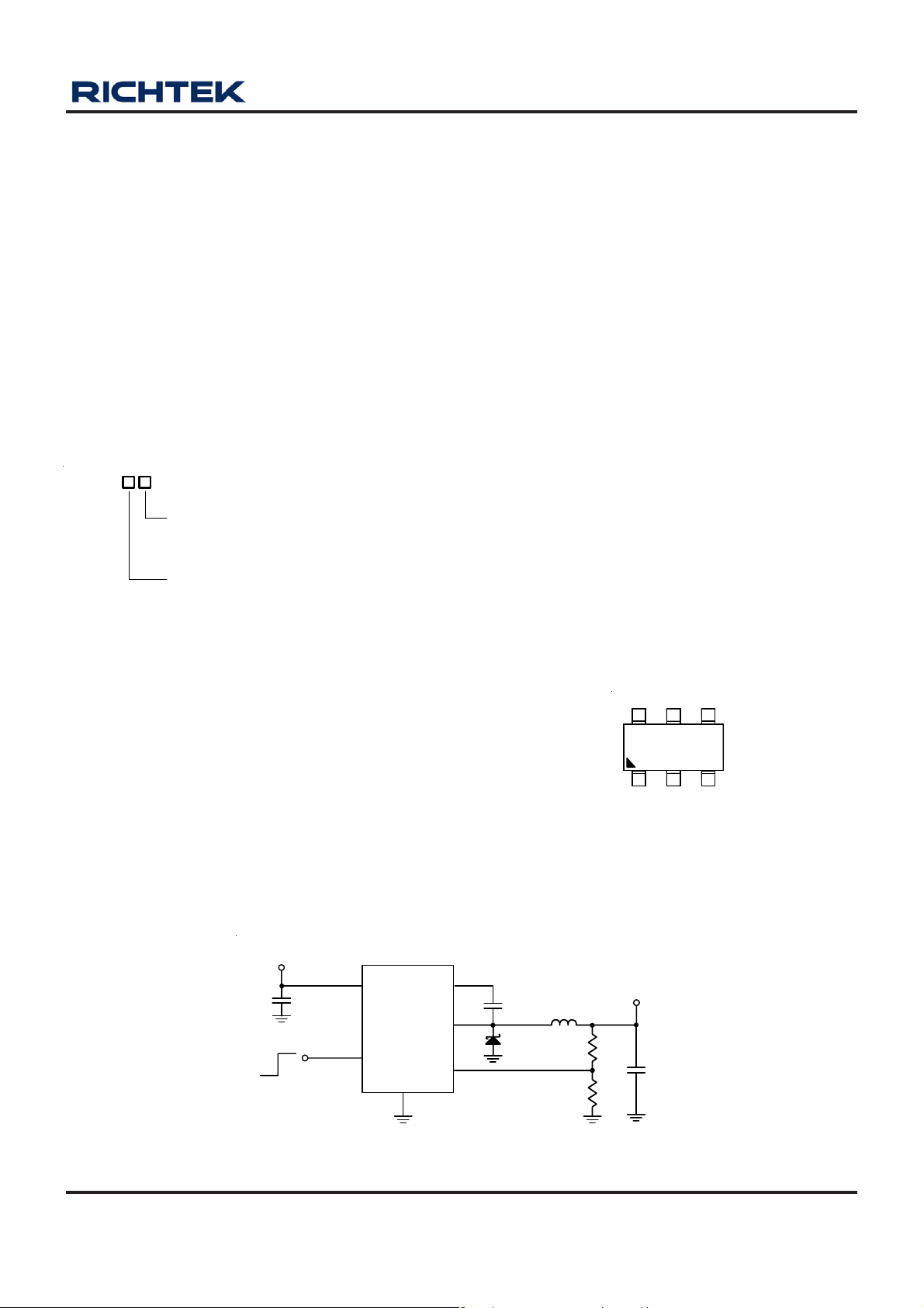
Typical Application Circuit
V
IN
4.5V to 24V
V
R1
62k
R2
19.6k
OUT
3.3V
C2
22µF
C1
10µF
Chip Enabl e
Open =
Automatic Startu p
5
VIN
RT8259
PHASE
4
EN
GND
2
BOOT
FB
1
CB
10nF
6
D1
B230A
3
L1
4.7µH
DS8259-03 March 2011 www.richtek.com
1

RT8259
Table 1. Recommended Component Selection, C2 = 22
V
(V) 1.2 1.8 2.5 3.3 5 8 10 15
OUT
μμ
μF
μμ
L1 (μH) 2 2 3.6 4.7 6.8 10 10 15
R1 (kΩ) 62 62 62 62 62 68 68 68
R2 (kΩ) 124 49.9 29.4 19.6 12 7.5 5.9 3.9
Functional Pin Description
Pin No. P in Nam e Pin Funct io n
Bootstrap. A capacitor is connected between PHASE and BOOT pins to form a floating
1 BOOT
2 GND
3 FB
4 EN
5 VIN
6 PHASE Switch Output.
supply across the power switch driver. This capacitor is needed to drive the power switch‘s
gate abov e the supply voltage .
Ground. This pin is the voltage reference for the regulated output voltage. For this reason,
care must be taken in its layout. This node should be placed outside of the D1 to C1 ground
pa th to pre ven t switching curr ent spikes fr om i n ducing v olta g e noise into the part.
Feedback. An exter nal resistor divide r from the output to GND tapp ed to the FB pin sets the
output vol tag e. The valu e of the divider resisto rs also set loop bandwidth.
Chip Enabl e (Active High). If the EN pin is open, it will be p ulled to high by internal circuit.
Supply Volt age. Byp ass VIN to GND with a suita ble large capacitor to prevent large voltage
spikes from appea ring at the input.
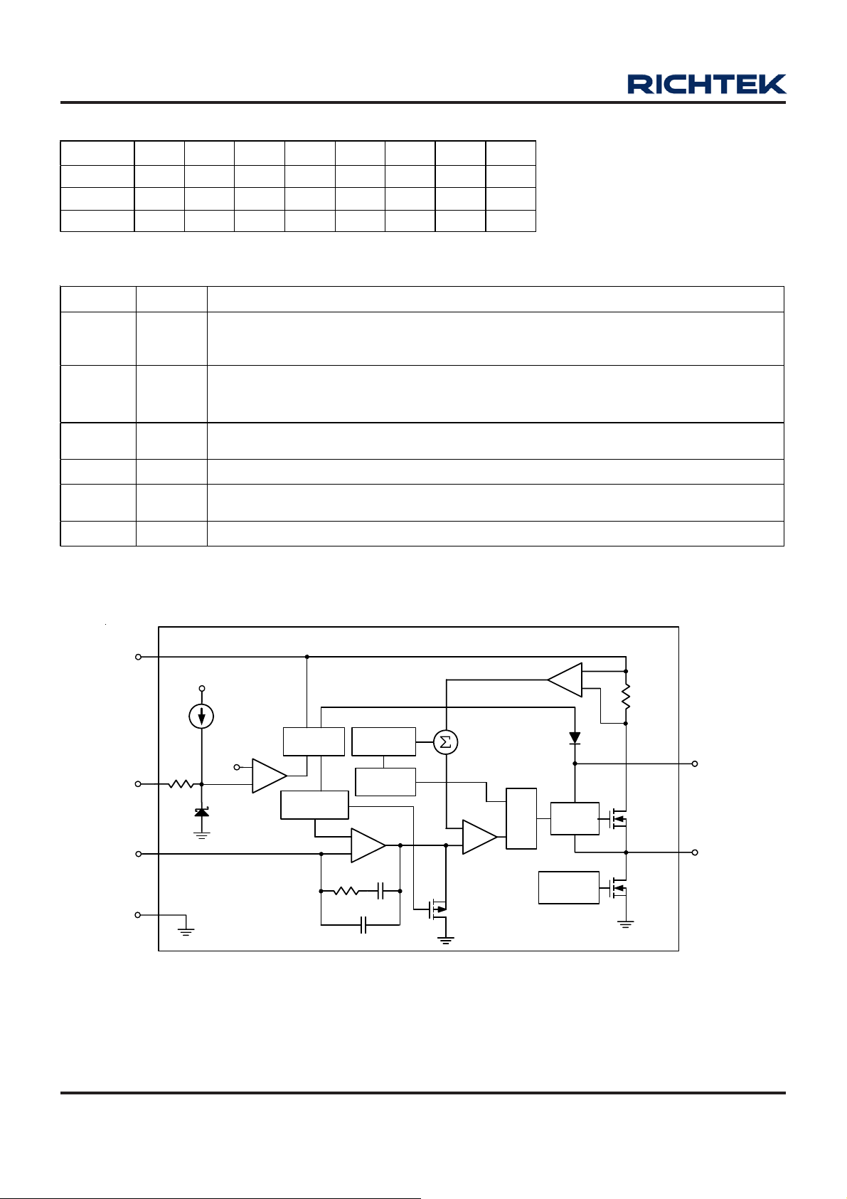
Function Block Diagram
VIN
1µA
+
Shutdown
Comparator
EN
FB
GND
10k
1.1V
3V
Regulator
Reference
400k
Ramp
Generator
Oscillator
1.4MHz
+
EA
30pF
1pF
Current Sense Amp
S
+
PWM
Comparator
OC Limit Clamp
Q
R
X20
Driver
Bootstrap
Control
+
25mΩ
Ω
BOOT
PHASE
DS8259-03 March 2011www.richtek.com
2

Absolute Maximum Ratings (Note 1)
RT8259
z Supply V oltage, V
z PHASE V oltage ----------------------------------------------------------------------------------------------------- −0.3V to (V
z BOOT V oltage ------------------------------------------------------------------------------------------------------- V
z All Other Pins-------------------------------------------------------------------------------------------------------- 0.3V to 6V
z Output V oltage ------------------------------------------------------------------------------------------------------ −0.3V to 15V
z Power Dissipation, P
------------------------------------------------------------------------------------------------ 26V
IN
@ T
D
= 25°C
A
PHASE
+ 6V
+ 0.3V)
IN
T/SOT-23-6 ----------------------------------------------------------------------------------------------------------- 0.4W
z Package Thermal Resistance (Note 2)
T/SOT-23-6, θJA------------------------------------------------------------------------------------------------------ 250°C/W
z Junction T emperature ---------------------------------------------------------------------------------------------- 150°C
z Lead T emperature (Soldering, 10 sec.) ------------------------------------------------------------------------ 260°C
z Storage T emperature Range -------------------------------------------------------------------------------------- −65°C to 150 °C
z ESD Susceptibility (Note 3)
HBM (Human Body Mode)---------------------------------------------------------------------------------------- 2kV
MM (Machine Mode) ----------------------------------------------------------------------------------------------- 200V
Recommended Operating Conditions (Note 4)
z Supply V oltage, V
z Output V oltage, V
z EN Voltage, V
z Junction T emperature Range ------------------------------------------------------------------------------------- −40°C to 125°C
z Ambient T emperature Range ------------------------------------------------------------------------------------- −40°C to 85°C
------------------------------------------------------------------------------------------------ 4.5V to 24V
IN
---------------------------------------------------------------------------------------------- 0.8V to 15V
OUT
----------------------------------------------------------------------------------------------------- 0V to 5.5V
EN
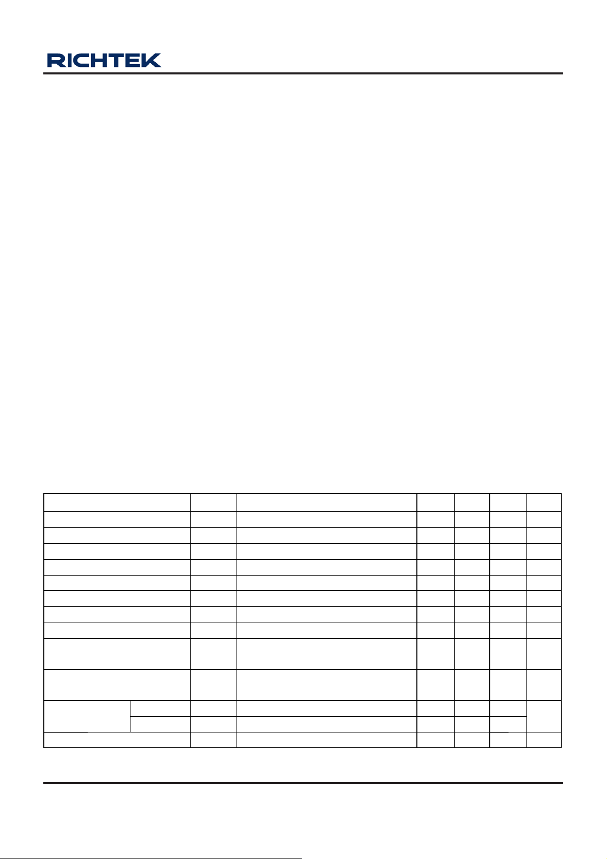
Electrical Characteristics
(VIN = 12V, TA = 25° C unless otherwise specified)
Parameter Symbol Test Conditions Min Typ Max Unit
Feedback Reference Voltage VFB 4.5V ≤ V
Feedback Current IFB VFB = 0.8V -- 0.1 0.3 μA
Switch On Resistance R
Switch Lea kage V
Cur rent Limit I
LIM
-- 0.3 -- Ω
DS(ON)
EN
V
BOOT
Oscillator Frequency fSW 1.2 1.4 1.6 MHz
Maximum Duty Cycle -- 80 -- %
Minimum On-Time tON -- 100 -- ns
Under Voltage Lockout
Threshold
Under Voltage Lockout
Threshold Hysteresis
EN Input Voltage
Logic-High VIH 1.4 -- -Logic-Low V
EN Pull Up Current V
Rising 3.9 4.2 4.5 V
-- 200 -- mV
-- -- 0.4
IL
EN
≤ 24V 0.784 0.8 0.816 V
IN
= 0V, V
− V
PHASE
= 0V -- -- 10 μA
PHASE
= 4.8V 1.6 2.1 -- A
V
= 0V -- 1 -- μA
T o be continued
DS8259-03 March 2011 www.richtek.com
3

RT8259
Parameter Symbol Test Conditions Min Typ Max Unit
Shutdown Current I
Quiescent Current IQ V
SHDN
V
EN
EN
= 0V -- 25 -- μA
= 2V, VFB = 1V (Not Switching) -- 0.55 1 mA
Therma l Shutdown TSD -- 150 -- °C
Note 1. Stresses listed as the above "Absolute Maximum Ratings" may cause permanent damage to the device. These are for
stress ratings. Functional operation of the device at these or any other conditions beyond those indicated in the
operational sections of the specifications is not implied. Exposure to absolute maximum rating conditions for extended
periods may remain possibility to affect device reliability.
Note 2. θ
Note 3. Devices are ESD sensitive. Handling precaution is recommended.
Note 4. The device is not guaranteed to function outside its operating conditions.
is measured in the natural convection at TA = 25°C on a high effective four layers thermal conductivity test board of
JA
JEDEC 51-7 thermal measurement standard.
DS8259-03 March 2011www.richtek.com
4

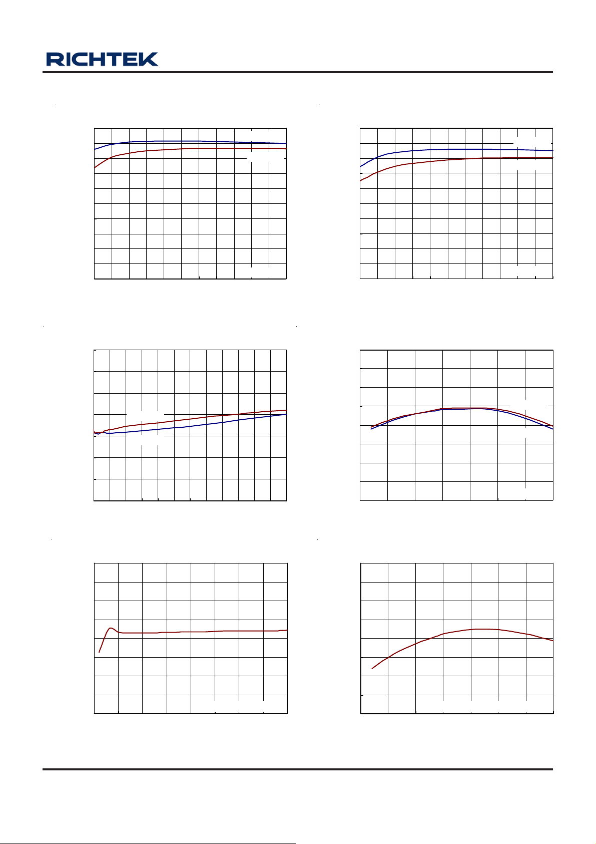
Typical Operating Characteristics
RT8259
Efficiency vs. Load Current
100
90
80
70
60
50
40
Efficiency (%)
30
20
10
0
0.1 0.2 0.3 0.4 0.5 0.6 0.7 0.8 0.9 1 1.1 1.2
Load C ur rent (A)
Output Voltage vs. Load Current
3.333
3.328
3.323
Output Vol t ag e (V)
3.318
3.313
3.308
3.303
3.298
0 0.1 0.2 0.3 0.4 0.5 0.6 0.7 0.8 0.9 1 1.1 1.2
VIN = 24V
VIN = 12V
Load C ur ren t ( A)
VIN = 12V
VIN = 24V
V
= 5V
OUT
Efficiency vs. Load Current
100
90
80
70
60
50
40
Efficiency (%)
30
20
10
0
0.1 0.2 0.3 0.4 0.5 0.6 0.7 0.8 0.9 1 1.1 1.2
Load Current (A)
Output Voltage vs. Temperature
3.38
3.36
3.34
3.32
3.30
3.28
Output Vol tage ( V)
3.26
3.24
3.22
-50 -25 0 25 50 75 100 125
Temper at ur e (°C)
VIN = 12V
VIN = 24V
V
= 3.3V
OUT
VIN = 24V
VIN = 12V
I
OUT
= 0A
Frequency vs. Input Voltage
1.55
1.50
1.45
1.40
1.35
1.30
Frequency (MHz)
1.25
1.20
V
= 3.3V, I
1.15
4 6.5 9 11.51416.51921.524
Input Vol tage (V)
OUT
OUT
= 0.3A
1.55
1.50
1.45
1.40
1.35
1.30
Frequenc y (MHz) 1
1.25
1.20
1.15
-50 -25 0 25 50 75 100 125
Frequency vs. Temperature
VIN = 12V, V
Temperature (°C)
= 3.3V, I
OUT
OUT
= 0.3A
DS8259-03 March 2011 www.richtek.com
5
 Loading...