

®
RT8237C/D
High Efficiency Single Synchronous Buck PWM Controller
General Description
The RT8237C/D PWM controller provides high efficiency ,
excellent transient response, a nd high DC output a ccuracy
needed for stepping down high voltage batteries to
generate low voltage CPU core, I/O, and chipset RAM
supplies in notebook computers.
The constant on-time PWM control scheme ha ndles wide
input/output voltage ratios with ea se and provides 100ns
“instant-on” response to load transients while maintaining
a relatively constant switching frequency .
The RT8237C/D achieves high efficiency at a reduced cost
by eliminating the current sense resistor found in
traditional current mode PWMs. Efficiency is further
enhanced by its ability to drive very large synchronous
rectifier MOSFETs and enter diode emulation mode at
light load condition. The buck conversion allows this device
to directly step down high voltage batteries at the highest
possible efficiency. The pre-set frequency selections
minimize design effort required for new designs. The
RT8237C/D is intended for CPU core, chipset, DRAM, or
other low voltage supplies a s low a s 0.7V . The RT8237C
is available in a W DF N-10L 3x3 package, The R T8237D is
available in a WQFN-12L 2x2 package.
Features
Wide Input Voltage Range : 4.5V to 26V
Output Voltage Range : 0.7V to 3.3V
Built-in 0.5% 0.7V Reference Voltage
Quick Load-Step Response within 100ns
4700ppm/
Side R
4 Selectable Frequency Setting
Soft-Start Control
Drives Large Synchronous-Rectifier FET s
Integrated Boot Switch
Built-in OVP/OCP/UVP
Thermal Shutdown
Power Good Indicator
RoHS Compliant and Halogen Free
°°
°C Programmable Current Limit by Low
°°
Sensing
DS(ON)
Applications
Notebook Computers
CPU Core Supply
Chipset/RAM Supply a s Low as 0.7V
Generic DC/DC Power Regulator
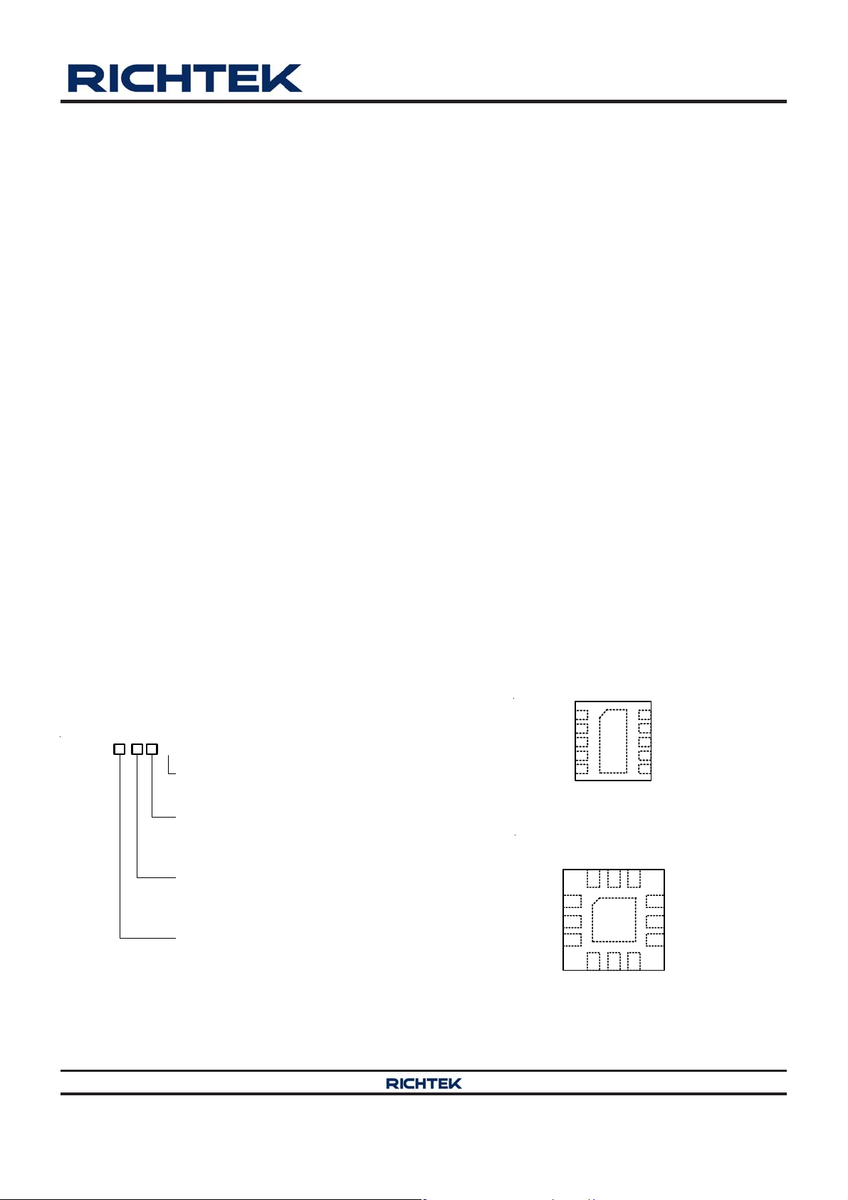
Pin Configurations
(TOP VIEW)
GND
11
10
9
8
7
6
BOOT
UGATE
PHASE
VCC
LGATE
Ordering Information
RT8237
(2)
Pin 1 Orientation
(2) : Quadrant 2, Follow EIA-481-D
Package Type
PGOOD
CS
EN
FB
RF
1
2
3
4
5
WDFN-10L 3x3
RT8237C
QW : WDFN-10L 3x3 (W-Type)
QW : WQFN-12L 2x2 (W-Type)
Lead Plating System
Z : ECO (Ecological Element with
Halogen Free and Pb free)
C : WDFN-10L 3x3
LGATE FB
VCC
PHASE
D : WQFN-12L 2x2
Note :
Richtek products are :
RoHS compliant and compatible with the current require-
ments of IPC/JEDEC J-STD-020.
Suitable for use in SnPb or Pb-free soldering processes.
Copyright 2014 Richtek Technology Corporation. All rights reserved. is a registered trademark of Richtek Technology Corporation.
DS8237C/D-06 February 2014 www.richtek.com
©
GNDNCRF
12 1011
1
GND
2
3
13
BOOT
UGATE
654
PGOOD
WQFN-12L 2x2
RT8237D
9
8
EN
7
CS
1
RT8237C/D
Marking Information
RT8237CZQW
Z3 : Product Code
Z3 YM
DNN
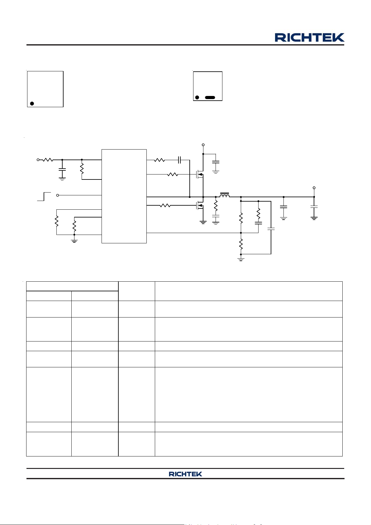
Typical Application Circuit
R1
V
0
CC
Chip Enable
YMDNN : Date Code
C1
R5
1µF
100k
16V
R
RF
R
470k
:
*
OC_SET
30k
l
a
n
i
o
t
p
O
V
P
EN
RF
C
G
R
T
3
8
2
7
C
/
C
C
O
G
S
D
N
B
U
G
D
O
P
H
L
RT8237DZQW
72 : Product Code
72W
V
C
BOOT
0
R
LGATE
R
UGATE
0
0.1µF
50V
0
R
D
O
A
A
G
BOOT
O
T
T
E
S
E
A
T
E
F
B
IN
W : Date Code
C2
10µF x 3
50V
L
OUT
0.45µH
R2*
C3*
R
FB1
5.1k
R
FB2
10k
R3*
C4*
V
OUT
1.05V
C6
10µF x 2
16V
C5*
C
OUT
330µF x 2
16V
Functional Pin Description
Pin No.
RT8237C RT8237D
1 6 PGOOD
2 7 CS
3 8 EN PWM Enable. Pull low to GND to disable the PWM.
4 9 FB
5 10 RF
6 1 LGATE Gate Drive Output for Low S ide External MOSFET.
7 2 VCC
Pin Name Pi n Func t i o n
Open Drain Power Good Indicator. High impedance indicates
power is good.
Curren t Li mit Thr eshold Setting I nput . Connect a setti ng r esi stor to
GND and the current limit threshold is equal to 1/8 of the volt age
at this pin.
Feedback Input. Connect FB to a resistor voltage divider
V
OUT
fro m V
to GND to adjust the output from 0.7V to 3.3V
OUT
Switching Frequency Selection. Connect a resistance to select
switching frequency as shown in Electrical Charac t er istics.
The swi t c hin g frequency is det ect ed and latched af ter start up. This
pin also cont rols Diode emulat ion mode or forced C CM selection.
Pull down to GND with resistor : Diode Emulation Mode.
Connect to PGOOD with resistor : forced CCM after PGOOD
becomes hi gh.
Contr ol Voltage Input. This pin provides the power for the buck
contr oller, the low si de dr iv er an d th e bootstrap ci rcuit for high side
dri v er. Byp ass to GND wi th a 1F ceramic capa citor.
Copyright 2014 Richtek Technology Corporation. All rights reserved. is a registered trademark of Richtek Technology Corporation.
©
DS8237C/D-06 February 2014www.richtek.com
2
RT8237C/D
Pin No.
Pin Name Pi n Func t i o n
RT8237C RT8237D
8 3 PHASE
9 4 UGATE Gate Drive Output for High Side Exter nal MOSFET.
10 5 BOOT
--- 11 NC No Internal Connection.
11
(Expo sed Pad)
12, 13
(Exp osed Pad)
GND
Function Block Diagram
TRIG
RF
PHASE
On-time
Compute
1-SHOT
External Inductor C onnection Pin for PWM Converter. It behaves
as the current sense comparator input for low side MOSFET
R
sensing and r eference voltage for on time generation.
DS(ON)
Supply Input for High Si de Driver. Connect through a capacitor to
the float ing node (PHASE) pin.
Ground. The exposed pad must be soldered to a large PCB and
conn ect ed to GND for maxim um power dissipation.
VCC
COMP
+
R
QS
PWM
DRV
BOOT
UGATE
FB
VCC
EN
CS
POR
10µA
125%
V
REF
70%
V
REF
Timer
SS
+
-
+
-
V
REF
OV
UV
125% V
90% V
Latch
S1 Q
Latch
S1 Q
-
REF
+
+
REF
Thermal
Shutdown
Min. t
OFF
QTRIG
1-SHOT
DEM/FCCM
+
X(1/8)
+
-
X(-1/8)
DRV
PHASE
LGATE
GND
PGOOD
Copyright 2014 Richtek Technology Corporation. All rights reserved. is a registered trademark of Richtek Technology Corporation.
©
DS8237C/D-06 February 2014 www.richtek.com
3
RT8237C/D
Absolute Maximum Ratings (Note 1)
VCC, FB, PGOOD, EN, CS, RF to GND ---------------------------------------------------------------------------- −0.3V to 6V
BOOT to PHASE ---------------------------------------------------------------------------------------------------------- −0.3V to 6V
PHASE to GND
DC----------------------------------------------------------------------------------------------------------------------------- −0.3V to 32V
<20ns ------------------------------------------------------------------------------------------------------------------------ −8V to 38V
UGA TE to PHASE -------------------------------------------------------------------------------------------------------- −0.3V to 6V
DC----------------------------------------------------------------------------------------------------------------------------- −0.3V to 6V
<20ns ------------------------------------------------------------------------------------------------------------------------ −5V to 7.5V
LGA TE to GN D ------------------------------------------------------------------------------------------------------------- −0.3V to 6V
DC----------------------------------------------------------------------------------------------------------------------------- −0.3V to 6V
<20ns ------------------------------------------------------------------------------------------------------------------------ −2.5V to 7.5V
Power Dissipation, P
W D FN-10L 3x3------------------------------------------------------------------------------------------------------------- 0.952W
WQFN-12L 2x2 ------------------------------------------------------------------------------------------------------------ 0.606W
Package Thermal Re sistance (Note 2)
W DFN-10L 3x3, θJA------------------------------------------------------------------------------------------------------- 105°C/W
WDFN-10L 3x3, θJC------------------------------------------------------------------------------------------------------- 8.2°C/W
WQFN-12L 2x2, θJA------------------------------------------------------------------------------------------------------- 165°C/W
Lead Temperature (Soldering, 10 sec.)------------------------------------------------------------------------------- 260°C
Junction T emperature----------------------------------------------------------------------------------------------------- 150°C
Storage T emperature Range -------------------------------------------------------------------------------------------- −65°C to 150°C
ESD Susceptibility (Note 3)
HBM (Human Body Model)---------------------------------------------------------------------------------------------- 2kV
MM (Machine Model) ----------------------------------------------------------------------------------------------------- 200V
@ TA = 25°C
D
Recommended Operating Conditions (Note 4)
Input Voltage, V
Control Voltage, V
Junction T emperature Range-------------------------------------------------------------------------------------------- −40°C to 125°C
Ambient T emperature Range-------------------------------------------------------------------------------------------- −40°C to 85°C
---------------------------------------------------------------------------------------------------------- 4.5V to 26V
IN
------------------------------------------------------------------------------------------------------ 4.5V to 5.5V
CC
Electrical Characteristics
(VCC = 5V, T
Input Power Supply
VCC Quiescent Supply
Current
VCC Shutdown Current I
CS Shutdown Curr ent CS pull to GND -- -- 1 A
FB Error Co mp arator
Threshold
FB Input Bias Current V
Copyright 2014 Richtek Technology Corporation. All rights reserved. is a registered trademark of Richtek Technology Corporation.
4
= 25°C, unless otherwise specified)
A
Parameter Symbol Test Conditions Min Typ Max Unit
I
Q
SHDN
FB forced above the regulation
point, V
= 5V,
EN
VCC current, VEN = 0V -- -- 1 A
-- 500 1250 A
DEM 0.7005 0.704 0.7075
V
REF
©
DEM, TA = 40 to 85C (Note 5) 0.697 0.704 0.711
= 0.735V 1 0.01 1 A
FB
DS8237C/D-06 February 2014www.richtek.com
V

RT8237C/D
Parameter Symbol Test Conditions Min Typ Max Unit
V
Voltage Range 0.7 -- 3.3 V
OUT
RRF = 470k (Note 6) -- 290 --
Switc hing Fre quen cy f
SW
Minimum Off-Time 250 400 550 ns
Current Sensing
CS Source Current ICS 9 10 11 A
CS Source Current TC -- 4700 -- ppm/C
Zero Crossing Thresho ld DEM 10 -- 5 mV
Cu rrent Lim it T hr eshol d V
LIMIT
PHASE GND, VCS = 2.4V -- 300 --
Negative Current Limit
Threshold
PHASE GND, VCS = 1.6V -- 200 - PHASE GND, V
Protection Function
Output UV Threshold
OVP Threshold
OV Fault Delay FB forc ed above OV threshold -- 5 -- s
VCC Under Voltage Lockout
Threshold
V
Soft-Start From EN = high to V
OUT
UVLO
UV Blank Time From EN signal going high -- 3 -- ms
Ther mal Shut dow n TSD -- 150 -- C
Driver On Resistance
UGATE Drive Source R
UGATE Drive Sink R
LGATE Drive Source R
LGATE Drive Sink R
Dead Time
UGATEsr
UGATEsk
LGATEsr
LGATEsk
LGATE R ising (V
UGATE Rising -- 30 --
Internal Boost Charging Switch
On Resistance
VCC to BOOT, 10 mA -- -- 8 0
EN Threshold
EN Input
Threshold Voltage
Logic-High VIH 1.8 -- -Logic-Low V
-- -- 0.5
IL
RRF = 200k (Note 6) -- 340 --
kHz
RRF = 100k (Note 6) -- 380 -RRF = 39k (Note 6) -- 430 --
GND PHASE, V
GND PHASE, VCS = 1.6V 185 200 215
= 2.4V 280 300 320
CS
mV
GND PHASE, VCS = 0.4V 40 50 60
mV
= 0.4V -- 50 --
CS
With respect to error
comparator threshold
With respect to error
comparator threshold
65 70 75 %
120 125 130 %
Falling edge,
hysteresis = 100mV, PWM
3.7 3.9 4.1 V
disabled below this level
= 95% -- 1300 -- s
OUT
BOOT PHASE forced to 5V -- 1.8 3.6
BOOT PHA SE forced to 5V -- 1.2 2.4
LG ATE, High State -- 1.8 3.6
LGATE, Low State -- 0.8 1.6
= 1.5V) -- 30 --
PHASE
ns
V
Copyright 2014 Richtek Technology Corporation. All rights reserved. is a registered trademark of Richtek Technology Corporation.
DS8237C/D-06 February 2014 www.richtek.com
©
5
RT8237C/D
Parameter Symbol Test Conditions Min Typ Max Unit
Mode Decision
VRF Threshold for DEM -- -- 0.5 V
VRF Threshold for FCCM 1.8 -- -- V
PGOOD
Tr ip Thres ho ld (fa lli ng,
leaving PGOOD)
Trip Threshold (rising,
leaving PGOOD)
Fault Propagation Delay
Output Low Voltage I
Leakage Current High State, forced to 5V -- -- 1 A
Note 1. Stresses beyond those listed “Absolute Maximum Ratings” may cause permanent damage to the device. These are
stress ratings only, and functional operation of the device at these or any other conditions beyond those indicated in
the operational sections of the specifications is not implied. Exposure to absolute maximum rating conditions may
affect device reliability.
Note 2. θ
Note 3. Devices are ESD sensitive. Handling precaution is recommended.
Note 4. The device is not guaranteed to function outside its operating conditions.
Note 5. Guaranteed by design. Not production tested.
Note 6. Not production tested. Test condition is V
is measured at T
JA
measured at the exposed pad of the package.
= 25°C on a low effective thermal conductivity single-layer test board per JEDEC 51-3. θJC is
A
Measured at FB, with respect to
referenc e, Hysteresis = 3%
Measured at FB, with respect to
reference,
Hys teresis = 3%
Falling Edge, FB forced below
PGOOD trip threshold
= 1m A -- -- 0.4 V
SINK
= 8V, V
IN
= 1.1V, I
OUT
= 10A using application circuit.
OUT
87 90 93 %
120 125 130 %
-- 2.5 -- s
Copyright 2014 Richtek Technology Corporation. All rights reserved. is a registered trademark of Richtek Technology Corporation.
6
©
DS8237C/D-06 February 2014www.richtek.com

Typical Operating Characteristics
RT8237C/D
Efficiency vs. Load Current
100
90
80
70
60
50
40
Efficiency (% )
30
20
10
0
0.001 0.01 0.1 1 10 100
DEM
V
IN
CCM
= 8V, V
= 1.05V, R
OUT
= 470kΩ
RF
Load Current (A)
Efficiency vs. Load Current
100
90
80
70
60
50
40
Efficiency (% )
30
20
10
0
0.001 0.01 0.1 1 10 100
DEM
V
= 20V , V
IN
Load Current (A)
CCM
= 1.05V, R
OUT
= 470kΩ
RF
Efficiency vs. Load Current
100
90
80
70
60
50
40
Efficiency (% )
30
20
10
0
0.001 0.01 0.1 1 10 100
DEM
V
= 12V , V
IN
CCM
= 1.05V, R
OUT
RF
Load Curren t (A)
Switching Frequency vs. Load Current
1000
100
10
1
Switching Frequency (kHz) 1
0.1
0.001 0.01 0.1 1 10 100
CCM
V
IN
Load Current (A)
DEM
= 12V , V
= 1.05V, R
OUT
RF
= 470kΩ
= 470kΩ
Switching Frequency vs . Loa d Current
1000
CCM
100
10
DEM
1
Switching Frequency (kHz) 1
V
= 12V , V
0.1
0.001 0.01 0.1 1 10 100
IN
= 1.05V, R
OUT
= 200kΩ
RF
Load Current (A)
Copyright 2014 Richtek Technology Corporation. All rights reserved. is a registered trademark of Richtek Technology Corporation.
©
Swit ching Frequency (kHz) 1
Switching Frequency vs. Load Current
1000
CCM
100
10
DEM
1
V
= 12V , V
0.1
0.001 0.01 0.1 1 10 100
IN
Load Curren t (A)
= 1.05V, R
OUT
= 100kΩ
RF
DS8237C/D-06 February 2014 www.richtek.com
7

RT8237C/D
)
)
Switching Frequency vs. Load Current
1000
CCM
100
10
DEM
1
Swit ching Frequency (kHz) 1
V
= 12V, V
0.1
0.001 0.01 0.1 1 10 100
IN
= 1.05V, R
OUT
Load Current (A)
Line Regulation vs. Tem pe rature
1.0
DEM
0.8
0.6
0.4
0.2
0.0
-0.2
-0.4
Line Regulation (%
-0.6
-0.8
-1.0
V
= 12V, V
IN
-50 -25 0 25 50 75 100 125
= 1.05V, R
OUT
= 470kΩ, No Load
RF
Temperature (C)
RF
= 39kΩ
Load Regulation vs. Temperature
1.0
CCM
0.8
0.6
0.4
0.2
0.0
-0.2
-0.4
Load Regulat ion (%
-0.6
-0.8
-1.0
V
= 12V, V
IN
-50 -25 0 25 50 75 100 125
OUT
= 1.05V, I
OUT
= 10A, R
Temperatur e (C)
Switching Frequency vs . Input Voltage
500
475
450
425
400
375
350
325
300
275
250
Switching Frequency (kHz) 1
225
200
4 6 8 10 12 14 16 18 20 22 24 26
RRF = 39k
RRF = 100k
RRF = 200k
RRF = 470k
Input Voltage (V)
= 470kΩ
RF
I
OUT
= 10A
CS Source Current vs. Temperature
20
18
16
14
12
10
8
6
4
CS Source Current (µA)
2
0
-50 -25 0 25 50 75 100 125
V
CC
= 5V
V
OUT
(50mV/Div)
I
OUT
(10A/Div)
UGATE
(20V/Div)
LGATE
(5V/Div)
Load Transient Response
VIN = 12V, I
= 0A to 20A, V
OUT
Time (40μs/Div)
OUT
= 1.05V
Temperature (C)
Copyright 2014 Richtek Technology Corporation. All rights reserved. is a registered trademark of Richtek Technology Corporation.
©
DS8237C/D-06 February 2014www.richtek.com
8

RT8237C/D
V
OUT
(500mV/Div)
LGATE
(5V/Div)
PGOOD
(5V/Div)
EN
(5V/Div)
V
OUT
(500mV/Div)
PGOOD
(5V/Div)
OVP
DEM, VIN = 12V, No Load
Time (40μs/Div)
Power On from EN
V
OUT
(1V/Div)
PGOOD
(5V/Div)
UGATE
(20V/Div)
LGATE
(5V/Div)
EN
(5V/Div)
V
OUT
(500mV/Div)
PGOOD
(5V/Div)
UVP
VIN = 12V, V
Time (40μs/Div)
Power On from EN
OUT
= 1.05V
UGATE
(10V/Div)
DEM, VIN = 12V, No Load
Time (1ms/Div)
UGATE
(10V/Div)
CCM, VIN = 12V, No Load
Time (1ms/Div)
Copyright 2014 Richtek Technology Corporation. All rights reserved. is a registered trademark of Richtek Technology Corporation.
©
DS8237C/D-06 February 2014 www.richtek.com
9

RT8237C/D
Application Information
The RT8237C/D PWM controller provides high efficiency ,
excellent transient response, a nd high DC output a ccuracy
needed for stepping down high voltage batteries to
generate low voltage CPU core, I/O, and chipset RAM
supplies in notebook computers. Richtek Mach
ResponseTM technology is specifically designed for
providing 100ns“instant-on” response to load steps while
maintaining a relatively constant operating frequency a nd
inductor operating point over a wide range of input voltages.
The topology circumvents the poor load transient timing
problems of fixed frequency current mode PWMs, while
avoiding the problems caused by widely varying switching
frequencies in conventional constant on-ti me and consta nt
off-time PWM schemes. The DRVTM mode PWM
modulator is specifically designed to have better noise
immunity for such a single output application.
PWM Operation
The Mach ResponseTM DRVTM mode controller relies on
the output filter capacitor's effective series resistance
(ESR) to act as a current sense resistor, so the output
ripple voltage provides the PWM ra mp signal. Referring to
the function block diagra m, the synchronous UGATE driver
is turned on at the beginning of each cycle. After the
internal one-shot timer expires, the UGA TE driver will be
turned off. The pulse width of this one shot is determined
by the converter's input voltage and the output voltage to
keep the frequency fairly constant over the input voltage
range. Another one-shot sets a minimum off-ti me (400ns
typ.).
On-Time Control (TON/MODE)
The on-time one-shot comparator has two inputs. One
input monitors the output voltage from the PHASE pin,
while the other input sa mples the input voltage and converts
it to a current. This input voltage proportional current is
used to charge an internal on-time ca pa citor . The on-time
is the time required for the voltage on this capacitor to
charge from zero volts to V
, thereby making the on-
OUT
time of the high side switch directly proportional to output
voltage and inversely proportional to input voltage.
The on-time is given by :
tON = (V
OUT
/ VIN) / f
SW
Table 1. RF Connection and Switching Frequency
RRF (k) Switching Frequency (kHz)
470k 290
200k 340
100k 380
39k 430
Note : For DEM, connect RRF to GND; for CCM, connect
to PGOOD.
R
RF
Enable and Disable
The EN pin allows for power sequencing between the
controller bias voltage and another voltage rail. The
RT8237C/D remains in shutdown if the EN pin is lower
than 500mV. When the EN pin rises above the VEN trip
point, the RT8237C/D will begin a new initialization and
soft-start cycle.
POR, UVLO and Soft-Start
Power-on reset (POR) occurs when VCC rises above
approximately 4.1V, in which the RT8237C/D resets the
fault latch and prepares the PWM for operation. Below
3.7V (min), the VCC Under Voltage Lockout (UVLO)
circuitry inhibits switching by keeping UGA TE and LGA TE
low. A built-in soft-start is used to prevent the power supply
input from surge currents after PWM is enabled. A ramping
up current limit threshold eliminates the V
folded-back
OUT
current during the soft-start duration.
Mode Selection (RF) Operation
T o select the operation mode, connect a resistor from the
RF pin to either GND or PGOOD. When the resistor is
connected to GND, the controller operates in diode
emulation mode. When the resistor is connected to
PGOOD, the controller operates in CCM mode.
Diode-Emulation Mode (RRF Connected to GND)
In diode-emulation mode, the RT8237C/D automatically
reduces switching frequency at light load conditions to
maintain high efficiency. This reduction of frequency is
achieved smoothly without increa sing V
ripple or load
OUT
regulation. As the output current decreases from heavy
load condition, the inductor current is reduced and
eventually comes to the point where its valley touches
Copyright 2014 Richtek Technology Corporation. All rights reserved. is a registered trademark of Richtek Technology Corporation.
10
©
DS8237C/D-06 February 2014www.richtek.com

RT8237C/D
zero current, which is the boundary between continuous
conduction and discontinuous conduction modes. By
emulating the behavior of diodes, the low side MOSFET
allows only partial negative current to flow when the
inductor freewheeling current reaches negative. As the load
current is further decrea sed, it takes longer a nd longer to
discharge the output capacitor to the level that requires
the next “ON” cycle. The on-time is kept the same as
that in heavy load condition. On the contrary, when the
output current increa ses from light load to heavy load, the
switching frequency increa ses to the preset value as the
inductor current reaches the continuous condition. This
is shown in Figure 1. The tran sition load point to the light
load operation is calculated a s follows :
VV
IN OUT
It
LOAD ON
where t
I
L
0
2L
is the on-time.
ON
Slope = (VIN -V
t
ON
OUT
) / L
I
L, PEAK
I
LOAD
t
= I
L, PEAK
/ 2
Figure 1. Boundary Condition of CCM/DCM
The switching waveforms may appear noisy and
asynchronous when light loa ding causes diode-emulation
operation, but this is a normal operating condition that
results in high light load efficiency . T rade-offs in DEM noise
vs. light load efficiency is made by varying the inductor
value. Generally, low inductor values produce a broader
efficiency vs. load curve, while higher values result in higher
full load efficiency (assuming that the coil resistance
remains fixed) and less output voltage ripple. The
disadvantages for using higher inductor values include
larger physical size and degraded load tra nsient response
(especially at low input voltage levels).
Forced-CCM Mode (FCCM)
The low noise, forced-CCM mode disables the zerocrossing comparator, which controls the low side switch
on-time. This causes the low side gate drive waveform to
become the complement of the high side gate drive
waveform. This in turn causes the inductor current to
reverse at light loads as the PWM loop to maintain duty
ratio V
OUT/VIN
. A fairly constant switching frequency is
the benefit of forced-CCM mode, but this comes at a cost.
The no load battery current can be up to 10mA to 40mA,
depending on the external MOSFETs.
Current Limit Setting (CS)
The RT8237C/D has a cycle-by-cycle current limiting
control. The current limit circuit employs a unique “valley”
current sensing algorithm. If the magnitude of the current
sense signal at PHASE is above the current limit
threshold, the PWM is not allowed to initiate a new cycle
(see Figure 2). In order to provide both good accura cy and
a cost effective solution, the RT8237C/D supports
temperature compensated MOSFET R
DS(ON)
sensing.
The CS pin of the RT8237C/D is a multiplexed pin for
PWM enable/disable control and current limit threshold
setting. Connect a setting resistor from this pin to GND
via an N-MOSFET. When the N-MOSFET is turned off, the
PWM is disabled. When the N-MOSFET is turned on, the
PWM is enabled and the current limit threshold is equal
to 1/8 of the voltage at this pin.
Choose a current limit resistor by following below equation:
I
RIPPLE
2
R
OC_SET
I8R
LOAD_OC DS(ON)
V
CS_OC
II
CS CS
Inductor current is monitored by the voltage between the
GND pin and the PHASE pin, so the PHASE pin should
be connected to the drain terminal of the low side
MOSFET . ICS has a temperature coef ficient to compensate
the temperature dependency of the R
. GND is used
DS(ON)
a s the positive current sensing node, so GND should be
connected to the source terminal of the low side MOSFET .
As the comparison is being done during the OFF state,
V
(current limit threshold) sets the valley level of the
LIMIT
inductor current. Thus, the load current at over current
threshold, I
I = +
LOAD_OC
LOAD_OC
= +
, can be calculated as follows :
V
CS_OC
8R 2
DS(ON)
V
CS_OC
8R 2Lf V
DS(ON) IN
I
RIPPLE
1
(V V ) V
IN OUT OUT
Copyright 2014 Richtek Technology Corporation. All rights reserved. is a registered trademark of Richtek Technology Corporation.
DS8237C/D-06 February 2014 www.richtek.com
©
11

RT8237C/D
In an over current condition, the current to the load exceeds
the current to the output capa citor . Thus, the output voltage
falls and eventually crosses the under voltage protection
threshold, inducing IC shutdown.
I
L
I
L, PEAK
BOOT
UGATE
PHASE
V
IN
R
I
LOAD_OC
I
LIMIT
0
t
Figure 2. “Valley” Current Limit
When the device is operating in the FCCM, the negative
current limit protects the external component. The negative
current limit detect threshold is set a s the same value as
positive current limit but negative polarity . The threshold
still is the valley value of the inductor current.
MOSFET Gate Driver
The high side driver is designed to drive high current, low
R
N-MOSFET(s). When configured as a floating
DS(ON)
driver, 5V bi a s voltage is delivered from the VCC supply .
The average drive current is proportional to the gate charge
at VGS = 5V times switching frequency . The insta ntaneous
drive current is supplied by the flying capacitor between
the BOOT and PHASE pins. To prevent shoot through, a
dead time is internally generated between high side
MOSFET off to low side MOSFET on, and low side
MOSFET off to high side MOSFET on. The low side driver
is designed to drive high current, low R
DS(ON)
N-MOSFET(s). The internal pull-down tran sistor that drives
LGATE low is robust, with a 0.5 Ω typical on-resistance.
A 5V bias voltage is delivered from the VCC supply . The
instantaneous drive current is supplied by the flying
cap acitor between VCC a nd GND.
For high current applications, certain combin ations of high
and low side MOSFETs may cause excessive gate-drain
coupling, which can lead to efficiency-killing, EMIproducing shoot-through currents. This is often remedied
by adding a resistor in series with BOOT , which increa ses
the turn-on time of the high side MOSFET without degrading
the turn-off time (see Figure 3).
Figure 3. Reducing the UGA TE Rise T ime
Power Good Output (PGOOD)
The power good output is an open-drain output and requires
a pull-up resistor. When the output voltage is 20% a bove
or 10% below its set voltage, PGOOD gets pulled low. It
is held low until the output voltage returns to within these
tolerances once more. During soft-start, PGOOD is a ctively
held low and is allowed to tra nsition high only after softstart is over and the output rea ches 90% of its set voltage.
There is a 2.5μs delay built into the PGOOD circuitry to
prevent false transitions.
Output Over Voltage Protection (OVP)
The output voltage is continuously monitored for over
voltage protection. When the output voltage exceeds 25%
of its set voltage threshold, over voltage protection is
triggered and the low side MOSFET is latched on. This
activates the low side MOSFET to discharge the output
capacitor. The RT8237C/D is latched once OVP is
triggered and ca n only be released by VCC or EN power
on reset. There is a 5μs delay built into the over voltage
protection circuit to prevent false transition s.
Output Under Voltage Protection (UVP)
The output voltage can be continuously monitored for under
voltage protection. When the output voltage is less than
70% of its set voltage threshold, under voltage protection
is triggered and then both UGA TE and LGA TE gate drivers
are forced low . There is a 2.5μs delay built into the under
voltage protection circuit to prevent false transitions. During
soft-start, the UVP blanking time is 3ms.
Thermal Shutdown (OTP)
The device implements an intern al thermal shutdown to
protect itself if junction temperature exceeds 150°C. When
the junction temperature exceeds the thermal shutdown
threshold that the OTP function will be triggered and the
Copyright 2014 Richtek Technology Corporation. All rights reserved. is a registered trademark of Richtek Technology Corporation.
12
©
DS8237C/D-06 February 2014www.richtek.com

RT8237C/D
RT8237C/D will shut down a nd entry Latch-Off Mode. In
Latch-Off Mode, the RT8237C/D can be reset by EN or
power input VCC.
Output V oltage Setting (FB)
The output voltage can be adjusted from 0.7V to 3.3V by
setting the feedback resistors, R1 a nd R2 (see Figure 4).
Choose R2 to be approximately 10k Ω and solve for R1
using the equation below :
R1
V = V 1+
OUT REF
where V
REF
Figure 4. Setting V
R2
is 0.704V (typ.).
V
OUT
R1
R2
with a Resistive V oltage Divider
OUT
FB
Inductor Selection
The inductor plays an important role in step-down
converters because it stores the energy from the input
power rail and then relea ses the energy to the load. From
the viewpoint of efficiency , the dc resistance (DCR) of the
inductor should be as small as possible to minimize the
conduction loss. In addition, because the inductor takes
up a significant portion of the board spa ce, its size is also
important. Low profile inductors can save board space
especially when there is a height limitation. However , low
DCR and low profile inductors are usually cost ineff ective.
Additionally, larger inductance results in lower ripple
current, which means lower power loss. However, the
inductor current rising time increa ses with inductance value.
This means the tra nsient response will be slower. Therefore,
the inductor design is a compromise between
performance, size a nd cost.
In general, the inductance is designed such that the ripple
current ranges between 20% to 40% of the full load current.
The inductance can be calculated using the following
equation :
VV V
L
MIN
IN OUT OUT
fkI V
SW OUT_rated IN
where k is the ratio between inductor ripple current and
rated output current.
Input Capacitor Selection
V oltage rating a nd current rating are the key parameters
in selecting an input capacitor. For a con servatively safe
design, an input ca pa citor should generally have a voltage
rating 1.5 times greater tha n the maximum input voltage.
The input capacitor is used to supply the input RMS
current, which is approximately calculated using the
following equation :
II 1
RMS OUT
VV
OUT OUT
VV
IN IN
The next step is to select a proper capacitor for RMS
current rating. Placing more than one capacitor with low
Equivalent Series Resistance (ESR) in parallel to form a
capacitor bank is a good design. Also, placing ceramic
capacitor close to the drain of the high side MOSFET is
helpful in reducing the input voltage ripple at heavy load.
Output Capacitor Selection
The output cap acitor and the inductor f orm a low-pass filter
in the buck topology . In steady-state condition, the ripple
current that flows into or out of the capacitor results in
ripple voltage. The output voltage ripples contains two
components, ΔV
V I ESR
OUT_ESR L
VI
OUT_C L
OUT_ESR
and ΔV
1
8C f
OUT SW
OUT_C
.
When load tran sient occurs, the output capa citor supplies
the load current before the controller can respond.
Therefore, the ESR will dominate the output voltage sag
during load transient. The output voltage sag can be
calculated using the following equation :
VESRI
OUT_sag OUT
For a given output voltage sag specification, the ESR value
can be determined.
Another parameter that ha s influence on the output voltage
sag is the equivalent series inductance (ESL). A rapid
change in load current results in di/dt during transient.
Therefore, ESL contributes to part of the voltage sag. Use
Copyright 2014 Richtek Technology Corporation. All rights reserved. is a registered trademark of Richtek Technology Corporation.
DS8237C/D-06 February 2014 www.richtek.com
©
13

RT8237C/D
a capacitor that has low ESL to obtain better transient
performance. Generally , using several capa citors in parallel
will have better transient performance than using single
cap acitor for the same total ESR.
Unlike the electrolytic ca pa citor, the cera mic ca pacitor ha s
relative low ESR and ca n reduce the voltage deviation during
load transient. However, the ceramic capacitor can only
provide low capacitance value. Therefore, use a mixed
combination of electrolytic ca pacitor a nd ceramic ca pa citor
for better tran sient performance.
MOSFET Selection
The majority of power loss in the step-down power
conversion is due to the loss in the power MOSFET s. For
low voltage high current applications, the duty cycle of
the high side MOSFET is small. Therefore, the switching
loss of the high side MOSFET is of concern. Power
MOSFETs with lower total gate charge are preferred in
such applications.
However, the small duty cycle mea ns the low side MOSFET
is on for most of the switching cycle. Therefore, the
conduction loss tends to dominate the total power loss of
the converter. To improve the overall efficiency , MOSFET s
with low R
are preferred in circuit design. In some
DS(ON)
cas es, more than one MOSFET are connected in parallel
to further decrea se the on-state resistance. However , this
depends on the low side MOSFET driver capability and
the budget.
Thermal Considerations
For continuous operation, do not exceed absolute
maximum junction temperature. The maximum power
dissipation depends on the thermal resistance of the IC
package, PCB layout, rate of surrounding airflow, and
difference between junction and a mbient temperature. The
maximum power dissipation can be calculated by the
following formula :
For recommended operating condition specifications, the
maximum junction temperature is 125°C. The junction to
a mbient thermal resistance, θJA, is layout dependent. For
WDFN-10L 3x3 package, the thermal resistance, θJA, is
105°C/W on a standard JEDEC 51-3 single-layer thermal
test board. For WQFN-12L 2x2 package, the thermal
resistance, θJA, is 165°C/W on a standard JEDEC 51-3
single-layer thermal test board. The maximum power
dissipation at TA = 25°C can be calculated by the following
formula :
P
= (125°C − 25°C) / (105°C/W) = 0.952W for
D(MAX)
W DF N-10L 3x3 pa ckage
P
= (125°C − 25°C) / (165°C/W) = 0.606W for
D(MAX)
WQF N-12L 2x2 pa ckage
The maximum power dissipation depends on the operating
ambient temperature for fixed T
and thermal
J(MAX)
resistance, θJA. For the RT8237C/D pa ckages, the derating
curves in Figure 5 allow the designer to see the effect of
rising ambient temperature on the maximum power
dissipation.
1.00
0.90
0.80
0.70
0.60
0.50
0.40
0.30
0.20
0.10
Maximum Power Dissipation (W) 1
0.00
0 25 50 75 100 125
WQFN-12L 2x2
Ambient Temperature (°C)
Single-Layer PCB
WDFN-10L 3x3
Figure 5. Derating Curve of Maxi mum Power Dissi pation
P
where T
the ambient temperature, a nd θ
D(MAX)
= (T
J(MAX)
− TA) / θ
J(MAX)
JA
is the maximum junction temperature, TA is
is the junction to ambient
JA
thermal resistance.
Copyright 2014 Richtek Technology Corporation. All rights reserved. is a registered trademark of Richtek Technology Corporation.
14
©
DS8237C/D-06 February 2014www.richtek.com

Layout Considerations
Layout is very important in high frequency switching
converter design. If designed improperly, the PCB may
radiate excessive noise and contribute to converter
instability. Certain points must be considered before
starting a layout for the RT8237C/D.
Connect an RC low pass filter for VCC; 1μF and 10Ω
are recommended. Place the filter capacitor close to
the IC.
Keep current limit setting network a s close to the IC a s
possible. Routing of the network should avoid coupling
to high voltage switching node.
Connections from the drivers to the respective gate of
the high side or the low side MOSFET should be a s
short as possible to reduce stray inductance.
All sensitive analog traces and components such as
FB, GND, EN, CS, PGOOD, VCC, and RF should be
placed away from high voltage switching nodes such a s
PHASE, LGATE, UGATE, or BOOT nodes to avoid
coupling. Use internal layer(s) a s ground pla ne(s) and
shield the feedback trace from power traces and
components.
RT8237C/D
Current sense connections must always be made using
Kelvin connections to ensure an accurate signal, with
the current limit resistor located at the device.
Power sections should connect directly to ground
plane(s) using multiple vias as required for current
handling (including the chip power ground connection s).
Power components should be placed close to the IC to
minimize loops and reduce losses.
Copyright 2014 Richtek Technology Corporation. All rights reserved. is a registered trademark of Richtek Technology Corporation.
DS8237C/D-06 February 2014 www.richtek.com
©
15

RT8237C/D
Outline Dimension
D
E
A
A3
A1
D2
L
E2
SEE DETAIL A
1
e
b
2
1
1
2
DETAIL A
Pin #1 ID a nd T ie Bar Mark Option s
Note : The configuration of the Pin #1 identifier is optional,
but must be located within the zone indicated.
Dimensions In Millimeters Dimensions In Inches
Symbol
Min Max Min Max
A 0.700 0.800 0.028 0.031
A1 0.000 0.050 0.000 0.002
A3 0.175 0.250 0.007 0.010
b 0.180 0.300 0.007 0.012
D 2.950 3.050 0.116 0.120
D2 2.300 2.650 0.091 0.104
E 2.950 3.050 0.116 0.120
E2 1.500 1.750 0.059 0.069
e 0.500 0.020
L 0.350 0.450
W-Type 10L DFN 3x3 Package
0.014 0.018
Copyright 2014 Richtek Technology Corporation. All rights reserved. is a registered trademark of Richtek Technology Corporation.
16
©
DS8237C/D-06 February 2014www.richtek.com

RT8237C/D
1
2
DETAIL A
Pin #1 ID a nd T ie Bar Mark Option s
Note : The configuration of the Pin #1 identifier is optional,
but must be located within the zone indicated.
Dimensions In Millimeters Dimensions In Inches
Symbol
Min Max Min Max
A 0.700 0.800 0.028 0.031
A1 0.000 0.050 0.000 0.002
A3 0.175 0.250 0.007 0.010
b 0.150 0.250 0.006 0.010
D 1.900 2.100 0.075 0.083
E 1.900 2.100 0.075 0.083
e 0.400 0.016
D2 0.850 0.950 0.033 0.037
1
2
E2 0.850 0.950 0.033 0.037
L 0.250 0.350
W-Type 12L QFN 2x2 Package
0.010 0.014
Richtek Technology Corporation
14F, No. 8, Tai Yuen 1st Street, Chupei City
Hsinchu, Taiwan, R.O.C.
Tel: (8863)5526789
Richtek products are sold by description only. Richtek reserves the right to change the circuitry and/or specifications without notice at any time. Customers should
obtain the latest relevant information and data sheets before placing orders and should verify that such information is current and complete. Richtek cannot
assume responsibility for use of any circuitry other than circuitry entirely embodied in a Richtek product. Information furnished by Richtek is believed to be
accurate and reliable. However, no responsibility is assumed by Richtek or its subsidiaries for its use; nor for any infringements of patents or other rights of third
parties which may result from its use. No license is granted by implication or otherwise under any patent or patent rights of Richtek or its subsidiaries.
DS8237C/D-06 February 2014 www.richtek.com
17

 Loading...