


SC66 Hardware Design
Smart LTE Module Series
Rev: SC66_Hardware_Design_V1.0
Date: 2019-03-08
Status: Preliminary
www.quectel.com
Smart LTE Module Series
SC66 Hardware Design
Our aim is to provide customers with timely and comprehensive service. For any
assistance, please contact our company headquarters:
Quectel Wireless Solutions Co., Ltd.
7th Floor, Hongye Building, No.1801 Hongmei Road, Xuhui District, Shanghai 200233, China
Tel: +86 21 5108 6236
Email: info@quectel.com
Or our local office. For more information, please visit:
http://www.quectel.com/support/sales.htm
For technical support, or to report documentation errors, please visit:
http://www.quectel.com/support/technical.htm
Or email to: support@quectel.com
GENERAL NOTES
QUECTEL OFFERS THE INFORMATION AS A SERVICE TO ITS CUSTOMERS. THE INFORMATION
PROVIDED IS BASED UPON CUSTOMERS’ REQUIREMENTS. QUECTEL MAKES EVERY EFFORT
TO ENSURE THE QUALITY OF THE INFORMATION IT MAKES AVAILABLE. QUECTEL DOES NOT
MAKE ANY WARRANTY AS TO THE INFORMATION CONTAINED HEREIN, AND DOES NOT ACCEPT
ANY LIABILITY FOR ANY INJURY, LOSS OR DAMAGE OF ANY KIND INCURRED BY USE OF OR
RELIANCE UPON THE INFORMATION. ALL INFORMATION SUPPLIED HEREIN IS SUBJECT TO
CHANGE WITHOUT PRIOR NOTICE.
COPYRIGHT
THE INFORMATION CONTAINED HERE IS PROPRIETARY TECHNICAL INFORMATION OF QUECTEL
WIRELESS SOLUTIONS CO., LTD. TRANSMITTING, REPRODUCTION, DISSEMINATION AND
EDITING OF THIS DOCUMENT AS WELL AS UTILIZATION OF THE CONTENT ARE FORBIDDEN
WITHOUT PERMISSION. OFFENDERS WILL BE HELD LIABLE FOR PAYMENT OF DAMAGES. ALL
RIGHTS ARE RESERVED IN THE EVENT OF A PATENT GRANT OR REGISTRATION OF A UTILITY
MODEL OR DESIGN.
Copyright © Quectel Wireless Solutions Co., Ltd. 2019. All rights reserved.
SC66_Hardware_Design 1 / 118

Smart LTE Module Series
Revision
Date
Author
Description
1.0
2019-03-08
Jian WU
Initial
SC66 Hardware Design
About the Document
History
SC66_Hardware_Design 2 / 118

Smart LTE Module Series
SC66 Hardware Design
Contents
About the Document ................................................................................................................................... 2
Contents ....................................................................................................................................................... 3
Table Index ................................................................................................................................................... 6
Figure Index ................................................................................................................................................. 8
1 Introduction ........................................................................................................................................ 10
1.1. Safety Information ..................................................................................................................... 14
2 Product Concept ................................................................................................................................ 15
2.1. General Description .................................................................................................................. 15
2.2. Key Features ............................................................................................................................. 19
2.3. Functional Diagram ................................................................................................................... 22
2.4. Evaluation Board ....................................................................................................................... 24
3 Application Interfaces ....................................................................................................................... 25
3.1. General Description .................................................................................................................. 25
3.2. Pin Assignment ......................................................................................................................... 26
3.3. Pin Description .......................................................................................................................... 27
3.4. Power Supply ............................................................................................................................ 42
3.4.1. Power Supply Pins ......................................................................................................... 42
3.4.2. Decrease Voltage Drop .................................................................................................. 42
3.4.3. Reference Design for Power Supply .............................................................................. 43
3.5. Turn on and off Scenarios ......................................................................................................... 45
3.5.1. Turn on Module Using the PWRKEY ............................................................................. 45
3.5.2. Restart the Module ......................................................................................................... 46
3.6. VRTC Interface ......................................................................................................................... 47
3.7. Power Output ............................................................................................................................ 48
3.8. Battery Charge and Management ............................................................................................. 48
3.9. USB Interface ............................................................................................................................ 51
3.9.1. TYPE-C Interfaces ......................................................................................................... 51
3.9.2. DP Interfaces .................................................................................................................. 54
3.9.3. Host ................................................................................................................................ 56
3.10. UART Interfaces ........................................................................................................................ 56
3.11. (U)SIM Interfaces ...................................................................................................................... 58
3.12. SD Card Interface ..................................................................................................................... 61
3.13. GPIO Interfaces ........................................................................................................................ 63
3.14. I2C Interfaces ............................................................................................................................ 64
3.15. I2S Interface .............................................................................................................................. 65
3.16. SPI Interfaces ............................................................................................................................ 66
3.17. ADC Interfaces .......................................................................................................................... 66
3.18. LCM Interfaces .......................................................................................................................... 67
SC66_Hardware_Design 3 / 118

Smart LTE Module Series
SC66 Hardware Design
3.19. Touch Panel Interfaces ............................................................................................................. 71
3.20. Camera Interfaces..................................................................................................................... 73
3.20.1. Design Considerations ................................................................................................... 79
3.21. Sensor Interfaces ...................................................................................................................... 81
3.22. Audio Interfaces ........................................................................................................................ 82
3.22.1. Reference Circuit Design for Microphone Interfaces ..................................................... 83
3.22.2. Reference Circuit Design for Earpiece Interface ........................................................... 84
3.22.3. Reference Circuit Design for Headphone Interface ....................................................... 85
3.22.4. Reference Circuit Design for Loudspeaker Interface..................................................... 85
3.22.5. Audio Interfaces Design Considerations........................................................................ 85
3.23. Emergency Download Interface ................................................................................................ 86
4 Wi-Fi and BT ....................................................................................................................................... 87
4.1. Wi-Fi Overview .......................................................................................................................... 87
4.1.1. Wi-Fi Performance ......................................................................................................... 87
4.2. BT Overview .............................................................................................................................. 89
4.2.1. BT Performance ............................................................................................................. 90
5 GNSS ................................................................................................................................................... 91
5.1. GNSS Performance .................................................................................................................. 91
5.2. GNSS RF Design Guidelines .................................................................................................... 92
6 Antenna Interfaces ............................................................................................................................. 93
6.1. Main/Rx-diversity Antenna Interfaces ....................................................................................... 93
6.1.1. Main and Rx-diversity Antenna Interfaces Reference Design ....................................... 97
6.1.2. Reference Design of RF Layout..................................................................................... 97
6.2. Wi-Fi/BT Antenna Interface ....................................................................................................... 99
6.3. GNSS Antenna Interface ......................................................................................................... 100
6.3.1. Recommended Circuit for Passive Antenna ................................................................ 101
6.3.2. Recommended Circuit for Active Antenna ................................................................... 102
6.4. Antenna Installation ................................................................................................................. 102
6.4.1. Antenna Requirements ................................................................................................ 102
6.4.2. Recommended RF Connector for Antenna Installation ............................................... 103
7 Electrical, Reliability and Radio Characteristics .......................................................................... 105
7.1. Absolute Maximum Ratings .................................................................................................... 105
7.2. Power Supply Ratings ............................................................................................................. 105
7.3. Operation and Storage Temperatures ..................................................................................... 106
7.4. Current Consumption .............................................................................................................. 107
7.5. RF Output Power .................................................................................................................... 116
7.6. RF Receiving Sensitivity ......................................................................................................... 119
7.7. Electrostatic Discharge ........................................................................................................... 123
8 Mechanical Dimensions .................................................................................................................. 124
8.1. Mechanical Dimensions of the Module ................................................................................... 124
8.2. Recommended Footprint ........................................................................................................ 126
8.3. Top and Bottom View of the Module ....................................................................................... 127
SC66_Hardware_Design 4 / 118

Smart LTE Module Series
SC66 Hardware Design
9 Storage, Manufacturing and Packaging ........................................................................................ 128
9.1. Storage .................................................................................................................................... 128
9.2. Manufacturing and Soldering .................................................................................................. 129
9.3. Packaging ............................................................................................................................... 130
10 Appendix A References ................................................................................................................... 132
11 Appendix B GPRS Coding Schemes ............................................................................................. 135
12 Appendix C GPRS Multi-slot Classes ............................................................................................ 136
13 Appendix D EDGE Modulation and Coding Schemes ................................................................. 138
SC66_Hardware_Design 5 / 118

Smart LTE Module Series
SC66 Hardware Design
Table Index
TABLE 1: SC66-CE* FREQUENCY BANDS ..................................................................................................... 15
TABLE 2: SC66-A* FREQUENCY BANDS ....................................................................................................... 16
TABLE 3: SC66-J* FREQUENCY BANDS ........................................................................................................ 16
TABLE 4: SC66-E* FREQUENCY BANDS ....................................................................................................... 17
TABLE 5: SC66-W* FREQUENCY BANDS ...................................................................................................... 17
TABLE 6: SC66-MW*(2*2 MIMO WIFI) FREQUENCY BANDS ........................................................................ 18
TABLE 7: SC66 KEY FEATURES ..................................................................................................................... 19
TABLE 8: I/O PARAMETERS DEFINITION ....................................................................................................... 27
TABLE 9: PIN DESCRIPTION ........................................................................................................................... 27
TABLE 10: POWER DESCRIPTION ................................................................................................................. 48
TABLE 11: PIN DEFINITION OF CHARGING INTERFACE ............................................................................. 49
TABLE 12: PIN DEFINITION OF USB INTERFACE ......................................................................................... 51
TABLE 13: USB TRACE LENGTH INSIDE THE MODULE............................................................................... 54
TABLE 14: THE DIFFERENCES BETWEEN USB MODE AND DISPLAYPORT MODE ................................. 55
TABLE 15: USB2 CONFIGURATION ................................................................................................................ 56
TABLE 16: PIN DEFINITION OF UART INTERFACES ..................................................................................... 57
TABLE 17: PIN DEFINITION OF (U)SIM INTERFACES ................................................................................... 59
TABLE 18: PIN DEFINITION OF SD CARD INTERFACE ................................................................................ 61
TABLE 19: SD CARD SIGNAL TRACE LENGTH INSIDE THE MODULE ....................................................... 62
TABLE 20: PIN DEFINITION OF GPIO INTERFACES ..................................................................................... 63
TABLE 21: PIN DEFINITION OF I2C INTERFACES ......................................................................................... 65
TABLE 22: PIN DEFINITION OF I2S INTERFACE ........................................................................................... 65
TABLE 23: PIN DEFINITION OF SPI INTERFACES ........................................................................................ 66
TABLE 24: PIN DEFINITION OF ADC INTERFACES ....................................................................................... 66
TABLE 25: PIN DEFINITION OF LCM INTERFACES ....................................................................................... 67
TABLE 26: PIN DEFINITION OF TOUCH PANEL INTERFACES ..................................................................... 72
TABLE 27: PIN DEFINITION OF CAMERA INTERFACES ............................................................................... 74
TABLE 28: MIPI TRACE LENGTH INSIDE THE MODULE............................................................................... 79
TABLE 29: PIN DEFINITION OF SENSOR INTERFACES ............................................................................... 81
TABLE 30: PIN DEFINITION OF AUDIO INTERFACES ................................................................................... 82
TABLE 31: WI-FI TRANSMITTING PERFORMANCE ....................................................................................... 87
TABLE 32: WI-FI RECEIVING PERFORMANCE .............................................................................................. 88
TABLE 33: BT DATA RATE AND VERSIONS .................................................................................................... 90
TABLE 34: BT TRANSMITTING AND RECEIVING PERFORMANCE ............................................................. 90
TABLE 35: GNSS PERFORMANCE ................................................................................................................. 91
TABLE 36: PIN DEFINITION OF MAIN/RX-DIVERSITY ANTENNA INTERFACES ......................................... 93
TABLE 37: SC66-CE* MODULE OPERATING FREQUENCIES ...................................................................... 93
TABLE 38: SC66-A* MODULE OPERATING FREQUENCIES ......................................................................... 94
TABLE 39: SC66-J* MODULE OPERATING FREQUENCIES ......................................................................... 95
TABLE 40: SC66-E* MODULE OPERATING FREQUENCIES ......................................................................... 96
TABLE 41: PIN DEFINITION OF WI-FI/BT ANTENNA INTERFACE ................................................................ 99
SC66_Hardware_Design 6 / 118

Smart LTE Module Series
SC66 Hardware Design
TABLE 42: WI-FI/BT FREQUENCY................................................................................................................. 100
TABLE 43: PIN DEFINITION OF GNSS ANTENNA ........................................................................................ 100
TABLE 44: GNSS FREQUENCY ..................................................................................................................... 101
TABLE 45: ANTENNA REQUIREMENTS ........................................................................................................ 102
TABLE 46: ABSOLUTE MAXIMUM RATINGS ................................................................................................ 105
TABLE 47: SC66 MODULE POWER SUPPLY RATINGS ............................................................................... 105
TABLE 48: OPERATION AND STORAGE TEMPERATURES ........................................................................ 106
TABLE 49: SC66-CE* CURRENT CONSUMPTION ....................................................................................... 107
TABLE 50: SC66-A* CURRENT CONSUMPTION .......................................................................................... 109
TABLE 51: SC66-J* CURRENT CONSUMPTION ........................................................................................... 110
TABLE 52: SC66-E* CURRENT CONSUMPTION ........................................................................................... 112
TABLE 53: SC66-CE* RF OUTPUT POWER ................................................................................................... 116
TABLE 54: SC66-A* RF OUTPUT POWER ..................................................................................................... 116
TABLE 55: SC66-J* RF OUTPUT POWER ...................................................................................................... 117
TABLE 56: SC66-E* RF OUTPUT POWER ..................................................................................................... 118
TABLE 57: SC66-CE* RF RECEIVING SENSITIVITY ..................................................................................... 119
TABLE 58: SC66-A* RF RECEIVING SENSITIVITY ....................................................................................... 120
TABLE 59: SC66-J* RF RECEIVING SENSITIVITY ....................................................................................... 121
TABLE 60: SC66-E* RF RECEIVING SENSITIVITY ....................................................................................... 122
TABLE 61: ESD CHARACTERISTICS (TEMPERATURE: 25°C , HUMIDITY: 45%) ....................................... 123
TABLE 50: RECOMMENDED THERMAL PROFILE PARAMETERS ............................................................. 129
TABLE 63: REEL PACKAGING ....................................................................................................................... 131
TABLE 64: RELATED DOCUMENTS .............................................................................................................. 132
TABLE 65: TERMS AND ABBREVIATIONS .................................................................................................... 132
TABLE 66: DESCRIPTION OF DIFFERENT CODING SCHEMES ................................................................ 135
TABLE 67: GPRS MULTI-SLOT CLASSES .................................................................................................... 136
TABLE 68: EDGE MODULATION AND CODING SCHEMES ......................................................................... 138
SC66_Hardware_Design 7 / 118

Smart LTE Module Series
SC66 Hardware Design
Figure Index
FIGURE 1: FUNCTIONAL DIAGRAM ............................................................................................................... 24
FIGURE 2: PIN ASSIGNMENT (TOP VIEW)..................................................................................................... 26
FIGURE 3: VOLTAGE DROP SAMPLE ............................................................................................................. 42
FIGURE 4: STRUCTURE OF POWER SUPPLY .............................................................................................. 43
FIGURE 5: REFERENCE CIRCUIT OF POWER SUPPLY .............................................................................. 44
FIGURE 6: TURN ON THE MODULE USING DRIVING CIRCUIT ................................................................... 45
FIGURE 7: TURN ON THE MODULE USING KEYSTROKE ........................................................................... 45
FIGURE 8: AUTOMATIC BOOT REFERENCE CIRCUIT ................................................................................. 46
FIGURE 9: TIMING OF RESTARTING MODULE ............................................................................................. 46
FIGURE 10: RTC POWERED BY RECHARGEABLE BUTTON CELL ............................................................. 47
FIGURE 11: REFERENCE DESIGN FOR BATTERY CHARGING CIRCUIT ................................................... 50
FIGURE 12: USB TYPE-C INTERFACE REFERENCE DESIGN ..................................................................... 53
FIGURE 13: DISPLAY PORT INTERFACES .................................................................................................... 56
FIGURE 14: USB2 HOST ................................................................................................................................. 56
FIGURE 15: REFERENCE CIRCUIT WITH LEVEL TRANSLATOR CHIP (FOR UART6) .............................. 58
FIGURE 16: RS232 LEVEL MATCH CIRCUIT (FOR UART5) .......................................................................... 58
FIGURE 17: REFERENCE CIRCUIT FOR (U)SIM INTERFACE WITH AN 8-PIN (U)SIM CARD CONNECTOR
................................................................................................................................................................... 60
FIGURE 18: REFERENCE CIRCUIT FOR (U)SIM INTERFACE WITH A 6-PIN (U)SIM CARD CONNECTOR
................................................................................................................................................................... 60
FIGURE 19: REFERENCE CIRCUIT FOR SD CARD INTERFACE ................................................................. 62
FIGURE 20: LCM0 EXTERNAL BACKLIGHT DRIVE REFERENCE CIRCUIT ................................................ 69
FIGURE 21: REFERENCE CIRCUIT DESIGN FOR LCM1 INTERFACE ......................................................... 69
FIGURE 22: REFERENCE CIRCUIT DESIGN FOR LCM0 INTERFACE ......................................................... 70
FIGURE 23: REFERENCE CIRCUIT DESIGN FOR LCM1 INTERFACE ......................................................... 71
FIGURE 24: REFERENCE CIRCUIT DESIGN FOR TOUCH PANEL INTERFACES ....................................... 73
FIGURE 25: REFERENCE CIRCUIT DESIGN FOR TWO-CAMERA APPLICATIONS .................................. 76
FIGURE 26: REFERENCE CIRCUIT DESIGN FOR TWO-CAMERA APPLICATIONS .................................... 77
FIGURE 27: REFERENCE CIRCUIT DESIGN FOR THREE-CAMERA APPLICATIONS ................................ 78
FIGURE 28: REFERENCE CIRCUIT DESIGN FOR ANALOG ECM-TYPE MICROPHONE ........................... 83
FIGURE 29: REFERENCE CIRCUIT DESIGN FOR MEMS-TYPE MICROPHONE ........................................ 84
FIGURE 30: REFERENCE CIRCUIT DESIGN FOR EARPIECE IINTERFACE ............................................... 84
FIGURE 31: REFERENCE CIRCUIT DESIGN FOR HEADPHONE INTERFACE ........................................... 85
FIGURE 30: REFERENCE CIRCUIT DESIGN FOR LOUDSPEAKER INTERFACE ....................................... 85
FIGURE 33: REFERENCE CIRCUIT DESIGN FOR EMERGENCY DOWNLOAD INTERFACE ..................... 86
FIGURE 34: REFERENCE CIRCUIT DESIGN FOR MAIN AND RX-DIVERSITY ANTENNA INTERFACES .. 97
FIGURE 33: MICROSTRIP LINE DESIGN ON A 2-LAYER PCB ...................................................................... 98
FIGURE 34: COPLANAR WAVEGUIDE LINE DESIGN ON A 2-LAYER PCB .................................................. 98
FIGURE 35: COPLANAR WAVEGUIDE LINE DESIGN ON A 4-LAYER PCB (LAYER 3 AS REFERENCE
GROUND) .................................................................................................................................................. 98
FIGURE 36: COPLANAR WAVEGUIDE LINE DESIGN ON A 4-LAYER PCB (LAYER 4 AS REFERENCE
SC66_Hardware_Design 8 / 118

Smart LTE Module Series
SC66 Hardware Design
GROUND) .................................................................................................................................................. 99
FIGURE 37: REFERENCE CIRCUIT DESIGN FOR WI-FI/BT ANTENNA INTERFACE ................................ 100
FIGURE 38: REFERENCE CIRCUIT DESIGN FOR GNSS PASSIVE ANTENNA ......................................... 101
FIGURE 39: REFERENCE CIRCUIT DESIGN FOR GNSS ACTIVE ANTENNA ........................................... 102
FIGURE 40: DIMENSIONS OF THE U.FL-R-SMT CONNECTOR (UNIT: MM) .............................................. 103
FIGURE 41: MECHANICALS OF U.FL-LP CONNECTORS ........................................................................... 104
FIGURE 42: SPACE FACTOR OF MATED CONNECTOR (UNIT: MM) ......................................................... 104
FIGURE 43: MODULE TOP AND SIDE DIMENSIONS ................................................................................... 124
FIGURE 44: MODULE BOTTOM DIMENSIONS (TOP VIEW) ....................................................................... 125
FIGURE 45: RECOMMENDED FOOTPRINT (TOP VIEW) ............................................................................ 126
FIGURE 46: TOP VIEW OF THE MODULE .................................................................................................... 127
FIGURE 47: BOTTOM VIEW OF THE MODULE ............................................................................................ 127
FIGURE 48: RECOMMENDED REFLOW SOLDERING THERMAL PROFILE .............................................. 129
FIGURE 49: TAPE DIMENSIONS ................................................................................................................... 130
FIGURE 50: REEL DIMENSIONS ................................................................................................................... 131
SC66_Hardware_Design 9 / 118
Smart LTE Module Series
AT
BE
BG
HR
CY
CZ
DK
EE
FI
FR
DE
EL
HU
IE
IT
LV
LT
LU
MT
NL
PL
PT
RO
SK
SI
ES
SE
UK
SC66 Hardware Design
1 Introduction
This document defines the SC66 module and describes its air interface and hardware interface which are
connected with customers’ applications.
This document can help customers quickly understand module interface specifications, electrical and
mechanical details as well as other related information of SC66 module. Associated with application note
and user guide, customers can use SC66 module to design and set up mobile applications easily.
Hereby, [Quectel Wireless Solutions Co., Ltd.] declares that the radio equipment type [SC66-MW] is in
compliance with Directive 2014/53/EU.
The full text of the EU declaration of conformity is available at the following internet address:
http://www.quectel.com/support/technical.htm
The device is restricted to indoor use only when operating in the 5150 to 5350 MHz frequency range.
The device could be used with a separation distance of 20cm to the human body.
SC66_Hardware_Design 10 / 118

Smart LTE Module Series
5.38
4.48
4.48
5.05
4.54
SC66 Hardware Design
OEM/Integrators Installation Manual
Important Notice to OEM integrators
1. This module is limited to OEM installation ONLY.
2. This module is limited to installation in mobile or fixed applications, according to Part 2.1091(b).
3. The separate approval is required for all other operating configurations, including portable
configurations with respect to Part 2.1093 and different antenna configurations
4. For FCC Part 15.31 (h) and (k): The host manufacturer is responsible for additional testing to verify
compliance as a composite system. When testing the host device for compliance with Part
15 Subpart B, the host manufacturer is required to show compliance with Part 15 Subpart B while the
transmitter module(s) are installed and operating. The modules should be transmitting and the evaluation
should confirm that the module's intentional emissions are compliant (i.e. fundamental and out of band
emissions). The host manufacturer must verify that there are no additional unintentional emissions other
than what is permitted in Part 15 Subpart B or emissions are complaint with the transmitter(s) rule(s).
The Grantee will provide guidance to the host manufacturer for Part 15 B requirements if needed.
End Product Labeling
When the module is installed in the host device, the FCC/IC ID label must be visible through a window on
the final device or it must be visible when an access panel, door or cover is easily re-moved. If not, a
second label must be placed on the outside of the final device that contains the following text: “Contains
FCC ID: XMR201905SC66MW”
“Contains IC: 10224A-20195SC66MW “
The FCC ID/IC ID can be used only when all FCC/IC compliance requirements are met.
Antenna Installation
(1) The antenna must be installed such that 20 cm is maintained between the antenna and users,
(2) The transmitter module may not be co-located with any other transmitter or antenna.
(3) Only antennas of the same type and with equal or less gains as shown below may be used with this
module. Other types of antennas and/or higher gain antennas may require additional authorization for
operation.
In the event that these conditions cannot be met (for example certain laptop configurations or co-location
Antenna
type
External
antenna
2.4GHz
band
Peak Gain
(dBi)
5.2GHz
band
Peak Gain
(dBi)
5.3GHz
band
Peak Gain
(dBi)
5.5GHz
band
Peak Gain
(dBi)
5.8GHz
band
Peak Gain
(dBi)
SC66_Hardware_Design 11 / 118

Smart LTE Module Series
SC66 Hardware Design
with another transmitter), then the FCC/IC authorization is no longer considered valid and the FCC ID/IC
ID cannot be used on the final product. In these circumstances, the OEM integrator will be responsible for
re-evaluating the end product (including the transmitter) and obtaining a separate FCC/IC authorization.
Manual Information to the End User
The OEM integrator has to be aware not to provide information to the end user regarding how to install or
remove this RF module in the user’s manual of the end product which integrates this module. The end
user manual shall include all required regulatory information/warning as show in this manual.
Federal Communication Commission Interference Statement
This device complies with Part 15 of the FCC Rules. Operation is subject to the following two conditions:
(1) This device may not cause harmful interference, and (2) this device must accept any interference
received, including interference that may cause undesired operation.
This equipment has been tested and found to comply with the limits for a Class B digital device, pursuant
to Part 15 of the FCC Rules. These limits are designed to provide reasonable protection against harmful
interference in a residential installation. This equipment generates, uses and can radiate radio frequency
energy and, if not installed and used in accordance with the instructions, may cause harmful interference
to radio communications. However, there is no guarantee that interference will not occur in a particular
installation. If this equipment does cause harmful interference to radio or television reception, which can
be determined by turning the equipment off and on, the user is encouraged to try to correct the
interference by one of the following measures:
- Reorient or relocate the receiving antenna.
- Increase the separation between the equipment and receiver.
- Connect the equipment into an outlet on a circuit different from that to which the receiver is connected.
- Consult the dealer or an experienced radio/TV technician for help.
Any changes or modifications not expressly approved by the party responsible for compliance could void
the user's authority to operate this equipment. This transmitter must not be co-located or operating in
conjunction with any other antenna or transmitter.
Industry Canada Statement
This device complies with Industry Canada’s licence-exempt RSSs. Operation is subject to the
following two conditions:
(1) This device may not cause interference; and
(2) This device must accept any interference, including interference that may cause undesired
operation of the device.
Le présent appareil est conforme aux CNR d'Industrie Canada applicables aux appareils radio exempts
de licence. L'exploitation est autorisée aux deux conditions suivantes:
SC66_Hardware_Design 12 / 118

Smart LTE Module Series
SC66 Hardware Design
(1) l'appareil ne doit pas produire de brouillage, et
(2) l'utilisateur de l'appareil doit accepter tout brouillage radioélectrique subi, même si le brouillage est
susceptible d'en compromettre le fonctionnement."
The device could automatically discontinue transmission in case of absence of information to transmit, or
operational failure. Note that this is not intended to prohibit transmission of control or signaling information
or the use of repetitive codes where required by the technology.
The device for operation in the band 5150–5250 MHz is only for indoor use to reduce the potential for
harmful interference to co-channel mobile satellite systems;
The maximum antenna gain permitted for devices in the bands 5250–5350 MHz and 5470–5725 MHz
shall comply with the e.i.r.p. limit; and
The maximum antenna gain permitted for devices in the band 5725–5825 MHz shall comply with the
e.i.r.p. limits specified for point-to-point and non point-to-point operation as appropriate.
L'appareil peut interrompre automatiquement la transmission en cas d'absence d'informations à
transmettre ou de panne opérationnelle. Notez que ceci n'est pas destiné à interdire la transmission
d'informations de contrôle ou de signalisation ou l'utilisation de codes répétitifs lorsque cela est requis par
la technologie.
Le dispositif utilisé dans la bande 5150-5250 MHz est réservé à une utilisation en intérieur afin de réduire
le risque de brouillage préjudiciable aux systèmes mobiles par satellite dans le même canal;
Le gain d'antenne maximal autorisé pour les dispositifs dans les bandes 5250-5350 MHz et 5470-5725
MHz doit être conforme à la norme e.r.p. limite; et
Le gain d'antenne maximal autorisé pour les appareils de la bande 5725-5825 MHz doit être conforme à
la norme e.i.r.p. les limites spécifiées pour un fonctionnement point à point et non point à point, selon le
cas.
CAN ICES-3(B)/ NMB-3(B)
Radiation Exposure Statement
This equipment complies with FCC/IC radiation exposure limits set forth for an uncontrolled environment.
This equipment should be installed and operated with minimum distance 20 cm between the radiator &
your body.
SC66_Hardware_Design 13 / 118
Smart LTE Module Series
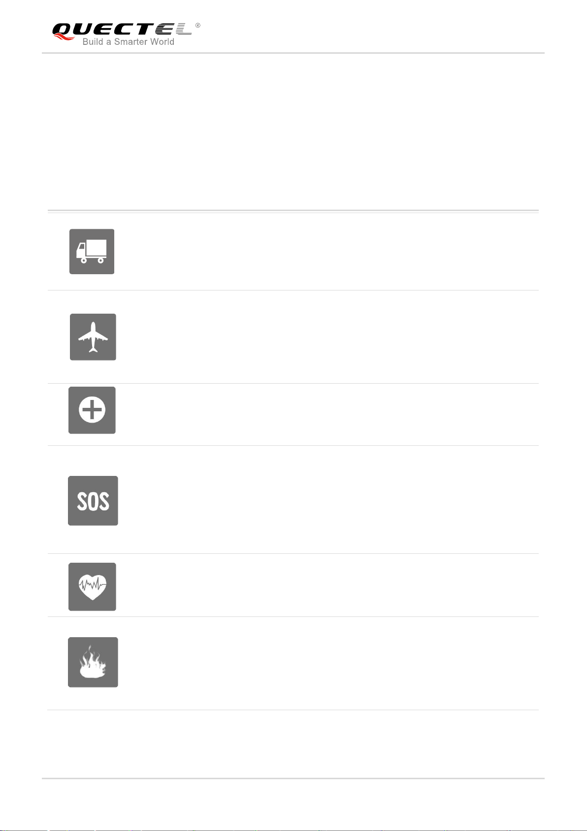
Full attention must be given to driving at all times in order to reduce the risk of an
accident. Using a mobile while driving (even with a handsfree kit) causes
distraction and can lead to an accident. Please comply with laws and regulations
restricting the use of wireless devices while driving.
Switch off the cellular terminal or mobile before boarding an aircraft. The operation
of wireless appliances in an aircraft is forbidden to prevent interference with
communication systems. If the device offers an Airplane Mode, then it should be
enabled prior to boarding an aircraft. Please consult the airline staff for more
restrictions on the use of wireless devices on boarding the aircraft.
Wireless devices may cause interference on sensitive medical equipment, so
please be aware of the restrictions on the use of wireless devices when in
hospitals, clinics or other healthcare facilities.
Cellular terminals or mobiles operating over radio signals and cellular network
cannot be guaranteed to connect in all possible conditions (for example, with
unpaid bills or with an invalid (U)SIM card). When emergent help is needed in such
conditions, please remember using emergency call. In order to make or receive a
call, the cellular terminal or mobile must be switched on in a service area with
adequate cellular signal strength.
The cellular terminal or mobile contains a transmitter and receiver. When it is ON, it
receives and transmits radio frequency signals. RF interference can occur if it is
used close to TV set, radio, computer or other electric equipment.
In locations with potentially explosive atmospheres, obey all posted signs to turn
off wireless devices such as your phone or other cellular terminals. Areas with
potentially explosive atmospheres include fuelling areas, below decks on boats,
fuel or chemical transfer or storage facilities, areas where the air contains
chemicals or particles such as grain, dust or metal powders, etc.
SC66 Hardware Design
1.1. Safety Information
The following safety precautions must be observed during all phases of operation, such as usage, service
or repair of any cellular terminal or mobile incorporating SC66 module. Manufacturers of the cellular
terminal should send the following safety information to users and operating personnel, and incorporate
these guidelines into all manuals supplied with the product. If not so, Quectel assumes no liability for
customers’ failure to comply with these precautions.
SC66_Hardware_Design 14 / 118
Smart LTE Module Series
Type
Frequency Bands
LTE-FDD
B1/B3/B5/B8
LTE-TDD
B34/B38/B39/B40/B41
WCDMA
B1/B8
TD-SCDMA
B34/B39
EVDO/CDMA
BC0
GSM
900/1800MHz
Wi-Fi 802.11a/b/g/n/ac
2402MHz~2482MHz; 5180MHz~5825MHz
SC66 Hardware Design
2 Product Concept
2.1. General Description
SC66 is a series of Smart LTE module based on Qualcomm platform and Android operating system, and
provides industrial grade performance. Its general features are listed below:
Support worldwide LTE-FDD, LTE-TDD, DC-HSDPA, DC-HSUPA, HSPA+, HSDPA, HSUPA,
WCDMA, TD-SCDMA, EVDO/CDMA, EDGE and GPRS coverage
Support short-range wireless communication via Wi-Fi 802.11a/b/g/n/ac and BT5.0 LE standards
Integrate GPS/GLONASS/BeiDou satellite positioning systems
Support multiple audio and video codecs
Built-in high performance AdrenoTM 512 graphics processing unit
Provide multiple audio and video input/output interfaces as well as abundant GPIO interfaces
SC66 are available in six variants: SC66-MW*, SC66-CE*, SC66-A*, SC66-J*, SC66-E*, SC66-W*.
The following table shows the supported frequency bands of SC66.
Table 1: SC66-CE* Frequency Bands
SC66_Hardware_Design 15 / 118
SC66 Hardware Design
BT5.0
2402MHz~2480MHz
GNSS
GPS: 1575.42MHz±1.023MHz
GLONASS: 1597.5MHz~1605.8MHz
BeiDou: 1561.098MHz±2.046MHz
Type
Frequency Bands
LTE-FDD
B2/B4/B5/B7/B12/B13/B14/B17/B25/B26/B66/B71
LTE-TDD
B41(200M)
WCDMA
B2/B4/B5
Wi-Fi 802.11a/b/g/n/ac
2402MHz~2482MHz; 5180MHz~5825MHz
BT 5.0
2402MHz~2480MHz
GNSS
GPS: 1575.42MHz±1.023MHz
GLONASS: 1597.5MHz~1605.8MHz
BeiDou: 1561.098MHz±2.046MHz
Type
Frequency Bands
LTE-FDD
B1/B3/B5/B8/B11/B18/B19/B21/B26/B28(A+B)
LTE-TDD
B41(120M)
WCDMA
B1/B6/B8/B19
Wi-Fi 802.11a/b/g/n/ac
2402MHz~2482MHz; 5180MHz~5825MHz
BT 5.0
2402MHz~2480MHz
GNSS
GPS: 1575.42MHz±1.023MHz
GLONASS: 1597.5MHz~1605.8MHz
BeiDou: 1561.098MHz±2.046MHz
Table 2: SC66-A* Frequency Bands
Smart LTE Module Series
Table 3: SC66-J* Frequency Bands
SC66_Hardware_Design 16 / 118
SC66 Hardware Design
Type
Frequency Bands
LTE-FDD
B1/B2/B3/B4/B5/B7/B8/B20/B28(A+B)
LTE-TDD
B38/B39/B40/B41(200M)
WCDMA
B1/B2/B4/B5/B8
GSM
B2/B3/B5/B8
Wi-Fi 802.11a/b/g/n/ac
2402MHz~2482MHz; 5180MHz~5825MHz
BT 5.0
2402MHz~2480MHz
GNSS
GPS: 1575.42MHz±1.023MHz
GLONASS: 1597.5MHz~1605.8MHz
BeiDou: 1561.098MHz±2.046MHz
Type
Frequency Bands
LTE-FDD
/
LTE-TDD
/
WCDMA
/
TD-SCDMA
/
CDMA
/
GSM
/
Wi-Fi 802.11a/b/g/n/ac
2402MHz~2482MHz; 5180MHz~5825MHz
BT 5.0
2402MHz~2480MHz
GNSS
/
Table 4: SC66-E* Frequency Bands
Smart LTE Module Series
Table 5: SC66-W* Frequency Bands
SC66_Hardware_Design 17 / 118
Smart LTE Module Series
“*” means under development. SC66-A、SC66-J、SC66-E、SC66-MW support WIFI_MIMO
Type
Frequency Bands
LTE-FDD
/
LTE-TDD
/
WCDMA
/
TD-SCDMA
/
CDMA
/
GSM
/
Wi-Fi 802.11a/b/g/n/ac
2402MHz~2482MHz; 5180MHz~5825MHz
BT 5.0
2402MHz~2480MHz
GNSS
/
NOTE
SC66 Hardware Design
Table 6: SC66-MW*(2*2 MIMO WIFI) Frequency Bands
SC66 is an SMD type module which can be embedded into applications through its 324 pins (including
152 LCC pads and 172 LGA pads). With a compact profile of 43.0mm × 44.0mm × 2.85mm, SC66 can
meet almost all requirements for M2M applications such as smart metering, smart home, security, routers,
wireless POS, mobile computing devices, PDA phone, tablet PC, etc.
SC66_Hardware_Design 18 / 118
Smart LTE Module Series
Features
Details
Application Processor
Customized 64-bit ARM v8-compliant applications processorCustomized
64-bit ARM v8-compliant applications processor
Kryo Gold: quad high-performance cores targeting 2.2 GHz
Kryo Silver: quad low-power cores targeting 1.843 GHz
two quad-core processors with 1MB L2 cache
Modem system
LTE Cat 6(FDD and TDD), 2*20 CA(40MHz)
GPU
Adreno 512 up to 650 MHzAdreno 512 up to 650 MHz
Memory
32GB eMMC + 3GB LPDDR4x(default)
64GB eMMC + 4GB LPDDR4x (optional)
Operating System
Android 9
Power Supply
VBAT Supply Voltage: 3.55V~4.4V
Typical 4.0V
Transmitting Power
Class 4 (33dBm±2dB) for EGSM900
Class 1 (30dBm±2dB) for DCS1800
Class E2 (27dBm±3dB) for EGSM900 8-PSK
Class E2 (26dBm±3dB) for DCS1800 8-PSK
Class 3 (24dBm+1/-3dB) for WCDMA bands
Class 3 (24dBm+3/-1dB) for EVDO/CDMA BC0
Class 2 (24dBm+1/-3dB) for TD-SCDMA bands
Class 3 (23dBm±2dB) for LTE-FDD bands
Class 3 (23dBm±2dB) for LTE-TDD bands
LTE Features
Support 3GPP R12 Cat 6* and Cat 4
Support 1.4 MHz to 20MHz RF bandwidth
Support Multiuser MIMO in DL direction
Cat 6* FDD: Max 300Mbps (DL)/Max 50Mbps (UL)
Cat 6* TDD: Max 265Mbps (DL)/Max 30Mbps (UL)
Cat 4 FDD: Max 150Mbps (DL)/Max 50Mbps (UL)
Cat 4 TDD: Max 130Mbps (DL)/Max 30Mbps (UL)
UMTS Features
Support 3GPP R9 DC-HSDPA/DC-HSUPA/HSPA+/HSDPA/HSUPA/WCDMA
Support QPSK, 16-QAM and 64-QAM modulation
DC-HSDPA: Max 42Mbps (DL)
DC-HSUPA: Max 11.2Mbps (UL)
SC66 Hardware Design
2.2. Key Features
The following table describes the detailed features of SC66 module.
Table 7: SC66 Key Features
SC66_Hardware_Design 19 / 118
Smart LTE Module Series
WCDMA: Max 384Kbps (DL)/Max 384Kbps (UL)
TD-SCDMA Features
Support CCSA Release 3 TD-SCDMA
Max 4.2Mbps (DL)/Max 2.2Mbps (UL)
CDMA2000 Features
Support 3GPP2 CDMA2000 1X Advanced, CDMA2000 1x EV-DO Rev.A
EVDO: Max 3.1Mbps (DL)/Max 1.8 Mbps (UL)
1X Advanced: Max 307.2Kbps (DL)/Max 307.2Kbps (UL)
GSM Features
R99
CSD: 9.6kbps, 14.4kbps
GPRS
Support GPRS multi-slot class 33 (33 by default)
Coding scheme: CS-1, CS-2, CS-3 and CS-4
Max 107Kbps (DL), 85.6Kbps (UL)
EDGE
Support EDGE multi-slot class 33 (33 by default)
Support GMSK and 8-PSK for different MCS (Modulation and Coding
Scheme)
Downlink coding schemes: CS 1-4 and MCS 1-9
Uplink coding schemes: CS 1-4 and MCS 1-9
Max 296Kbps (DL), 236.8Kbps (UL)
WLAN Features
2.4GHz/5GHz, support 802.11a/b/g/n/ac, maximally up to 433Mbps
Support AP and STA mode
Bluetooth Features
BT5.0 LE
GNSS Features
GPS/GLONASS/BeiDou
SMS
Text and PDU mode
Point-to-point MO and MT
SMS cell broadcast
LCM Interfaces
Support for MIPI_DSI and DP overTYPE-C for dual screen display
MIPI_DSI Supports up to 2560x1600@60fps
DP supports 4K@30fps
Camera Interfaces
Support three groups of 4-lane MIPI_CSI, up to 2.1Gbps per lane
Support 3 cameras (4-lane + 4-lane + 4-lane) or 4 cameras (4-lane + 4-lane +
2-lane + 1-lane)
up to 24MP with dual ISP
Video Codec
Video encoding and decoding: up to 4K @30fps
Concurrency: encoding up to 1080P @30fps; decoding up to 1080P @60fps
Audio Interfaces
Audio Input
Three analog microphone inputs, integrating internal bias voltage
Audio Output
Class AB stereo headphone output
Class AB earpiece differential output
Class D speaker differential amplifier output
SC66 Hardware Design
SC66_Hardware_Design 20 / 118
Smart LTE Module Series
1. 1) Within operation temperature range, the module is 3GPP compliant.
Audio Codec
EVRC, EVRC-B, EVRC-WB; G.711, G.729A/AB; GSM-FR, GSM-EFR,
GSM-HR; AMR-NB, AMR-WB, AMR-eAMR, AMR-BeAMR
USB Interface
Compliant with USB 3.1 and 2.0 specifications, with transmission rates up to
10Gbps on USB 3.1 and 480Mbps on USB 2.0.
Support USB OTG
Used for AT command communication, data transmission, software
debugging and firmware upgrade
UART Interfaces
4 UART Interfaces: DEBUG UART、UART6、UART1 and LPI_UART_2
UART6: 4-wire UART interface with RTS/CTS hardware flow control,
max rate up to 4Mbps
UART1: terface
DEBUG: 2-wire UART interface used for debugging
LPI_UART_2:low power uart, use is not recommended for the time being
SD Card Interface
Support SD 3.0
Support SD card hot-plug
(U)SIM Interfaces
2 (U)SIM interfaces
Support USIM/SIM card: 1.8V/2.95V
Support Dual SIM Dual Standby (supported by default)
I2C Interfaces
It supports up to five I2C interfaces, used for peripherals such as TP, camera,
sensor, etc.
I2S Interface
Supports two I2S, one of which is low power I2S
ADC Interfaces
2 general purpose ADC interfaces
SPI Interfaces
One SPI interfaces, only support master mode
Real Time Clock
Supported
Antenna Interfaces
Main antenna, Rx-diversity antenna, GNSS antenna and Wi-Fi/BT antenna
interfaces
Physical Characteristics
Size: (43.0±0.15)mm × (44.0±0.15)mm × (2.85±0.2)mm
Package: LCC + LGA
Weight: approx. 13.0g
Temperature Range
Operating temperature range: -35°C ~ +65°C
1)
Extended temperature range: -40°C ~ +75°C
2)
Storage temperature range: -40°C ~ +90°C
Firmware Upgrade
Over USB interface
RoHS
All hardware components are fully compliant with EU RoHS directive
NOTES
SC66 Hardware Design
SC66_Hardware_Design 21 / 118

Smart LTE Module Series
2. 2) Within extended temperature range, the module remains the ability to establish and maintain a
voice, SMS, data transmission, emergency call, etc. There is no unrecoverable malfunction. There
are also no effects on radio spectrum and no harm to radio network. Only one or more parameters like
P
out
might reduce in their value and exceed the specified tolerances. When the temperature returns to
the normal operating temperature levels, the module will meet 3GPP specifications again.
3. “*” means under development.
SC66 Hardware Design
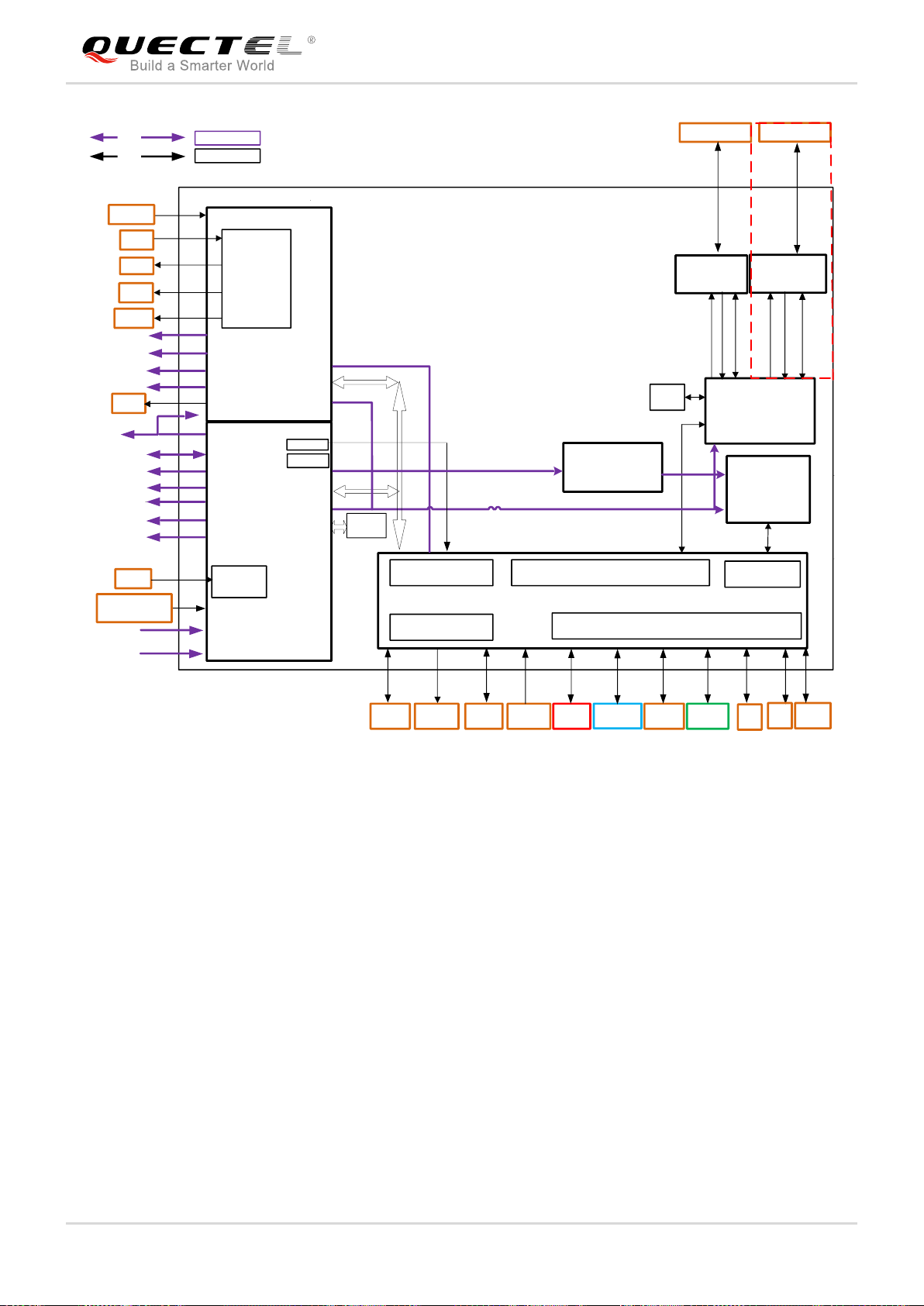
2.3. Functional Diagram
The following figure shows a block diagram of SC66 and illustrates the major functional parts.
Power management
Radio frequency
Baseband
LPDDR4X+eMMC flash
Peripheral interfaces
-- USB interface
-- (U)SIM interfaces
-- UART interfaces
-- SD card interface
-- I2C interfaces
- I2S interfaces
-- SPI interfaces
--ADC interfaces
-- LCM (MIPI) interfaces
-- TP (touch panel) interfaces
-- Camera (MIPI) interfaces
-- Audio interfaces
SC66_Hardware_Design 22 / 118
Smart LTE Module Series
Baseband
WCN
LPDDR
eMMC
FEM
XO
ANT_WIFI/BT
SD 3.0
UART
2×(U)SIM
USB
2.0&3.1
CAM
TPLCMSPI
EAR
SPK
MICs
RFCLK
BBCLK
MEM
Multimedia
Connectivity
Air Interface
Porcessors
Codec
Power
Signal
Power
Function
38.4MHZ
38.4
M
XO
Headset
VDD_RF
VOL_UP
VRTC
USIM1_VDD
USIM2_VDD
LDO13A_1P8
LDO11A_1P8
LDO14A_1P8
BATTERY
VPH_PWR
VBUS
GPIOs
13.2
769
I2C
I2S
PWRKEY
VOL DOWN
PM660L
SD_PU_VDD
SD_VDD
ADCs
LDO7B_3P125
LDO3B_2P8
HK ADC
&MPPs
PM660
PWM
PM-3003A
FEM
ANT_WIFI/BT
SC66 Hardware Design
This diagram just used for SC66-MW
SC66_Hardware_Design 23 / 118
Smart LTE Module Series
Baseband
Tranceiver
WCN
LPDDR
eMMC
FEM
XO
ANT_ GNSS
ANT_WIFI/BT
SD 3.0
UART
2×(U)SIM
USB
2.0&3.1
CAM
TPLCMSPI
EAR
SPK
MICs
RFCLK
BBCLK
MEM
Multimedia
Connectivity
Air Interface
Porcessors
Codec
Power
Signal
Power
Function
38.4MHZ
Duplexs
PA
Switch
SAW
LNA
SAW
SAW
Switch
SAW
ANT_DRX
ANT_ MAIN
38.4
M
XO
Headset
APT
VDD_RF
VOL_UP
C
1
VRTC
USIM1_VDD
USIM2_VDD
LDO13A_1P8
LDO11A_1P8
LDO14A_1P8
BATTERY
VPH_PWR
VBUS
GPIOs
13.2
769
I2C
I2S
PWRKEY
VOL DOWN
PM660L
SD_PU_VDD
SD_VDD
ADCs
LDO7B_3P125
LDO3B_2P8
HK ADC
&MPPs
PM660
PWM
PM-3003A
0欧姆跳贴
FEM
ANT_WIFI/BT
The red dotted frame is WIFI_MIMO path, which is not supported by SC66-CE and SC66-W.
NOTE
SC66 Hardware Design
-
2.4. Evaluation Board
Figure 1: Functional Diagram
In order to help customers develop applications with SC66 conveniently, Quectel supplies the evaluation
board, USB to RS232 converter cable, USB Type-C data cable, power adapter, earphone, antenna and
other peripherals to control or test the module.
SC66_Hardware_Design 24 / 118

Smart LTE Module Series
SC66 Hardware Design
3 Application Interfaces
3.1. General Description
SC66 is equipped with 324-pin 1.0mm pitch SMT pads that can be embedded into cellular application
platform. The following chapters provide the detailed description of pins/interfaces listed below.
Power supply
Turn on and off function
VRTC interface
Power Output
Charging interface
USB interface
UART interfaces
(U)SIM interfaces
SD card interface
GPIO interfaces
I2C interfaces
I2S interfaces
SPI interfaces
ADC interfaces
LCM interfaces
TP (touch panel) interfaces
Camera interfaces
Sensor interfaces
Audio interfaces
Emergency download interface
SC66_Hardware_Design 25 / 118
Smart LTE Module Series
313
314
315
316
317
318
319
306
307
308
309
310
311
312
299
300
301
302
303
304
305
292
293
294
295
296
297
298
285
286
287
288
289
290
291
278
279
280
281
282
283
284
271
272
273
274
275
276
277
264
265
266
268
269
270
267
257
258
259
261
262
263
260
1
2
3
4
5
6
7
8
9
10
11
12
13
14
15
16
17
18
19
20
21
22
23
39
41
42
43
44
45
46
47
48
49
51
52
53
54
40
50
55
56
57
585960
616263
64
323
321
322
2
4
25
26
27
29
28
30
31
32
33
34
35
36
37
38
656667
68
69
70
71
72
73
74
75
76
77
78
79
80
81
82
83
84
85
86
87
88
89
90
91
92
93
94
95
96
97
98
99
100
101
102
103
104
105
106
107
109
111
112
113
114
115
116
117
118
120
121
122
123
124
125
126
128
129
130
131
132
133
134
135
136
137
138
139
141
142
143
144
145
146
147
148
149
150
151
152
127
140
153
154
155
156
157
158
159
160
161
162
163
164
165
166
119
GND POWER AUDIO USB
(U)SIM SD TP LCM
CAMERA ANT UART GPIO
RESERVED
OTHERS
108
110
182
183
184
185
186
187
188
189
190
191
192
193
194
195
211
212
213
214
215
216
217
218
219
220
221
244
243
242
241
240
239
238
237
236
235
234
320
324
SC66 Hardware Design
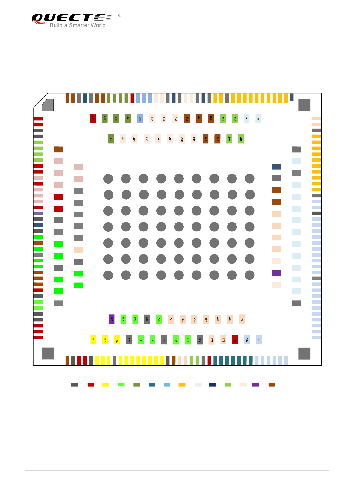
3.2. Pin Assignment
The following figure shows the pin assignment of SC66 module.
Figure 2: Pin Assignment (Top View)
SC66_Hardware_Design 26 / 118
SC66 Hardware Design
Type
Description
IO
Bidirectional
DI
Digital input
DO
Digital output
PI
Power input
PO
Power output
AI
Analog input
AO
Analog output
OD
Open drain
Power Supply
Pin Name
Pin No.
I/O
Description
DC Characteristics
Comment
VBAT
36,37, 38
PI/PO Power supply for the
module
Vmax=4.4V
Vmin=3.55V
Vnorm=4.0V
It must be able to
provide sufficient
current up to 3.0A.
It is suggested to
use a TVS to
increase voltage
surge withstand
capability.
VDD_RF
1, 2
PO
Connect to external
bypass capacitors to
eliminate voltage
fluctuation of RF
part.
Vmax=4.4V
Vmin=3.55V
Vnorm=4.0V
Do not load
externally.
VRTC
16
PI/P
Power supply for
VOmax=3.2V;
3.3. Pin Description
Table 8: I/O Parameters Definition
Smart LTE Module Series
The following tables show the SC66’s pin definition and electrical characteristics.
Table 9: Pin Description
SC66_Hardware_Design 27 / 118

Smart LTE Module Series
O
internal RTC circuit
When VBAT is not
connected
:
VI=2.1V~3.25V
LDO13A_1
P8
9
PO
1.8V output power
supply
Vnorm=1.8V
IOmax=20mA
Power supply for
external GPIO’s
pull up circuits and
level shift circuit.
LDO7B_3P
125
157
PO
3.125V output power
supply
Vnorm=3.125V
IOmax=150mA
Power supply only
for DP switch
LDO11A_1P
8
10
PO
1.8V output power
supply
Vnorm=1.8V
IOmax=150mA
Power supply for
I/O VDD of
cameras, LCDs
and TP etc.
LDO14A_1
P8
158
PO
1.8V output power
supply
Vnorm=1.8V
IOmax=150mA
Power supply for
Sensors. Add a
1.0uF~4.7uF
bypass capacitor if
used.
If unused, keep
this pin open.
LDO3B_2P
8
12
PO
2.8V output power
supply
Vnorm=2.8V
IOmax=600mA
Power supply for
sensor and LCM.
Add a 1.0uF~2.2uF
bypass capacitor if
used.
If unused, keep
this pin open.
VPH_PWR
30
PO
VBAT output power
supply
Vnorm=VBAT
IOmax=1000mA
Power supply for
other ICs.ICs
GND
3,4,18 ,
20,24,
31,34,
35,40,
Ground
SC66 Hardware Design
SC66_Hardware_Design 28 / 118
Smart LTE Module Series
43,47,
56,62,
87,98,
101,112,
125,128,
130,133,
135,148,
150,159,
160,163,
166,170,
173,176,
182,193,
195,219,
225,243,
257~323
Audio Interfaces
Pin Name
Pin No.
I/O
Description
DC Characteristics
Comment
MIC_BIAS
167
AO
Microphone bias
voltage
VO=1.6V~2.9V
MIC1_P
44
AI
Microphone positive
input for channel 1
MIC1_M
45
AI
Microphone
negative input for
channel 1
MIC_GND
168
Microphone
reference ground
If unused, it should
be connected to
GND
MIC2_P
46
AI
Microphone
Headset mic input
SC66 Hardware Design
SC66_Hardware_Design 29 / 118

Smart LTE Module Series
positive input for
headset
MIC3_P
169
AI
Microphone
positive input for
second mic
Second mic input
EAR_P
53
AO
Earpiece positive
output
EAR_M
52
AO
Earpiece negative
output
SPK_P
55
AO
Speaker positive
output
SPK_M
54
AO
Speaker negative
output
HPH_R
51
AO
Headphone right
channel output
HPH_REF
50
AI
Headphone
reference ground
It should be
connected to main
GND
HPH_L
49
AO
Headphone left
channel output
HS_DET
48
AI
Headset insertion
detection
Default high level
USB Interface
Pin Name
Pin No.
I/O
Description
DC Characteristics
Comment
USB_VBUS
41, 42
PI/P
O
Charging power
input.
Power supply
output for OTG
device.
USB/charger
insertion
detection.
Vmax=10V
Vmin=3.6V
Vnorm=5.0V
USB2_HS_
DM
25
IO
USB 2.0
differential data
bus (minus)
USB 2.0 standard
compliant
90Ω differential
impedance.
USB2_HS_
DP
26
IO
USB 2.0
differential data
bus (plus)
USB1_HS_
DM
33
IO
USB 2.0
differential data
bus (minus)
USB 2.0 standard
compliant
90Ω differential
impedance;
One part of the
SC66 Hardware Design
SC66_Hardware_Design 30 / 118

Smart LTE Module Series
USB1_HS_
DP
32
IO
USB 2.0
differential data
bus (plus)
TYPE-C.
USB_SS2_T
X_P
165
IO
USB 3.1
differential
transmit (plus)
USB 3.1 channel2
standard compliant
90Ω differential
impedance.
USB_SS2_T
X_M
164
IO
USB 3.1
differential
transmit (minus)
USB_SS2_
RX_P
162
IO
USB 3.1
differential receive
(plus)
USB_SS2_
RX_M
161
IO
USB 3.1
differential receive
(minus)
USB_SS1_
RX_P
171
IO
USB 3.1
differential receive
(plus)
USB 3.1 channel1
standard compliant
90Ω differential
impedance.
USB_SS1_
RX_M
172
IO
USB 3.1
differential receive
(minus)
USB_SS1_T
X _P
174
IO
USB 3.1
differential
transmit (plus)
90Ω differential
impedance.
USB_SS1_T
X _M
175
IO
USB 3.1
differential
transmit (minus)
USB_CC1
224
AI
USB Type-C
detection channel
1
When micro usb is
used ,it can be
used as ID pin
USB_CC2
223
AI
USB Type-C
detection channel
2
UUSB_TYP
EC
23
DI
TYPE-C&uUSB
configuration
control pin
When USB
TYPE-C is used, it
should be
connected to
VPH_PWR
through 10K
resistor. When
uUSB is used, it
should be
connected to GND
SC66 Hardware Design
SC66_Hardware_Design 31 / 118

Smart LTE Module Series
through 10K
resistor.
SS_DIR_IN
21
DI
CC status
detection pin
When USB
TYPE-C is used, it
should be
connected to
SS_DIR_OUT.
When uUSB is
used, it should be
connected to GND.
SS_DIR_OU
T
226
DO
CC status output
pin
When USB
TYPE-C is used, it
should be
connected to
SS_DIR_IN. When
uUSB is used, it
should be kept
open.
(U)SIM Interfaces
Pin Name
Pin
No.
I/O
Description
DC Characteristics
Comment
USIM1_DET
145
DI
(U)SIM1 card
hot-plug detection
VILmax=0.63V
VIHmin=1.17V
Active Low.
Require external
pull-up to 1.8V.
If unused, keep
this pin open.
USIM1_RST
144
DO
(U)SIM1 card
reset signal
VOLmax=0.4V
VOHmin=
0.8 × USIM1_VDD
USIM1_CLK
143
DO
(U)SIM1 card
clock signal
USIM1_DATA
142
IO
(U)SIM1 card data
signal
VILmax=
0.2 × USIM1_VDD
VIHmin=
0.7 × USIM1_VDD
VOLmax=0.4V
VOHmin=
0.8 × USIM1_VDD
USIM1_VDD
141
PO
(U)SIM1 card
power supply
Either 1.8V or
2.95V (U)SIM card
is supported.
USIM2_DET
256
DI
(U)SIM2 card
detection
VILmax=0.63V
VIHmin=1.17V
Active Low.
Need external
SC66 Hardware Design
SC66_Hardware_Design 32 / 118

Smart LTE Module Series
pull-up to 1.8V.
If unused, keep
this pin open.
USIM2_RST
207
DO
(U)SIM2 card
reset signal
VOLmax=0.4V
VOHmin=
0.8 × USIM2_VDD
USIM2_CLK
208
DO
(U)SIM2 card
clock signal
VOLmax=0.4V
VOHmin=
0.8 × USIM2_VDD
USIM2_DATA
209
IO
(U)SIM2 card data
signal
VILmax=
0.2 × USIM2_VDD
VIHmin=
0.7 × USIM2_VDD
VOLmax=0.4V
VOHmin=
0.8 × USIM2_VDD
USIM2_VDD
210
PO
(U)SIM2 card
power supply
Either 1.8V or
2.95V (U)SIM card
is supported.
UART Interfaces
Pin Name
Pin
I/O
Description
DC Characteristics
Comment
DEBUG_TXD
5
DO
DEBUG transmit
data.
Debug port by
default.
VOLmax=0.45V
VOHmin=1.35V
1.8V power
domain.
If unused, keep
these pins open.
DEBUG_RXD
6
DI
DEBUG receive
data.
Debug port by
default.
VILmax=0.63V
VIHmin=1.17V
UART1_TXD
7
DO
UART1 transmit
data
VOLmax=0.45V
VOHmin=1.35V
UART1_RXD
8
DI
UART1 receive
data
VILmax=0.63V
VIHmin=1.17V
UART6_RXD
198
DI
UART6 receive
data
VILmax=0.63V
VIHmin=1.17V
UART6_TXD
199
DO
UART6 transmit
data
VOLmax=0.45V
VOHmin=1.35V
UART6_RTS
245
DO
UART6 request to
send
VOLmax=0.45V
VOHmin=1.35V
UART6_CTS
246
DI
UART6 clear to
send
VILmax=0.63V
VIHmin=1.17V
SC66 Hardware Design
SC66_Hardware_Design 33 / 118

Smart LTE Module Series
LPI_UART_2_T
XD
60
DO
UART2 transmit
data
VOLmax=0.45V
VOHmin=1.35V
LPI_UART_2_R
XD
61
DI
UART2 receive
data
VILmax=0.63V
VIHmin=1.17V
SD Card Interface
Pin Name
Pin
I/O
Description
DC Characteristics
Comment
SD_CLK
70
DO
High speed digital
clock signal of SD
card
1.8V SD card:
VOLmax=0.45V
VOHmin=1.4V
2.95V SD card:
VOLmax=0.368V
VOHmin=2.125V
SD_CMD
69
IO
Command signal
of SD card
1.8V SD card:
VILmax=0.58V
VIHmin=1.27V
VOLmax=0.45V
VOHmin=1.4V
2.95V SD card:
VILmax=0.737V
VIHmin=1.843V
VOLmax=0.368V
VOHmin=2.125V
SD_DATA0
68
IO
High speed
bidirectional digital
signal lines of SD
card
SD_DATA1
67
IO
SD_DATA2
66
IO
SD_DATA3
65
IO
SD_DET
64
DI
SD card insertion
detection
VILmax=0.63V
VIHmin=1.17V
Active low.
SD_VDD
63
PO
Power supply for
SD card
Vnorm=2.95V
IOmax=600mA
SD_PU_VDD
179
PO
2.95V output
Vnorm=1.8V/2.95V
IOmax=50mA
Power supply for
SD card’s pull-up
circuit.
TP (Touch Panel) Interfaces
Pin Name
Pin N
I/O
Description
DC Characteristics
Comment
SC66 Hardware Design
SC66_Hardware_Design 34 / 118

Smart LTE Module Series
TP0_RST
138
DO
Reset signal of
touch panel (TP0)
VOLmax=0.45V
VOHmin=1.35V
1.8V power
domain. Active low.
TP0_INT
139
DI
Interrupt signal of
touch panel (TP0)
VILmax=0.63V
VIHmin=1.17V
1.8V power
domain.
TP0_I2C_SCL
140
OD
I2C clock signal of
touch panel (TP0)
1.8V power
domain.
TP0_I2C_SDA
206
OD
I2C data signal of
touch panel (TP0)
1.8V power
domain.
LCM Interfaces
Pin Name
Pin
No.
I/O
Description
DC Characteristics
Comment
PWM
152
DO
PWM Output
LCD0_RST
127
DO
LCD0 reset signal
VOLmax=0.45V
VOHmin=1.35V
1.8V power domain
It should not be
pulled up.
LCD0_TE
126
DI
LCD0 tearing
effect signal
VILmax=0.63V
VIHmin=1.17V
1.8V power
domain.
DSI0_CLK_N
116
AO
LCD0 MIPI clock
signal (negative)
85Ω differential
impedance.
DSI0_CLK_P
115
AO
LCD0 MIPI clock signal
(positive)
DSI0_LN0_N
118
AO
LCD0 MIPI lane 0 data
signal (negative)
85Ω differential
impedance.
DSI0_LN0_P
117
AO
LCD0 MIPI lane 0 data
signal (positive)
DSI0_LN1_N
120
AO
LCD0 MIPI lane 1 data
signal (negative)
85Ω differential
impedance.
DSI0_LN1_P
119
AO
LCD0 MIPI lane 1 data
signal (positive)
DSI0_LN2_N
122
AO
LCD0 MIPI lane 2 data
signal (negative)
85Ω differential
impedance.
DSI0_LN2_P
121
AO
LCD0 MIPI lane 2 data
signal (positive)
DSI0_LN3_N
124
AO
LCD0 MIPI lane 3 data
signal (negative)
85Ω differential
impedance.
DSI0_LN3_P
123
AO
LCD0 MIPI lane 3 data
signal (positive)
Camera Interfaces
SC66 Hardware Design
SC66_Hardware_Design 35 / 118

Smart LTE Module Series
Pin Name
Pin
No.
I/O
Description
DC
Characteristics
Comment
CSI1_CLK_N
89
AI
MIPI clock signal of rear
camera (negative)
85Ω differential
impedance.
CSI1_CLK_P
88
AI
MIPI clock signal of rear
camera (positive)
CSI1_LN0_N
91
AI
MIPI lane 0 data signal of
rear camera (negative)
85Ω differential
impedance.
CSI1_LN0_P
90
AI
MIPI lane 0 data signal of
rear camera (positive)
CSI1_LN1_N
93
AI
MIPI lane 1 data signal of
rear camera (negative)
85Ω differential
impedance.
CSI1_LN1_P
92
AI
MIPI lane 1 data signal of
rear camera (positive)
CSI1_LN2_N
95
AI
MIPI lane 2 data signal of
rear camera (negative)
85Ω differential
impedance.
CSI1_LN2_P
94
AI
MIPI lane 2 data signal of
rear camera (positive)
CSI1_LN3_N
97
AI
MIPI lane 3 data signal of
rear camera (negative)
85Ω differential
impedance.
CSI1_LN3_P
96
AI
MIPI lane 3 data signal of
rear camera (positive)
CSI2_CLK_N
184
AI
MIPI clock signal of depth
camera (negative)
85Ω differential
impedance.
CSI2_CLK_P
183
AI
MIPI clock signal of depth
camera (positive)
CSI2_LN0_N
186
AI
MIPI lane 0 data signal of
depth camera (negative)
85Ω differential
impedance.
CSI2_LN0_P
185
AI
MIPI lane 0 data signal of
depth camera (positive)
CSI2_LN1_N
188
AI
MIPI lane 1 data signal of
depth camera (negative)
85Ω differential
impedance.
CSI2_LN1_P
187
AI
MIPI lane 1 data signal of
depth camera (positive)
CSI2_LN2_N
190
AI
MIPI lane 2 data signal of
depth camera (negative)
85Ω differential
impedance.
CSI2_LN2_P
189
AI
MIPI lane 2 data signal of
depth camera (positive)
CSI2_LN3_N
192
AI
MIPI lane 3 data signal of
depth camera (negative)
85Ω differential
impedance.
CSI2_LN3_P
191
AI
MIPI lane 3 data signal of
depth camera (positive)
SC66 Hardware Design
SC66_Hardware_Design 36 / 118

Smart LTE Module Series
CSI0_CLK_N
78
AI
MIPI clock signal of front
camera (negative)
85Ω differential
impedance.
CSI0_CLK_P
77
AI
MIPI clock signal of front
camera (positive)
CSI0_LN0_N
80
AI
MIPI lane 0 data signal of
front camera (negative)
85Ω differential
impedance.
CSI0_LN0_P
79
AI
MIPI lane 0 data signal of
front camera (positive)
CSI0_LN1_N
82
AI
MIPI lane 1 data signal of
front camera (negative)
85Ω differential
impedance.
CSI0_LN1_P
81
AI
MIPI lane 1 data signal of
front camera (positive)
CSI0_LN2_N
84
AI
MIPI lane 2 data signal of
front camera (negative)
85Ω differential
impedance.
CSI0_LN2_P
83
AI
MIPI lane 2 data signal of
front camera (positive)
CSI0_LN3_N
86
AI
MIPI lane 3 data signal of
front camera (negative)
85Ω differential
impedance.
CSI0_LN3_P
85
AI
MIPI lane 3 data signal of
front camera (positive)
MCAM_MCLK
99
DO
Master clock signal of rear
camera
VOLmax=0.45V
VOHmin=1.35V
1.8V power
domain.
SCAM_MCLK
100
DO
Master clock signal of front
camera
1.8V power
domain.
MCAM_RST
74
DO
Reset signal of rear
camera
1.8V power
domain.
MCAM_PWDN
73
DO
Power down signal of rear
camera
1.8V power
domain.
SCAM_RST
72
DO
Reset signal of front
camera
1.8V power
domain.
SCAM_PWDN
71
DO
Power down signal of front
camera
1.8V power
domain.
CAM_I2C_SCL0
75
OD
I2C clock signal of camera
1.8V power
domain.
CAM_I2C_SDA
0
76
OD
I2C data signal of camera
1.8V power
domain.
DCAM_MCLK
194
DO
Master clock signal of
depth camera
VOLmax=0.45V
VOHmin=1.35V
1.8V power domain
SC66 Hardware Design
SC66_Hardware_Design 37 / 118

Smart LTE Module Series
DCAM_RST
180
DO
Reset signal of depth
camera
1.8V power domain
DCAM_PWDN
181
DO
Power down signal of
depth camera
1.8V power domain
CAM_I2C_SDA
1
197
OD
I2C data signal of depth
camera
1.8V power domain
CAM_I2C_SCL1
196
OD
I2C data signal of depth
camera
1.8V power
domain.
Keypad Interfaces
Pin Name
Pin
No.
I/O
Description
DC
Characteristics
Comment
PWRKEY
39
DI
Turn on/off the module
1.8V power domain
VOL_UP
146
DI
Volume up
The voltage follows
VBAT
VOL_DWN
147
DI
Volume down
1.8V power domain
SENSOR_I2C Interfaces
Pin Name
Pin
No.
I/O
Description
DC
Characteristics
Comment
SENSOR_I2C_
SCL
131
OD
I2C clock signal of
external sensors
1.8V power
domain.
SENSOR_I2C_
SDA
132
OD
I2C data signal of external
sensors
1.8V power
domain.
ADC Interfaces
Pin Name
Pin
No.
I/O
Description
DC
Characteristics
Comment
ADC0
151
AI
Max input
voltage:1.8V
ADC1
153
AI
Max input
voltage:1.8V
Antenna Interfaces
Pin Name
Pin
No.
I/O
Description
DC
Characteristics
Comment
ANT_MAIN
19
IO
Main antenna interface
50Ω impedance
SC66 Hardware Design
SC66_Hardware_Design 38 / 118

Smart LTE Module Series
ANT_DRX
149
AI
Diversity antenna interface
ANT_GNSS
134
AI
GNSS antenna interface
ANT_WIFI/BT
129
IO
Wi-Fi/BT antenna
interface
ANT_WIFI_MIM
O
324
IO
Wi-Fi_MIMO antenna
interface
SC66-CE、SC66-W
is not supported
GPIO Interfaces
Pin Name
Pin
No.
I/O
Description
DC
Characteristics
Comment
GPIO_20
113
IO
GPIO
VILmax=0.63V
VIHmin=1.17V
VOLmax=0.45V
VOLmin=1.35V
Can be used as
LCD1_RST
GPIO_21
231
IO
GPIO
GPIO_34
236
IO
GPIO
GPIO_40
238
IO
GPIO
GPIO_41
237
IO
GPIO
GPIO_42
137
IO
GPIO
Can be used as
TP1_INT
GPIO_43
136
IO
GPIO
Can be used as
TP1_RST
GPIO_55
178
IO
GPIO
GPIO_56
177
IO
GPIO
GPIO_72
239
IO
GPIO
GPIO_73
59
IO
GPIO
GPIO_74
58
IO
GPIO
GPIO_76
232
IO
GPIO
GPIO_77
240
IO
GPIO
ACCL_INT
252
IO
GPIO
GYRO_INT
255
IO
GPIO
MAG_INT
254
IO
GPIO
ALPS_INT
253
IO
GPIO
SC66 Hardware Design
SC66_Hardware_Design 39 / 118

Smart LTE Module Series
HALL_INT
218
IO
GPIO
GPIO_22
204
IO
GPIO
GPIO_23
205
IO
GPIO
GPIO_12
228
IO
GPIO
GPIO_13
227
IO
GPIO
GPIO_14
230
IO
GPIO
GPIO_15
229
IO
GPIO
GPIO_61
234
IO
GPIO
GPIO_03B
11
IO
GPIO
GPIO_08B
13
IO
GPIO
GPIO_04B
14
IO
GPIO
GPIO_05B
15
IO
GPIO
GPIO_11A
211
IO
GPIO
GPIO_13A
233
IO
GPIO
GRFC Interfaces
Pin Name
Pin No.
I/O
Description
DC
Characteristics
Comment
GRFC_19
242
IO
GPIO
Only for RF debug.
It should not be
pulled up.
GRFC_18
241
IO
GPIO
SPI Interfaces
Pin Name
Pin
No.
I/O
Description
DC
Characteristics
Comment
SPI_CS
201
DO
Chip selection signal
Only support
master mode
SPI_CLK
200
DO
Clock signal
SPI_MOSI
248
DO
Data output signal
SPI_MISO
247
DI
Data input signal
I2S Interfaces
SC66 Hardware Design
SC66_Hardware_Design 40 / 118

Smart LTE Module Series
Pin Name
Pin
No.
I/O
Description
DC
Characteristics
Comment
MI2S_2_WS
203
DO
I2S Word selection signal
MI2S_2_DATA0
249
IO
I2S DATA0 signal
MI2S_2_SCK
250
DO
I2S Serial clock signal
MI2S_2_DATA1
251
IO
I2S DATA1 signal
MI2S_2_MCLK
114
DO
I2S Main clock signal
LPI_MI2S_SCLK
212
DO
LPI_I2S serial clock signal
LPI_MI2S_WS
156
DO
LPI_I2S word selection
signal
LPI_MI2S_DATA
0
154
IO
LPI_I2S DATA0 signal
LPI_MI2S_DATA
1
155
IO
LPI_I2S DATA1 signal
Emergency Download Interface
Pin Name
Pin
No.
I/O
Description
DC
Characteristics
Comment
USB_BOOT
57
DI
Force the module to enter
into emergency download
mode
Pulled up to
LDO13A_1P8
during power-up
will force the
module to enter
into emergency
download mode.
Other Interfaces
Pin Name
Pin
No.
I/O
Description
DC
Characteristics
Comment
GNSS_PPS_OU
T
202
DO
LNA enable control
LNA enable control
CBL_PWR_N
22
DI
Used for configuring auto
power-on
If customers
require automatic
power-on, this pin
should be
shorted-to-ground
.
Reserved Interface
SC66 Hardware Design
SC66_Hardware_Design 41 / 118

SC66 Hardware Design
3.55V
Voltage
4.0V
Input current
3A
Pin Name
Pin
No.
I/O
Description
DC
Characteristics
Comment
RESERVED
17,21
3,
214,
215,
216,
217,
222,
235
Reserved pins
Keep these pins
open.
3.4. Power Supply
Smart LTE Module Series
3.4.1. Power Supply Pins
SC66 provides three VBAT pins、VDD_RF pins and one VPH_PWR pin. VBAT pins are dedicated for
connection with an external power supply. VDD_RF pins are designed for module’s RF part, and are used
to connect bypass capacitors so as to eliminate voltage fluctuation of RF part, VPH_PWR is used for
powering other devices.
3.4.2. Decrease Voltage Drop
The power supply range of the module is from 3.55V to 4.4V, and the recommended value is 4.0V. The
power supply performance, such as load capacity, voltage ripple, etc. directly influences the module’s
performance and stability. Under ultimate conditions, the module may have a transient peak current up to
3A. If the power supply capability is not sufficient, there will be voltage drops, and if the voltage drops
below 3.55V, the module will be powered off automatically. Therefore, please make sure the input voltage
will never drop below 3.55V.
SC66_Hardware_Design 42 / 118
Figure 3: Voltage Drop Sample

Smart LTE Module Series
Module
VDD_RF
VBAT
VBAT
C1
100uF
C6
100nF
C7
33pF
C8
10pF
+
C2
100nF
C3
33pF
C4
10pF
D1
SC66 Hardware Design
To decrease voltage drop, a bypass capacitor of about 100µF with low ESR (ESR=0.7Ω) should be used,
and a multi-layer ceramic chip capacitor (MLCC) array should also be reserved due to its ultra-low ESR. It
is recommended to use three ceramic capacitors (100nF, 33pF, 10pF) for composing the MLCC array,
and place these capacitors close to VBAT/VDD_RF pins. The width of VBAT trace should be no less than
3mm. In principle, the longer the VBAT trace is, the wider it will be.
In addition, in order to get a stable power source, it is suggested to use a 0.5W TVS and place it as close
to the VBAT pins as possible to increase voltage surge withstand capability. The following figure shows
the structure of the power supply.
Figure 4: Structure of Power Supply
3.4.3. Reference Design for Power Supply
The power design for the module is very important, as the performance of module largely depends on the
power source. The power supply of SC66 should be able to provide sufficient current up to 3A at least. By
default, it is recommended to use a battery to supply power for SC66. But if battery is not intended to be
used, it is recommended to use a regulator for SC66. If the voltage difference between the input and
output is not too high, it is suggested to use an LDO to supply power for the module. If there is a big
voltage difference between the input source and the desired output (VBAT), a buck converter is preferred
to be used as the power supply.
The following figure shows a reference design for +5V input power source which adopts an LDO
(MIC29502WU) from MICROCHIP. The typical output voltage is 4.0V and the maximum rated current is
5.0A.
SC66_Hardware_Design 43 / 118

Smart LTE Module Series
DC_IN
C1
C2
MIC29502WU U1
IN
OUT
EN
GND
ADJ
2 4
1
3
5
VBAT
100nF
C3
470uF
C4
100nF
R2
220K
100k
R3
470uF
470R
51K
R4
R1
1%
1%
1. It is recommended to switch off the power supply for module in abnormal state, and then switch on
the power to restart the module.
2. The module supports battery charging function by default. If the above power supply design is
adopted, please make sure the charging function is disabled by software, or connect VBAT to
Schottky diode in series to avoid the reverse current to the power supply chip.
3. When the battery power is reduced to 0%, the system will trigger automatic shutdown, so the design
of power supply should be consistent with the configuration of fuel gauge driver.
NOTES
SC66 Hardware Design
Figure 5: Reference Circuit of Power Supply
SC66_Hardware_Design 44 / 118

Smart LTE Module Series
Turn on pulse
PWRKEY
4.7K
47K
>1.6s
R1
R2
Q1
R3
1K
PWRKEY
S1
Close to S1
TVS
1K
SC66 Hardware Design
3.5. Turn on and off Scenarios
3.5.1. Turn on Module Using the PWRKEY
The module can be turned on by driving PWRKEY pin to a low level for at least 1.6s. PWRKEY pin is
pulled to 1.8V internally. It is recommended to use an open drain/collector driver to control the PWRKEY.
A simple reference circuit is illustrated in the following figure.
Figure 6: Turn on the Module Using Driving Circuit
Another way to control the PWRKEY is using a button directly. A TVS component is indispensable to be
placed nearby the button for ESD protection. A reference circuit is shown in the following figure.
Figure 7: Turn on the Module Using Keystroke
SC66_Hardware_Design 45 / 118

Smart LTE Module Series
CBL_PWR_N
(Pin22)
SC66
1K
Make sure that VBAT is stable before pulling down PWRKEY pin. The recommended time between them
is no less than 30ms. PWRKEY cannot be pulled down all the time.
VBAT
PWRKEY
Others
> 8
s
RESTART
NOTE
SC66 Hardware Design
In addition, when VBAT is powered on, the module will be powered on automatically. The reference
circuit is shown below:
Figure 8: Automatic Boot Reference Circuit
3.5.2. Restart the Module
Pull down PWRKEY for at least 1s, and then choose to turn off or restart the module when the prompt
window comes up.
Another way to Restart the module is to drive PWRKEY to a low level for at least 8s. The module will
execute Restart. The restart scenario is illustrated in the following figure.
Figure 9: Timing of Restarting Module
SC66_Hardware_Design 46 / 118

Smart LTE Module Series
VRTC
0R
100nF
1. 2.1V~3.25V input voltage range and 3.0V typical value for VRTC, when VBAT is disconnected.
2. When powered by VBAT, the RTC error is 100ppm. When powered by VRTC, the RTC error is about
200ppm.
3. If the rechargeable battery is used, the ESR of battery should be less than 2K, and it is recommended
to use the MS621FE FL11E of SEIKO.
NOTES
SC66 Hardware Design
3.6. VRTC Interface
The RTC (Real Time Clock) can be powered by an external power source through VRTC when the
module is powered down and there is no power supply for the VBAT. The external power source can be
rechargeable battery (such as button cells) according to application demands. The following reference
circuit design when an external battery is utilized for powering RTC.
Figure 10: RTC Powered by Rechargeable Button Cell
SC66_Hardware_Design 47 / 118

Smart LTE Module Series
Pin Name
Default Voltage (V)
Drive Current (mA)
Idle
LDO13A_1P8
1.8
20
Keep
LDO11A_1P8
1.8
150
/
LDO3B_2P8
2.8
600
/
LDO7B_3P125
3.125
150
/
LDO14A_1P8
1.8
150
Keep
SD_VDD
2.95
600
/
SD_PU_VDD
2.95
50 / USIM1_VDD
1.8/2.95
150
/
USIM2_VDD
1.8/2.95
150
/
VPH_PWR
Follow VBAT
1000
Keep
SC66 Hardware Design
3.7. Power Output
SC66 supports output of regulated voltages for peripheral circuits. During application, it is recommended
to use parallel capacitors (33pF and 10pF) in the circuit to suppress high frequency noise.
Table 10: Power Description
3.8. Battery Charge and Management
SC66 module supports a fully programmable switch-mode Li-ion battery charge function.It can charge
single-cell Li-ion and Li-polymer battery. Switching charging with Quick Charge 3.0 and 4.0 supports up to
3 A.The battery charger of SC66 module supports trickle charging, pre-charge, constant current charging
and constant voltage charging modes, which optimize the charging procedure for Li-ion batteries.
Trickle charging: When the battery voltage is below 2.1V, a 45mA trickle charging current is applied
to the battery.
Pre-charge: When the battery voltage is charged up and is between 2.4V and 3.0V (the maximum
pre-charge voltage is 2.4V~3.0V programmable, 3.0V by default), the system will enter into
pre-charge mode. The charging current is 500mA (100mA~1500mA programmable, 500mA by
default).
SC66_Hardware_Design 48 / 118

Smart LTE Module Series
Pin Name
Pin No.
I/O Description
Comment
USB_VBUS
41, 42
PI/PO
Charging power input.
Power supply output for OTG device.
USB/charger insertion detection.
Vmax=10V
Vmin=3.6V
Vnorm=5.0V
VBAT
36,37,
38
PI/PO
Power supply for the module
Vmax=4.4V
Vmin=3.55V
Vnorm=4.0V
BAT_PLUS
27
AI
Differential input signal of battery voltage
detection (plus)
Must be connected.
BAT_MINUS
28
AI
Differential input signal of battery voltage
detection (minus)
Must be connected.
BAT_THERM
29
AI
Battery temperature detection
Internally pulled up.
Externally connected
to GND via a 47K
NTC resistor.
SC66 Hardware Design
Constant current mode (CC mode): When the battery voltage is increased to between the
maximum pre-charge voltage and 4.35V (3.6V~4.5V programmable, 4.35V by default), the system
will switch to CC mode. The charging current is programmable from 0mA~3000mA. The default
charging current is 500mA for USB charging and 2A for adapter.
Constant voltage mode (CV mode): When the battery voltage reaches the final value 4.35V, the
system will switch to CV mode and the charging current will decrease gradually. When the charging
current reduces to about 100mA, the charging is completed.
Table 11: Pin Definition of Charging Interface
SC66 module supports battery temperature detection in the condition that the battery integrates a
thermistor (47K 1% NTC thermistor with B-constant of 4050K by default; SDNT1608X473F4050FTF of
SUNLORD is recommended) and the thermistor is connected to VBAT_THERM pin. If VBAT_THERM pin
is not connected, there will be malfunctions such as boot error, battery charging failure, battery level
display error, etc.
A reference design for battery charging circuit is shown as below.
SC66_Hardware_Design 49 / 118

Smart LTE Module Series
GND
BAT_THERM
VBAT
100uF
NTC
VBAT
33pF
1uF
ESD
USB_VBUS
Adapter or
USB
Module
Battery
C1 C2 C3
D1
D2
BAT_PLUS
ESD
BAT_MINUS
GND
SC66 Hardware Design
Figure 11: Reference Design for Battery Charging Circuit
SC66 offers a fuel gauge algorithm that is able to accurately estimate the battery’s state by current and
voltage monitor techniques. Using precise measurements of battery voltage, current, and temperature,
the fuel gauge provides a dependable state of charge estimate throughout the entire life of the battery and
across a broad range of operating conditions. It effectively protects the battery from over-discharging, and
also allows users to estimate the battery life based on the battery level so as to timely save important data
before completely power-down.
Mobile devices such as mobile phones and handheld POS systems are powered by batteries. When
different batteries are utilized, the charging and discharging curve has to be modified correspondingly so
as to achieve the best effect.
If thermistor is not available in the battery, or adapter is utilized for powering the module, then there is only
a need for VBAT and GND connection. In this case, the system may be unable to detect the battery,
which will cause power-on failure. In order to avoid this, VBAT_THERM should be connected to GND with
a 47KΩ resistor. BAT_PLUS and BAT_MINUS must be connected, otherwise there may be abnormalities
in use of the module. Among them, BAT_PLUS and BAT_MINUS are used for battery level detection, and
they should be routed as differential pair to ensure accuracy.
USB_VBUS can be powered by external power or USB adapter, mainly used for USB detection and
battery charging. The input of USB_VBUS is 3.6v ~10V, and the typical working voltage is 5V. The SC66
module supports the charge management of lithium ion batteries, but different types or capacities of
batteries require different charging parameters, and the maximum charging current can reach 3A.
SC66_Hardware_Design 50 / 118

Smart LTE Module Series
Pin Name
Pin No.
I/O
Description
Comment
USB_VBUS
41,42
PI/PO
Charging power input.
Power supply output for OTG
device.
USB/Charger insertion detection.
Vnorm=5.0V
USB1_HS_DM
33
IO
USB 2.0 differential data
Requires 90R
differential routing
USB1_HS_DP
32
IO
USB_SS1_RX_P
171
AI
USB 3.1 channel1 differential data
USB_SS1_RX_M
172
AI
USB_SS1_TX_P
174
AO
USB_SS1_TX_M
175
AO
USB_SS2_RX_M
161
AI
USB 3.1 channel2 differential data
SC66 Hardware Design
3.9. USB Interface
SC66 provides two USB interfaces,The interface is compatible with the USB 3.1/2.0 specification, and
can be used for USB OTG,TYPE-C,DP function. USB 3.1 has a maximum speed of 10Gbps, USB 2.0
supports up to 480Mbps with full speed (12Mbps) down compatibility. USB interface can be used for AT
command transmission, data transmission, software debugging and software upgrading.
SC66 also supports USB on-go(OTG) function. CC1 pin is used to detect whether the OTG device is
connected or not. CC1 is opened by default and high level is maintained. If a slave device is inserted,
CC1 will be pulled down and SC66 will be configured as host mode.
3.9.1. TYPE-C Interfaces
The TYPE-C interface has one set of usb2.0-compatible HS interfaces (USB1_HS_DP/M), and two
sets of SS interfaces that support USB3.1 (USB_SS1_RXP/M,USB_SS1_TXP/M&
USB_SS2_RXP/M,USB_SS2_TXP/M).
When TYPE-C is forward inserted, USB_CC1 detects the external device, and the data is transmitted
through USB_SS1;Conversely, when TYPE-C is inverted, USB_CC2 detects the external device, and the
data is transmitted through USB_SS2.
The following table shows the pin definition of USB interface.
Table 12: Pin Definition of USB Interface
SC66_Hardware_Design 51 / 118

Smart LTE Module Series
USB_SS2_RX_P
162
AI
USB_SS2_TX_M
164
AO
USB_SS2_TX_P
165
AO
UUSB_TYPEC
23
AI
uUSB&USB TYPE-C configure
slection pin
When USB TYPE-C is
used, it should be
connected to
VPH_PWR through
10K resistor. When
uUSB is used, it
should be connected
to GND through 10K
resistor.
USB_CC2
223
AI
USB TYPE-C Configure2
USB_CC1
224
AI
USB TYPE-C Configure1
When Micro usb is
used, it should be
used as ID pin
SS_DIR_IN
21
DI
CC status detection pin
When USB TYPE-C is
used, it should be
connected to
SS_DIR_OUT.When
uUSB is used,it
should be connected
to GND.
SS_DIR_OUT
226
DO
CC status output pin
When USB TYPE-C is
used, it should be
connected to
SS_DIR_IN.When
uUSB is used,it
should be huang up.
SC66 Hardware Design
SC66_Hardware_Design 52 / 118

Smart LTE Module Series
USB1_HS_DM
Module
USB
_
SS1
_RX_P
RX2+
RX2-
VBUS
CC1
D-
D+
TX2-
TX2+
CC2
USB_CC1
USB_CC2
RX1+
RX1TX1+
TX1-
USB Type-C
C6
C7
C8
C9
C10
C11
C12
C13
USB1_HS_DP
USB_VBUS
USB
_
SS1
_RX_M
USB
_
SS1
_TX_P
USB
_
SS1
_TX_M
USB
_
SS2
_RX_P
USB
_
SS2
_RX_M
USB
_
SS2
_TX_P
USB
_
_TX_M
SS2
B11
B10
A3
A2
B2
B3
A11
A10
UUSB_TYPEC
VPH_PWR
10K
SS_DIR_OUT
SS_DIR_IN
0R
SC66 Hardware Design
The following is a reference design for TYPE-C interface:
Figure 12: USB Type-C Interface Reference Design
In order to ensure USB performance, please follow the following principles while designing USB interface.
It is important to route the USB signal traces as differential pairs with total grounding. The impedance
of USB differential trace is 90Ω.
The ground reference plane must be continuous,without any cuts or any holes under the USB
signals,to ensure impedance continuity.
Pay attention to the influence of junction capacitance of ESD protection devices on USB data lines.
Typically, the capacitance value should be less than 2pF for USB 2.0 and less than 0.5pF for USB 3.1.
besides.Keep the ESD protection devices as close as possible to the USB connector.
Do not route signal traces under crystals, oscillators, magnetic devices ,audio signal,and RF signal
traces. It is important to route the USB differential traces in inner-layer with ground shielding on not
only upper and lower layers but also right and left sides.
Keep USB3.1 signal routing away from RF signal. Crossing and parallel with RF signal line is
forbidden. The isolation between USB3.0 signal and RF signal should be more than 90 db. Otherwise,
it will interfere with RF signal strongly.
Make sure the trace length difference between USB 3.1 RX/TX differential pairs do not exceed
Make sure the trace length difference between USB 2.0 DP/DM differential pairs do not exceed 2mm.
SC66_Hardware_Design 53 / 118
0.7mm.

Smart LTE Module Series
Pin No.
Signal
Length (mm)
Length Difference (DP-DM)
33
USB1_HS_DM
50.88
-0.32
32
USB1_HS_DP
51.20
171
USB_SS1_RX_P
39.96
0.00
172
USB_SS1_RX_M
39.96
174
USB_SS1_TX_P
39.69
-0.01
175
USB_SS1_TX_M
39.70
162
USB_SS2_RX_P
39.40
-0.18
161
USB_SS2_RX_M
39.57
165
USB_SS2_TX_P
39.85
-0.05
164
USB_SS2_TX_M
39.90
25
USB2_HS_DM
37.80
-0.26
26
USB2_HS_DP
37.54
220
DP_AUX_N
42.88
-0.94
221
DP_AUX_P
41.94
SC66 Hardware Design
For USB3.1,the Rx-to-Tx spacing should be three times the line width, Rx-and-Tx to other signals
spacing should be four times the line width;For USB2.0, the DP-to-DM spacing shouled be three
times the line width, DP-and-DM to other signals spacing should be four times line width.
For DisplayPort, The routing length difference between DP_AUX_N and DP_AUX_P should be less
than 7mm.
Table 13: USB Trace Length Inside the Module
3.9.2. DP Interfaces
SC66 also supports DisplayPort mode with 4 lanes up to 4K@30ps. It should be noticed that Display
mode cannot be supported with USB1 together, but it can be used with USB2 together.
The differences between USB mode and DisplayPort Mode are listed below:
SC66_Hardware_Design 54 / 118

Smart LTE Module Series
USB1_HS_DP
Module
USB
_
SS1
_RX_P
RX1+
RX1-
VBUS_ VBUS
CC1
D+
D-
TX1-
TX1+
CC2
USB_CC1
USB_CC2
RX2+
RX
2
TX2+
TX2-
USB Type_C
C6
C7
C8
C9
C10
C11
C12
C13
USB1_HS_DM
USB_VBUS
USB
_
SS1
_RX_M
USB
_
SS1
_TX_P
USB
_
SS1
_TX_M
USB
_
SS2
_RX_P
USB
_
SS2
_RX_M
USB
_
SS2
_TX_P
USB
_
_TX_M
SS2
SBU1
SBU2
OE
HSD2+
HSD2-
HSD1+
HSD1-
VCC
S
D+
D-
GND
LDO13A_1P8
AUX_P
AUX_N
LDO7B_3P125
100K
100K
GPIO_76
LDO13A_1P8
0.1uF
0.1uF
Module
100R@100MHZ
1UF
GPIO_21
SBU1
SBU2
2.2K
SGM7227YMS10 G/TR
Module Pin Name
USB Mode
DisplayPort Mode
USB_SS2_RX_P/M
USB_SS2_RX_P/M
DP_LANE0_P/M
USB_SS2_TX_P/M
USB_SS2_TX_P/M
DP_LANE1_P/M
USB_SS1_RX_P/M
USB_SS1_RX_P/M
DP_LANE3_P/M
USB_SS1_TX_P/M
USB_SS1_TX_P/M
DP_LANE2_P/M
DP_AUX_P/N
SBU1/2
AUX_P/N
USB1_HS_DP/DM
USB1_HS_DP/DM
USB1_HS_DP/M
USB_CC1/CC2
USB_CC1/CC2
HOTPLUG_DET/Vconn
VBUS
VBUS
VBUS
GND
GND
GND
SC66 Hardware Design
Table 14: The Differences between USB Mode and DisplayPort Mode
The design of Display Port is shown as below:
SC66_Hardware_Design 55 / 118

Smart LTE Module Series
USB2_DP
USB2_DM
Module
DP
DM
VBUS
ID
GND
100nF
4.7uF
VBUS
AW3605DNR
SW
VIN
EN
VOUT
VOUT
NC
GPIO_15
`
1UH
VPH_PWR
22uF
22uF
220uF
VBUS
GND
Pin Name
Pin No.
Comment
USB2_HS_DM
25
USB Differential Signal (minus)
USB2_HS_DP
26
USB Differential Signal (positive)
SC66 Hardware Design
Figure 13: Display Port interfaces
3.9.3. Host
SC66 supports two groups of USB, and USB1 is part of TYPE-C compatibility, USB2 is a separate part
that supports only the Host mode.
Table 15: USB2 configuration
USB2 realizes the reference circuit of Host mode:
Figure 14: USB2 Host
3.10. UART Interfaces
The module provides the following four UART interfaces:
UART6: 4-wire UART interface, hardware flow control supported
DEBUG UART: 2-wire UART interface, used for debugging by default
UART1: 2-wire UART interface
LPI_ UART _2: low power UART interface
SC66_Hardware_Design 56 / 118

Smart LTE Module Series
Pin Name
Pin No.
I/O
Description
Comment
DEBUG_TXD
5
DO
UART for Debug
1.8 power domain
DEBUG_RXD
6
DI
1.8 power domain
UART1_TXD
7
DO
UART1
1.8 power domain
UART1_RXD
8
DI
1.8 power domain
UART6_RXD
198
DI
UART6 Receive data
1.8 power domain
UART6_TXD
199
DO
UART6 Send data
1.8 power domain
UART6_CTS
246
DI
UART6 Clear sending
1.8 power domain
UART6_RTS
245
DO
UART6 Request sending
1.8 power domain
LPI_UART_2_
TXD
60
DO
UART2 Send data
1.8 power domain
LPI_UART_2_
RXD
61
DI
UART2 Receive data
1.8 power domain
SC66 Hardware Design
The following table shows the pin definition of UART interfaces.
Table 16: Pin Definition of UART Interfaces
UART6 is a 4-wire UART interface with 1.8V power domain. A level translator chip should be used if
customers’ application is equipped with a 3.3V UART interface. A level translator chip TXS0104EPWR
provided by Texas Instruments is recommended.
The following figure shows a reference design.
SC66_Hardware_Design 57 / 118

Smart LTE Module Series
VCCA
VCCB
OE
A1
A2
A3
A4
GND
B1
B2
B3
B4
LDO11A_1P8
UART
6_ RTS
UART6_ RXD
UART
6_ CTS
UART6_ TXD
RXD_3.3V
CTS_3.3V
TXD_3.3V
VDD_3.3V
TXS0104EPWR
C1
100pF
C2
U1
100
pF
RTS_3.3V
TXS0104EPWR
RXD_3.3V
CTS_3.3V
VCCA
Module
GND
GND
1.8V
VCCB
3.3V
DIN1
ROUT3
ROUT2
ROUT1
DIN4
DIN3
DIN2
DIN5
FORCEON
3.3V
DOUT1
DOUT2
DOUT3
DOUT4
DOUT5
RIN3
RIN2
RIN1
VCC GND
OE
SN65C3238 DB-9
RTS
TXD
CTS
RXD
GND
RTS_3.3V
UART6_TXD
UART6_RTS
UART6_RXD
UART6_CTS
TXD_1.8V
RTS_1.8V
RXD_1.8V
CTS_1.8V
/FORCEOFF
/INVALID
R1OUTB
TXD_3.3V
1.DEBUG UART, UART1,LPI_UART_2 are similar to UART6. Please refer to UART6 reference circuit
design for DEBUG UART, UART1,LPI_UART_2.
2.LPI_UART_2 is a low power UART and it is not recommended for the time being.
NOTE
SC66 Hardware Design
Figure 15: Reference Circuit with Level Translator Chip (for UART6)
The following figure is an example of connection between SC66 and PC. A voltage level translator and a
RS-232 level translator chip are recommended to be added between the module and PC, as shown
below:
Figure 16: RS232 Level Match Circuit (for UART5)
3.11. (U)SIM Interfaces
SC66_Hardware_Design 58 / 118

Smart LTE Module Series
Pin Name
Pin No.
I/O
Description
Comment
USIM1_DET
145
DI
(U)SIM1 card detection
Active Low.
Need external pull-up to 1.8V.
If unused, keep this pin open.
Disabled by default, and can be
enabled through software
configuration.
USIM1_RST
144
DO
(U)SIM1 card reset signal
USIM1_CLK
143
DO
(U)SIM1 card clock signal
USIM1_DATA
142
IO
(U)SIM1 card data signal
Pull up to USIM1 with a 10K
resistor.
USIM1_VDD
141
PO
(U)SIM1 card power supply
Either 1.8V or 2.95V (U)SIM card
is supported.
USIM2_DET
256
DI
(U)SIM2 card insertion
detection
Active low.
Need external pull-up to1.8V
If unused, keep this pin open.
USIM2_RST
207
DO
(U)SIM2 card reset signal
USIM2_CLK
208
DO
(U)SIM2 card clock signal
USIM2_DATA
209
IO
(U)SIM2 card data signal
Pull-up to USIM2 with a 10K
resistor.
USIM2_VDD
210
PO
(U)SIM2 card power supply
Either 1.8V or 2.95V (U)SIM card
is supported.
SC66 Hardware Design
SC66 provides two (U)SIM interfaces which both meet ETSI and IMT-2000 requirements. Dual SIM Dual
Standby is supported by default. Both 1.8V and 2.95V (U)SIM cards are supported, and the (U)SIM
interfaces are powered by the dedicated low dropout regulators from SC66 module.
Table 17: Pin Definition of (U)SIM Interfaces
SC66 supports (U)SIM card hot-plug via the USIM_DET pin, which is disabled by default and can be
enabled through software configuration. A reference circuit for (U)SIM interface with an 8-pin (U)SIM card
connector is shown as below.
SC66_Hardware_Design 59 / 118

Smart LTE Module Series
USIM_VDD
USIM_RST
USIM_CLK
USIM_DATA
USIM_DET
22R
100K
100nF
(U)SIM Card Connector
ESD
22pF
VCC
RST
CLK
IO
VPP
GND
USIM_VDD
10K
Module
R1
R2
C1
22pF22pF
C2 C3 C4
D1
22R
22R
R3
R4
R5
LDO13A_1P8
Module
USIM_ VDD
USIM_ RST
USIM_ CLK
USIM_ DATA
22R
22R
22R
100nF
ESD
22pF
VCC
RST
CLK IO
VPP
GND
10K
USIM_VDD
22pF
22pF
R1
C1
D1
R2
R3
R4
C2 C3 C4
USIM_ DET
(U)SIM Card Connector
SC66 Hardware Design
Figure 17: Reference Circuit for (U)SIM Interface with an 8-pin (U)SIM Card Connector
If there is no need to use USIM_DET, please keep it open. The following is a reference circuit for (U)SIM
interface with a 6-pin (U)SIM card connector.
Figure 18: Reference Circuit for (U)SIM Interface with a 6-pin (U)SIM Card Connector
In order to ensure good performance and avoid damage of (U)SIM cards, please follow the criteria below
in (U)SIM circuit design:
Keep placement of (U)SIM card connector as close to the module as possible. Keep the trace length
of (U)SIM card signals as less than 200mm as possible.
Keep (U)SIM card signals away from RF and VBAT traces.
A filter capacitor shall be reserved for USIM_VDD, and its maximum capacitance should not exceed
1uF. The capacitor should be placed near to (U)SIM card.
To avoid cross-talk between USIM_DATA and USIM_CLK, keep them away from each other and
shield them with ground. USIM_RST also needs ground protection.
SC66_Hardware_Design 60 / 118

Smart LTE Module Series
Pin Name
Pin No.
I/O Description
Comment
SD_VDD
63
PO
Power supply for SD card
Vnorm=2.95V
IOmax=600mA
SD_PU_VD
D
179
PO
SD card pull-up power
supply
Support 1.8V/2.95V power supply. The
maximum drive current is 50mA.
SD_CLK
70
DO
High speed digital clock
signal of SD card
Control characteristic impedance as
50Ω.
SD_CMD
69
I/O
Command signal of SD card
SD_DATA0
68
I/O
High speed bidirectional
digital signal lines of SD
card
SD_DATA1
67
I/O
SD_DATA2
66
I/O
SD_DATA3
65
I/O
SD_DET
64
DI
SD card insertion detection
Active low.
SC66 Hardware Design
In order to offer good ESD protection, it is recommended to add a TVS diode array with parasitic
capacitance not exceeding 50pF. The 22Ω resistors should be added in series between the module
and (U)SIM card so as to suppress EMI spurious transmission and enhance ESD protection. Please
note that the (U)SIM peripheral circuit should be close to the (U)SIM card connector.
The 22pF capacitors should be added in parallel on USIM_DATA, USIM_VDD, USIM_CLK and
USIM_RST signal lines so as to filter RF interference, and they should be placed as close to the
(U)SIM card connector as possible.
3.12. SD Card Interface
SC66 module supports SD 3.0 specifications. The pin definition of the SD card interface is shown below.
Table 18: Pin Definition of SD Card Interface
A reference circuit for SD card interface is shown as below.
SC66_Hardware_Design 61 / 118

Smart LTE Module Series
SD_CMD
120K
NM_51K
SD_DATA3
SD_DATA2
SD_CLK
SD_DATA0
SD_DET
SD_DATA1
P1-DAT2
P2-CD/DAT3
P3-CMD
P4-VDD
P5-CLK
P8-DAT1
GND
P6-VSS
P7-DAT0
DETECTIVE
GND
GND
GND
1
2
3
4
5
6
7
8
9
10
11
12
13
33R
33R
33R
33R
33R
33R
1K
33pF
4.7uF
Module
R1 R2
R3 R4
R5
R6
NM_51K
NM_10K
NM_51K
NM_51K
R7
R8
R9
R10
R11
R12
R13
D1 D2
D3
D4 D5
D6
D7
D8
C1
C2
SD Card Connector
LDO13A_1P8
SD_VDD
SD_PU_VDD
Pin No.
Signal
Length (mm)
Comment
70
SD_CLK
24.58
69
SD_CMD
24.32
68
SD_DATA0
24.33
SC66 Hardware Design
Figure 19: Reference Circuit for SD Card Interface
SD_VDD is a peripheral driver power supply for SD card. The maximum drive current is 600mA. Because
of the high drive current, it is recommended that the trace width is 0.5mm or above. In order to ensure the
stability of drive power, a 4.7uF and a 33pF capacitor should be added in parallel near the SD card
connector.
CMD, CLK, DATA0, DATA1, DATA2 and DATA3 are all high speed signal lines. In PCB design, please
control the characteristic impedance of them as 50Ω, and do not cross them with other traces. It is
recommended to route the trace on the inner layer of PCB, and keep the same trace length for CLK, CMD,
DATA0, DATA1, DATA2 and DATA3. CLK additionally needs ground shielding.
Layout guidelines:
Control impedance as 50Ω±10%, and ground shielding is required.
The difference in trace lengths among the clock, data, and command signals should be less than 2
mm.
The Bus length should be less than 100mm.
The spacing to all other signals and lane-to-lane should be at least one and a half times the line
width.
Table 19: SD Card Signal Trace Length Inside the Module
SC66_Hardware_Design 62 / 118

Smart LTE Module Series
67
SD_DATA1
24.33
66
SD_DATA2
24.21
65
SD_DATA3
24.25
引脚名
引脚号
GPIO
复位状态
备注
GPIO_20
113
GPIO_20
B-PD:nppukp
1)
GPIO_21
231
GPIO_21
B-PD:nppukp
Wakeup
2)
GPIO_34
236
GPIO_34
B-PD:nppukp
GPIO_40
238
GPIO_40
B-PD:nppukp
Wakeup
GPIO_41
237
GPIO_41
B-PD:nppukp
Wakeup
GPIO_42
137
GPIO_42
B-PD:nppukp
Wakeup
GPIO_43
136
GPIO_43
B-PD:nppukp
Wakeup
GPIO_55
178
GPIO_55
B-PD:nppukp
Wakeup
GPIO_56
177
GPIO_56
B-PD:nppukp
Wakeup
GPIO_72
239
GPIO_72
B-PD:nppukp
Wakeup
GPIO_73
59
GPIO_73
B-PD:nppukp
Wakeup
GPIO_74
58
GPIO_74
B-PD:nppukp
Wakeup
GPIO_76
232
GPIO_76
B-PD:nppukp
Wakeup
GPIO_77
240
GPIO_77
B-PD:nppukp
Wakeup
ACCL_INT
252
GPIO_68
B-PD:nppukp
Wakeup
GYRO_INT
255
GPIO_69
B-PD:nppukp
Wakeup
SC66 Hardware Design
3.13. GPIO Interfaces
SC66 has abundant GPIO interfaces with power domain of 1.8V. The pin definition is listed below.
Table 20: Pin Definition of GPIO Interfaces
SC66_Hardware_Design 63 / 118

Smart LTE Module Series
1.
1)
B: Bidirectional digital with CMOS input; PD:nppukp = Contains an internal pull-down.
2.
2)
Wakeup: interrupt pins that can wake up the system.
3. More details about GPIO configuration, please refer to the GPIO_Configuration.
MAG_INT
254
GPIO_70
B-PD:nppukp
Wakeup
ALPS_INT
253
GPIO_71
B-PD:nppukp
Wakeup
HALL_INT
218
GPIO_75
B-PD:nppukp
Wakeup
GPIO_22
204
GPIO_22
B-PD:nppukp
Wakeup
GPIO_23
205
GPIO_23
B-PD:nppukp
GPIO_12
228
GPIO_12
B-PD:nppukp
GPIO_13
227
GPIO_13
B-PD:nppukp
Wakeup
GPIO_14
230
GPIO_14
B-PD:nppukp
GPIO_15
229
GPIO_15
B-PD:nppukp
GPIO_61
234
GPIO_61
B-PD:nppukp
GPIO_03B
11
GPIO_03B
B-PD:nppukp
GPIO_08B
13
GPIO_08B
B-PD:nppukp
GPIO_04B
14
GPIO_04B
B-PD:nppukp
GPIO_05B
15
GPIO_05B
B-PD:nppukp
GPIO_11A
211
GPIO_11A
B-PD:nppukp
GPIO_13A
233
GPIO_13A
B-PD:nppukp
SC66 Hardware Design
3.14. I2C Interfaces
SC66 can provide up to 5 groups of I2C Interfaces. As an open drain output, each I2C interface
should be pulled up to 1.8V voltage. The SENSOR_I2C interface supports only sensors of the aDSP
architecture. CAM_I2C bus is controlled by Linux Kernel code and supports connection to video output
related devices.
SC66_Hardware_Design 64 / 118

SC66 Hardware Design
Pin Name
Pin No
I/O Description
Comment
TP0_I2C_SCL
140
OD
TP I2C clock
Used for TP0
TP0_I2C_SDA
206
OD
TP I2C data
CAM_I2C_SCL0
75
OD
CAM I2C clock
Used for main
and front camera
CAM_I2C_SDA0
76
OD
CAM I2C data
CAM_I2C_SCL1
196
OD
CAM I2C clock
Used for depth
camera
CAM_I2C_SDA1
197
OD
CAM I2C data
SENSOR_I2C_SCL
131
OD
Sensor I2C clock
Used for sensor
SENSOR_I2C_SDA
132
OD
Sensor I2C data
GPIO_22
204
OD
TP I2C data
The default
configuration is
GPIO port, which
can be reused as
I2C for TP1
GPIO_23
205
OD
TP I2C clock
Pin Name
Pin
No
I/O Description
Comment
MI2S_2_WS
203
DO
I2S word selection signal
I2S word selection (L/R)
MI2S_2_DATA0
249
IO
I2S Data0 signal
I2S serial data0 channel
MI2S_2_SCK
250
DO
I2S serial signal
I2S serial clock
MI2S_2_DATA1
251
IO
I2S Data1 signal
I2S serial data1 channel
MI2S_2_MCLK
114
DO
I2S Main clock signal
I2S main clock
Table 21: Pin Definition of I2C Interfaces
Smart LTE Module Series
3.15. I2S Interface
SC66 provides two I2S interfaces. The reference voltage field of the interface is 1.8v, and one group is
low-power I2S.
Table 22: Pin Definition of I2S Interface
SC66_Hardware_Design 65 / 118

Smart LTE Module Series
LPI_MI2S_SCLK
212
DO
LPI_I2S serial clock signal
I2S serial clock
LPI_MI2S_WS
156
DO
LPI_I2S word selection
signal
I2S word selection (L/R)
LPI_MI2S_DATA0
154
IO
LPI_I2S Data0 signal
I2S serial data0 channel
LPI_MI2S_DATA1
155
IO
LPI_I2S Data1 signal
I2S serial data1 channel
Pin Name
Pin No.
I/O Description
Comment
SPI3_MOSI
248
DO
Master out slave in of SPI
interface
SPI3_MISO
247
DI
Master in salve out of SPI
interface
SPI3_CS_N
201
DO
Chip selection signal of SPI
interface
SPI3_CLK
200
DO
Clock signal of SPI
interface
Pin Name
Pin No.
I/O Description
Comment
ADC0
151
AI
Universal ADC
interface
The maximum input voltage is
1.7v
ADC1
153
AI
Universal ADC
interface
The maximum input voltage is
1.7v
SC66 Hardware Design
3.16. SPI Interfaces
SC66 provides SPI interfaces which only support master mode.
Table 23: Pin Definition of SPI Interfaces
3.17. ADC Interfaces
SC66 provides two analog-to-digital converter (ADC) interfaces, and the pin definition is shown below.
Table 24: Pin Definition of ADC Interfaces
SC66_Hardware_Design 66 / 118

Smart LTE Module Series
Pin Name
Pin No.
I/O
Description
Comment
LDO11A_1P8
10
PO
1.8V output power supply
for LCM logic circuit and
DSI
LDO3B_2P8
12
PO
2.8V output power supply
for LCM analog circuits
PWM
152
DO
PWM signal output
LCD0_RST
127
DO
LCD0 reset signal
LCD0_TE
126
DI
LCD0 tearing effect signal
DSI0_CLK_N
116
AO
LCD0 MIPI clock signal
(negative)
DSI0_CLK_P
115
AO
LCD0 MIPI clock signal
(positive)
DSI0_LN0_N
118
AO
LCD0 MIPI lane 0 data
signal (negative)
DSI0_LN0_P
117
AO
LCD0 MIPI lane 0 data
signal (positive)
DSI0_LN1_N
120
AO
LCD0 MIPI lane 1 data
signal (negative)
DSI0_LN1_P
119
AO
LCD0 MIPI lane 1 data
signal (positive)
SC66 Hardware Design
The resolution of the ADC is up to 15 bits.
3.18. LCM Interfaces
SC66 video output interface (LCM interface) is based on MIPI_DSI standard and supports 8 groups of
high-speed differential data transmission and WQXGA display (resolution: 2560*1600),Support double
screen display, default DSI+DP (type-c), optional DSI0+DSI1. Note that DSI1 does not support screens
with command mode.
Table 25: Pin Definition of LCM Interfaces
SC66_Hardware_Design 67 / 118

Smart LTE Module Series
DSI0_LN2_N
122
AO
LCD0 MIPI lane 2 data
signal (negative)
DSI0_LN2_P
121
AO
LCD0 MIPI lane 2 data
signal (positive)
DSI0_LN3_N
124
AO
LCD0 MIPI lane 3 data
signal (negative)
DSI0_LN3_P
123
AO
LCD0 MIPI lane 3 data
signal (positive)
DSI1_CLK_N
103
AO
LCD1 MIPI clock signal
(negative)
DSI1_CLK_P
102
AO
LCD1 MIPI clock signal
(positive)
DSI1_LN0_N
105
AO
LCD1 MIPI lane 0 data
signal (negative)
DSI1_LN0_P
104
AO
LCD1 MIPI lane 0 data
signal (positive)
DSI1_LN1_N
107
AO
LCD1 MIPI lane 1 data
signal (negative)
DSI1_LN1_P
106
AO
LCD1 MIPI lane 1 data
signal (positive)
DSI1_LN2_N
109
AO
LCD1 MIPI lane 2 data
signal (negative)
DSI1_LN2_P
108
AO
LCD1 MIPI lane 2 data
signal (positive)
DSI1_LN3_N
111
AO
LCD1 MIPI lane 3 data
signal (negative)
DSI1_LN3_P
110
AO
LCD1 MIPI lane 3 data
signal (positive)
GPIO_20
113
DO
LCD1 复位信号
默认为 GPIO 口
GPIO_40
238
DO
LCD1 PWM 输出
默认为 GPIO 口
SC66 Hardware Design
The following are the reference designs for LCM interfaces.
LCM can use external backlight drive circuit according to customer requirement. The reference design of
the external backlight drive circuit is shown in the figure below, in which pins PWM (PIN152&PIN238) can
be used for backlight brightness adjustment.
SC66_Hardware_Design 68 / 118

Smart LTE Module Series
LCM0 _LED+
Module
2.2uF
背光驱动
LCM0_LED-
VPH_PWR
C1
PWM_OUT
(PIN152)
LCM1 _LED+
Module
2.2uF
背光驱动
LCM1_LED-
VPH_PWR
C1
PWM_OUT
(PIN238)
SC66 Hardware Design
Figure 20: LCM0 external backlight drive reference circuit
Figure 21: Reference Circuit Design for LCM1 Interface
SC66_Hardware_Design 69 / 118

Smart LTE Module Series
DSI0_CLK_P
LEDA
NC
LEDK
LPTE
NC (SDA-TP)
VIO18
NC (VTP-TP)
DSI0_LN3_P
LCD0_TE
LCD0_RST
DSI0_LN3_N
DSI0_LN2_P
DSI0_CLK_N
DSI0_LN2_N
RESET
LCD_ID
NC (SCL-TP)
NC (RST-TP)
NC (EINT-TP)
GND
VCC28
GND
MIPI_TDP3
MIPI_TDN3
GND
MIPI_TDP2
MIPI_TDN2
GND
MIPI_TDP1
MIPI_TDN1
GND
LDO3B_2P8
LDO11A_1P8
LCM0 _LED+
LCM0 _LED-
1
2
3
4
5
6
7
8
9
10
12
13
14
15
16
17
18
19
20
21
22
23
24
25
26
27
MIPI_TDP0
MIPI_TDN0
GND
MIPI_TCP
MIPI_TCN
29
28
30
3
4
5
6
3
4
5
6
3
4
5
6
3
4
5
6
DSI0_LN1_N
DSI0_LN1_P
DSI0_LN0_N
DSI0_LN0_P
1
2
3
4
5
6
11
1
2
1
2
1
2
1
2
100nF4.7uF
1uF
Module
LCM
FL1
FL2
FL3
FL4
FL5
EMI filter
C3C2C1
NC
GND
GND
GND
GND
ADC0
31
32
33
34
SC66 Hardware Design
Figure 22: Reference Circuit Design for LCM0 Interface
SC66_Hardware_Design 70 / 118

Smart LTE Module Series
DSI1_CLK_P
LEDA
NC
LEDK
NC (SDA-TP)
VIO18
NC (VTP-TP)
DSI1_LN3_P
LCD1_RST
DSI1_LN3_N
DSI1_LN2_P
DSI1_CLK_N
DSI1_LN2_N
RESET
LCD_ID
NC (SCL-TP)
NC (RST-TP)
NC (EINT-TP)
GND
VCC28
GND
MIPI_TDP3
MIPI_TDN3
GND
MIPI_TDP2
MIPI_TDN2
GND
MIPI_TDP1
MIPI_TDN1
GND
LDO3B_2P8
LDO11A_1P8
LCM1 _LED+
LCM1 _LED-
1
2
3
4
5
6
7
8
9
10
12
13
14
15
16
17
18
19
20
21
22
23
24
25
26
27
MIPI_TDP0
MIPI_TDN0
GND
MIPI_TCP
MIPI_TCN
29
28
30
3
4
5
6
3
4
5
6
3
4
5
6
3
4
5
6
DSI1_LN1_N
DSI1_LN1_P
DSI1_LN0_N
DSI1_LN0_P
1
2
3
4
5
6
11
1
2
1
2
1
2
1
2
100nF4.7uF
1uF
Module
LCM
FL1
FL2
FL3
FL4
FL5
EMI filter
C3C2C1
NC
GND
GND
GND
GND
ADC1
31
32
33
34
NC
SC66 Hardware Design
Figure 23: Reference Circuit Design for LCM1 Interface
MIPI are high speed signal lines. It is recommended that common-mode filters should be added in series
near the LCM connector, so as to improve protection against electromagnetic radiation interference.
ICMEF112P900MFR using ICT is recommended.
When compatible design with other displays is required, please connect the LCD_ID pin of LCM to the
module’s ADC pin, and please note that the output voltage of LCD_ID cannot exceed the voltage range of
ADC pin.
3.19. Touch Panel Interfaces
SC66 provides two I2C interfaces for connection with Touch Panel (TP), and also provides the
SC66_Hardware_Design 71 / 118

Smart LTE Module Series
Pin Name
Pin No
I/O
Description
Comment
GPIO_03B
11
PO
TP VDD power supply enable pin
Use external LDO power
supply
LDO11A_1P8
10
PO
1.8V output power supply
Pull-up power supply of I2C
Vnorm=1.8V
IOmax=300mA
TP0_INT
139
DI
Interrupt signal of touch panel (TP0)
TP0_RST
138
DO
Reset signal of touch panel (TP0)
TP0_I2C_
SCL
140
OD
I2C clock signal of touch panel
(TP0)
TP0_I2C_
SDA
206
OD
I2C data signal of touch panel (TP0)
SC66 Hardware Design
corresponding power supply and interrupt pins. The pin definition of touch panel interfaces is illustrated
below.
Table 26: Pin Definition of Touch Panel Interfaces
A reference design for touch panel interfaces is shown below.
SC66_Hardware_Design 72 / 118

Smart LTE Module Series
Module
2.2uF
LDO_IC
VPH_PWR
C1
GPIO_03B
R1
100K
C2
CTP_VDD
TP0_RST
TP0_I2C_SCL
TP0_I2C_SDA
TP0_INT
1
2
3
4
5
6
2.2K
2.2K
4.7uF
100nF
Module
RESET 1.8V
SCL 1.8V
SDA 1.8V
INT 1.8V
GND
VDD 2.8V
TP
R2
R1
C1 C2
D1 D2
D3
D4
D5
CTP_VDD
LDO11A_1P8
SC66 Hardware Design
3.20. Camera Interfaces
Based on standard MIPI CSI input interface, SC66 module supports 3 cameras (4-lane + 4-lane + 4-lane)
or 4 cameras (4-lane + 4-lane + 2-lane + 1-lane), with maximum pixels up to 24MP for SC66. The video
and photo quality are determined by various factors such as camera sensor, camera lens quality, etc.
SC66_Hardware_Design 73 / 118
Figure 24: Reference Circuit Design for Touch Panel Interfaces

Smart LTE Module Series
Pin Name
Pin No.
I/O
Description
Comment
GPIO_08B
13
DO
后置摄像头 DVDD 供电
LDO 使能管脚
GPIO_05B
15
DO
前置摄像头 DVDD 供电
LDO 使能管脚
Vnorm=1.8V
IOmax=150mA
LDO11A_1P8
10
PO
输出 1.8V;
给摄像头的 DOVDD 供电
Vnorm=2.8V
IOmax=600mA
LDO3B_2P8
12
PO
输出 2.8V;
摄像头 AF_VDD 电路供电
GPIO_04B
14
DO
摄像头 AVDD 供电 LDO 使
能管脚
CSI0_CLK_N
78
AI
前摄 MIPI 时钟负
CSI0_CLK_P
77
AI
前摄 MIPI 时钟正
CSI0_LN0_N
80
AI
前摄 MIPI 数据 0 负
CSI0_LN0_P
79
AI
前摄 MIPI 数据 0 正
CSI0_LN1_N
82
AI
前摄 MIPI 数据 1 负
CSI0_LN1_P
81
AI
前摄 MIPI 数据 1 正
CSI0_LN2_N
84
AI
前摄 MIPI 数据 2 负
CSI0_LN2_P
83
AI
前摄 MIPI 数据 2 正
CSI0_LN3_N
86
AI
前摄 MIPI 数据 3 负
CSI0_LN3_P
85
AI
前摄 MIPI 数据 3 正
CSI1_CLK_N
89
AI
后摄 MIPI 时钟负
CSI1_CLK_P
88
AI
后摄 MIPI 时钟正
CSI1_LN0_N
91
AI
后摄 MIPI 数据 0 负
CSI1_LN0_P
90
AI
后摄 MIPI 数据 0 正
CSI1_LN1_N
93
AI
后摄 MIPI 数据 1 负
CSI1_LN1_P
92
AI
后摄 MIPI 数据 1 正
CSI1_LN2_N
95
AI
后摄 MIPI 数据 2 负
SC66 Hardware Design
Table 27: Pin Definition of Camera Interfaces
SC66_Hardware_Design 74 / 118

Smart LTE Module Series
CSI1_LN2_P
94
AI
后摄 MIPI 数据 2 正
CSI1_LN3_N
97
AI
后摄 MIPI 数据 3 负
CSI1_LN3_P
96
AI
后摄 MIPI 数据 3 正
CSI2_CLK_N
184
AI
景深 MIPI 时钟负
CSI2_CLK_P
183
AI
景深 MIPI 时钟正
CSI2_LN0_N
186
AI
景深 MIPI 数据 0 负
CSI2_LN0_P
185
AI
景深 MIPI 数据 0 正
CSI2_LN1_N
188
AI
景深 MIPI 数据 1 负
CSI2_LN1_P
187
AI
景深 MIPI 数据 1 正
CSI2_LN2_N
190
AI
景深 MIPI 数据 2 负
CSI2_LN2_P
189
AI
景深 MIPI 数据 2 正
CSI2_LN3_N
192
AI
景深 MIPI 数据 3 负
CSI2_LN3_P
191
AI
景深 MIPI 数据 3 正
MCAM_MCLK
99
DO
后置摄像头时钟信号
SCAM_MCLK
100
DO
前置摄像头时钟信号
DCAM_MCLK
194
DO
景深摄像头时钟信号
MCAM_RST
74
DO
后置摄像头复位信号
SCAM_RST
72
DO
前置摄像头复位信号
DCAM_RST
180
DO
景深摄像头复位信号
MCAM_PWDN
73
DO
后置摄像头关断信号
SCAM_PWDN
71
DO
前置摄像头关断信号
DCAM_PWDN
181
DO
景深摄像头关断信号
CAM_I2C_SCL0
75
OD
前后摄 I2C 时钟信号
CAM_I2C_SDA0
76
OD
前后摄 I2C 数据信号
CAM_I2C_SDA1
197
OD
景深摄像头 I2C 数据信号
SC66 Hardware Design
SC66_Hardware_Design 75 / 118

Smart LTE Module Series
DVDD_REAR
Module
2.2uF
LDO_IC
VPH_PWR
C1
GPIO_08B
R1
100K
C2
AVDD
Module
2.2uF
LDO_IC
VPH_PWR
C5
GPIO_04B
R3
100K
C6
DVDD_FRONT
Module
2.2uF
LDO_IC
VPH_PWR
C3
R2
100K
C4
GPIO_5B
CAM_I2C_SCL1
196
OD
景深摄像头 I2C 时钟信号
SC66 Hardware Design
The following is a reference circuit design for two-camera applications.
Figure 25: Reference Circuit Design for Two-Camera Applications
SC66_Hardware_Design 76 / 118

Smart LTE Module Series
Rear camera connector
MCAM_PWDN
MCAM_MCLK
CAM_I2C_SDA0
CAM_I2C_SCL0
SCAM_RST
SCAM_PWDN
SCAM_MCLK
CSI1_CLK_P
CSI1_CLK_N
CSI0_CLK_P
CSI0_CLK_N
2.2K
2.2K
Front camera connector
4.7uF
1uF
1uF
MCAM_RST
EMI
EMI
EMI
EMI
EMI
EMI
EMI
EMI
EMI
EMI
AVDD
DVDD
DOVDD
1uF
CSI1_LN0_P
CSI1_LN0_N
CSI1_LN1_P
CSI1_LN1_N
CSI1_LN2_P
CSI1_LN2_N
CSI1_LN3_P
CSI1_LN3_N
CSI0_LN0_P
CSI0_LN0_N
CSI0_LN1_P
CSI0_LN1_N
CSI0_LN2_P
CSI0_LN2_N
CSI0_LN3_P
CSI0_LN3_N
DVDD
1uF
4.7uF
4.7uF
AVDD
DOVDD
AVDD
LDO3B_2P8
DVDD_REAR
LDO11A_1P8
AFVDD
DVDD_FRONT
CSI1 is used for rear camera, CSI2 is used for depth camera, and CSI0 is used for front camera,and LN2
as DATA, LN3 as CLK.
NOTE
SC66 Hardware Design
Figure 26: Reference Circuit Design for Two-Camera Applications
SC66_Hardware_Design 77 / 118

Smart LTE Module Series
Rear camera connector
MCAM_PWDN
MCAM_MCLK
CAM_I2C_SDA0
CAM_I2C_SCL0_
CSI1_LN3_P
CSI1_LN3_N
CSI1_LN2_P
CSI1_LN2_N
CSI1_LN1_P
CSI1_LN1_N
CSI1_LN0_P
CSI1_LN0_N
SCAM_RST
SCAM
_PWDN
SCAM
_MCLK
CSI2_CLK_P
CSI2_CLK_N
CSI2_LN0_P
CSI2_LN0_N
CSI0_LN1_P
CSI0_LN1_N
CSI0_LN0_P
CSI0_LN0_N
CSI1_CLK_P
CSI1_CLK_N
CSI0_CLK_P
CSI0_CLK_N
AVDD
2.2K
2.2K
Front camera connector
1uF
4.7uF
4.7uF
1uF
1uF
4.7uF
MCAM_RST
DCAM_PWDN
DCAM_MCLK
DCAM_I2C_SDA1
DCAM_I2C_SCL1
DCAM_RST
Depth camera connector
LDO3B_1P8
EMI
EMI
EMI
EMI
EMI
EMI
EMI
EMI
DVDD_REAR
1uF
2.2K
2.2K
DVDD
EMI
EMI
4.7
1uF
uF
AVDD
DOVDD
LDO11A_1P8
DVDD_FRONT
SC66 Hardware Design
The following is a reference circuit design for three-camera applications.
SC66_Hardware_Design 78 / 118
Figure 27: Reference Circuit Design for Three-Camera Applications

Smart LTE Module Series
CSI2 data lines CSI1_LN2_P, CSI_LN2_N, CSI_LN3_P and CSI_LN3_N can be multiplexed into MIPI
signals for the fourth camera in four-camera application.
Pin
Signal
length
Length(P-N)
116
DSI0_CLK_N
27.37
-0.10
115
DSI0_CLK_P
27.27
118
DSI0_LN0_N
27.03
0.04
117
DSI0_LN0_P
27.07
120
DSI0_LN1_N
26.65
-0.05
119
DSI0_LN1_P
26.60
122
DSI0_LN2_N
26.54
-0.01
NOTE
SC66 Hardware Design
3.20.1. Design Considerations
Special attention should be paid to the pin definition of LCM/camera connectors. Assure the SC66
and the connectors are correctly connected.
MIPI are high speed signal lines, supporting maximum data rate up to 2.1Gbps. The differential
impedance should be controlled as 85Ω. Additionally, it is recommended to route the trace on the
inner layer of PCB, and do not cross it with other traces. For the same group of DSI or CSI signals, all
the MIPI traces should keep the same length.
CSI/DSI should reference the ground at all times,ground cuts and voids in the path of CSI/DSI signals
should be avoided or removed.
Route the camera CLK signal in the inner layer of the PCB between ground fills
Spacing of the Lanes according to the following rules:
a) intrapair p to n : 1*trace width
b) Lane to Lane : 1.5*trace width
c) to all other signals : 2.5*trace width
Route MIPI traces according to the following rules:
a) The CSI trace length should not exceed 170mm and the DSI trace length should not exceed
110mm;
b) Control the differential impedance as 85Ω±10%;
c) Control intra-lane length difference within 0.7mm;
d) Control inter-lane length difference within 1.4mm.
Table 28: MIPI Trace Length Inside the Module
SC66_Hardware_Design 79 / 118

Smart LTE Module Series
121
DSI0_LN2_P
26.53
124
DSI0_LN3_N
27.31
-0.01
123
DSI0_LN3_P
27.30
103
DSI1_CLK_N
23.20
0.34
102
DSI1_CLK_P
23.54
105
DSI1_LN0_N
27.89
0.14
104
DSI1_LN0_P
28.03
107
DSI1_LN1_N
30.21
-0.30
106
DSI1_LN1_P
29.91
109
DSI1_LN2_N
33.56
0.16
108
DSI1_LN2_P
33.40
111
DSI1_LN3_N
37.35
-0.02
110
DSI1_LN3_P
37.33
89
CSI1_CLK_N
16.00
0.02
88
CSI1_CLK_P
15.98
91
CSI1_LN0_N
14.94
0.02
90
CSI1_LN0_P
14.96
93
CSI1_LN1_N
12.23
-0.16
92
CSI1_LN1_P
12.07
95
CSI1_LN2_N
10.69
-0.06
94
CSI1_LN2_P
10.75
97
CSI1_LN3_N
9.42
-0.01
96
CSI1_LN3_P
9.43
184
CSI2_CLK_N
17.46
-0.21
183
CSI2_CLK_P
17.67
186
CSI2_LN0_N
15.33
0..02
SC66 Hardware Design
SC66_Hardware_Design 80 / 118

Smart LTE Module Series
185
CSI2_LN0_P
15.35
188
CSI2_LN1_N
7.29
-0.03
187
CSI2_LN1_P
7.26
190
CSI2_LN2_N
3.73
0.52
189
CSI2_LN2_P
4.25
192
CSI2_LN3_N
6.77
0.27
191
CSI2_LN3_P
7.04
78
CSI0_CLK_N
25.37
-0.03
77
CSI0_CLK_P
25.34
80
CSI0_LN0_N
23.33
-0.10
79
CSI0_LN0_P
23.23
82
CSI0_LN1_N
22.19
0.36
81
CSI0_LN1_P
22.55
84
CSI0_LN2_N
20.06
-0.02
83
CSI0_LN2_P
20.04
86
CSI0_LN3_N
18.33
-0.28
85
CSI0_LN3_P
18.05
Pin Name
Pin No.
I/O
Description
Comment
SENSOR_I2C_SCL
131
OD
I2C clock signal of external sensor
Dedicated
SC66 Hardware Design
3.21. Sensor Interfaces
SC66 module supports communication with sensors via I2C interface, and it supports various sensors
such as acceleration sensor, gyroscopic sensor, compass, optical sensor, temperature sensor.
Table 29: Pin Definition of Sensor Interfaces
SC66_Hardware_Design 81 / 118

Smart LTE Module Series
SENSOR_I2C_SDA
132
OD
I2C data signal of external sensor
used for
sensors.
It cannot be
used for touch
panel, NFC,
I2C keyboard.
ALPS_INT
253
DI
Interrupt signal of optical sensor
MAG_INT
254
DI
Interrupt signal of direction sensor
(compass)
ACCL_INT
252
DI
Interrupt signal of acceleration sensor
GYRO_INT
255
DI
Interrupt signal of gyroscopic sensor
HALL_INT
218
DI
Interrupt signal of Hall sensor
Pin Name
Pin No.
I/O
Description
Comment
MIC1_P
44
AI
Microphone positive input for Main Mic
MIC1_N
45
AI
Microphone negative input for Main Mic
MIC_GND
168
Microphone reference ground
If unused, connect this
pin to the ground.
MIC2_P
46
AI
Microphone positive input for headset
MIC3_P
169
AI
Microphone positive input for secondary
mic
MIC_BIAS
167
AO
Microphone bias voltage
EAR_P
53
AO
Earpiece positive output
EAR_N
52
AO
Earpiece negative output
SPK_P
55
AO
Speaker positive output
SC66 Hardware Design
3.22. Audio Interfaces
SC66 module provides three analog input channels and three analog output channels. The following table
shows the pin definition.
Table 30: Pin Definition of Audio Interfaces
SC66_Hardware_Design 82 / 118

Smart LTE Module Series
MIC1_P
ECM-MIC
R2
R1
Module
D1
MIC1_N
33pF
C1
0R
0R
R3
0R
33pF
SPK_N
54
AO
Speaker negative output
HPH_R
51
AO
Headphone right channel output
HPH_REF
50
AI
Headphone reference ground
HPH_L
49
AO
Headphone left channel output
HS_DET
48
AI
Headset insertion detection
High level by default.
SC66 Hardware Design
The module offers three audio input channels, including one differential input pair and two
single-ended channels. The three sets of MICs are integrated with internal bias voltage.
The output voltage range of MIC_BIAS is programmable between 1.6V and 2.9V, and the maximum
output current is 3mA.
The earpiece interface uses differential output.
The loudspeaker interface uses differential output as well. The output channel is available with a
Class-D amplifier whose maximum output power is 1.5W when load is 8Ω.
The headphone interface features stereo left and right channel output, and headphone insertion
detection function is supported.
3.22.1. Reference Circuit Design for Microphone Interfaces
Figure 28: Reference Circuit Design for Analog ECM-type Microphone
SC66_Hardware_Design 83 / 118

Smart LTE Module Series
MIC3_P
33pF
MEMS-MIC
R2
R1
C2
Module
MIC_ GND
0R
C1
MIC_ BIAS
1
2
3
4
F1
D1
OUT
GND
GND
VDD
100nF
C4
0R
33pF
EAR_P
EAR_N
R2
33pF
33pF
33pF
C2
C3
C1
R1
Module
D1
D2
0R
0R
SC66 Hardware Design
Figure 29: Reference Circuit Design for MEMS-type Microphone
3.22.2. Reference Circuit Design for Earpiece Interface
Figure 30: Reference Circuit Design for Earpiece IInterface
SC66_Hardware_Design 84 / 118

Smart LTE Module Series
20K
ESD
MIC_GND
MIC2_P
HPH_L
HS_DET
HPH_R
HPH_REF
33pF
Module
R1
0R
6
3
4
5
2
1
33pF 33pF
C3
C4 C5
F3
F2
F1
D1 D2 D3
D4
F4
R2
R3
0R
EARP
EA
RN
F2
SPK_P
SPK_N
33pF
33pF
C1
C2
F1
Module
D1 D2
SC66 Hardware Design
3.22.3. Reference Circuit Design for Headphone Interface
Figure 31: Reference Circuit Design for Headphone Interface
3.22.4. Reference Circuit Design for Loudspeaker Interface
Figure 32: Reference Circuit Design for Loudspeaker Interface
3.22.5. Audio Interfaces Design Considerations
It is recommended to use the electret microphone with dual built-in capacitors (e.g. 10pF and 33pF) for
filtering out RF interference, thus reducing TDD noise. The 33pF capacitor is applied for filtering out RF
interference when the module is transmitting at EGSM900. Without placing this capacitor, TDD noise
could be heard. The 10pF capacitor here is used for filtering out RF interference at DCS1800. Please note
that the resonant frequency point of a capacitor largely depends on the material and production technique.
Therefore, customers would have to discuss with their capacitor vendors to choose the most suitable
capacitor for filtering out high-frequency noises.
SC66_Hardware_Design 85 / 118

Smart LTE Module Series
LDO13A_1P8
S1
Module
USB_BOOT
R1
10K
SC66 Hardware Design
The severity degree of the RF interference in the voice channel during GSM transmitting largely depends
on the application design. In some cases, EGSM900 TDD noise is more severe; while in other cases,
DCS1800 TDD noise is more obvious. Therefore, a suitable capacitor can be selected based on the test
results. Sometimes, even no RF filtering capacitor is required.
In order to decrease radio or other signal interference, RF antennas should be placed away from audio
interfaces and audio traces. Power traces cannot be parallel with and also should be far away from the
audio traces.
The differential audio traces must be routed according to the differential signal layout rule.
3.23. Emergency Download Interface
USB_BOOT is an emergency download interface. Pull up to LDO13A_1P8 during power-up will force the
module enter into emergency download mode. This is an emergency option when there are failures such
as abnormal startup or operation. For convenient firmware upgrade and debugging in the future, please
reverse the reference circuit design shown as below.
Figure 33: Reference Circuit Design for Emergency Download Interface
SC66_Hardware_Design 86 / 118

Smart LTE Module Series
Standard
Rate
Output Power
2.4GHz
802.11b
1Mbps
16dBm±2.5dB
802.11b
11Mbps
16dBm±2.5dB
802.11g
6Mbps
16dBm±2.5dB
SC66 Hardware Design
4 Wi-Fi and BT
SC66 module provides two shared antenna interface ANT_WIFI/BT and ANT_WIFI_MIMO for Wi-Fi and
Bluetooth (BT) functions(SC66-CE and SC66-W just support ANT_WIFI/BT). The interface impedance is
50Ω. External antennas such as PCB antenna, sucker antenna and ceramic antenna can be connected to
the module via the interface, so as to achieve Wi-Fi and BT functions.
4.1. Wi-Fi Overview
SC66 module supports 2.4GHz and 5GHz dual-band WLAN wireless communication based on IEEE
802.11a/b/g/n/ac standard protocols. The maximum data rate is up to 433Mbps.
The features are as below:
Support Wake-on-WLAN (WoWLAN)
Support ad hoc mode
Support WAPI SMS4 hardware encryption
Support AP mode
Support Wi-Fi Direct
Support MCS 0-7 for HT20 and HT40
Support MCS 0-8 for VHT20
Support MCS 0-9 for VHT40 and VHT80
4.1.1. Wi-Fi Performance
The following table lists the Wi-Fi transmitting and receiving performance of SC66 module.
Table 31: Wi-Fi Transmitting Performance
SC66_Hardware_Design 87 / 118

Smart LTE Module Series
802.11g
54Mbps
14dBm±2.5dB
802.11n HT20
MCS0
15dBm±2.5dB
802.11n HT20
MCS7
13dBm±2.5dB
802.11n HT40
MCS0
14dBm±2.5dB
802.11n HT40
MCS7
13dBm±2.5dB
5GHz
802.11a
6Mbps
15dBm±2.5dB
802.11a
54Mbps
13dBm±2.5dB
802.11n HT20
MCS0
15dBm±2.5dB
802.11n HT20
MCS7
13dBm±2.5dB
802.11n HT40
MCS0
15dBm±2.5dB
802.11n HT40
MCS7
13dBm±2.5dB
802.11ac VHT20
MCS0
14dBm±2.5dB
802.11ac VHT20
MCS8
13dBm±2.5dB
802.11ac VHT40
MCS0
13dBm±2.5dB
802.11ac VHT40
MCS9
12dBm±2.5dB
802.11ac VHT80
MCS0
13dBm±2.5dB
802.11ac VHT80
MCS9
12dBm±2.5dB
Standard
Rate
Sensitivity
2.4GHz
802.11b
1Mbps
-96dBm
802.11b
11Mbps
-87dBm
802.11g
6Mbps
-91dBm
802.11g
54Mbps
-73dBm
802.11n HT20
MCS0
-90dBm
SC66 Hardware Design
Table 32: Wi-Fi Receiving Performance
SC66_Hardware_Design 88 / 118

Smart LTE Module Series
802.11n HT20
MCS7
-72dBm
802.11n HT40
MCS0
-87dBm
802.11n HT40
MCS7
-68dBm
5GHz
802.11a
6Mbps
-90dBm
802.11a
54Mbps
-70dBm
802.11n HT20
MCS0
-88dBm
802.11n HT20
MCS7
-69dBm
802.11n HT40
MCS0
-86dBm
802.11n HT40
MCS7
-66dBm
802.11ac VHT20
MCS8
-68dBm
802.11ac VHT40
MCS9
-64dBm
802.11ac VHT80
MCS9
-60dBm
SC66 Hardware Design
Reference specifications are listed below:
IEEE 802.11n WLAN MAC and PHY, October 2009 + IEEE 802.11-2007 WLAN MAC and PHY, June
2007
IEEE Std 802.11b, IEEE Std 802.11d, IEEE Std 802.11e, IEEE Std 802.11g, IEEE Std 802.11i: IEEE
802.11-2007 WLAN MAC and PHY, June 2007
4.2. BT Overview
SC66 module supports BT4.2 (BR/EDR+BLE) specifications, as well as GFSK, 8-DPSK, π/4-DQPSK
modulation modes.
Maximally support up to 7 wireless connections
Maximally support up to 3.5 piconets at the same time
Support one SCO or eSCO (Extended Synchronous Connection Oriented) connection
The BR/EDR channel bandwidth is 1MHz, and can accommodate 79 channels. The BLE channel
bandwidth is 2MHz, and can accommodate 40 channels.
SC66_Hardware_Design 89 / 118

Smart LTE Module Series
Version
Data rate
Maximum Application Throughput
Comment
1.2
1Mbit/s
> 80Kbit/s
2.0+EDR
3Mbit/s
> 80Kbit/s
3.0+HS
24Mbit/s
Reference to 3.0+HS
4.0
24Mbit/s
Reference to 4.0 LE
5.0
48Mbit/S
Reference to 5.0 LE
Transmitter Performance
Packet Types
DH5
2-DH5
3-DH5
Transmitting Power
10dBm±2.5dB
8dBm±2.5dB
8dBm±2.5dB
Receiver Performance
Packet Types
DH5
2-DH5
3-DH5
Receiving Sensitivity
-92dBm
-91dBm
-83dBm
SC66 Hardware Design
Table 33: BT Data Rate and Versions
Reference specifications are listed below:
Bluetooth Radio Frequency TSS and TP Specification 1.2/2.0/2.0 + EDR/2.1/2.1+ EDR/3.0/3.0 + HS,
August 6, 2009
Bluetooth Low Energy RF PHY Test Specification, RF-PHY.TS/4.0.0, December 15, 2009
Bluetooth 5.0 RF-PHY Cover Standard:RF-PHY.TS.5.0.0, December 06, 2016
4.2.1. BT Performance
The following table lists the BT transmitting and receiving performance of SC66 module.
Table 34: BT Transmitting and Receiving Performance
SC66_Hardware_Design 90 / 118

Smart LTE Module Series
Parameter
Description
Typ.
Unit
Sensitivity (GNSS)
Cold start
TBD
dBm
Reacquisition
TBD
dBm
Tracking
TBD
dBm
TTFF (GNSS)
Cold start
TBD
s
Warm start
TBD
s
Hot start
TBD
s
Static Drift (GNSS)
CEP-50
TBD
m
SC66 Hardware Design
5 GNSS
SC66 module integrates a Qualcomm IZat™ GNSS engine (Gen 9) which supports multiple positioning
and navigation systems including GPS, GLONASS and BeiDou. With an embedded LNA, the module
provides greatly improved positioning accuracy.
5.1. GNSS Performance
The following table lists the GNSS performance of SC66 module in conduction mode.
Table 35: GNSS Performance
SC66_Hardware_Design 91 / 118

Smart LTE Module Series
SC66 Hardware Design
5.2. GNSS RF Design Guidelines
Bad design of antenna and layout may cause reduced GNSS receiving sensitivity, longer GNSS
positioning time, or reduced positioning accuracy. In order to avoid these, please follow the design rules
listed below:
Maximize the distance between the GNSS RF part and the GPRS RF part (including trace routing
and antenna layout) to avoid mutual interference.
In user systems, GNSS RF signal lines and RF components should be placed far away from high
speed circuits, switched-mode power supplies, power inductors, the clock circuit of single-chip
microcomputers, etc.
For applications with harsh electromagnetic environment or high ESD-protection requirements, it is
recommended to add ESD protective diodes for the antenna interface. Only diodes with ultra-low
junction capacitance such as 0.5pF can be selected. Otherwise, there will be effects on the
impedance characteristic of RF circuit loop, or attenuation of bypass RF signal may be caused.
Control the impedance of either feeder line or PCB trace as 50Ω, and keep the trace length as short
as possible.
Refer to Chapter 6.3 for GNSS antenna reference circuit designs.
SC66_Hardware_Design 92 / 118

Smart LTE Module Series
Pin Name
Pin No.
I/O
Description
Comment
ANT_MAIN
19
IO
Main antenna interface
50Ω impedance
ANT_DRX
149
AI
Diversity and MIMO
antenna interface
50Ω impedance
3GPP Band
Receive
Transmit
Unit
EGSM900
925~960
880~915
MHz
DCS1800
1805~1880
1710~1785
MHz
WCDMA B1
2110~2170
1920~1980
MHz
WCDMA B8
925~960
880~915
MHz
EVDO/CDMA BC0
869~894
824~849
MHz
TD-SCDMA B34
2010~2025
2010~2025
MHz
TD-SCDMA B39
1880~1920
1880~1920
MHz
SC66 Hardware Design
6 Antenna Interfaces
SC66 provides five antenna interfaces for main antenna, Rx-diversity/MIMO antenna, GNSS antenna,
Wi-Fi/BT antenna and WIFI_MIMO antenna. respectively. The antenna ports have an impedance of 50Ω.
6.1. Main/Rx-diversity Antenna Interfaces
The pin definition of main/Rx-diversity antenna interfaces is shown below.
Table 36: Pin Definition of Main/Rx-diversity Antenna Interfaces
The operating frequencies of SC66 module are listed in the following table.
Table 37: SC66-CE* Module Operating Frequencies
SC66_Hardware_Design 93 / 118

Smart LTE Module Series
LTE-FDD B1
2110~2170
1920~1980
MHz
LTE-FDD B3
1805~1880
1710~1785
MHz
LTE-FDD B5
824~849
869~894
MHz
LTE-FDD B8
925~960
880~915
MHz
LTE-TDD B34
2010~2025
2010~2025
MHz
LTE-TDD B38
2570~2620
2570~2620
MHz
LTE-TDD B39
1880~1920
1880~1920
MHz
LTE-TDD B40
2300~2400
2300~2400
MHz
LTE-TDD B41 1)
2555~2655
2555~2655
MHz
频段
下行
上行
单位
WCDMA B2
1930~1990
1850~1910
MHz
WCDMA B4
2110~2155
1710~1755
MHz
WCDMA B5
871~892
826~847
MHz
LTE-FDD B2
1930~1990
1850~1910
MHz
LTE-FDD B4
2110~2155
1710~1755
MHz
LTE-FDD B5
869~894
824~849
MHz
LTE-FDD B7
2620~2690
2500~2570
MHz
LTE-FDD B12
729~746
699~716
MHz
LTE-FDD B13
746~756
777~787
MHz
LTE-FDD B14
758~768
788~798
MHz
LTE-FDD B17
734~746
704~716
MHz
LTE-FDD B25
1930~1995
1850~1915
MHz
LTE-FDD B26
859~894
814~849
MHz
SC66 Hardware Design
Table 38: SC66-A* Module Operating Frequencies
SC66_Hardware_Design 94 / 118

Smart LTE Module Series
LTE-FDD B66
2110~2200
1710~1780
MHz
LTE-FDD B71
617~652
663~698
MHz
LTE-TDD B41 2)
2496~2690
2496~2690
MHz
频段
下行
上行
单位
WCDMA B1
2110~2170
1920~1980
MHz
WCDMA B6
877~883
832~838
MHz
WCDMA B8
925~960
880~915
MHz
WCDMA B19
877~888
832~843
MHz
LTE-FDD B8
925~960
880~915
MHz
LTE-FDD B11
1476~1496
1428~1448
MHz
LTE-FDD B18
860~875
815~830
MHz
LTE-FDD B19
875~890
830~845
MHz
LTE-FDD B21
1496~1511
1448~1463
MHz
LTE-FDD B26
859~894
814~849
MHz
LTE-FDD B28
758~803
703~748
MHz
LTE-TDD B41 1)
2535~2655
2535~2655
MHz
WCDMA B1
2110~2170
1920~1980
MHz
WCDMA B6
877~883
832~838
MHz
WCDMA B8
925~960
880~915
MHz
SC66 Hardware Design
Table 39: SC66-J* Module Operating Frequencies
SC66_Hardware_Design 95 / 118

Smart LTE Module Series
频段
下行
上行
单位
GSM850
869~894
824~849
MHz
EGSM900
925~960
880~915
MHz
DCS1800
1805~1880
1710~1785
MHz
PCS1900
1930~1990
1850~1910
MHz
WCDMA B1
2110~2170
1920~1980
MHz
WCDMA B2
1930~1990
1850~1910
MHz
WCDMA B4
2110~2155
1710~1755
MHz
WCDMA B5
871~892
826~847
MHz
WCDMA B8
925~960
880~915
MHz
LTE-FDD B1
2110~2170
1920~1980
MHz
LTE-FDD B2
1930~1990
1850~1910
MHz
LTE-FDD B3
1805~1880
1710~1785
MHz
LTE-FDD B4
2110~2155
1710~1755
MHz
LTE-FDD B5
869~894
824~849
MHz
LTE-FDD B7
2620~2690
2500~2570
MHz
LTE-FDD B8
925~960
880~915
MHz
LTE-FDD B20
791~821
832~862
MHz
LTE-FDD B28
758~803
703~748
MHz
LTE-TDD B38
2570~2620
2570~2620
MHz
LTE-TDD B39
1880~1920
1880~1920
MHz
LTE-TDD B40
2300~2400
2300~2400
MHz
LTE-TDD B41 2)
2496~2690
2496~2690
MHz
SC66 Hardware Design
Table 40: SC66-E* Module Operating Frequencies
SC66_Hardware_Design 96 / 118

Smart LTE Module Series
1)
The bandwidth of LTE-TDD B41 for SC66-CE and SC66-J is 120MHz (2535MHz~2655MHz), and the
corresponding channel ranges from 40040 to 41240.
2)
The bandwidth of LTE-TDD B41 for SC66-A and SC66-E is 200MHz(2496MHZ~2690MHz), and the
corresponding channel ranges from 39650~41589.
ANT_MAIN
R1 0R
C1
Module
Main
antenna
NM
C2
NM
R2 0R
C3
Diversity
antenna
NM
C4
NM
ANT_DRX
NOTE
SC66 Hardware Design
6.1.1. Main and Rx-diversity Antenna Interfaces Reference Design
A reference circuit design for main and Rx-diversity antenna interfaces is shown as below. A π-type
matching circuit should be reserved for better RF performance, and the π-type matching components
(R1/C1/C2, R2/C3/C4) should be placed as close to the antennas as possible. The capacitors are not
mounted by default and resistors are 0Ω.
Figure 34: Reference Circuit Design for Main and Rx-diversity Antenna Interfaces
6.1.2. Reference Design of RF Layout
For user’s PCB, the characteristic impedance of all RF traces should be controlled as 50Ω. The
impedance of the RF traces is usually determined by the trace width (W), the materials’ dielectric constant,
the distance between signal layer and reference ground (H), and the clearance between RF trace and
ground (S). Microstrip line or coplanar waveguide line is typically used in RF layout for characteristic
SC66_Hardware_Design 97 / 118

Smart LTE Module Series
SC66 Hardware Design
impedance control. The following are reference designs of microstrip line or coplanar waveguide line with
different PCB structures.
Figure 35: Microstrip Line Design on a 2-layer PCB
Figure 36: Coplanar Waveguide Line Design on a 2-layer PCB
Figure 37: Coplanar Waveguide Line Design on a 4-layer PCB (Layer 3 as Reference Ground)
SC66_Hardware_Design 98 / 118

Smart LTE Module Series
Pin Name
Pin No.
I/O
Description
Comment
ANT_WIFI/BT
129
IO
Wi-Fi/BT antenna interface
50Ω impedance
ANT_WIFI_MI
MO1)
324
IO
Wi-Fi_MIMO antenna interface
50Ω impedance
SC66 Hardware Design
Figure 38: Coplanar Waveguide Line Design on a 4-layer PCB (Layer 4 as Reference Ground)
In order to ensure RF performance and reliability, the following principles should be complied with in RF
layout design:
Use impedance simulation tool to control the characteristic impedance of RF traces to 50Ω.
The GND pins adjacent to RF pins should not be designed as thermal relief pads, and should be fully
connected to ground.
The distance between the RF pins and the RF connector should be as short as possible, and all the
right-angle traces should be changed to curved ones.
There should be clearance area under the signal pin of the antenna connector or solder joint.
The reference ground of RF traces should be complete. Meanwhile, adding some ground vias around
RF traces and the reference ground could help to improve RF performance. The distance between
the ground vias and RF traces should be no less than two times the width of RF signal traces (2*W).
For more details about RF layout, please refer to document [3].
6.2. Wi-Fi/BT Antenna Interface
Table 41: Pin Definition of Wi -Fi/BT Antenna Interface
SC66_Hardware_Design 99 / 118
 Loading...