


EM12-G Hardware Design
LTE-A Module Series
Rev. EM12_Hardware_Design_
Date: 2018-09-28
Status: Preliminary
www.quectel.com

LTE-A Module Series
EM12-G Hardware Design
Our aim is to provide customers with timely and comprehensive service. For any
assistance, please contact our company headquarters:
Quectel Wireless Solutions Co., Ltd.
7th Floor, Hongye Building, No.1801 Hongmei Road, Xuhui District, Shanghai 200233, China
Tel: +86 21 5108 6236
Email: info@quectel.com
Or our local office. For more information, please visit:
http://quectel.com/support/sales.htm
For technical support, or to report documentation errors, please visit:
http://quectel.com/support/technical.htm
Or email to: support@quectel.com
GENERAL NOTES
QUECTEL OFFERS THE INFORMATION AS A SERVICE TO ITS CUSTOMERS. THE INFORMATION
PROVIDED IS BASED UPON CUSTOMERS’ REQUIREMENTS. QUECTEL MAKES EVERY EFFORT
TO ENSURE THE QUALITY OF THE INFORMATION IT MAKES AVAILABLE. QUECTEL DOES NOT
MAKE ANY WARRANTY AS TO THE INFORMATION CONTAINED HEREIN, AND DOES NOT ACCEPT
ANY LIABILITY FOR ANY INJURY, LOSS OR DAMAGE OF ANY KIND INCURRED BY USE OF OR
RELIANCE UPON THE INFORMATION. ALL INFORMATION SUPPLIED HEREIN IS SUBJECT TO
CHANGE WITHOUT PRIOR NOTICE.
COPYRIGHT
THE INFORMATION CONTAINED HERE IS PROPRIETARY TECHNICAL INFORMATION OF
QUECTEL WIRELESS SOLUTIONS CO., LTD. TRANSMITTING, REPRODUCTION, DISSEMINATION
AND EDITING OF THIS DOCUMENT AS WELL AS UTILIZATION OF THE CONTENT ARE
FORBIDDEN WITHOUT PERMISSION. OFFENDERS WILL BE HELD LIABLE FOR PAYMENT OF
DAMAGES. ALL RIGHTS ARE RESERVED IN THE EVENT OF A PATENT GRANT OR
REGISTRATION OF A UTILITY MODEL OR DESIGN.
Copyright © Quectel Wireless Solutions Co., Ltd. 2018. All rights reserved.
EM12-G_Hardware_Design 1 / 62

LTE-A Module Series
Revision
Date
Author
Description
Draft
2018-09-28
Oscar LIU/
Reed Wang
Initial
EM12-G Hardware Design
About the Document
History
EM12-G_Hardware_Design 2 / 62

LTE-A Module Series
EM12-G Hardware Design
Contents
About the Document ................................................................................................................................... 2
Contents ....................................................................................................................................................... 3
Table Index ................................................................................................................................................... 5
Figure Index ................................................................................................................................................. 6
1 Introduction .......................................................................................................................................... 7
1.1. Safety Information ..................................................................................................................... 10
2 Product Concept ................................................................................................................................ 11
2.1. General Description .................................................................................................................. 11
2.2. Key Features ............................................................................................................................. 13
2.3. Functional Diagram ................................................................................................................... 15
2.4. Evaluation Board ....................................................................................................................... 15
3 Application Interfaces ....................................................................................................................... 16
3.1. Pin Assignment ......................................................................................................................... 17
3.2. Pin Description .......................................................................................................................... 18
3.3. Power Supply ............................................................................................................................ 22
3.3.1. Decrease Voltage Drop .................................................................................................. 22
3.3.2. Reference Design for Power Supply .............................................................................. 23
3.4. Turn on and off Scenarios ......................................................................................................... 24
3.4.1. Turn on the Module ........................................................................................................ 24
3.4.1.1. Turn on the Module Through GPIO Controlled FULL_CARD_POWER_OFF# . 25
3.4.1.2. Turn on the Module Automatically ....................................................................... 25
3.4.2. Turn off the Module ........................................................................................................ 26
3.4.2.1. Turn off the Module Through FULL_CARD_POWER_OFF# ............................. 26
3.4.2.2. Turn off the Module via AT Command ................................................................. 27
3.5. Reset the Module ...................................................................................................................... 27
3.6. (U)SIM Interfaces ...................................................................................................................... 28
3.7. USB Interface ............................................................................................................................ 32
3.8. PCIE Interface ........................................................................................................................... 34
3.9. PCM and I2C Interfaces ............................................................................................................ 34
3.10. Control and Indicator Signals .................................................................................................... 36
3.10.1. W_DISABLE1# Signal.................................................................................................... 37
3.10.2. WWAN_LED# Signal ..................................................................................................... 38
3.10.3. WAKE_ON_WAN# Signal .............................................................................................. 38
3.10.4. DPR Signal ..................................................................................................................... 39
3.11. Tunable Antenna Control Interface* .......................................................................................... 40
3.12. Configuration Pins ..................................................................................................................... 40
4 GNSS Receiver ................................................................................................................................... 42
4.1. General Description .................................................................................................................. 42
EM12-G_Hardware_Design 3 / 62

LTE-A Module Series
EM12-G Hardware Design
5 Antenna Interfaces ............................................................................................................................. 43
5.1. Main/Rx-diversity Antenna Interfaces ....................................................................................... 43
5.1.1. Operating Frequency ..................................................................................................... 44
5.2. GNSS Antenna Interface ........................................................................................................... 45
5.3. Antenna Installation .................................................................................................................. 46
5.3.1. Antenna Requirements .................................................................................................. 46
5.3.2. Recommended RF Connector for Antenna Installation ................................................. 46
6 Electrical, Reliability and Radio Characteristics ............................................................................ 50
6.1. Absolute Maximum Ratings ...................................................................................................... 50
6.2. Power Supply Requirements .................................................................................................... 50
6.3. I/O Requirements ...................................................................................................................... 51
6.4. Operation and Storage Temperatures ...................................................................................... 51
6.5. Current Consumption(TBD) ...................................................................................................... 52
6.6. RF Output Power ...................................................................................................................... 52
6.7. RF Receiving Sensitivity ........................................................................................................... 52
6.8. ESD Characteristics .................................................................................................................. 54
6.9. Thermal Dissipation .................................................................................................................. 54
7 Mechanical Dimensions and Packaging ......................................................................................... 56
7.1. Mechanical Dimensions of the Module ..................................................................................... 56
7.2. Standard Dimensions of M.2 PCI Express ............................................................................... 57
7.3. Design Effect Drawings of the Module ...................................................................................... 58
7.4. M.2 Connector ........................................................................................................................... 58
7.5. Barcode Rule ............................................................................................................................ 58
7.6. Packaging ................................................................................................................................. 59
8 Appendix References ........................................................................................................................ 61
1
EM12-G_Hardware_Design 4 / 62

LTE-A Module Series
EM12-G Hardware Design
Table Index
TABLE 1: FREQUENCY BANDS AND GNSS TYPE OF EM12 MODULE ........................................................ 11
TABLE 2: KEY FEATURES OF EM12 ............................................................................................................... 13
TABLE 3: DEFINITION OF I/O PARAMETERS ................................................................................................. 18
TABLE 4: PIN DESCRIPTION ........................................................................................................................... 18
TABLE 5: DEFINITION OF VCC AND GND PINS............................................................................................. 22
TABLE 6: DEFINITION OF FULL_CARD_POWER_OFF# PIN ........................................................................ 24
TABLE 7: RESET# PIN DEFINITION ................................................................................................................ 27
TABLE 8: PIN DEFINITION OF (U)SIM INTERFACES ..................................................................................... 29
TABLE 9: PIN DEFINITION OF USB INTERFACE ........................................................................................... 32
TABLE 10: PIN DEFINITION OF PCM AND I2C INTERFACES ....................................................................... 35
TABLE 11: LIST OF CONTROL AND INDICATOR SIGNALS ........................................................................... 37
TABLE 12: RF FUNCTION STATUS ................................................................................................................. 37
TABLE 13: NETWORK STATUS INDICATIONS OF WWAN_LED# SIGNAL ................................................... 38
TABLE 14: STATE OF THE WAKE_ON_WAN# SIGNAL .................................................................................. 38
TABLE 15: FUNCTION OF THE DPR SIGNAL ................................................................................................. 39
TABLE 16: PIN DEFINITION OF TUNABLE ANTENNA CONTROL INTERFACE* .......................................... 40
TABLE 17: PIN DEFINITION OF CONFIGURATION PINS .............................................................................. 40
TABLE 18: LIST OF CONFIGURATION PINS .................................................................................................. 41
TABLE 19: EM12 OPERATING FREQUENCIES .............................................................................................. 44
TABLE 20: GNSS FREQUENCY ....................................................................................................................... 45
TABLE 21: ANTENNA REQUIREMENTS .......................................................................................................... 46
TABLE 22: MAJOR SPECIFICATIONS OF THE RF CONNECTOR ................................................................. 47
TABLE 23: ABSOLUTE MAXIMUM RATINGS .................................................................................................. 50
TABLE 24: POWER SUPPLY REQUIREMENTS .............................................................................................. 50
TABLE 25: I/O REQUIREMENTS ...................................................................................................................... 51
TABLE 26: OPERATION AND STORAGE TEMPERATURES .......................................................................... 51
TABLE 27: RF OUTPUT POWER ..................................................................................................................... 52
TABLE 28: EM12 CONDUCTED RF RECEIVING SENSITIVITY ..................................................................... 52
TABLE 29: ELECTROSTATIC DISCHARGE CHARACTERISTICS (TEMPERATURE: 25ºC, HUMIDITY: 40%)
................................................................................................................................................................... 54
TABLE 30: RELATED DOCUMENTS ................................................................................................................ 61
TABLE 31: TERMS AND ABBREVIATIONS ...................................................................................................... 61
EM12-G_Hardware_Design 5 / 62

LTE-A Module Series
EM12-G Hardware Design
Figure Index
FIGURE 1: FUNCTIONAL DIAGRAM ............................................................................................................... 15
FIGURE 2: PIN ASSIGNMENT ......................................................................................................................... 17
FIGURE 3: POWER SUPPLY LIMITS DURING RADIO TRANSMISSION ....................................................... 23
FIGURE 4: REFERENCE CIRCUIT OF VCC .................................................................................................... 23
FIGURE 5: REFERENCE DESIGN OF POWER SUPPLY ............................................................................... 24
FIGURE 6: TURN ON THE MODULE THROUGH GPIO CONTROLLED FULL_CARD_POWER_OFF# ....... 25
FIGURE 7: TURN ON THE MODULE AUTOMATICALLY ................................................................................. 25
FIGURE 8: TIMING OF TURNING ON MODULE ............................................................................................. 26
FIGURE 9: TIMING OF TURNING OFF THE MODULE THROUGH FULL_CARD_POWER_OFF# ............... 26
FIGURE 10: REFERENCE CIRCUIT OF RESET# BY USING DRIVING CIRCUIT ......................................... 27
FIGURE 11: REFERENCE CIRCUIT OF RESET# BY USING BUTTON ......................................................... 28
FIGURE 12: TIMING OF RESETTING MODULE ............................................................................................. 28
FIGURE 13: REFERENCE CIRCUIT OF NORMALLY SHORT-CIRCUITED (U)SIM CARD CONNECTOR ... 30
FIGURE 14: REFERENCE CIRCUIT OF NORMALLY OPEN (U)SIM CARD CONNECTOR .......................... 30
FIGURE 15: REFERENCE CIRCUIT OF A 6-PIN (U)SIM CARD CONNECTOR ............................................. 31
FIGURE 16: REFERENCE CIRCUIT OF USB 2.0 & 3.0 INTERFACE ............................................................. 33
FIGURE 17: PRIMARY MODE TIMING ............................................................................................................ 35
FIGURE 18: AUXILIARY MODE TIMING .......................................................................................................... 35
FIGURE 19: REFERENCE CIRCUIT OF PCM APPLICATION WITH AUDIO CODEC .................................... 36
FIGURE 20: WWAN_LED# SIGNAL REFERENCE CIRCUIT DIAGRAM ........................................................ 38
FIGURE 21: WAKE_ON_WAN# BEHAVIOR .................................................................................................... 39
FIGURE 22: WAKE_ON_WAN# SIGNAL REFERENCE CIRCUIT DESIGN .................................................... 39
FIGURE 23: ANTENNA INTERFACES ON THE MODULE .............................................................................. 43
FIGURE 24: EM12 RF CONNECTOR DIMENSIONS (UNIT: MM) ................................................................... 47
FIGURE 25: SPECIFICATIONS OF MATING PLUGS USING Ø0.81MM COAXIAL CABLES ......................... 48
FIGURE 26: CONNECTION BETWEEN RF CONNECTOR AND MATING PLUG USING Ø0.81MM COAXIAL
CABLE ....................................................................................................................................................... 48
FIGURE 27: CONNECTION BETWEEN RF CONNECTOR AND MATING PLUG USING Ø1.13MM COAXIAL
CABLE ....................................................................................................................................................... 49
FIGURE 28: THERMAL DISSIPATION AREA ON BOTTOM SIDE OF MODULE (TOP VIEW) ....................... 55
FIGURE 29: MECHANICAL DIMENSIONS OF EM12 (UNIT: MM) ................................................................... 56
FIGURE 30: STANDARD DIMENSIONS OF M.2 TYPE 3042-S3 (UNIT: MM) ................................................. 57
FIGURE 31: M.2 NOMENCLATURE ................................................................................................................. 57
FIGURE 32: TOP VIEW OF THE MODULE ...................................................................................................... 58
FIGURE 33: TRAY SIZE .................................................................................................................................... 59
FIGURE 34: TRAY PACKAGING PROCEDURE .............................................................................................. 60
EM12-G_Hardware_Design 6 / 62

LTE-A Module Series
EM12-G Hardware Design
1 Introduction
This document defines EM12 module and describes its air interface and hardware interfaces which are
connected with customers’ applications.
This document can help customers to quickly understand the interface specifications, electrical and
mechanical details, as well as other related information of EM12 module. To facilitate its application in
different fields, reference design is also provided for customers’ reference. Associated with application
note and user guide, customers can use the module to design and set up mobile applications easily.
減少電磁波影響,請妥適使用.
The device could be used with a separation distance of 20cm to the human body.
Hereby, [Quectel Wireless Solutions Co., Ltd.] declares that the radio equipment type [EM12-G] is in
compliance with Directive 2014/53/EU.
The full text of the EU declaration of conformity is available at the following internet address:
http://www.quectel.com
FCC Regulations:
This device complies with part 15 of the FCC Rules. Operation is subject to the following two
conditions: (1) This device may not cause harmful interference, and (2) This device must accept any
interference received, including interference that may cause undesired operation.
This device has been tested and found to comply with the limits for a Class B digital device, pursuant
to Part 15 of the FCC Rules. These limits are designed to provide reasonable protection against
harmful interference in a residential installation. This equipment generates, uses and can radiated
radio frequency energy and, if not installed and used in accordance with the instructions, may cause
harmful interference to radio communications. However, there is no guarantee that interference will
not occur in a particular installation If this equipment does cause harmful interference to radio or
television reception, which can be determined by turning the equipment off and on, the user is
EM12-G_Hardware_Design 7 / 62

LTE-A Module Series
EM12-G Hardware Design
encouraged to try to correct the interference by one or more of the following measures:
-Reorient or relocate the receiving antenna.
-Increase the separation between the equipment and receiver.
-Connect the equipment into an outlet on a circuit different from that to which the receiver is
connected.
-Consult the dealer or an experienced radio/TV technician for help.
Caution: Changes or modifications not expressly approved by the party responsible for compliance
could void the user‘s authority to operate the equipment.
RF Exposure Information
This device complies with FCC radiation exposure limits set forth for an uncontrolled environment. In
order to avoid the possibility of exceeding the FCC radio frequency exposure limits, human proximity
to the antenna shall not be less than 20cm (8 inches) during normal operation.
ISED Notice
This device complies with Innovation, Science and Economic Development Canada license-exempt
RSS standard(s). Operation is subject to the following two conditions:
(1) this device may not cause interference, and
(2) this device must accept any interference, including interference that may cause undesired
operation of the device.
Le présent appareil est conforme aux CNR Innovation, Sciences et Développement économique
Canada applicables aux appareils radio exempts de licence. L'exploitation est autorisée aux deux
conditions suivantes:
(1) l'appareil ne doit pas produire de brouillage, et
(2) l'utilisateur de l'appareil doit accepter tout brouillage radioélectrique subi, même si le brouillage
est susceptible d'en
This device complies with the Canadian ICES-003 Class B specifications.
CAN ICES-3(B)/ NMB-3(B)
ISED Radiation Exposure Statement
This device complies with RSS-102 radiation exposure limits set forth for an uncontrolled
environment. In order to avoid the possibility of exceeding the ISED radio frequency exposure limits,
human proximity to the antenna shall not be less than 20cm (8 inches) during normal operation.
Cet appareil est conforme aux limites d'exposition aux rayonnements de la CNR-102 définies pour
un environnement non contrôlé. Afin d'éviter la possibilité de dépasser les limites d'exposition aux
EM12-G_Hardware_Design 8 / 62

LTE-A Module Series
EM12-G Hardware Design
fréquences radio de la CNR-102, la proximité humaine à l'antenne ne doit pas être inférieure à 20 cm
(8 pouces) pendant le fonctionnement normal.
IMPORTANT NOTE:
This module is intended for OEM integrator. The OEM integrator is still responsible for the FCC
compliance requirement of the end product, which integrates this module. 20cm minimum distance
has to be able to be maintained between the antenna and the users for the host this module is
integrated into. Under such configuration, the FCC radiation exposure limits set forth for an
population/uncontrolled environment can be satisfied.
Any changes or modifications not expressly approved by the manufacturer could void the user's
authority to operate this equipment.
USERS MANUAL OF THE END PRODUCT:
In the users manual of the end product, the end user has to be informed to keep at least 20cm
separation with the antenna while this end product is installed and operated. The end user has to be
informed that the FCC radio-frequency exposure guidelines for an uncontrolled environment can be
satisfied. The end user has to also be informed that any changes or modifications not expressly
approved by the manufacturer could void the user's authority to operate this equipment. If the size of
the end product is smaller than 8x10cm, then additional FCC part 15.19 statement is required to be
available in the users manual: This device complies with Part 15 of FCC rules. Operation is subject to
the following two conditions: (1) this device may not cause harmful interference and (2) this device
must accept any interference received, including interference that may cause undesired operation.
LABEL OF THE END PRODUCT:
The final end product must be labeled in a visible area with the following " Contains Transmitter
Module FCC ID: XMR201901EM12G ". If the size of the end product is larger than 8x10cm, then the
following FCC part 15.19 statement has to also be available on the label: This device complies with
Part 15 of FCC rules.
Operation is subject to the following two conditions: (1) this device may not cause harmful
interference and (2) this device must accept any interference received, including interference that
may cause undesired operation.
The Innovation, Science and Economic Development Canada certification label of a module shall be
clearly visible at all times when installed in the host device; otherwise, the host device must be
labeled to display the Innovation, Science and Economic Development Canada certification number
for the module, preceded by the words “Contains transmitter module IC: 10224A-201901EM12G”
EM12-G_Hardware_Design 9 / 62
LTE-A Module Series
Full attention must be given to driving at all times in order to reduce the risk of an
accident. Using a mobile while driving (even with a handsfree kit) causes
distraction and can lead to an accident. Please comply with laws and regulations
restricting the use of wireless devices while driving.
Switch off the cellular terminal or mobile before boarding an aircraft. The operation
of wireless appliances in an aircraft is forbidden to prevent interference with
communication systems. If the device offers an Airplane Mode, then it should be
enabled prior to boarding an aircraft. Please consult the airline staff for more
restrictions on the use of wireless devices on boarding the aircraft.
Wireless devices may cause interference on sensitive medical equipment, so
please be aware of the restrictions on the use of wireless devices when in
hospitals, clinics or other healthcare facilities.
Cellular terminals or mobiles operating over radio signals and cellular network
cannot be guaranteed to connect in all possible conditions (for example, with
unpaid bills or with an invalid (U)SIM card). When emergent help is needed in such
conditions, please remember using emergency call. In order to make or receive a
call, the cellular terminal or mobile must be switched on in a service area with
adequate cellular signal strength.
The cellular terminal or mobile contains a transmitter and receiver. When it is ON, it
receives and transmits radio frequency signals. RF interference can occur if it is
used close to TV set, radio, computer or other electric equipment.
In locations with potentially explosive atmospheres, obey all posted signs to turn
off wireless devices such as your phone or other cellular terminals. Areas with
potentially explosive atmospheres include fuelling areas, below decks on boats,
fuel or chemical transfer or storage facilities, areas where the air contains
chemicals or particles such as grain, dust or metal powders, etc.
EM12-G Hardware Design
1.1. Safety Information
The following safety precautions must be observed during all phases of the operation, such as usage,
service or repair of any cellular terminal or mobile incorporating EM12-G module. Manufacturers of the
cellular terminal should send the following safety information to users and operating personnel, and
incorporate these guidelines into all manuals supplied with the product. If not so, Quectel assumes no
liability for customers’ failure to comply with these precautions.
EM12-G_Hardware_Design 10 / 62

LTE-A Module Series
Mode
EM12-G
LTE-FDD
(with Rx-diversity)
B1/B2/B3/B4/B5/B7/B8/B9/B12/B13/B14/B17/B18/B19/B20/B21
3
)
/B25/B26/
B28/B29/B30/B32/B66;
LTE-TDD
(with Rx-diversity)
B38/39/B40/B41
DL 2×CA
B1+3,5,18,19,20,26;
B2+2,4,5,12,13,17,29,30,66;
B3+3,5,7,8,19,20,28;
B4+4(CA_4C only),5,12,13,17,29,30;
B5+7,25,30,66;
B7+7,20,28;
B12+25,30;
B13+66;
B19+21
3
)
;
B20+B32;
B25+25,26,41
B29+30;
B38+38;
B39+39 (CA_39C only);
B39+39; B39+41
EM12-G Hardware Design
2 Product Concept
2.1. General Description
EM12-G is a LTE/UMTS/HSPA+ wireless communication module with receive diversity. It provides data
connectivity on LTE-FDD, LTE-TDD, DC-HSDPA, HSPA+, HSDPA, HSUPA and WCDMA networks with
standard PCI Express M.2 interface.
EM12-G supports embedded operating systems such as Windows CE, Linux and Android, and also
provides GNSS1) and voice functionality2) to meet customers’ specific application demands.
The following table shows the frequency bands and GNSS type of EM12-G module.
Table 1: Frequency Bands and GNSS Type of EM12-G Module
EM12-G_Hardware_Design 11 / 62
LTE-A Module Series
1.
1)
GNSS function is optional.
2.
2)
EM12-G contains Telematics version and Data-only version. Telematics version supports voice
and data functions, while Data-only version only supports data function.
3. 3)B21 band follow up will be developed
B40+40 (CA_40C only);
B41+41;
B66+66 (CA_66C only);12,29,30,5;
B2+B14;B14+B30;B14+B66;
(Note: B29, B32 is only for secondary component carrier)
DL 3×CA
DL inter-band 3CA:
1+3+7, 1+3+19, 1+3+20, 1+3+5, 1+3+8, 1+3+28,1+7+20,1+3+5,
2+4+5, 2+4+13, 2+5+30, 2+12+30, 2+29+30 ,
3+7+20, 3+7+28 , 3+7+8,
4+5+30, 4+12+30, 4+29+30 ,
5+66+2, 13+66+2,
66+12+30,66+29+30,66+5+30;
B2+B14+B66;
DL 2 intra-band plus inter-band 3CA:
2+2+5, 2+2+13 ,
3+3+7, 3+7+7, 3+3+20 , 3+3+28,3+3+1,
4+4+5, 4+4+13,
7+7+28,
5+66+66, 13+66+66, 66+66+2,
B39+B39+B41; B39+B41+B41;
B14+B66+B66
B25+B25+B26, B25+B41+B41
DL 3 intra-band 3CA:
40+40+40, 41+41+41, 66+66+66
UL CA
B3C;B7C;B38C;B40C;B41C;
WCDMA
(with Rx-diversity)
B1/B2/B3/B4/B5/B8/B9/B19
GNSS 1)
GPS, GLONASS, BeiDou, Galileo
NOTES
EM12-G Hardware Design
EM12-G can be applied in the following fields:
Rugged Tablet PC and Laptop Computer
Remote Monitor System
Vehicle System
EM12-G_Hardware_Design 12 / 62

LTE-A Module Series
Feature
Details
Function Interface
PCI Express M.2 Interface
Power Supply
Supply voltage: 3.135V~4.4V
Typical supply voltage: 3.7V
Transmitting Power
Class 3 (23dBm±2dB) for LTE-FDD bands
Class 3 (23dBm±2dB) for LTE-TDD bands
Class 3 (24dBm+1/-3dB) for WCDMA
LTE Features
Support up to LTE Cat 12
Support 1.4MHz to 20MHz RF bandwidth
Support MIMO in DL direction
FDD: Max 600Mbps (DL)/150Mbps (UL)
TDD: Max 408Mbps (DL)/90Mbps (UL)
UMTS Features
Support 3GPP R8 DC-HSDPA, HSPA+, HSDPA, HSUPA and WCDMA
Support QPSK, 16-QAM and 64-QAM modulation
DC-HSDPA: Max 42Mbps (DL)
HSUPA: Max 5.76Mbps (UL)
WCDMA: Max 384Kbps (DL)/Max 384Kbps (UL)
Internet Protocol Features
Support PPP/QMI/NTP*/TCP*/UDP*/FTP*/HTTP*/PING*/HTTPS*/SMTP*
/MMS*/FTPS*/SMTPS*/SSL* protocols
Support the protocols PAP (Password Authentication Protocol) and CHAP
(Challenge Handshake Authentication Protocol) usually used for PPP
connections
SMS
Text and PDU mode
Point to point MO and MT
SMS cell broadcast
SMS storage: ME by default
(U)SIM Interfaces
Support (U)SIM card: 1.8V, 3.0V
Include USIM1 and USIM2 interfaces
Support Dual SIM Single Standby*
EM12-G Hardware Design
Wireless POS System
Smart Metering System
Wireless Router and Switch
Other Wireless Terminal Devices
2.2. Key Features
The following table describes the detailed features of EM12-G.
Table 2: Key Features of EM12-G
EM12-G_Hardware_Design 13 / 62
LTE-A Module Series
1. 1) Within operation temperature range, the module is 3GPP compliant.
2. 2) Within extended temperature range, the module remains the ability to establish and maintain a
voice, SMS, data transmission, emergency call, etc. There is no unrecoverable malfunction. There
are also no effects on radio spectrum and no harm to radio network. Only one or more parameters
like P
out
might reduce in their value and exceed the specified tolerances. When the temperature
returns to normal operating temperature levels, the module will meet 3GPP specifications again.
3. “*” means under development.
Audio Feature
Support one digital audio interface: PCM interface
WCDMA: AMR/AMR-WB
LTE: AMR/AMR-WB
Support echo cancellation and noise suppression
PCM Interface
Used for audio function with external codec
Support 16-bit linear data format
Support long frame synchronization and short frame synchronization
Support master and slave modes, but must be the master in long frame
synchronization
USB Interface
Compliant with USB 3.0 and 2.0 specifications, with maximum transmission
rates up to 5Gbps on USB 3.0 and 480Mbps on USB 2.0.
Used for AT command communication, data transmission, firmware
upgrade, software debugging, GNSS NMEA sentence output and voice
over USB*
Support USB serial drivers for: Windows 7/8/8.1/10, Windows CE
5.0/6.0/7.0*, Linux 2.6/3.x/4.1~4.14, Android 4.x/5.x/6.x/7.x
PCIE Interface*
Support PCIE interface, under development
Antenna Interface
Include main antenna, diversity antenna and GNSS antenna interfaces
Rx-diversity
Support LTE/WCDMA Rx-diversity
GNSS Features
Gen 9HT Lite of Qualcomm
Protocol: NMEA 0183
AT Commands
Compliant with 3GPP TS 27.007, 27.005 and Quectel enhanced AT
commands
Physical Characteristics
Size: (42.0±0.15)mm × (30.0±0.15)mm × (2.3±0.1)mm
Weight: TBD
Temperature Range
Operation temperature range: -30°C ~ +70°C
1)
Extended temperature range: -40°C ~ +85°C
2)
Storage temperature range: -40°C ~ +90°C
Firmware Upgrade
USB 2.0 interface and DFOTA*
RoHS
All hardware components are fully compliant with EU RoHS directive
NOTES
EM12-G Hardware Design
EM12-G_Hardware_Design 14 / 62
LTE-A Module Series
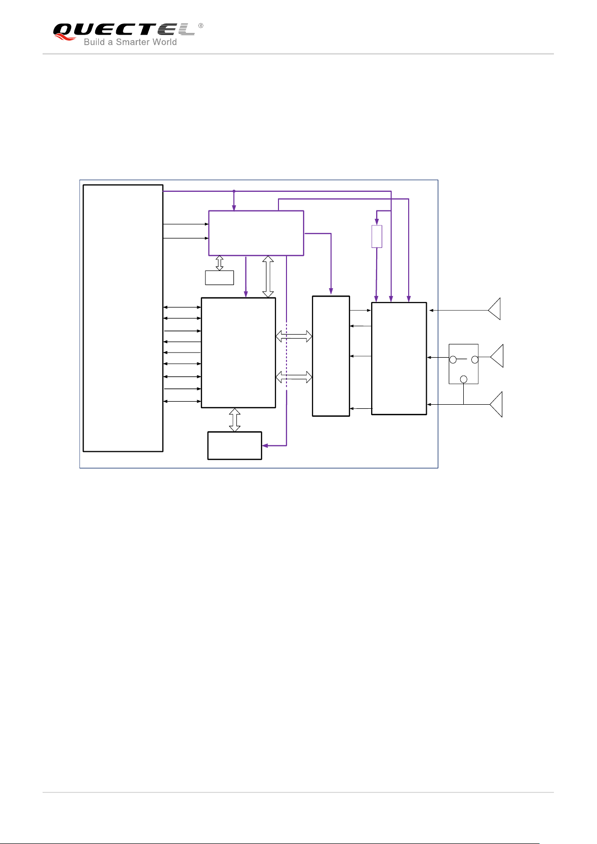
Baseband
PMIC
Transceiver
ANT_MAIN
ANT_GNSS
ET
VCC
RESET#
38.4MHz
XO
Control
QLINK
Control
Tx
PRx
DRx
PCI Express
M.2 Key
-B Interface
FULL_CARD_POWER_OFF#
W_DISABLE1#
USB2.0&USB3.0
(U)SIM1&(U)SIM2
WWAN_LED#
WAKE_ON_WAN#
NAND +
DDR2 SDRAM
PCM
W_DISABLE2#
GPIOs
Tx/Rx Blocks
ANT_DIV
PCIE*
EM12-G Hardware Design
2.3. Functional Diagram
The following figure shows a block diagram of EM12-G.
2.4. Evaluation Board
In order to help customers develop applications conveniently with EM12-G, Quectel supplies the
evaluation board (M.2 EVB), USB to RS-232 converter cable, USB type-C cable, earphone, antenna and
other peripherals to control or test the module. For more details, please refer to document [1].
EM12-G_Hardware_Design 15 / 62
Figure 1: Functional Diagram
LTE-A Module Series
“*” means under development.
NOTE
EM12-G Hardware Design
3 Application Interfaces
The physical connections and signal levels of EM12-G comply with PCI Express M.2 specifications. This
chapter mainly describes the definition and application of the following interfaces/signals/pins of EM12-G:
Power supply
(U)SIM interfaces
USB interface
PCIE interface*
PCM and I2C interfaces
Control and indicator signals
Tunable antenna control interface*
Configuration pins
EM12-G_Hardware_Design 16 / 62
LTE-A Module Series
PIN2
PIN74
BOT
PIN1
PIN75
TOP
P in Nam e No.
C O N F IG _ 2 75
GND 73
GND 71
C O N F IG _ 1 69
R E S E T # 67
ANTCTL3 65
ANTCTL2 63
ANTCTL1 61
ANTCTL0 59
GND 57
P C IE _R E FC LK+ 55
P C IE _R E FC LK- 53
GND 51
P C IE _R X + 49
P C IE _R X - 47
GND 45
P C IE _TX+ 43
P C IE _TX- 41
GND 39
USB 3 .0_ R X+ 37
USB 3 .0_ R X- 35
GND 33
USB 3 .0_ T X+ 31
USB 3 .0_ T X- 29
GND 27
D P R 25
W AKE_O N_W AN# 23
C O N F IG _ 0 21
Notc h
Notc h
Notc h
Notc h
GND 11
USB _ D M 9
USB _ D P 7
GND 5
GND 3
C O N F IG _ 3 1
No. P in Nam e
74 VC C
72 VC C
70 VC C
68 NC
66 US IM1_DE T
64 RE S E R VED
62 RE S E R VED
60 RE S E R VED
58 I2C_SC L
56 I2C _S D A
54 NC
52 NC
50 NC
48 US IM2_VD D
46 U S IM 2_R E S E T
44 U S IM2_CLK
42 US IM2_DATA
40 US IM2_DE T
38 NC
36 US IM1_VD D
34 US IM1_DATA
32 U S IM1_CLK
30 U S IM 1_R E S E T
28 P C M_SYNC
26 W _D IS AB LE 2#
24 PC M _O UT
22 PC M _ IN
20 P C M _C L K
Notc h
Notc h
Notc h
Notc h
10 W W AN_L E D #
8 W _ D IS AB L E 1 #
6
F ULL_C A R D _ P O W E R_OFF#
4 VC C
2 VC C
PIN11
PIN10
EM12-G Hardware Design
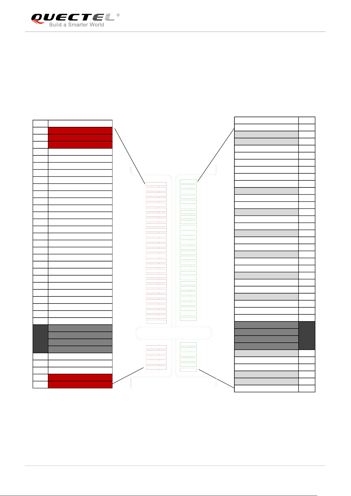
3.1. Pin Assignment
The following figure shows the pin assignment of EM12-G. The top side contains EM12-G module and
antenna connectors.
EM12-G_Hardware_Design 17 / 62
Figure 2: Pin Assignment
LTE-A Module Series
Type
Description
IO
Bidirectional
DI
Digital input
DO
Digital output
OD
Open drain
PI
Power input
PO
Power output
Pin
No.
M.2 Socket 2
WWAN Module
Pinout
EM12-G
Pin Name
I/O
Description
Comment
1
CONFIG_3
CONFIG_3
Not connected internally.
EM12-G is configured as
WWAN-USB 3.0.
2 3.3V
VCC
PI
Power supply
Vmin=3.135V
Vnorm=3.7V
Vmax=4.4V
3
GND
GND
Ground
4
3.3V
VCC
PI
Power supply
Vmin=3.135V
Vnorm=3.7V
Vmax=4.4V
5
GND
GND
Ground
6
FULL_CARD_
POWER_OFF#
FULL_CARD_
POWER_OFF#
DI
A signal to control power-on/-off
of the module. When it is at low
level, the module powers off.
When it is at high level, the
module powers on.
Pulled down
internally
EM12-G Hardware Design
3.2. Pin Description
The following tables show the pin definition and description of EM12-G on the 75-pin application.
Table 3: Definition of I/O Parameters
Table 4: Pin Description
EM12-G_Hardware_Design 18 / 62

LTE-A Module Series
7
USB_D+
USB_DP
IO
USB 2.0 differential data bus (+)
8
W_DISABLE1#
W_DISABLE1#
DI
Airplane mode control.
Active low.
1.8V/3.3V
power domain
9
USB_D-
USB_DM
IO
USB 2.0 differential data bus (-)
10
GPIO_9
WWAN_LED#
OD
It is an open collector and active
low signal.
It allows the module to provide
RF status indication via LED
devices provided by the system.
3.3V power
domain
11
GND
GND
Ground
12
Key
Notch
Notch
13
Key
Notch
Notch
14
Key
Notch
Notch
15
Key
Notch
Notch
16
Key
Notch
Notch
17
Key
Notch
Notch
18
Key
Notch
Notch
19
Key
Notch
Notch
20
GPIO_5
(AUDIO_0)
PCM_CLK
IO
PCM data bit clock. In master
mode, it is an output signal. In
slave mode, it is an input signal.
If unused, keep it open.
1.8V power
domain
21
CONFIG_0
CONFIG_0
Connected to GND internally.
EM12-G is configured as
WWAN-USB 3.0.
22
GPIO_6
(AUDIO_1)
PCM_IN
DI
PCM data input
1.8V power
domain
23
GPIO_11
(WOWWAN#)
WAKE_ON_
WAN#
OD
A signal to wake up the host.
It is an open collector and active
low signal.
1.8V power
domain
24
GPIO_7
(AUDIO_2)
PCM_OUT
DO
PCM data output
1.8V power
domain
25
DPR
DPR
DI
Dynamic power reduction.
High level by default.
1.8V power
domain
26
GPIO_10
(W_DISABLE2#)
W_DISABLE2#*
DI
GNSS enable control.
Active low.
1.8V/3.3V
power domain
27
GND
GND
Ground
28
GPIO_8
PCM_SYNC
IO
PCM data frame synchronization
1.8V power
EM12-G Hardware Design
EM12-G_Hardware_Design 19 / 62

LTE-A Module Series
(AUDIO_3)
signal
domain
29
USB3.0-TX-
USB3.0_TX-
DO
USB 3.0 transmit data (-)
30
UIM-RESET
USIM1_RESET
DO
(U)SIM1 card reset
1.8V/3.0V
power domain
31
USB3.0-TX+
USB3.0_TX+
DO
USB 3.0 transmit data (+)
32
UIM-CLK
USIM1_CLK
DO
(U)SIM1 card clock
1.8V/3.0V
power domain
33
GND
GND
Ground
34
UIM-DATA
USIM1_DATA
IO
(U)SIM1 card data
Pulled up to
USIM2_VDD
internally
35
USB3.0-RX-
USB3.0_RX-
DI
USB 3.0 receive data (-)
36
UIM-PWR
USIM1_VDD
PO
Power supply for (U)SIM1 card
1.8V/3.0V
power domain
37
USB3.0-RX+
USB3.0_RX+
DI
USB 3.0 receive data (+)
38
N/C
NC NC 39
GND
GND
Ground
40
GPIO_0
(SIM_DET2)
USIM2_DET
DI
(U)SIM2 card insertion detection
Pulled up
internally
41
PETn0
PCIE_TX-
DO
PCIE transmit data (-)
42
GPIO_1
(SIM_DAT2)
USIM2_DATA
IO
(U)SIM2 card data
Pulled up to
USIM2_VDD
internally
43
PETp0
PCIE_TX+
DO
PCIE transmit data (+)
44
GPIO_2
(SIM_CLK2)
USIM2_CLK
DO
(U)SIM2 card clock
1.8V/3.0V
power domain
45
GND
GND
Ground
46
GPIO_3
(SIM_RST2)
USIM2_RESET
DO
(U)SIM2 card reset
1.8V/3.0V
power domain
47
PERn0
PCIE_RX-
DI
PCIE receive data (-)
48
GPIO_4
(SIM_PWR2)
USIM2_VDD
PO
Power supply for (U)SIM2 card
1.8V/3.0V
power domain
49
PERp0
PCIE_RX+
DI
PCIE receive data (+)
50
PRRST#
PCIE_RST_N
DI
PCIE reset.
Active low.
3.3V power
domain
EM12-G Hardware Design
EM12-G_Hardware_Design 20 / 62

LTE-A Module Series
51
GND
GND
Ground
52
CLKREQ#
PCIE_CLKREQ_
N
IO
PCIE clock request.
Active low.
3.3V power
domain
53
REFCLKn
PCIE_REFCLK-
AI
PCIE reference clock(-)
54
PEWAKE#
PCIE_WAKE_N
IO
PCIE wake on host.
Active low.
3.3V power
domain
55
REFCLKp
PCIE_REFCLK+
AI
PCIE reference clock(+)
56
N/C
I2C_DATA
IO
I2C serial data.
Used for external codec.
57
GND
GND
Ground
58
N/C
I2C_CLK
DO
I2C serial clock.
Used for external codec.
59
ANTCTL0
ANTCTL0*
DO
Tunable antenna control.
1.8V power
domain
60
COEX3
RESERVED
Reserved
61
ANTCTL1
ANTCTL1*
DO
Tunable antenna control.
1.8V power
domain
62
COEX2
RESERVED
Reserved
63
ANTCTL2
ANTCTL2*
DO
Tunable antenna control.
1.8V power
domain
64
COEX1
RESERVED
Reserved
65
ANTCTL3
ANTCTL3*
DO
Tunable antenna control.
1.8V power
domain
66
SIM_DETECT
USIM1_DET
DI
(U)SIM1 card insertion detection
Pulled up
internally
67
RESET#
RESET#
DI
System reset. Active low.
68
SUSCLK (32kHz)
NC NC
69
CONFIG_1
CONFIG_1
Connected to GND internally.
EM12-G is configured as
WWAN-USB 3.0.
70
3.3V
VCC
PI
Power supply
Vmin=3.135V
Vnorm=3.7V
Vmax=4.4V
71
GND
GND
Ground
72
3.3V
VCC
PI
Power supply
Vmin=3.135V
Vnorm=3.7V
Vmax=4.4V
EM12-G Hardware Design
EM12-G_Hardware_Design 21 / 62
LTE-A Module Series
1. Keep all NC, reserved and unused pins unconnected.
2. “*” means under development.
VCC
Max Tx power
Min.3.135V
Ripple
Drop
Max Tx power
73
GND
GND
Ground
74
3.3V
VCC
PI
Power supply
Vmin=3.135V
Vnorm=3.7V
Vmax=4.4V
75
CONFIG_2
CONFIG_2
Not connected internally.
EM12-G is configured as
WWAN-USB 3.0.
Pin No.
Pin Name
I/O
Power Domain
Description
2, 4, 70, 72, 74
VCC
PI
3.135V~4.4V
3.7V typical DC supply
3, 5, 11, 27, 33,
39, 45, 51, 57, 71,
73
GND
Ground
NOTES
EM12-G Hardware Design
3.3. Power Supply
The following table shows pin definition of VCC pins and ground pins.
Table 5: Definition of VCC and GND Pins
3.3.1. Decrease Voltage Drop
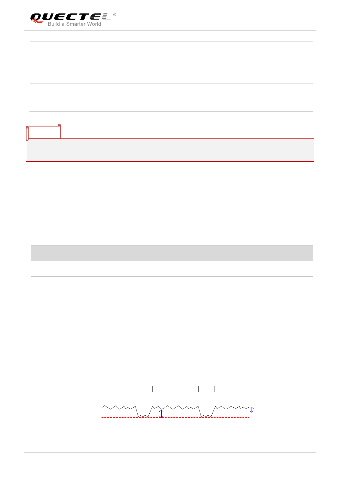
The power supply range of the module is from 3.135V to 4.4V. Please make sure that the input voltage will
never drop below 3.135V, otherwise the module will be powered off automatically. The following figure
shows the maximum voltage drop during radio transmission in 3G and 4G networks.
EM12-G_Hardware_Design 22 / 62

LTE-A Module Series
Module
VCC
VCC
C1
220uF
+
D1
5.1V
C2
1
uF
C3
100nF
C4
33pF
C5
10pF
EM12-G Hardware Design
Figure 3: Power Supply Limits during Radio Transmission
To decrease voltage drop, a bypass capacitor of about 220µF with low ESR (ESR=0.7Ω) should be used,
and a multi-layer ceramic chip capacitor (MLCC) array should also be reserved due to its ultra-low ESR. It
is recommended to use three ceramic capacitors (100nF, 33pF, 10pF) for composing the MLCC array,
and place these capacitors close to VCC pins. The main power supply from an external application has to
be a single voltage source. The width of VCC trace should be no less than 2mm. In principle, the longer
the VCC trace is, the wider it will be.
In addition, in order to get a stable power source, it is recommended to use a zener diode with reverse
zener voltage of 5.1V and dissipation power more than 0.5W. The following figure shows a reference
circuit of VCC.
Figure 4: Reference Circuit of VCC
3.3.2. Reference Design for Power Supply
Power design for the module is very important, as the performance of the module largely depends on the
power source. The power supply is capable of providing sufficient current up to 2A at least. If the voltage
drop between the input and output is not too high, it is suggested that an LDO should be used to supply
power for the module. If there is a big voltage difference between the input source and the desired output
(VCC), a buck converter is preferred to be used as the power supply.
The following figure shows a reference design for +5V input power source. The typical output of the power
supply is about 3.7V and the maximum load current is 3A.
EM12-G_Hardware_Design 23 / 62

LTE-A Module Series
LDO_IN
C1
C2
MIC29302WU U1
IN
OUT
EN
GND
ADJ
2 4
1
3
5
VCC
100nF
C3
470uF
C4
100nF
R2
100K 1%
51K 1%
R3
470uF
470R
51K
R4
R1
MCU_POWER
_ON/OFF
47K
4.7K
R5
R6
C5
C6
33pF
10pF
TVS
D1
In order to avoid damages to the internal flash, please do not switch off the power supply directly when
the module is working. It is suggested that the power supply can be cut off after pulling down
FULL_CARD_POWER_OFF# for about 100ms.
Pin Name
Pin No.
Description
DC Characteristics
Comment
FULL_CARD
_POWER_
OFF#
6
A signal to control power-on/-off
of the module. When it is at low
level, the module powers off.
When it is at high level, the
module powers on.
VIHmax=4.4V
VIHmin=0.7V
VILmax=0.5V
Pulled down
internally.
NOTE
EM12-G Hardware Design
Figure 5: Reference Design of Power Supply
3.4. Turn on and off Scenarios
3.4.1. Turn on the Module
Driving the FULL_CARD_POWER_OFF# pin to a high level will power on the module. The following table
shows the definition of FULL_CARD_POWER_OFF#.
Table 6: Definition of FULL_CARD_POWER_OFF# Pin
EM12-G_Hardware_Design 24 / 62

LTE-A Module Series
Module
Host
GND
GND
GPIO
FULL_CARD_POWER_OFF#
3.3V
Module
FULL_CARD_POWER_
OFF#
10K
3.3V
EM12-G Hardware Design
3.4.1.1. Turn on the Module Through GPIO Controlled FULL_CARD_POWER_OFF#
It is recommended to use a GPIO from host to control FULL_CARD_POWER_OFF#. A simple reference
circuit is illustrated in the following figure.
Figure 6: Turn on the Module Through GPIO Controlled FULL_CARD_POWER_OFF#
3.4.1.2. Turn on the Module Automatically
If FULL_CARD_POWER_OFF# is pulled up to 3.3V with a 5kΩ~10kΩ resistor, the module will be
powered on automatically when the power supply for VCC is applied, and will be powered off when the
power supply is removed.
A reference circuit is shown in the following figure.
Figure 7: Turn on the Module Automatically
EM12-G_Hardware_Design 25 / 62

LTE-A Module Series
VIL≤0.2V
VIH≥1.19V
VCC
FULL_CARD_POWER_OFF#
RESET#
Booting
Active
Module Status
NOTE
≥12.5s
OFF
Please make sure that VCC is stable before pulling down FUL_CARD_POWER_OFF# pin. The time
between them is no less than 30ms.
VCC
FULL_CARD_POWER_OFF#
RUNNING
OFF
Module
Status
ON
NOTE
EM12-G Hardware Design
The turn on scenario is illustrated in the following figure.
Figure 8: Timing of Turning on Module
3.4.2. Turn off the Module
3.4.2.1. Turn off the Module Through FULL_CARD_POWER_OFF#
Driving the FULL_CARD_POWER_OFF# pin to low will turn off the module.
The power-down scenario is illustrated in the following figure.
Figure 9: Timing of Turning off the Module Through FULL_CARD_POWER_OFF#
EM12-G_Hardware_Design 26 / 62
LTE-A Module Series
Reset pulse
RESET#
4.7K
47K
Pin Name
Pin No.
Description
DC Characteristics
Comment
RESET#
67
Reset the module
VIHmax=2.1V
VIHmin=1.3V
VILmax=0.5V
EM12-G Hardware Design
3.4.2.2. Turn off the Module via AT Command
The module can also be turned off by AT+QPOWD command. For more details about the command,
please refer to document [2].
3.5. Reset the Module
The RESET# pin is used to reset the module. The module can be reset by driving RESET# to a low level
voltage for 250ms~600ms.
Table 7: RESET# Pin Definition
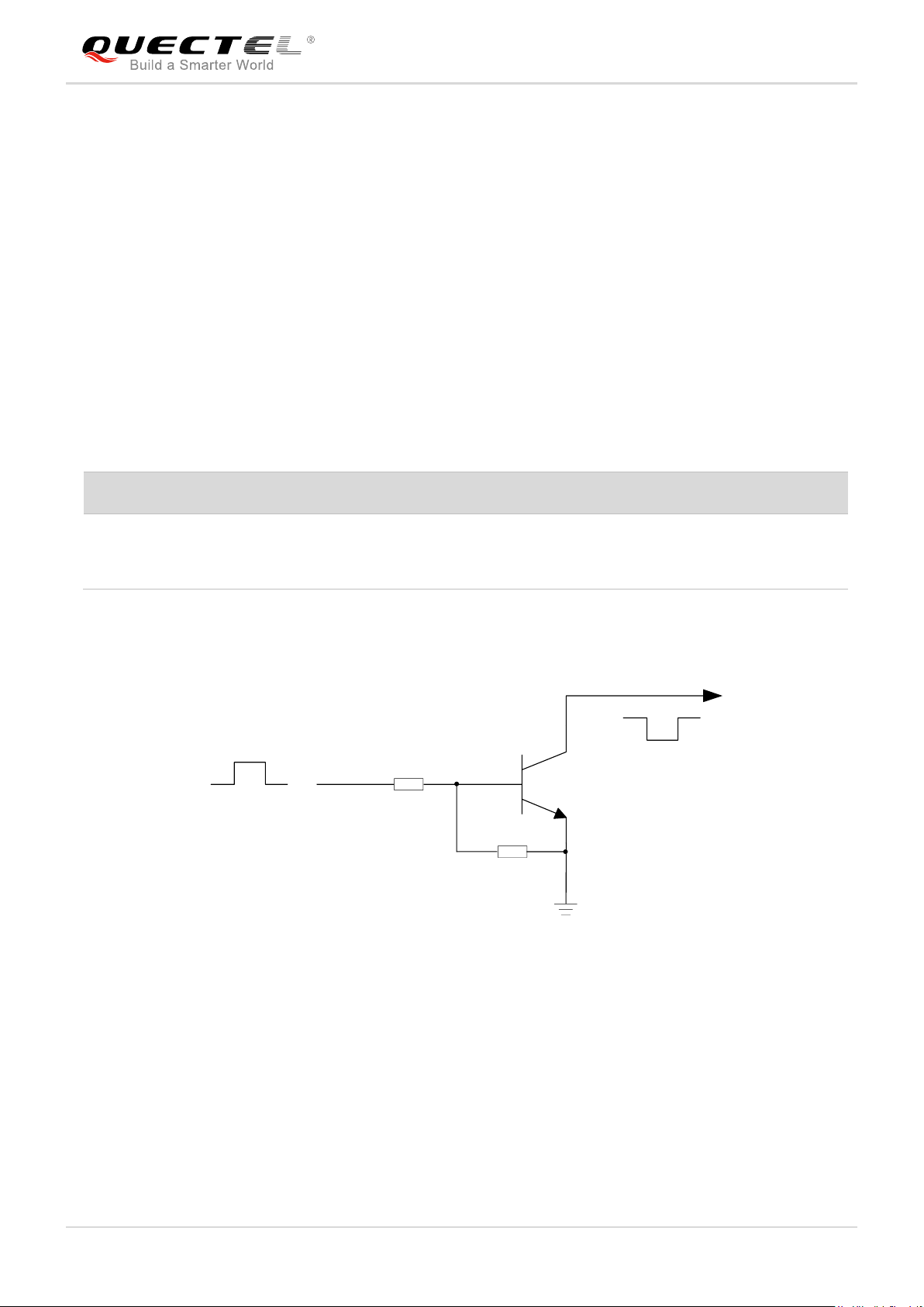
An open collector/collector driver or button can be used to control the RESET# pin.
Figure 10: Reference Circuit of RESET# by Using Driving Circuit
EM12-G_Hardware_Design 27 / 62

LTE-A Module Series
RESET#
S2
Close to S2
TVS
V
IL
≤0.5V
V
IH
≥1.3V
VCC
≥250ms
Resetting
Module
Status
Running
RESET#
Restart
≤600ms
Please ensure that there is no large capacitance on RESET# pin.
NOTE
EM12-G Hardware Design
Figure 11: Reference Circuit of RESET# by Using Button
The reset scenario is illustrated in the following figure.
Figure 12: Timing of Resetting Module
3.6. (U)SIM Interfaces
The (U)SIM interface circuitry meets ETSI and IMT-2000 requirements. Both 1.8V and 3.0V (U)SIM cards
are supported, and Dual SIM Single Standby* function is supported.
EM12-G_Hardware_Design 28 / 62

EM12-G Hardware Design
Pin Name
Pin No.
I/O
Description
Comment
USIM1_VDD
36
PO
Power supply for (U)SIM1
card
Either 1.8V or 3.0V is supported
by the module automatically.
USIM1_DATA
34
IO
Data signal of (U)SIM1 card
USIM1_CLK
32
DO
Clock signal of (U)SIM1 card
USIM1_RESET
30
DO
Reset signal of (U)SIM1 card
USIM1_DET
66
DI
(U)SIM1 card insertion
detection.
Active high.
Pulled up internally.
When (U)SIM1 card is present, it
is at high level.
When (U)SIM1 card is absent, it is
at low level.
USIM2_VDD
48
PO
Power supply for (U)SIM2
card
Either 1.8V or 3.0V is supported
by the module automatically.
USIM2_DATA
42
IO
Data signal of (U)SIM2 card
USIM2_CLK
44
DO
Clock signal of (U)SIM2 card
USIM2_RESET
46
DO
Reset signal of (U)SIM2 card
USIM2_DET
40
DI
(U)SIM2 card insertion
detection.
Active high.
Pulled up internally.
When (U)SIM2 card is present, it
is at high level.
When (U)SIM2 card is absent, it is
at low level.
Table 8: Pin Definition of (U)SIM Interfaces
LTE-A Module Series
EM12-G supports (U)SIM card hot-plug via the USIM_DET pin, which is a level trigger pin. The
USIM_DET is normally short-circuited to ground when (U)SIM card is not inserted. When the (U)SIM card
is inserted, the USIM_DET will change from low to high level. The rising edge will indicate insertion of the
(U)SIM card. When the (U)SIM card is removed, the USIM_DET will change from high to low level. This
falling edge will indicate the absence of the (U)SIM card.
The following figure shows a reference design of (U)SIM interface with normally short-circuited (U)SIM
card connector.
EM12-G_Hardware_Design 29 / 62

LTE-A Module Series
Module
USIM_VDD
USIM_RESET
USIM_CLK
USIM_DATA
USIM_DET
22R
22R
22R
100nF
(U)SIM Card Connector
GND
GND
33pF
33pF 33pF
VCC
RST
CLK
IO
VPP
GND
GND
USIM_VDD
15K
GND
CD SW
Module
USIM_VDD
USIM_RESET
USIM_CLK
USIM_DATA
USIM_DET
22R
22R
22R
100nF
(U)SIM Card Connector
GND
33pF
33pF 33pF
VCC
RST
CLK
IO
VPP
GND
GND
USIM_VDD
15K
GND
CD
1.8V
4.7K
33K
SW
EM12-G Hardware Design
Figure 13: Reference Circuit of Normally Short-Circuited (U)SIM Card Connector
Normally Short-Circuited (U)SIM Card Connector:
When the (U)SIM is absent, CD is short-circuited to SW and USIM_DET is at low level.
When the (U)SIM is inserted, CD is open to SW and USIM_DET is at high level.
The following figure shows a reference design of (U)SIM interface with normally open (U)SIM card
connector.
Figure 14: Reference Circuit of Normally Open (U)SIM Card Connector
Normally Open (U)SIM Card Connector:
When the (U)SIM is absent, CD is open to SW and USIM_DET is at low level.
When the (U)SIM is inserted, CD is short-circuited to SW and USIM_DET is at high level.
EM12-G_Hardware_Design 30 / 62
LTE-A Module Series
Module
USIM_VDD
USIM_GND
USIM_RESET
USIM_CLK
USIM_DATA
22R
22R
22R
100nF
(U)SIM Card Connector
GND
33pF 33pF 33pF
VCC
RST
CLK IO
VPP
GND
GND
15K
USIM_VDD
“*” means under development.
NOTE
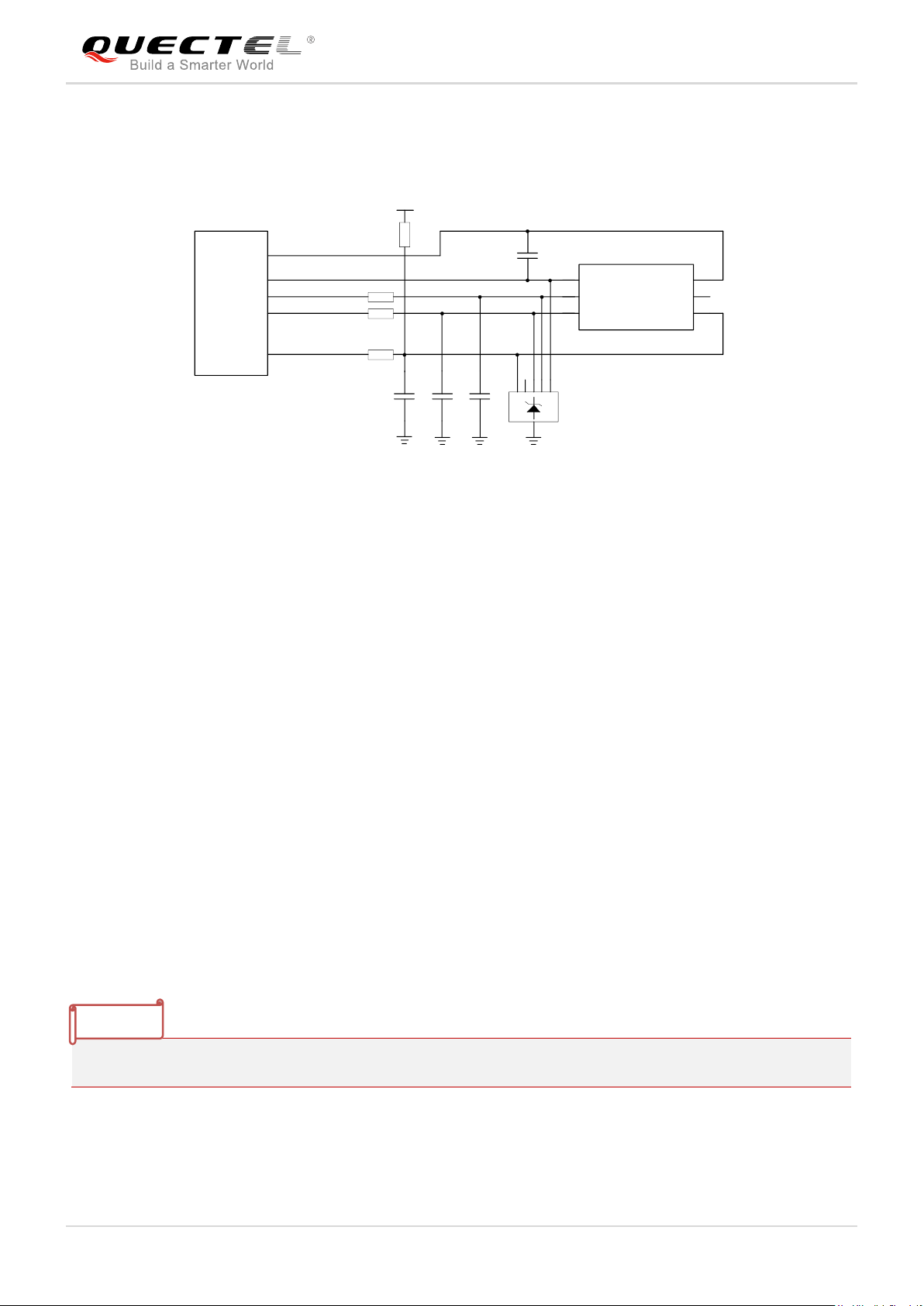
EM12-G Hardware Design
If (U)SIM card detection function is not needed, please keep USIM_DET unconnected. A reference circuit
for (U)SIM card interface with a 6-pin (U)SIM card connector is illustrated in the following figure.
Figure 15: Reference Circuit of a 6-Pin (U)SIM Card Connector
In order to enhance the reliability and availability of the (U)SIM card in customers’ applications, please
follow the criteria below in (U)SIM circuit design:
Keep placement of (U)SIM card connector as close as possible to the module. Keep the trace length
as less than 200mm as possible.
Keep (U)SIM card signals away from RF and VCC traces.
Assure the ground between the module and the (U)SIM card connector short and wide. Keep the
trace width of ground and USIM_VDD no less than 0.5mm to maintain the same electric potential.
To avoid cross-talk between USIM_DATA and USIM_CLK, keep them away from each other and
shield them with surrounded ground.
In order to offer good ESD protection, it is recommended to add a TVS diode array with parasitic
capacitance not exceeding 10pF. The 22Ω resistors should be added in series between the module
and the (U)SIM card connector so as to suppress EMI spurious transmission and enhance ESD
protection. The 33pF capacitors are used to filter out RF interference. Please note that the (U)SIM
peripheral circuit should be close to the (U)SIM card connector.
The pull-up resistor on USIM_DATA line can improve anti-jamming capability when long layout trace
and sensitive occasion are applied, and should be placed close to the (U)SIM card connector.
EM12-G_Hardware_Design 31 / 62

LTE-A Module Series
Pin No.
Pin Name
I/O
Description
Comment
7
USB_DP
IO
USB 2.0 differential data bus (+)
Require differential impedance
of 90Ω
9
USB_DM
IO
USB 2.0 differential data bus (-)
29
USB3.0_TX-
DO
USB 3.0 transmit data (-)
Require differential impedance
of 90Ω
31
USB3.0_TX+
DO
USB 3.0 transmit data (+)
35
USB3.0_RX-
DI
USB 3.0 receive data (-)
Require differential impedance
of 90Ω
37
USB3.0_RX+
DI
USB 3.0 receive data (+)
EM12-G Hardware Design
3.7. USB Interface
EM12-G provides one integrated Universal Serial Bus (USB) interface which complies with the USB
3.0/2.0 specifications and supports super speed (5Gbps) on USB 3.0, high speed (480 Mbps) and full
speed (12 Mbps) modes on USB 2.0. The USB interface is used for AT command communication, data
transmission, GNSS NMEA output, software debugging, firmware upgrade and voice over USB*.
The following table shows the pin definition of USB interface.
Table 9: Pin Definition of USB Interface
For more details about the USB 2.0 & 3.0 specifications, please visit http://www.usb.org/home.
The USB interface is recommended to be reserved for firmware upgrade in customers’ designs. The
following figure shows a reference circuit of USB 2.0 & USB 3.0 interface.
EM12-G_Hardware_Design 32 / 62
LTE-A Module Series
GND
USB3.0_TX-
USB3.0_TX+
GND
USB3.0_RX-
USB3.0_RX+
USB3.0_RX-
USB3.0_RX+
USB3.0_TX-
USB3.0_TX+
C3
C4
USB_DP
USB_DM
R1
R2
0R
0R
USB_DM
USB_DP
C1
C2
ESD Array
100nF
100nF
100nF
100nF
Module
MCU
R3
R4
NM_0R
NM_0R
Test Points
Minimize these stubs
EM12-G Hardware Design
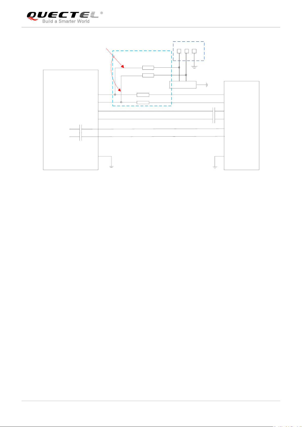
Figure 16: Reference Circuit of USB 2.0 & 3.0 Interface
In order to ensure the integrity of USB 2.0 & 3.0 data line signal, R1/R2/R3/R4 components must be
placed close to the module, capacitors C1 and C2 have been placed inside the module, capacitors C3
and C4 must be placed close to the MCU, and these components should be placed close to each other.
In order to ensure the USB interface design corresponding with USB 2.0 & 3.0 specifications, please
comply with the following principles:
It is important to route the USB 2.0 & 3.0 signal traces as differential pairs with total grounding.
1) For USB 2.0 routing traces, the trace impedance of the differential pair should be 90Ω, and the
trace length difference between the differential pair should be less than 2mm.
2) For USB 3.0 routing traces, the trace impedance of Tx and Rx differential pairs should be 90Ω,
and the trace length difference between Tx and Rx differential pairs should be less than
0.7mm.
Do not route signal traces under crystals, oscillators, magnetic devices or RF signal traces. It is
important to route the USB 2.0 & 3.0 differential traces in inner-layer with ground shielding on not
only upper and lower layers but also right and left sides.
If USB connector is used, please keep the ESD protection components as close as possible to the
USB connector. Pay attention to the influence of junction capacitance of ESD protection components
on USB 2.0 & 3.0 data lines. The capacitance value of ESD protection components should be less
than 2.0pF for USB 2.0, and less than 0.4pF for USB 3.0.
If possible, reserve a 0R resistor on USB_DP and USB_DM lines, respectively.
EM12-G_Hardware_Design 33 / 62

LTE-A Module Series
“*” means under development.
NOTE
EM12-G Hardware Design
3.8. PCIE Interface
Under development
3.9. PCM and I2C Interfaces
EM12-G supports audio communication via Pulse Code Modulation (PCM) digital interface and I2C
interface.
The PCM interface supports the following modes:
Primary mode (short frame synchronization, works as both master and slave)
Auxiliary mode (long frame synchronization, works as master only)
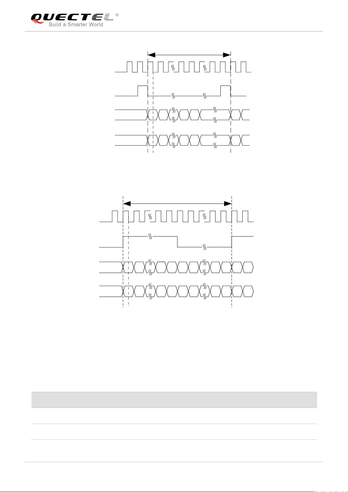
In primary mode, the data is sampled on the falling edge of the PCM_CLK and transmitted on the rising
edge. The PCM_SYNC falling edge represents the MSB. In this mode, the PCM interface supports
256kHz, 512kHz, 1024kHz or 2048kHz PCM_CLK at 8kHz PCM_SYNC, and also supports 4096kHz
PCM_CLK at 16kHz PCM_SYNC.
In auxiliary mode, the data is sampled on the falling edge of the PCM_CLK and transmitted on the rising
edge. The PCM_SYNC rising edge represents the MSB. In this mode, PCM interface operates with a
256kHz PCM_CLK and an 8kHz, 50% duty cycle PCM_SYNC only.
EM12-G supports 16-bit linear data format. The following figures show the primary mode’s timing
relationship with 8kHz PCM_SYNC and 2048kHz PCM_CLK, as well as the auxiliary mode’s timing
relationship with 8kHz PCM_SYNC and 256kHz PCM_CLK.
EM12-G_Hardware_Design 34 / 62
LTE-A Module Series
PCM_CLK
PCM_SYNC
PCM_OUT
MSB
LSB
MSB
125us
1 2 256255
PCM_IN
MSB
LSBMSB
PCM_CLK
PCM_SYNC
PCM_OUT
MSB
LSB
PCM_IN
125us
MSB
1 2 3231
LSB
Pin Name
Pin No.
I/O
Description
Comment
PCM_IN
22
DI
PCM data input
1.8V power domain.
PCM_OUT
24
DO
PCM data output
1.8V power domain.
EM12-G Hardware Design
Figure 17: Primary Mode Timing
The following table shows the pin definition of PCM and I2C interfaces which can be applied on audio
codec design.
Table 10: Pin Definition of PCM and I2C Interfaces
EM12-G_Hardware_Design 35 / 62
Figure 18: Auxiliary Mode Timing

LTE-A Module Series
PCM_SYNC
28
IO
PCM data frame
synchronization signal
1.8V power domain.
PCM_CLK
20
IO
PCM data bit clock
1.8V power domain.
In master mode, it is an output
signal. In slave mode, it is an
input signal.
If unused, keep it open.
I2C_SCL
58
DO
I2C serial clock
Used for external codec.
Require an external pull-up to
1.8V.
I2C_SDA
56
IO
I2C serial data
PCM_IN
PCM_OUT
PCM_SYNC
PCM_CLK
I2C_SCL
I2C_SDA
Module
1.8V
4.7K
BCLK
LRCK
DAC
ADC
SCL
SDA
BIAS
MICBIAS
INP
INN
LOUTP
LOUTN
Codec
4.7K
1. It is recommended to reserve an RC (R=22Ω, C=22pF) circuit on the PCM lines, especially for
PCM_CLK.
2. EM12-G works as a master device pertaining to I2C interface.
NOTES
EM12-G Hardware Design
The clock and mode can be configured by AT command, and the default configuration is master mode
using short frame synchronization format with 2048kHz PCM_CLK and 8kHz PCM_SYNC. Please refer to
document [2] for details about AT+QDAI command.
The following figure shows a reference design of PCM interface with an external codec IC.
Figure 19: Reference Circuit of PCM Application with Audio Codec
3.10. Control and Indicator Signals
The following table shows the pin definition of control and indicator signals.
EM12-G_Hardware_Design 36 / 62

LTE-A Module Series
“*” means under development.
Pin No.
Pin Name
I/O
Power Domain
Description
10
WWAN_LED#
OD
3.3V
It is an open collector and active low
signal.
It is used to indicate the RF status of
the module.
23
WAKE_ON_WAN#
OD
1.8V
A signal to wake up the host.
It is an open collector and active low
signal.
8
W_DISABLE1#
DI
1.8V/3.3V
Airplane mode control. Active low.
26
W_DISABLE2#*
DI
1.8V/3.3V
GNSS enable control. Active low.
25
DPR
DI
1.8V
Dynamic power reduction. High level
by default.
W_DISABLE1# Level
AT Commands
RF Function Status
High Level
AT+CFUN=1
Enabled
High Level
AT+CFUN=0
AT+CFUN=4
Disabled
Low Level
AT+CFUN=0
AT+CFUN=1
AT+CFUN=4
Disabled
NOTE
EM12-G Hardware Design
Table 11: List of Control and Indicator Signals
3.10.1. W_DISABLE1# Signal
EM12-G provides a W_DISABLE1# signal to disable or enable airplane mode through hardware
operation. The W_DISABLE1# pin is pulled up by default. Driving it to low level will let the module enter
into airplane mode.
In airplane mode, the RF function will be disabled. The RF function can also be enabled or disabled
through software AT commands. The following table shows the RF function status of the module.
Table 12: RF Function Status
EM12-G_Hardware_Design 37 / 62
LTE-A Module Series
WWAN_LED#
VCC
R
WWAN_LED# Level
Description
Low Level (LED ON)
RF function is turned on
High Level (LED OFF)
RF function is turned off if any of the following circumstances occurs:
The (U)SIM card is not powered
W_DISABLE1# signal is at low level (airplane mode enabled).
AT+CFUN=4 (RF function disabled)
WAKE_ON_WAN# State
Module Operation Status
Output a 1s low level pulse signal
Call/SMS/Data is incoming (to wake up the host)
Always at high level
Idle/Sleep
EM12-G Hardware Design
3.10.2. WWAN_LED# Signal
The WWAN_LED# signal is used to indicate the RF status of the module, and its typical current
consumption is up to 40mA.
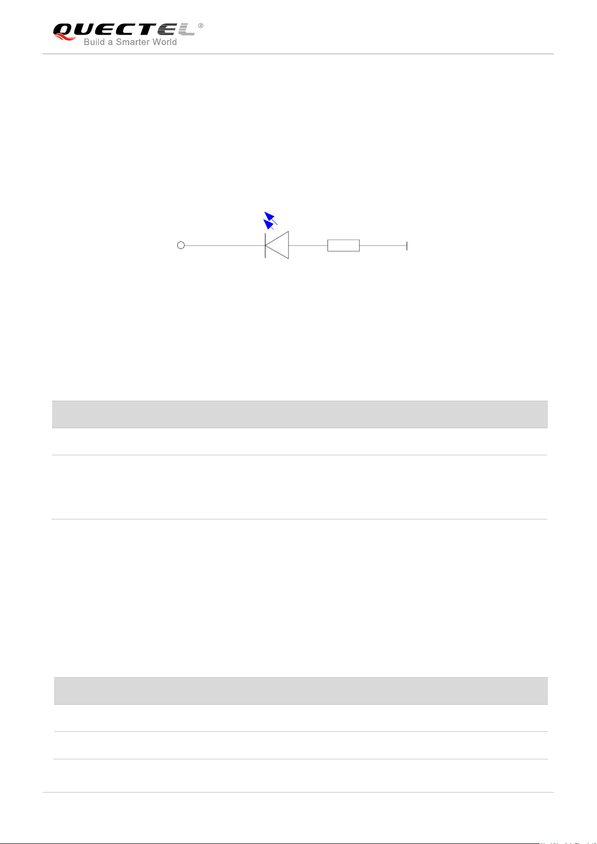
In order to reduce the current consumption of the LED, a resistor must be placed in series with the LED,
as illustrated in the figure below. The LED is ON when the WWAN_LED# signal is at a low voltage level.
Figure 20: WWAN_LED# Signal Reference Circuit Diagram
The following table shows the RF status indicated by WWAN_LED# signal.
Table 13: Network Status Indications of WWAN_LED# Signal
3.10.3. WAKE_ON_WAN# Signal
The WAKE_ON_WAN# signal is an open collector signal, which requires a pull-up resistor on the host.
When a URC returns, a 1s low level pulse signal will be outputted to wake up the host. The module
operation status indicated by WAKE_ON_WAN# is shown as below.
Table 14: State of the WAKE_ON_WAN# Signal
EM12-G_Hardware_Design 38 / 62

LTE-A Module Series
Wake up the host
1s
High
Low
(external pull-up)
Module
Host
WAKE_ON_WAN#
10K
VCC from the Host
Please refer to document [2] for more details about AT+QCFG="sarcfg" command.
DPR Level
Function
High/Floating
Max transmitting power will NOT be backed off
Low
Max transmitting power will be backed off by executing AT+QCFG="sarcfg"
command
NOTE
EM12-G Hardware Design
Figure 21: WAKE_ON_WAN# Behavior
Figure 22: WAKE_ON_WAN# Signal Reference Circuit Design
3.10.4. DPR Signal
EM12-G provides a DPR (Dynamic Power Reduction) signal for body SAR (Specific Absorption Rate)
detection. The signal is sent by a host system proximity sensor to EM12-G module to provide an input
trigger which will reduce the output power in the radio transmission.
Table 15: Function of the DPR Signal
EM12-G_Hardware_Design 39 / 62

LTE-A Module Series
Pin Name
Pin No.
I/O
Description
Comment
ANTCTL0*
59
DO
Tunable antenna control
1.8V power domain
ANTCTL1*
61
DO
Tunable antenna control
1.8V power domain
ANTCTL2*
63
DO
Tunable antenna control
1.8V power domain
ANTCTL3*
65
DO
Tunable antenna control
1.8V power domain
“*” means under development.
Pin No.
Pin Name
I/O
Power Domain
Description
21
CONFIG_0
0 Connected to GND internally.
69
CONFIG_1
0 Connected to GND internally.
75
CONFIG_2
0 NC 1 CONFIG_3
0 NC
NOTE
EM12-G Hardware Design
3.11. Tunable Antenna Control Interface*
ANTCTL[0:3] signals are used for tunable antenna control and should be routed to an appropriate
antenna control circuitry.
More details about the interface will be added in the future version of the document.
Table 16: Pin Definition of Tunable Antenna Control Interface*
3.12. Configuration Pins
EM12-G provides 4 configuration pins, and it is configured as WWAN-USB 3.0 2.
Table 17: Pin Definition of Configuration Pins
The 4 pins on EM12-G module are defined as below:
EM12-G_Hardware_Design 40 / 62

Config_0
(Pin 21)
Config_1
(Pin 69)
Config_2
(Pin 75)
Config_3
(Pin 1)
Module Type and
Main Host Interface
Port
Configuration
GND
GND
NC
NC
WWAN-USB 3.0
2
Table 18: List of Configuration Pins
LTE-A Module Series
EM12-G Hardware Design
EM12-G_Hardware_Design 41 / 62

LTE-A Module Series
EM12-G Hardware Design
4 GNSS Receiver
4.1. General Description
EM12-G includes a fully integrated global navigation satellite system solution that supports Gen9C-Lite of
Qualcomm (GPS, GLONASS, BeiDou Galileo and QZSS).
EM12-G supports standard NMEA-0183 protocol, and outputs NMEA sentences at 1Hz data update rate
via USB interface by default.
By default, EM12-G GNSS engine is switched off. It has to be switched on via AT command. For more
details about GNSS engine technology and configurations, please refer to document [3].
EM12-G_Hardware_Design 42 / 62

LTE-A Module Series
EM12-G Hardware Design
5 Antenna Interfaces
EM12-G provides a main antenna interface, an Rx-diversity antenna interface which is used to resist the
fall of signals caused by high speed movement and multipath effect, and a GNSS antenna interface. The
antenna ports have an impedance of 50Ω.
5.1. Main/Rx-diversity Antenna Interfaces
The main/Rx-diversity/GNSS antenna interfaces are shown as below.
Figure 23: Antenna Interfaces on the Module
EM12-G_Hardware_Design 43 / 62

EM12-G Hardware Design
3GPP Band
Transmit
Receive
Unit
WCDMA B1
1920~1980
2110~2170
MHz
WCDMA B2
1850~1910
1930~1990
MHz
WCDMA B3
1710~1785
1805~1880
MHz
WCDMA B4
1710~1755
2110~2155
MHz
WCDMA B5
824~849
869~894
MHz
WCDMA B8
880~915
925~960
MHz
WCDMA B9
1750~1785
1845~1880
MHz
WCDMA B19
830~845
875~890
MHz
LTE B1
1920~1980
2110~2170
MHz
LTE B2
1850~1910
1930~1990
MHz
LTE B3
1710~1785
1805~1880
MHz
LTE B4
1710~1755
2110~2155
MHz
LTE B5
824~849
869~894
MHz
LTE B7
2500~2570
2620~2690
MHz
LTE B8
880~915
925~960
MHz
LTE B9
1749.9~1784.9
1844.9~1879.9
MHz
LTE B12
699~716
729~746
MHz
LTE B13
777~787
746~756
MHz
LTE B14
788~798
758~768
MHz
LTE B17
704~716
734~746
MHz
LTE B18
815~830
860~875
MHz
LTE B19
830~845
875~890
MHz
5.1.1. Operating Frequency
Table 19: EM12-G Operating Frequencies
LTE-A Module Series
EM12-G_Hardware_Design 44 / 62

LTE-A Module Series
Type
Frequency
Unit
GPS/Galileo
1575.42±1.023
MHz
GLONASS
1597.5~1605.8
MHz
BeiDou
1561.098±2.046
MHz
LTE B20
832~862
791~821
MHz
LTE B21
1447.9~1462.9
1495.9~1510.9
MHz
LTE B25
1850~1915
1930~1995
MHz
LTE B26
814~849
859~894
MHz
LTE B28
703~748
758~803
MHz
LTE B29
/
717~728
MHz
LTE B30
2305~2315
2350~2360
MHz
LTE B32
/
1452~1496
MHz
LTE B38
2570~2620
2570~2620
MHz
LTE B39
1880~1920
1880~1920
MHz
LTE B40
2300~2400
2300~2400
MHz
LTE B41
2496~2690
2496~2690
MHz
LTE B66
1710~1780
2110~2200
MHz
EM12-G Hardware Design
5.2. GNSS Antenna Interface
The following table shows frequency specification of GNSS antenna interface.
Table 20: GNSS Frequency
EM12-G_Hardware_Design 45 / 62

LTE-A Module Series
Type
Requirements
GNSS 1)
Frequency range: 1559MHz ~ 1609MHz
Polarization: RHCP or linear
VSWR: < 2 (Typ.)
Passive antenna gain: > 0dBi
WCDMA/LTE
VSWR: ≤ 2
Efficiency: > 30%
Max Input Power: 50W
Input Impedance: 50Ω
Cable insertion loss: <1dB
(WCDMA B5/B8/B19,
LTE B5/B8/B12/B13/B14/B17/B18/B19/B20/B26/B28/B29)
Cable insertion loss: <1.5dB
(WCDMA B1/B2/B3/B4/B9, LTE B1/B2/B3/B4/B9/B21/B25/B32/B39/B66)
Cable insertion loss <2dB
(LTE B7/B30/B38/B40/B41)
1)
It is recommended to use a passive GNSS antenna when LTE B13 or B14 is supported, as the use of
active antenna may generate harmonics which will affect the GNSS performance.
NOTE
EM12-G Hardware Design
5.3. Antenna Installation
5.3.1. Antenna Requirements
The following table shows the requirements on main antenna, Rx-diversity antenna and GNSS antenna.
Table 21: Antenna Requirements
5.3.2. Recommended RF Connector for Antenna Installation
EM12-G is mounted with standard 2mm × 2mm receptacle RF connectors for convenient antenna
connection. The connector dimensions are illustrated below:
EM12-G_Hardware_Design 46 / 62
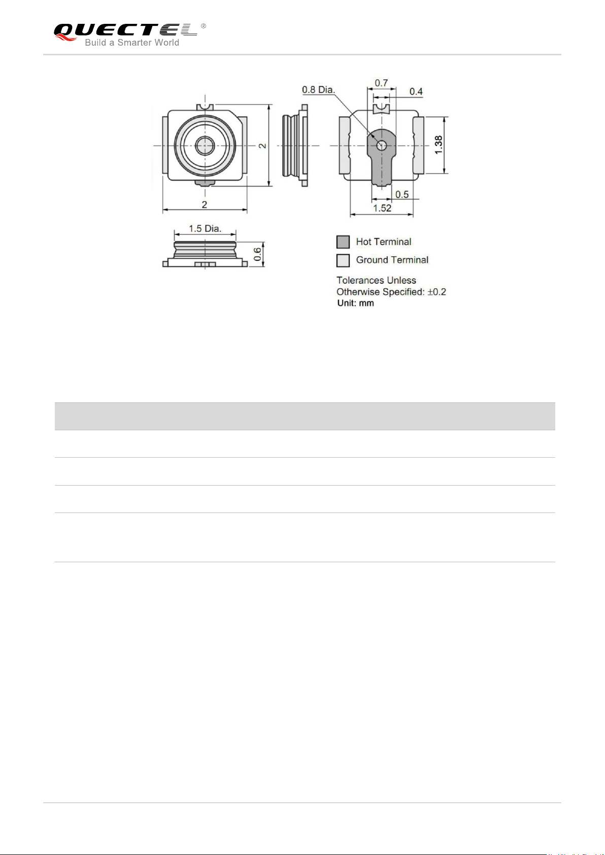
LTE-A Module Series
Item
Specification
Nominal Frequency Range
DC to 6GHz
Nominal Impedance
50Ω
Temperature Rating
-40°C to +85°C
Voltage Standing Wave Ratio (VSWR)
Meet the requirements of:
Max 1.3 (DC~3GHz)
Max 1.45 (3GHz~6GHz)
EM12-G Hardware Design
Figure 24: EM12-G RF Connector Dimensions (Unit: mm)
Table 22: Major Specifications of the RF Connector
The receptacle RF connector used in conjunction with EM12-G will accept two types of mating plugs that
will meet a maximum height of 1.2mm using a Ø0.81mm coaxial cable or a maximum height of 1.45mm
utilizing a Ø1.13mm coaxial cable.
The following figure shows the specifications of mating plugs using Ø0.81mm coaxial cables.
EM12-G_Hardware_Design 47 / 62
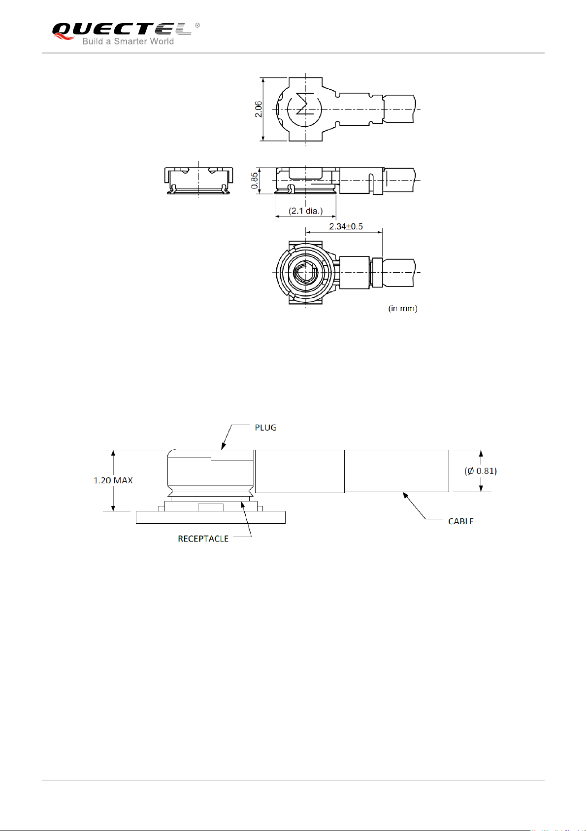
LTE-A Module Series
EM12-G Hardware Design
Figure 25: Specifications of Mating Plugs Using Ø0.81mm Coaxial Cables
The following figure illustrates the connection between the receptacle RF connector on EM12-G and the
mating plug using a Ø0.81mm coaxial cable.
Figure 26: Connection between RF Connector and Mating Plug Using Ø0.81mm Coaxial Cable
The following figure illustrates the connection between the receptacle RF connector on EM12-G and the
mating plug using a Ø1.13mm coaxial cable.
EM12-G_Hardware_Design 48 / 62
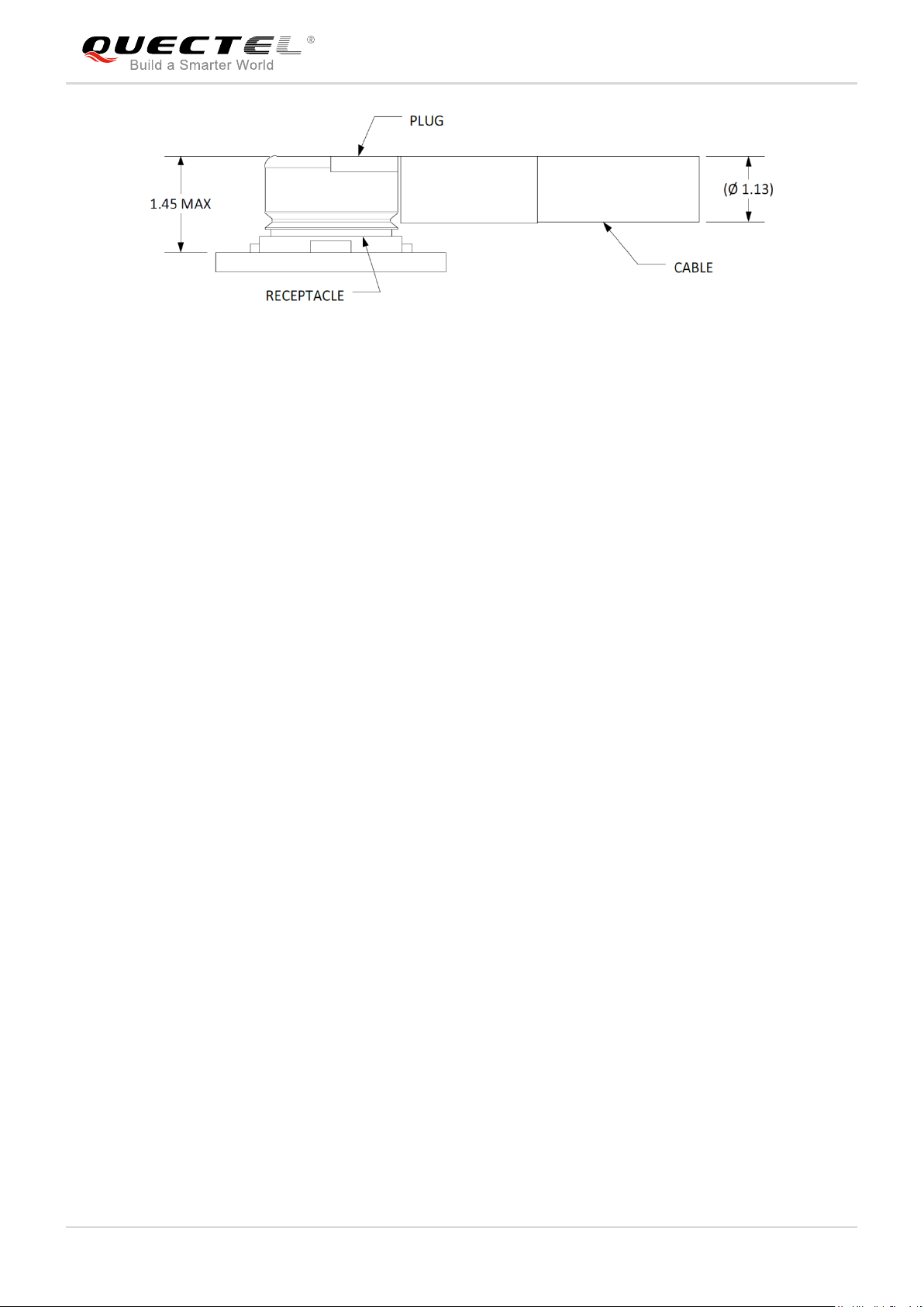
LTE-A Module Series
EM12-G Hardware Design
Figure 27: Connection between RF Connector and Mating Plug Using Ø1.13mm Coaxial Cable
EM12-G_Hardware_Design 49 / 62

LTE-A Module Series
Parameter
Min.
Max.
Unit
VCC
-0.3
4.7
V
Voltage at Digital Pins
-0.3
2.3
V
Parameter
Description
Min.
Typ.
Max.
Unit
VCC
Power Supply
3.135
3.7
4.4
V
EM12-G Hardware Design
6 Electrical, Reliability and Radio
Characteristics
6.1. Absolute Maximum Ratings
Absolute maximum ratings for power supply and voltage on digital and analog pins of the module are
listed in the following table.
Table 23: Absolute Maximum Ratings
6.2. Power Supply Requirements
The typical input voltage of EM12-G is 3.7V, as specified by PCIe M.2 Electromechanical Spec Rev1.0.
The following table shows the power supply requirements of EM12-G.
Table 24: Power Supply Requirements
EM12-G_Hardware_Design 50 / 62
6.3. I/O Requirements
1)
V
DD18
refers to I/O power domain.
Parameter
Min.
Typ.
Max.
Unit
Operation Temperature Range 1)
-30
+25
+70
ºC
Extended Temperature Range 2)
-40 +85
ºC
Storage temperature Range
-40 +90
ºC
1.
1)
Within operation temperature range, the module is 3GPP compliant.
2.
2)
Within extended temperature range, the module remains the ability to establish and maintain a
voice, SMS, data transmission, emergency call, etc. There is no unrecoverable malfunction. There
are also no effects on radio spectrum and no harm to radio network. Only one or more parameters
like P
out
might reduce in their value and exceed the specified tolerances. When the temperature
returns to the normal operating temperature levels, the module will meet 3GPP specifications again.
Parameter
Description
Min.
Max.
Unit
VIH
Input high voltage
0.7 × V
DD18
1)
V
DD18
+0.3
V
VIL
Input low voltage
-0.3
0.3 × V
DD18
V
VOH
Output high voltage
V
DD18
-0.5
V
DD18
V
VOL
Output low voltage
0
0.4
V
NOTES
NOTE
Table 25: I/O Requirements
LTE-A Module Series
EM12-G Hardware Design
6.4. Operation and Storage Temperatures
Table 26: Operation and Storage Temperatures
EM12-G_Hardware_Design 51 / 62
LTE-A Module Series
Frequency
Max.
Min.
WCDMA bands
24dBm+1/-3dB
<-50dBm
LTE- FDD bands
23dBm±2dB
<-40dBm
LTE-TDD bands
23dBm±2dB
<-40dBm
Frequency
Primary (Typ.)
Diversity (Typ.)
SIMO
1)
(Typ.)
3GPP (SIMO)
WCDMA B1
-109.5
/ / -106.7dBm
WCDMA B2
-109.5
/ / -104.7dbm
WCDMA B3
-109.5
/ / -103.7dbm
WCDMA B4
-109.0
/ / -106.7dBm
WCDMA B5
-110.5
/ / -104.7dbm
WCDMA B8
-110.5
/ / -103.7dBm
WCDMA B9
-109.5
/ / -105.7dBm
WCDMA B19
-110.5
/ / -106.7dBm
LTE-FDD B1 (10M)
-96.5
-96.0
-98.5dbm
-96.3dBm
EM12-G Hardware Design
6.5. Current Consumption(TBD)
6.6. RF Output Power
The following table shows the RF output power of EM12-G module.
Table 27: RF Output Power
6.7. RF Receiving Sensitivity
The following tables show conducted RF receiving sensitivity of EM12-G module.
Table 28: EM12-G Conducted RF Receiving Sensitivity(PRX、DRX TBD)
EM12-G_Hardware_Design 52 / 62

LTE-A Module Series
LTE-FDD B2 (10M)
-97.5
-97.0
-99.5dbm
-94.3dBm
LTE-FDD B3 (10M)
-97.0
-96.5
-99.0dbm
-93.3dBm
LTE-FDD B4 (10M)
-97.0
-96.0
-99.0dBm
-96.3dBm
LTE-FDD B5 (10M)
-98.5
-98.5
-100.5dBm
-94.3dBm
LTE-FDD B7 (10M)
-96.5
-96.0
-98.5dBm
-94.3dBm
LTE-FDD B8 (10M)
-98.0
-98.0
-101.5dBm
-93.3dBm
LTE-FDD B9(10M)
-97.5
-97.5
-100.0dBm
-95.3dBm
LTE-FDD B12 (10M)
-98.5
-99.0
-101.5dBm
-93.3dBm
LTE-FDD B13 (10M)
-99.0
-99.0
-101.0dBm
-93.3dBm
LTE-FDD B14 (10M)
-97.0
-97.5
-100.0dBm
-93.3dBm
LTE-FDD B17 (10M)
-99.0
-99.0
-101.0dBm
-93.3dBm
LTE-FDD B18 (10M)
-99.0
-99.0
-101.0dBm
-96.3dBm
LTE-FDD B19 (10M)
-98.5
-98.5
-100.5dBm
-96.3dBm
LTE-FDD B20 (10M)
-98.5
-98.5
-100.5dBm
-93.3dBm
LTE-FDD B21 (10M)
-96.0
-96.0
-98.0dBm
-96.3dBm
LTE-TDD B25 (10M)
-96.5
-97.0
-99.0dBm
-92.8dBm
LTE-TDD B26 (10M)
-99.0
-98.5
-100.5dBm
-93.8dBm
LTE-TDD B28 (10M)
-98.0
-99.0
-100.5dBm
-94.8dBm
LTE-TDD B29 (10M)
/
/
/
/
LTE-TDD B30 (10M)
-97.0
-95.0
-98.0dBm
-95.3dBm
LTE-TDD B32 (10M)
/
/
/
/
LTE-TDD B38 (10M)
-96.5
-96.0
-98.0dBm
-96.3dBm
LTE-TDD B39 (10M)
-97.0
-97.5
-99.5dBm
-96.3dBm
LTE-TDD B40 (10M)
-96.5
-96
-98.0dBm
-96.3dBm
LTE-TDD B41 (10M)
-96.0
-95.5
-97.5dBm
-94.3dBm
EM12-G Hardware Design
EM12-G_Hardware_Design 53 / 62
LTE-A Module Series
LTE-TDD B66 (10M)
-97.0
-96.0
-99.0dBm
-95.8dBm
1.
1)
SIMO is a smart antenna technology that uses a single antenna at the transmitter side and multiple
(two for EM12-G) antennas at the receiver side, which can improve Rx performance.
2.
2)
Per 3GPP specification.
Tested Points
Contact Discharge
Air Discharge
Unit
VBAT, GND
±5
±10
kV
Antenna Interfaces
±4
±8
kV
Other Interfaces
±0.5
±1
kV
NOTES
EM12-G Hardware Design
6.8. ESD Characteristics
The module is not protected against electrostatic discharge (ESD) in general. Consequently, it is subject
to ESD handling precautions that typically apply to ESD sensitive components. Proper ESD handling and
packaging procedures must be applied throughout the processing, handling and operation of any
application that incorporates the module.
The following table shows the module electrostatic discharge characteristics.
Table 29: Electrostatic Discharge Characteristics (Temperature: 25ºC , Humidity: 40%)
6.9. Thermal Dissipation
EM12-G is designed to work over an extended temperature range. In order to achieve a maximum
performance while working under extended temperatures or extreme conditions (such as with maximum
power or data rate, etc.) for a long time, it is strongly recommended to add a thermal pad or other
thermally conductive compounds between the module and the main PCB for thermal dissipation.
The thermal dissipation area (i.e. the area for adding thermal pad) is show as below. The dimensions are
measured in mm.
EM12-G_Hardware_Design 54 / 62

LTE-A Module Series
EM12-G Hardware Design
Figure 28: Thermal Dissipation Area on Bottom Side of Module (Top View)
There are some other measures to enhance heat dissipation performance:
Add ground vias as many as possible on PCB.
Maximize airflow over/around the module.
Place the module away from other heating sources.
Module mounting holes must be used to attach (ground) the device to the main PCB ground.
It is NOT recommended to apply solder mask on the main PCB where the module’s thermal
dissipation area is located.
Select an appropriate material, thickness and surface for the outer housing (i.e. the mechanical
enclosure) of the application device that integrates the module so that it provides good thermal
dissipation.
Customers may also need active cooling to pull heat away from the module.
If possible, add a heatsink on the top of the module. A thermal pad should be used between the
heatsink and the module, and the heatsink should be designed with as many fins as possible to
increase heat dissipation area.
EM12-G_Hardware_Design 55 / 62
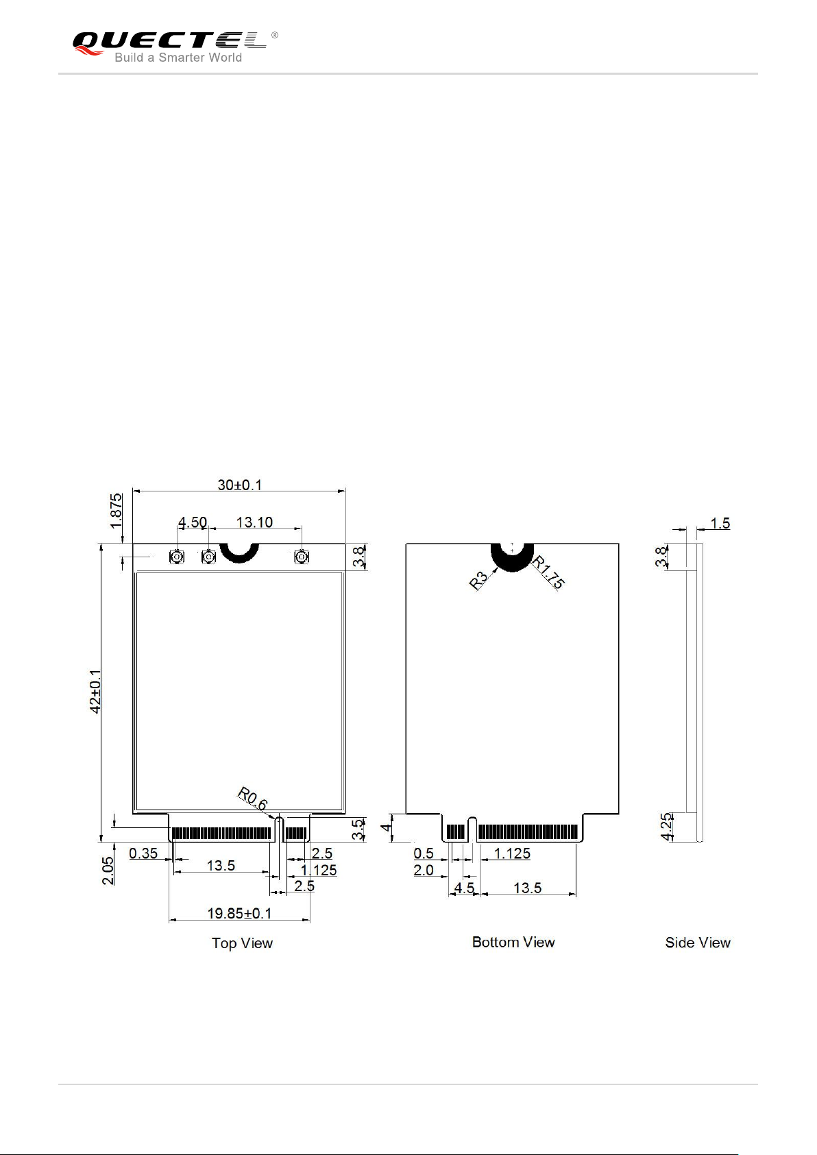
LTE-A Module Series
EM12-G Hardware Design
7 Mechanical Dimensions and
Packaging
This chapter mainly describes mechanical dimensions and packaging specifications of EM12-G module.
All dimensions are measured in mm, and the tolerances for dimensions without tolerance values are
±0.05mm.
7.1. Mechanical Dimensions of the Module
Figure 29: Mechanical Dimensions of EM12-G (Unit: mm)
EM12-G_Hardware_Design 56 / 62

LTE-A Module Series
EM12-G Hardware Design
7.2. Standard Dimensions of M.2 PCI Express
The following figure shows the standard dimensions of M.2 PCI Express. Please refer to document [4]
for detailed A and B.
Figure 30: Standard Dimensions of M.2 Type 3042-S3 (Unit: mm)
According to M.2 nomenclature, EM12-G is Type 3042-S3-B (30.0mm × 42.0mm, max component height
on the top is 1.5mm and single-sided, key ID is B).
Figure 31: M.2 Nomenclature
EM12-G_Hardware_Design 57 / 62

LTE-A Module Series
These are design effect drawings of EM12-G module. For more accurate pictures, please refer to the
module that you get from Quectel.
NOTE
EM12-G Hardware Design
7.3. Design Effect Drawings of the Module
Figure 32: Top View of the Module
7.4. M.2 Connector
EM12-G adopts a standard PCI Express M.2 connector which compiles with the directives and standards
listed in the document [4].
7.5. Barcode Rule
The PN (Q1-A2449) printed on the label is fixed for Quectel.
For the SN shown in the top view, the first two digits indicate project stage. For example, “D1” means
DVT1. The next one digit indicates the code of the factory where the module is manufactured. The next
EM12-G_Hardware_Design 58 / 62

LTE-A Module Series
EM12-G Hardware Design
four digits indicate the day, month and year when the module is manufactured. For instance, “18FD”
means 13th June, 2018. The next two digits indicate serial number of the manufacturing order. The last six
digits vary by module which could not be the same in certain time. Meanwhile, the SN and IMEI can be
checked by scanning the QR code.
7.6. Packaging
EM12-G modules are packaged in trays. The following figure shows the tray size.
Figure 33: Tray Size
Each tray contains 10 modules. The smallest package contains 100 modules. Tray packaging procedure
as below.
1. Use 10 trays to package 100 modules at a time (tray size: 247mm × 172mm).
2. Place an empty tray on the top of the 10-tray stack.
3. Fix the stack with masking tape in “#” shape as shown in the figure.
4. Pack the stack with conductive bag, and then fix the bag with masking tape.
5. Place the IMEI No. list into the small carton.
6. Seal the carton and then label the seal with sealing sticker (small carton size: 250mm × 175mm ×
128mm).
EM12-G_Hardware_Design 59 / 62

LTE-A Module Series
EM12-G Hardware Design
Figure 34: Tray Packaging Procedure
EM12-G_Hardware_Design 60 / 62

LTE-A Module Series
SN
Document Name
Remark
[1]
Quectel_M.2_EVB_User_Guide
M.2 EVB User Guide
[2]
Quectel_EP06&EG06&EM06_AT_Commands_Manual
EP06, EG06 and EM06 AT
Commands Manual
[3]
Quectel_EP06&EG06&EM06_GNSS_AT_Commands_
Manual
EP06, EG06 and EM06 GNSS AT
Commands Manual
[4]
PCI Express M.2 Specification
PCI Express Specification
Abbreviation
Description
bps
Bits Per Second
DC-HSPA+
Dual-carrier High Speed Packet Access
DFOTA
Delta Firmware Upgrade Over The Air
DL
Down Link
ESD
Electrostatic Discharge
FDD
Frequency Division Duplexing
GLONASS
GLObalnaya Navigatsionnaya Sputnikovaya Sistema, the Russian Global
Navigation Satellite System
GNSS
Global Navigation Satellite System
GPS
Global Positioning System
GSM
Global System for Mobile Communications
HR
Half Rate
HSPA
High Speed Packet Access
EM12-G Hardware Design
8 Appendix References
Table 30: Related Documents
Table 31: Terms and Abbreviations
EM12-G_Hardware_Design 61 / 62

LTE-A Module Series
HSUPA
High Speed Uplink Packet Access
kbps
Kilo Bits Per Second
LED
Light Emitting Diode
LTE
Long Term Evolution
Mbps
Million Bits Per Second
ME
Mobile Equipment (Module)
MIMO
Multiple-Input Multiple-Output
MLCC
Multiplayer Ceramic Chip Capacitor
MMS
Multimedia Messaging Service
MO
Mobile Originated
MT
Mobile Terminated
PDU
Protocol Data Unit
PPP
Point-to-Point Protocol
RF
Radio Frequency
Rx
Receive
SAR
Specific Absorption Rate
SMS
Short Message Service
Tx
Transmit
UART
Universal Asynchronous Receiver & Transmitter
UL
Up Link
URC
Unsolicited Result Code
(U)SIM
(Universal) Subscriber Identification Module
WCDMA
Wideband Code Division Multiple Access
EM12-G Hardware Design
EM12-G_Hardware_Design 62 / 62
 Loading...