

M50Hardware Design
M50
Quectel Cellul ar Engine
Hardware Design
M50_HD_V2.0
M50_HD_V2.0 - 1 -

M50Hardware Design
Quecctel
Confidential
Document Title M50 Hardware Design
Revision 2.0
Date 2012-06-26
Status Released
Document Control ID M50_HD_V2.0
General Notes
Quectel offers this information as a service to its customers, to support application and
engineering efforts that use the products de signed by Quectel. The information provid ed is
based upon requirements specifically provided for customers of Quectel. Quectel has not
undertaken any independent search for additional information, relevant to any information
that may be in the customer’s possession. Furthermore, system validation of this product
designed by Quectel within a larger electronic system remains the responsibility of the
customer or t he custome r’s syste m inte gra tor. All speci ficati ons suppl ie d her ein a re subjec t to
change.
Copyright
This d ocument contains propri etary te chnical inf ormation of Quecte l Co., Ltd. Copying this
document, distribution to others, a nd communica tion of the contents there of, are forbidden
without permission. Offenders are liable to the payment of damages. All rights are reserved in
the event of a patent grant or registration of a utility model or design. All specifications
supplied herei n are subject to change wit hout notice at any time.
Copyright © Shanghai Quectel Wireless Solutions Ltd. 2012.
M50_HD_V2.0 - 2 -

M50Hardware Design
Quecctel
Confidential
Contents
Contents ................................................................................................................................................... 3
Table Index .............................................................................................................................................. 5
Figure Index ............................................................................................................................................ 6
0. Revi s io n hi stor y .................................................................................................................................. 8
1. Introduction ....................................................................................................................................... 9
1.1. Related documents.................................................................................................................... 9
1.2. Terms and ab brevi ations ......................................................................................................... 10
1.3. Safety cautions ........................................................................................................................ 12
2. Product concept ............................................................................................................................. 15
2.1. Key fe at u re s ............................................................................................................................ 15
2.2. Functional diagram ................................................................................................................. 17
2.3. Evaluation board ..................................................................................................................... 18
3. Application interface ...................................................................................................................... 19
3.1. Pin of module .......................................................................................................................... 20
3.1.1. Pin assignment .............................................................................................................. 20
3.1.2. Pin description .............................................................................................................. 22
3.2. O pe r ating mo de s ..................................................................................................................... 29
3.3. Power supply........................................................................................................................... 30
3.3.1. Pow e r features of module ............................................................................................ 30
3.3.2. Decrease supply voltage drop ...................................................................................... 30
3.3.3. Reference design for power supply ............................................................................. 31
3.3.4. Monitor power supply .................................................................................................. 32
3.4. Power on and down scena rios ................................................................................................ 32
3.4.1. Pow e r on ....................................................................................................................... 32
3.4.2. Pow e r dow n .................................................................................................................. 34
3.4.3. Restart ........................................................................................................................... 36
3.5. Charge interface ...................................................................................................................... 38
3.6. Power saving ........................................................................................................................... 38
3.6.1. Minimum functionality mode ...................................................................................... 38
3.6.2. SLEEP mode................................................................................................................. 39
3.6.3. Wake up module f ro m S LEE P mode .......................................................................... 39
.7. Summary of state transition ................................................................................................... 39
3
3.8. RTC backup............................................................................................................................. 40
3.9. Serial in terfaces ...................................................................................................................... 41
3.9.1. UART Port .................................................................................................................... 42
3.9.2. Debug Port .................................................................................................................... 46
3.9.3. Auxiliary UART Port ................................................................................................... 46
3.9.4. UART application ........................................................................................................ 47
3.10. Audio interfaces .................................................................................................................... 50
3.10. 1. De c rease TD D noise and ot her noise ........................................................................ 51
3.10.2. Microphone interfaces design.................................................................................... 51
M50_HD_V2.0 - 3 -

M50Hardware Design
Quecctel
Confidential
3.10. 3. Receiver and s peaker int erface de sign ...................................................................... 52
3.10.4. Earphone interface design.......................................................................................... 54
3.10. 5. L ou d speake r interf ace de sign ................................................................................... 54
3.10. 6. Audio ch a r a cteristics .................................................................................................. 55
3.11. SIM card interface ................................................................................................................ 55
3.11.1. S I M car d a ppl icati o n .................................................................................................. 55
3.11. 2. 6 Pin SIM cassette ...................................................................................................... 57
3.11. 3. 8 Pi n SIM c asse tt e ...................................................................................................... 58
3.12. SD card interface .................................................................................................................. 60
3.13. PCM interface ....................................................................................................................... 62
3.13. 1. C on figuration .............................................................................................................. 62
3.13.2. Timing ......................................................................................................................... 63
3.13. 3. Refere n ce de sign ........................................................................................................ 64
3.13. 4. AT co m ma n d .............................................................................................................. 64
3.14. ADC ....................................................................................................................................... 66
3.15. Behaviors of the RI............................................................................................................... 66
3.16. Network status indication..................................................................................................... 69
3.17. Operating status indication .................................................................................................. 69
4. Antenna interface........................................................................................................................... 71
4.1. RF reference design ................................................................................................................ 71
4.2. RF output power ..................................................................................................................... 72
4.3. RF receiving sensitivity.......................................................................................................... 72
4.4. O pe r ating fre quencie s............................................................................................................. 72
4.5. RF cable soldering .................................................................................................................. 73
5. Electrical, reliability and radio characteristics ......................................................................... 74
5.1. Absolute maximum ratings .................................................................................................... 74
5.2. Operating temperature ............................................................................................................ 74
5.3. Power supply ratings .............................................................................................................. 75
5.4. Current consumption .............................................................................................................. 76
5.5. Electro-static discharge .......................................................................................................... 78
6. Mechanical dimensions ................................................................................................................ 79
.1. Mechanical dimensions of module ........................................................................................ 79
6
6.2. Re c o mmende d f ootprint with o ut bottom centre p a ds .......................................................... 81
6.4. Top view of the module ......................................................................................................... 82
6.5. Bottom view of the module.................................................................................................... 83
7. Storage and manufacturing ......................................................................................................... 84
7.1. Storage ..................................................................................................................................... 84
7.2. Soldering ................................................................................................................................. 85
7.3. Packaging ................................................................................................................................ 86
Appendix A: GPRS coding schemes ............................................................................................. 87
Appendix B: GPRS multi-slot classes............................................................................................ 88
M50_HD_V2.0 - 4 -

M50Hardware Design
Quecctel
Confidential
Table Index
TABLE 1: RELATED DOCUMENTS ..................................................................................................... 9
TABLE 2: TERMS AND ABBREVIATIONS........................................................................................ 10
TABLE 3: MODULE KEY FEATURES ................................................................................................ 15
TABLE 4: CODING SCHEMES AND MAXIMUM NET DATA RATES OVER AIR INTERFACE .. 17
TABLE 5: M50 PIN ASSIGNMENT ..................................................................................................... 21
TABLE 6: PIN DESCRIPTION ............................................................................................................. 22
TABLE 7: OVERVIEW OF OPERATING MODES.............................................................................. 29
TABLE 8: PIN DEFINITION OF THE CHARGING ............................................................................ 38
TABLE 9: SUMMARY OF STATE TRANSITION ............................................................................... 39
TABLE 10: LOGIC LEVELS OF THE UART INTERFACES.............................................................. 42
TABLE 11: PIN DEFINITION OF THE UART IN TERFACES ............................................................ 42
TABLE 12: PIN DEFINITION OF AUDIO INTERFACES .................................................................. 50
TABLE 13: AOUT3 OUTPUT CHARACTERISTICS .......................................................................... 51
TABLE 14: TYPICAL ELECTRET MICROPHONE CHARACTERISTICS ....................................... 55
TABLE 15: TYPICAL SPEAKER CHARACTERISTICS .................................................................... 55
TABLE 16: PIN DEFINITION OF THE SIM INTERFACE ................................................................. 56
TABLE 17: PIN DESCRIPTION OF AMPHENOL SIM CARD HOLDER ......................................... 58
TABLE 18: PIN DESCRIPTION OF MOLEX SIM CARD HOLDER ................................................. 59
TABLE 19: PIN DEFINITION OF THE SD CARD INTERFACE ....................................................... 60
TABLE 20: PIN NAME OF THE SD CARD AND MICRO SD CARD ............................................... 61
TABLE 21: PIN DEFINITION OF PCM INTERFACE......................................................................... 62
TABLE 22: CONFIGURATION ............................................................................................................ 62
TABLE 23: QPCMON COMMAND DESCRIPTION .......................................................................... 65
TABLE 24: QPCMVOL COMMAND DESCRIPTION ........................................................................ 65
TABLE 25: PIN DEFINITION OF THE ADC....................................................................................... 66
TABLE 26: CHARACTERISTICS OF THE ADC ................................................................................ 66
TABLE 27: BEHAVIORS OF THE RI .................................................................................................. 66
TABLE 28: WORKING STATE OF THE NETLIGHT ......................................................................... 69
TABLE 29: PIN DEFINITION OF THE STATUS................................................................................. 69
TABLE 30: PIN DEFINITION OF THE RF_ANT ................................................................................ 71
TABLE 31: THE MODULE CONDUCTED RF OUTPUT POWER .................................................... 72
TABLE 32: THE MODULE CONDUCTED RF RECEIVING SENSITIVITY .................................... 72
TABLE 33: THE MODULE OPERATING FREQUENCIES ................................................................ 72
TABLE 34: ABSOLUTE MAXIMUM RATINGS................................................................................. 74
TABLE 35: OPERATING TEMPERATURE ......................................................................................... 74
TABLE 36: THE MODULE POWER SUPPLY RATINGS ................................................................... 75
TABLE 37: THE MODULE CURRENT CONSUMPTION .................................................................. 76
TABLE 38: THE ESD ENDURANCE (TEMPERATURE:25℃,HUMIDITY:45 %)............................ 78
TABLE 39: DESCRIPTION OF DIFFERENT CODING SCHEMES .................................................. 87
TABLE 40: GPRS MULTI-SLOT CLASSES ........................................................................................ 88
M50_HD_V2.0 - 5 -

M50Hardware Design
Quecctel
Confidential
Figure Index
FIGURE 1: MODULE FUNCTIONAL DIAGRAM ............................................................................. 18
FIGURE 2: PIN ASSIGNMENT ............................................................................................................ 20
FIGURE 3: VOLTAGE RIPPLE DURING TRANSMITTING ............................................................. 30
FIGURE 4: REFERENCE CIRCUIT FOR THE VBAT INPUT ............................................................ 31
FIGURE 5: REFERENCE CIRCUIT FOR POWER SUPPLY .............................................................. 31
FIGURE 6: TURN ON THE MODULE USING DRIVING CIRCUIT................................................. 32
FIGURE 7: TURN ON THE MODULE USIN G KE Y STROKE ........................................................... 33
FIGURE 8: TIMING OF TURNING ON SYSTEM .............................................................................. 33
FIGURE 9: TIMING OF TURNING OFF THE MODULE................................................................... 34
FIGURE 10: REFERENCE CIRCUIT FOR EMERG_OFF BY USING DRIVING CIRCUIT ............ 36
FIGURE 11: REFERENCE CIRCUIT FOR EMERG_OFF BY USING BUTTON .............................. 36
FIGURE 12: TIMING OF RESTARTING SYSTEM ............................................................................ 37
FIGURE 13: TIMING OF RESTAR TING SYSTEM AFTER EMERGENCY SHUTDOWN .............. 37
FIGURE 14: RTC SUPPLY FROM NON-CHARGEABLE BATTERY ............................................... 40
FIGURE 15: RTC SUPPLY FROM RECHARGEABLE BATTERY .................................................... 40
FIGURE 16: RTC SUPPLY FROM CAPACITOR ................................................................................ 40
FIGURE 17: SEIKO XH414H-IV01E CHARGE CHARACTERISTICS ............................................. 41
FIGURE 18: REFERENCE DESIGN FOR FULL-FUNCTION UART ................................................ 44
FIGURE 19: REFERENCE DESIGN FOR UART PORT ..................................................................... 44
FIGURE 20: REFERENCE DESIGN FOR UART PORT WITH HARDWARE FLOW CONTROL... 45
FIGURE 21: REFERENCE DESIGN FOR FIRMWARE UPGRADE .................................................. 45
FIGURE 22: REFERENCE DESIGN FOR DEBUG PORT .................................................................. 46
FIGURE 23: REFERENCE DESIG N FOR AUXILIAR Y UART PORT ............................................... 47
FIGURE 24: LEVEL MATCH DESIGN FOR 3.3V SYSTEM.............................................................. 47
FIGURE 25: LEVEL MATCH DESIGN FOR 5V SYSTEM................................................................. 48
FIGURE 26: LEVEL MATCH DESIGN FOR RS-232 .......................................................................... 49
FIGURE 27: REFERENCE DESIG N FOR AIN1&AIN2...................................................................... 52
FIGURE 28: REFERENCE DESIG N FOR AOUT1 .............................................................................. 52
FIGURE 29: HANDSET INTERFACE DESIGN FOR AOUT2 ........................................................... 53
FIGURE 30: SPEAKER INTERF A CE DESIGN WITH AN AMPLIFIER F OR AOUT2 ..................... 53
FIGURE 31: EARPHONE INTERFACE DESIGN ............................................................................... 54
FIGURE 32: LOUD SPEAKER INTERFACE DESIGN ....................................................................... 54
FIGURE 33: REFERENCE CIRCUIT OF THE 8 PINS SIM CARD .................................................... 56
FIGURE 34: REFERENCE CIRCUIT OF THE 6 PINS SIM CARD .................................................... 57
FIGURE 35: AMPHENOL C707 10M006 512 2 SIM CARD HOLDER .............................................. 58
FIGURE 36: MOLEX 91228 SIM CARD HOLDER ............................................................................ 59
FIGURE 37: REFERENCE CIRCUIT OF SD CARD ........................................................................... 60
FIGURE 38: LONG SYNCHRONIZATION & SIGN EXTENSION DIAGRAM ............................... 63
FIGURE 39: LONG SYNCHRONIZATION & ZERO PADDING DIAGRAM ................................... 63
FIGURE 40: SHORT SYNCHRONIZATION & SIGN EXTENSION DIAGRAM .............................. 63
FIGURE 41: SHORT SYNCHRONIZATION & ZERO PADDING DIAGRAM ................................. 64
M50_HD_V2.0 - 6 -

M50Hardware Design
Quecctel
Confidential
FIGURE 42: REFERENCE DESIGN FOR PCM .................................................................................. 64
FIGURE 43: RI BEHAVIOR OF VOICE CALLING A S A RECEIVER .............................................. 67
FIGURE 44: RI BEHAVIOR OF DATA CALLING AS A RECEIVER ................................................ 67
FIGURE 45: RI BEHAVIOR AS A CALLER ........................................................................................ 67
FIGURE 46: RI BEHAVIOR OF URC OR SMS RECEIVED .............................................................. 68
FIGURE 47: REFERENCE DESIGN FOR NETLIGHT ....................................................................... 69
FIGURE 48: REFERENCE DESIGN FOR STATUS ............................................................................ 70
FIGURE 49: REFERENCE DESIGN FOR RF ...................................................................................... 71
FIGURE 50: RF SOLDERING SAMPLE.............................................................................................. 73
FIGURE 51: M50 TOP A ND SIDE DIMENSIONS .............................................................................. 79
FIGURE 52: M50 BOTTOM DIMENSIONS ........................................................................................ 80
FIGURE 53: RECOMMENDED FOOTPRINT WITHOUT BOTTOM CENTRE PADS .................... 81
FIGURE 55: TOP VIEW OF THE MODULE ....................................................................................... 82
FIGURE 56: BOTTOM VIEW OF THE MODULE .............................................................................. 83
FIGURE 57: PASTE A PPLICATION .................................................................................................... 85
FIGURE 58: RAMP-SOAK-SPIKE REFLOW PROFILE .................................................................... 86
FIGURE 59: MODULE TRAY .............................................................................................................. 86
FIGURE 60: RADIO BLOCK STRUCTURE OF CS-1, CS-2 AND CS-3 ........................................... 87
FIGURE 61: RADIO BLOCK STRUCTURE OF CS-4 ........................................................................ 87
M50_HD_V2.0 - 7 -
M50Hardware Design
Quecctel
Confidential
0. Revision history
Revision Date Author Description of change
1.0 2011-12-20 Ray XU Initial
1.1 2012-02-03 Ray XU 1. Updated PCM interface
2. Updated SD interface
3. Updated charging interface
4. Updated timing of turn ing on the module
1.2 2012-07-20 Bal y BAO 1. Deleted the USB interface
2. Deleted the camera interface
1.3 2012-10-22 Mountain Z H OU 1. Updated functional diagram
2. Update d re fe rence des ign cir c uit
3. Update d a udio char a cteris tics
4. Updated VRTC DC characteristics
5. Updated SLEEP current consumption
6. Update d i nternet se r vice protocol s
7. Updated SIM pins’ name
8. Modified PCM function
9. Deleted F AX function
2.0 2012-06-16 Ray XU 1. Update the m odule si ze
2. Update the pin layout
M50_HD_V2.0 - 8 -
M50 Hardware Design
Draft new
Digital cellular telecommunications (Phase 2+); AT
Data Circuit
DCE) interface for
Short Message Service (SMS) and Cell Broadcast
hase 2+);
Digital cellular telecommunications (Phase 2+);
Digital cellular telecommunications (Phase 2+);
Quecctel
Confidential
1. Introduction
This do cument defines the M50 module and describes the hardware interface of M50 which are
connected with the customer application and the air interface.
This do cument can help customers quickl y unders tan d module interface specifications, electrical
and mechanical details. Associated with application notes and user guide, customers can use
M50module to design and set up mobile applications easily.
1.1. Related document s
Table 1: Related documents
SN Document name Remark
[1] M50_ ATC AT commands set
[2] ITU-T
rec omme nda ti on V.25t er
[3] GSM 07.07
[4] GSM 07.10 Supp ort GSM 07 .1 0 multipl exing proto co l
[5] GSM 07.05 Digital cellular telecommunications (Phase 2+); Use
[6] GSM 11.1 4 Digital cellular telecommunications (P
[7] GSM 11.11
[8] GSM 03.38
[9] GSM 11.10 Digital cellular teleco mmuni cations (P h ase 2); Mobile
[10] GSM_UART_AN UART port application note
[11] GSM_FW_Upgrade_AN01 GSM Firm w a re upgrade appl icatio n not e
[12] M10_EVB_UGD
Serial asynchronous automatic dialing and control
command set for GSM Mobile Equipment (ME)
of Data Terminal Equipment –
terminating Equipment (DTE –
Service (CBS)
Specification of the SIM Application Toolkit for the
Subscriber Identity module – Mobile Equipment (SIM
– ME) interfa ce
Specification of the Subscriber Identity module –
Mobile Equipment (SIM – ME) interface
Alphabets and language-specific information
Station (MS) conformance specification; Part 1:
Conformance specificat ion
M10 EVB user gui d
e
M50_HD_V2.0 - 9 -
M50 Hardware Design
Quecctel
Confidential
1.2. T erm s and abbreviations
Table 2: Te rms and abb reviati o ns
Abbreviation Description
ADC Analog-to-Digital Converter
AMR Adaptive Multi-Rate
ARP Antenna Reference Point
ASIC Application Specific Integrated Circuit
BER Bit Error Rate
BOM Bill Of Material
BTS Base Transceiver Station
CHAP Challenge Handshake Authentication Protocol
CS Coding Scheme
CSD Circuit Switched Data
CTS Clear To Send
DAC Digital-to-An alo g Co nverter
DRX Discontinuous Reception
DSP Digital Signal Processor
DCE Data Communications Equipment (typically module)
DTE Data Terminal Equipment (typically computer, external co ntroller)
DTR Data Terminal Ready
DTX Discontinuous Transmission
EFR Enhanced Full Rate
EGSM Enha nced GSM
EMC Electromagnetic Comp atibilit y
ESD Electrostatic Discharge
ETS European Telecomm unica tion Sta nda rd
FCC Federal Communications Commission (U.S.)
FDMA Frequency Division Multiple Access
FR Full R ate
GMSK Gaussian Minimum Shift Keying
GPRS G enera l Packet Radio Service
GSM Global System for Mobile Communications
HR Half R at e
I/O Input/Output
IC Integrate d Circuit
IMEI International Mobile Equipment Identity
Imax Maximum Load Current
Inorm Normal Current
kbps Kilo Bits Per Second
LED Light Emitting Diode
M50_HD_V2.0 - 10 -
M50 Hardware Design
Quecctel
Confidential
Li-Ion Lithium-Ion
MO Mobile Ori ginated
MS Mobile Station (GSM engine)
MT Mobile Terminated
PAP Password Authentication Protocol
PBCCH Packet Switched Broadcast Control Channel
PCB Printe d Circuit B oard
PDU Protocol Data Unit
PPP Point-to-Point Protocol
RF Radio Frequency
RMS Root Mean Square (value)
RTC Real Time Clock
RX Receive Direction
SIM Subscriber Identification Module
SMS Short Message Service
TDMA Time Division Multiple Access
TE Terminal Equipment
TX Transmitting Direction
UART Unive rs al Asyn c hr o no us Receiver & Transmitter
URC Unsolicited Result Code
USSD Unstructured Supplementary Service Data
VSWR Voltage Standing Wave Ratio
Vmax Maximum Voltage Value
Vnorm Normal Voltage Value
Vmin Minimum Voltage Value
VIHmax Maximum Input High Level Voltage Value
VIHmin Minimum Input High Level Voltage Value
VILmax Maximum Input Low Level Voltage Value
VILmin Minimum Input Low Level Voltage Value
VImax Absolute Maximum Input Voltage Value
VImin Absolute Minimum Input Voltage Value
VOHmax Maximum Output Hi gh Level Voltage Value
VOHmin Minimum Outp ut High Leve l Volta ge V al ue
VOLmax M ax i m u m Ou tput Low Leve l Volta ge V al ue
VOLmin Minim um Outp ut L ow Level Vol t a ge Value
Phonebook abbreviations
LD SIM Last Dialing phoneb oo k (l ist of num bers m ost recent ly dialed)
MC Mobile Equipment list of unanswered MT Calls (missed calls)
ON SIM (or ME) Own Numbers (MSISDNs) list
RC Mob ile Equipment list of Received Calls
SM SIM phonebook
M50_HD_V2.0 - 11 -
M50 Hardware Design
station, fuel
safety haza r d.
Quecctel
Confidential
1.3. Safety cautions
The following safety precauti ons must be observed during all phases of the operation, such as
usage, service or repair of any cellular terminal or mobile incorporating M50module.
Manufacturers of t he cell ula r termi nal sho uld se nd the follo wing sa fety i nform ation t o use rs and
operating personnel and to incorpo rat e the se gui de li nes int o al l manual s supplied with the pr o du ct.
If not so, Quectel does not take on any liability for customer failure to comply with these
precautions.
When i n a hos pit al or ot her healt h c are f acili ty, obse rve the rest ricti ons about the
use of mo bi l e. Switch the cellular terminal or mobile off. Medical equipment may
be sensitive to not operate n o rm ally for RF energy interference.
Switch off the cell ul ar te rmin al or mobi le bef ore boa rdin g an air craft . Make sure
it switched off. The ope ratio n o f wirel ess appli a n ces i n an ai r c raft is f or bidde n to
preve nt inte rfere nce wit h commu nic atio n syst e ms. Forget to think much of these
inst ruct ions ma y l ead to the flight safety or offend against local legal action, or
both.
Do not ope r ate t he cell ul ar te rmi nal or mobil e i n t he pre se nce o f fl amm able gas
or fume. Switch off the cellul ar t ermin al when you a re near pet rol
depot, chemical plant o r where bl astin g operat ions are i n progre ss. Ope ratio n of
any electrical equipment in potentially explosive atmosphere can constitute a
Your cellular terminal or mobile receives and transmits radio frequency energy
while swi t ched o n. RF i nte rfe re n ce can oc cur i f i t is use d clo se t o TV set, radio,
comput er or other electric equipment.
Road s afe ty co mes first! Do no t us e a hand-held cellular terminal or mobile while
driving a vehicle, unless it is securely mounted in a holder for hands-free
operation. Before making a call with a hand-held terminal or mobile, park the
vehicle.
M50_HD_V2.0 - 12 -
M50 Hardware Design
Quecctel
Confidential
GSM cellular terminals or mobiles operate over radio frequency signal and
According to the R&TTE Directive 1999/95/CE, all wireless equipment and
telecommuni cations terminals sold in EU must meet all the stipulated he alth,
safety RF, EMC requirements th at pro vi de fo r CE m ar k. Que cte l M odul e M50
is fully in ac co r da n ce with all the di rective s of EU.
cellular network and cannot be guaranteed to connect in all conditions, for
exam ple no mobil e fee o r an inv ali d SI M card. Whi le you are in t his condition
and need emergent help, Please Remember using emergency call. In order to
make or receive call, the cellul ar termina l or mobile must be swit che d on and in
a servi ce area with a d e quat e cel lular sign al strength.
Some net works d o not allo w for e merge ncy c all if certai n net work se rvice s or
phone feat ures are in use ( e .g. lock fu n cti o ns, fixed diali n g et c . ) . You m a y have
to deactivate t h ose features bef ore you c an ma ke an eme r ge n c y c all .
Also, some networks require that a valid SIM card be properly inserted in
cellular terminal or mobile.
1.4. Directives and standard s
The M50 module is designed to comply with the FCC statements. FCC ID: XMR201211M50.
The Host system using M50, should have label indicated contains FCC ID: XMR201211M50.
1.4.1. FCC Statemen t
1. This devi ce complies with Part 15 o f the FCC rules. Oper ation is subje ct to the following
conditions:
a) Thi s device ma y not c aus e harmful interference.
b) This device must accept any interference received, including interference that may cause
undesired operation.
2. Changes or modi fications not expressl y approved by the party responsible for compliance
coul d void the user ’s authority to operate the equipment.
1.4.2. FCC Radiation exposure statement
This equipment complies with FCC radiation exposure limits set forth for an uncontrolled
environment. This equipment should be installed and operated with minimum distance 20cm
between the radiator and your body as well as kept minimum 20cm from radio antenna depending
on the Mobile status of this module usage.
M50_HD_V2.0 - 13 -
M50 Hardware Design
Quecctel
Confidential
The m a nu al of t he host syste m, whi ch uses M50, must include RF exposure warning statement to
advi ce use r shoul d keep mi nim um 20c m fr om the r adi o ante n n a o f M 50 m od ul e depe nding on the
Mobile status.
The following list of antenna is indicating the maximum permissible antenna gain.
Type Maxim u m Gain
(850Hz/900Hz)
External
Antenna
Internal
Antenna
This radio module must not be installed to co-locate and operate simu
ltaneously with other radios in host system;
additional testing and equipment authorization may be required to op
erating simultaneously with other radios.
Monopole 0.5dBi 2dBi 50Ω
Vehicular antenna 0.5dBi 2dBi 50Ω
Monopole 0.5dBi 2dBi 50Ω
PIFA 0.5dBi 2dBi 50Ω
FPC 0.5dBi 2dBi 50Ω
PCB 0.5dBi 2dBi 50Ω
Maxim u m Gain
(1800Hz/1900Hz)
Impedance
M50_HD_V2.0 - 14 -
M50 Hardware Design
Quecctel
Confidential
2. Product concept
M50 is a Quad-band GSM/GPRS engine that works at frequencies of GSM850MHz,
GSM900MHz, DCS1800MHz and PCS1900MHz. The M50 features GPRS multi-slot class 12
and supports the GPRS coding schemes CS-1, CS-2, CS-3 and CS-4. For more details about
GPRS multi-slot cl as s es a nd co ding sche me s, plea se re fer to the Appendix A an d Appendix B.
With a tin y profile of 24.5mm×25.3mm
for M2M applications, including Vehicles and Personal Tracking, Se c urity S yst em, Wireless POS,
Industrial PDA, Smart Metering, and Remote Maintenance & Control etc.
M50 is an SMD type module with LCC package, which can be embedded in customer’s
applications. It provides abundant hardware inter faces bet ween the module and customer’s hos t
board.
Designed with power s avin g techni que , t he curre nt consumpti on of M50 is as l ow as 1.3 mA i n
SLEEP mode when DRX is 5.
M50 is integra te d with Internet service protocols, su c h as TCP, UD P , F TP and P PP . Exten ded AT
commands h ave been developed for customer to use these Internet service protocols easily.
The module fully complies with the RoHS directive of the European Union.
×2.6mm, the module can meet almost all the requirements
2.1. Key features
Table 3: Module key features
Feature Description
Power supply Single supply voltage 3.3V~ 4.6V
Typical supply voltage 4.0V
Pow er saving Typical p o we r consumpt i on i n SLEEP mode: 1.3 mA@ DRX=5
1.2 mA@ DRX=9
Frequency bands Quad-band: GSM850, GSM900, DCS1800, PCS1900.
The module can se arch these frequency bands automatically
The frequency bands can be set by AT command.
Compliant with GSM Phase 2/2+
GSM class Small MS
Trans mi tt ing po wer Class 4 ( 2W) at GSM850 and GSM900
Cla ss 1 ( 1W) at DCS1800 and PCS1900
GPRS connectivity GPRS multi-sl o t clas s 12 (default)
GPRS multi-slot clas s 1~12 (configurable)
GPRS mobile station class B
M50_HD_V2.0 - 15 -
M50 Hardware Design
Quecctel
Confidential
Te mp er at ure rang e Nor m al o pe r ation: -35°C ~ +80°C
Restricted operation: -40°C ~ -35° C and +80°C ~ +85°C
Storage temperature: -45°C ~ +90°C
DATA GPRS:
CSD:
SMS Text and PDU mode
SIM interface Sup port SIM c ar d: 1.8V, 3V
Audi o features Speech codec modes:
UART interfaces UART Port:
Phonebook ma nagement Support phonebook types: SM, ME, ON, M C, RC, DC, LD, LA
SIM Application Toolkit Support SAT class 3, GSM 11.14 Release 99
Real time clock Supported
Ph ys ical ch aract eri s ti cs Size:
Firmware upgrade Firmware upgrade via UART Port
GP RS data do wnl ink tra ns fer: m ax. 85. 6 kbps
GPRS d at a uplink t r an sfer: ma x. 85.6 kbps
Coding scheme: CS-1, CS-2, CS-3 and CS-4
Support the protocols PAP (Password Authentication Protocol)
usually used for PPP connections
Internet service protocols
TCP/UDP/FTP/PPP/HTTP/NTP/PING
Support Packet Broadcast Control Channel (PBCCH)
CSD tr an s mi s sion rat e s: 2. 4, 4. 8, 9. 6, 14.4 kbp s non-transparent
Support Unstructured Supplementary Service Data (USSD)
SMS storage: SIM card
Half Rate (ETS 06.20)
Full Rate (ETS 06.10)
Enhanced Full Rate (ETS 06.50 / 06.60 / 06.80)
Adaptive Multi-Rate (AMR)
Echo Suppress ion
E cho C ancel latio n
Noi se Re d u ction
Embedded one amplifier o f clas s A B with maximum driving
power up to 800mW
Seven lines on UART port interface
Used for AT command, G P R S dat a a n d CSD d ata
Multiplexing function
Sup port aut obaudi n g f ro m 4800 bps to 11520 0 bp s
Debug Port:
Two lines on debug port interface DBG_TXD and DBG_RXD
De bu g P o rt only use d fo r firmware deb ugging
Auxiliary Port:
Used for AT command
24.5 (±0.15) × 25.3 (±0.15) × 2.6 (±0.2) mm
Weight: 3.3g
1)
M50_HD_V2.0 - 16 -
M50 Hardware Design
Quecctel
Confidential
Antenna interface Connected to antenna pad with 50 Ohm impedance control
1)When the module works in this temperature range, the deviations from the GSM specification
may occur. For example, the frequency error or the phase error will be increased.
Table 4: Coding schemes and maximum net data rates over air interface
Coding scheme 1 Timeslot 2 Time slot 4 Times l ot
CS-1 9.05kbps 18.1kbps 36.2kbps
CS-2 13.4kbps 26.8kbps 53.6kbps
CS-3 15.6kbps 31.2kbps 62.4kbps
CS-4 21.4kbps 42.8kbps 85.6kbps
2.2. Fu n c ti o nal di ag r a m
The following figure shows a block diagram of the M50 module and illustrates the major
functional parts:
Power management
Baseband
Serial Flash
The radio frequency part
The peripheral interface
—Charge interface
—PCM interface
—SD interface
—SIM interface
—Audio interface
—Serial interface
—Power supply
—RF interface
—ADC
—Turn on/off interface (PWRKEY & EMERG_OFF)
M50_HD_V2.0 - 17 -
M50 Hardware Design
BB&RF
RF PAM
SAW
Filter
Serial
Flash
32KHz
26MHz
RF Transceiver
Audio
RTC
GPIO
Serial
Interface
Memory
Interface
PCM
Interface
SIM
Interface
SD
Interface
ADC
RF_ANT
VBAT
PWRKEY
EMERG_OFF
VRTC
ADC
STATUS&
NETLIGHT
UART
SIM
Interface
Audio
SD
Interface
PCM
Inteface
Reset
ESD
PMU
Charge
Interface
Charge
Quecctel
Confidential
Figure 1: Module functional diagram
2.3. Evaluatio n bo ard
In orde r t o he lp cu st o mer to deve lop a pplicat i o ns with M50 , Quectel supplies an evaluation board
(EVB) , RS -232 to USB cable , powe r adapte r, e arphone , ante nna and ot her pe riphe rals to control
or test the module. For details, please refer to the document [ 12].
M50_HD_V2.0 - 18 -

M50 Hardware Design
Quecctel
Confidential
3. Application interface
The mo dul e is equi pped w it h 83-pin SMT pads and i t ad opts LCC package. Detailed descriptions
on Sub -interfaces included in these pads are given in the following chapters:
Power supply
Power on/down
Charge interface
RTC
Serial interfaces
Audio interfaces
SIM interface
SD interface
PCM interface
ADC
M50_HD_V2.0 - 19 -
M50 Hardware Design
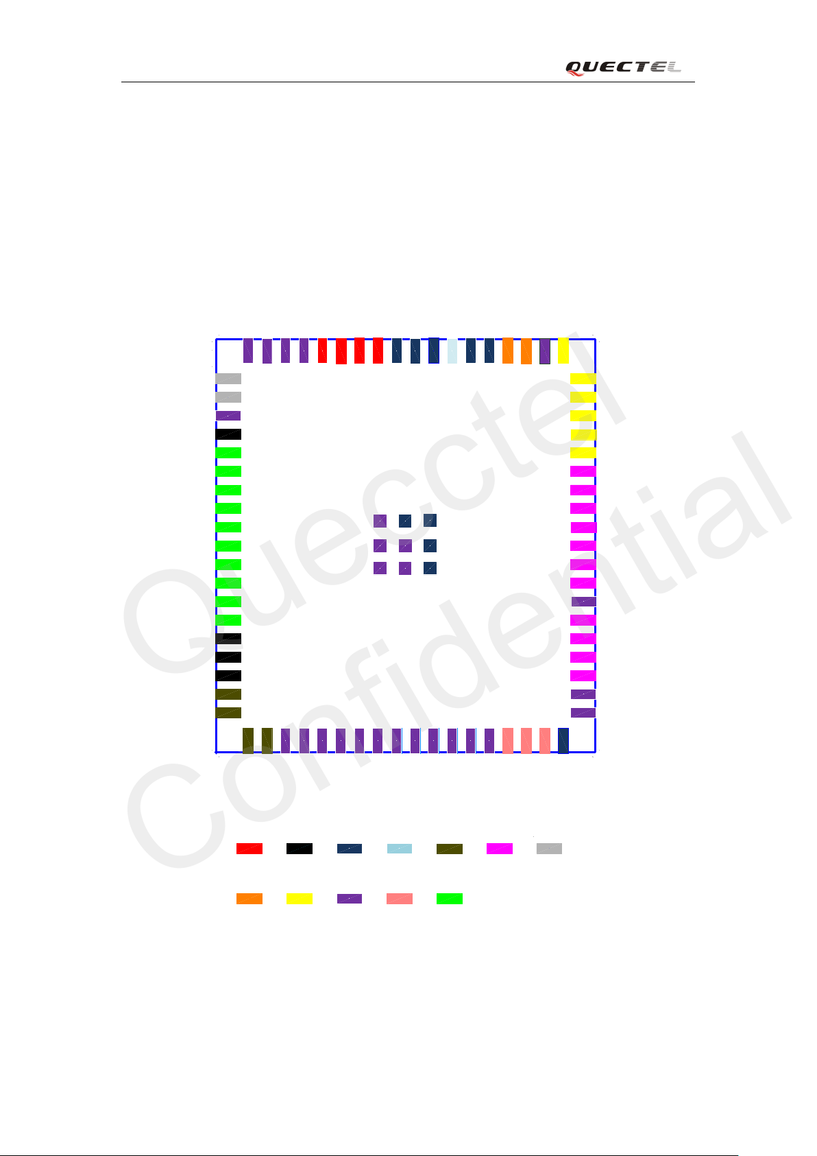
1
2
3
4
5
6
7
8
9
10
11
12
13
14
15
16
17
18
19
20 21 22 23 24 25 26 27 28 29 30 31 32 33 34 35 36 37
38
39
40
41
42
43
44
45
46
47
48
49
50
51
52
53
54
55
56
575859606162636465666768697071727374
Top view
75
76
77
78
79
80
81
82
83
SIM_PRESENCE
RESERVED
VRTC
VDD_EXT
GND
GND
RF_ANT
GND
GND
GND
VBAT
VBAT
VBAT
VBAT
RESERVED
RESERVED
RESERVED
RESERVED
ADC1
ADC0
RESERVED
NETLIGHT
SPK2P
AGND
MIC2P
MIC2N
MIC1P
MIC1N
SPK1N
SPK1P
LOUDSPKN
LOUDSPKP
STATUS
PWRKEY
EMERG_OFF
PCM_IN
PCM_CLK
RESERVED
RESERVED
TXD_AUX
RXD_AUX
DBG_TXD
DBG_RXD
RESERVED
DCD
RI
DTR
CTS
RTS
RXD
TXD
SIM1_GND
SIM1_RST
SIM1_CLK
SIM1_DATA
SIM1_VDD
VBAT GND
PCMRFUART
Power
SIM
Reserved Audio
ADC
Other
SD
PCM_OUT
PCM_SYNC
RESERVED
RESERVED
RESERVED
RESERVED
RESERVED
RESERVED
RESERVED
RESERVED
RESERVED
RESERVED
RESERVED
RESERVED
SD_CMD
SD_CLK
SD_DATA0
GND
RESERVED
RESERVED
RESERVED
RESERVED
GND
GND
GND
GND
Quecctel
Confidential
3.1. Pin of module
3.1.1. Pin assignment
Figure 2: Pin assignment
M50_HD_V2.0 - 20 -
M50 Hardware Design
管脚号
管脚名
输入/输出
管脚号
管脚名
输入/输出
Quecctel
Confidential
Table 5: M50 pin assignment
1 ADC1 I 2 ADC0 I
3 RESERVED 4 NETLIGHT O
5 SPK2P O 6 AGND
7 MIC2P I 8 MIC2N I
9 MIC1P I 10 MIC1N I
11 SPK1N O 12 SPK1P O
13 LOUDSPKN O 14 LOUDSPKP O
15 STAT US O 16 PWRKEY I
17 EMERG_OFF I 18 PCM_IN I
19 PCM_CLK O 20 PCM_OUT O
21 PCM_SYNC O 22 RESERVED
23 RESERVED 24 RESERVED
25 RESERVED 26 RESERVED
27 RESERVED 28 RESERVED
29 RESERVED 30 RESERVED
31 RESERVED 32 RESERVED
33 RESERVED 34 SD_CMD O
35 SD_CLK O 36 SD_DATA0 I/O
37 GND 38 RESERVED
39 RESERVED 40 TXD_AUX O
41 RXD_AUX I 42 DBG_TXD O
43 DBG_RXD I 44 RESERVED
45 DCD O 46 RI O
47 DTR I 48 CTS O
49 RTS I 50 RXD I
51 TXD O 52 SIM_GND
53 SIM_RST
55 SI M_ DATA I/O 56 SIM_VDD O
57 SIM_PRESENCE I 58 RESERVED
59 VRTC I/O 60 VDD_EXT O
61 GND 62 GND
63 RF_ANT I/O 64 GND
65 GND 66 GND
O 54 SIM_CLK O
67 VBAT I 68 VBAT I
69 VBAT I 70 VBAT I
71 RESERVED 72 RESERVED
M50_HD_V2.0 - 21 -
M50 Hardware Design
Quecctel
Confidential
73 RESERVED 74 RESERVED
75 RESERVED 76 RESERVED
77 RESERVED 78 RESERVED
79 GND 80 GND
81 GND 82 GND
83 GND
Note: Keep all reserved pins open.
3.1.2. Pin description
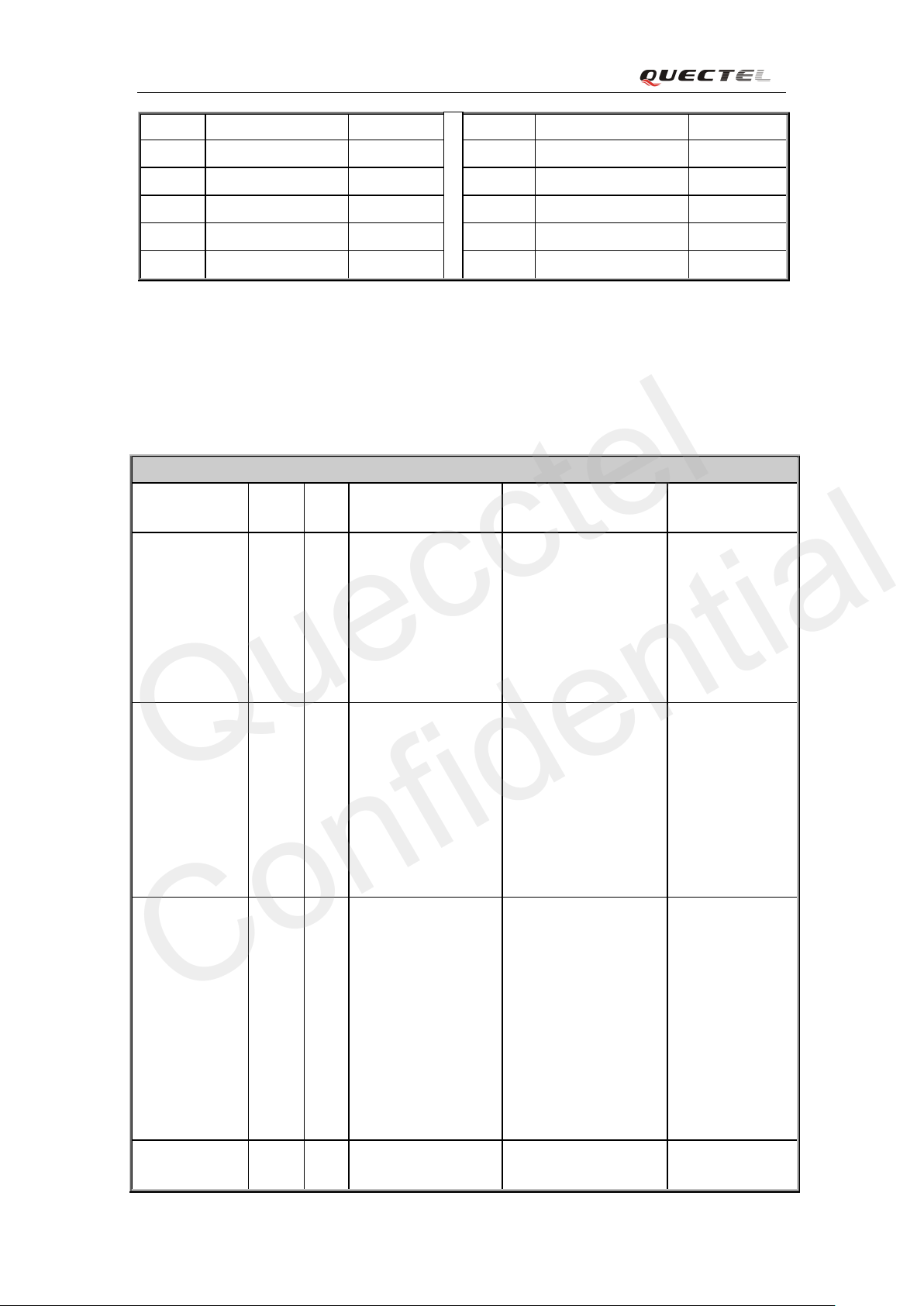
Table 6: Pin description
Power supply
PIN NAME PIN
NO.
VBAT 67,
68,
69,
70
VRTC 59 I/O Power supply for
VDD_EXT 60 O Suppl y 2.8V volt a ge
GND 37,
61,
I/O DESCRIPTION DC
CHARACTERISTICS
I Main power supply
of module:
VBAT=3.3V~4.6V
RTC when VB AT is
not supplied for the
system.
Chargi n g f or backup
battery or golden
capacitor when the
VBAT is supplied.
for external circuit.
Ground
Vm ax= 4.6V
Vmin=3.3V
Vnorm=4.0V
VImax=3.3V
VImin=1.5V
VInorm=2.8V
VOmax=2.85V
VOmin=2.6V
VOnorm=2.8V
Iout(max)= 1mA
Iin=2.6~5 uA
Vmax=2.9V
Vmin=2.7V
Vnorm=2.8V
Imax=20mA
COMMENT
Make sure that
supply sufficient
current in a
transmitting
burst which
typica lly rises to
1.6A.
If unused, keep
this pin open.
1. If unused,
keep this pin
open.
2. Re co mmended
to add a
2.2~4.7uF
bypass capacitor
when supplying
power for
ext e rnal cir cuit .
M50_HD_V2.0 - 22 -
M50 Hardware Design
Quecctel
Confidential
62,
64,
65,
66,
Tu rn on /off
PIN NAME PIN
NO.
PWRKEY 15 I Turn on/off control.
Emergency shutdown
PIN NAME PIN
NO.
EMERG_OFF 17 I Emergency off.
Module indicator
PIN NAME PIN
NO.
STAT US 16 O Indicate module
Audio in t e rface
I/O DESCRIPTION DC
CHARACTERISTICS
VILmax=
PWRKE Y sh ou l d be
pulle d down for a
moment to turn on
or off the system.
I/O DESCRIPTION DC
Pulled dow n fo r at
least 20ms , whi c h
will turn of f the
module in case of
emergency. Use it
only when normal
shutdown t hrough
PWRKEY or A T
command cannot
perform well.
I/O DESCRIPTION DC
operat in g status.
High level indicates
module is power-on
and low level
indicates
power-down.
0.1×VBAT
VIHmin=
0.6×VBAT
VI max=V BAT
CHARACTERISTICS
VILmax=0.4V
VIHmin=2.2V
V
open
CHARACTERISTICS
VOHmin=
0.85×VDD_EXT
VOLmax=
0.15×VDD_EXT
max=2.8V
COMMENT
Pulled up to
VBAT internally.
COMMENT
Open
drain/collector
driver required in
cellular device
application.
If unused, keep
this pin open.
COMMENT
If unused, keep
this pi n open.
PIN NAME PIN
MIC1P
MIC1N
M50_HD_V2.0 - 23 -
NO.
9, 10 I Channe l one for
I/O DESCRIPTION DC
CHARACTERISTICS
I f unused, keep
positive and
negative voice-band
input
COMMENT
these pins open.
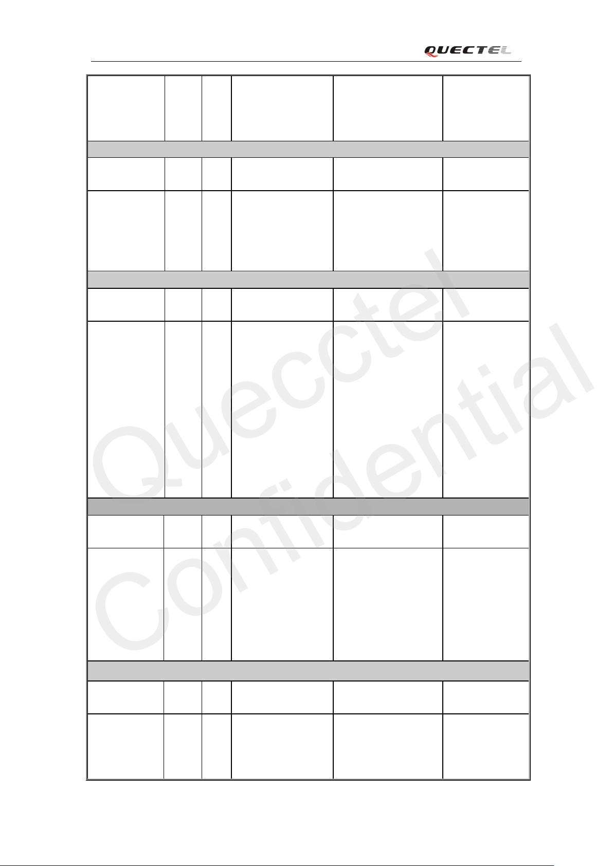
M50 Hardware Design
Quecctel
Confidential
MIC2P
MIC2N
SPK1P
SPK1N
SPK2P 5 O Channe l t wo for
AGND 6 Analo g gr o und.
LOUDSPKN
LOUDSPKP
Net status indicator
PIN NAME PIN
7, 8 I Ch a nnel two for
positive and
negative voice-band
input
12, 11 O Channe l o ne for
positive and
negative voice-band
output
voice-band output
Constitute a pse udo
diffe rent ial ch annel
with SPK2P.
13,
14
NO.
O Channel three of
positive and
negative voice-band
output
I/O DESCRIPTION DC
1. If unuse d,
keep these pins
open.
2. Support both
1. If unused,
CHARACTERISTICS
voice a n d
ringtone output.
keep these pins
open.
2. Embedded
amplifier of class
AB internally.
3. Support both
voice a n d
ringtone output.
COMMENT
NETLIGHT 4 O Netw or k status
indication
UART Port
PIN NAME PIN
NO.
DTR 47 I Data terminal ready VILmin=0V
RXD 50 I Receive data
TXD 49 O Transmit data
RTS 51 I Request to send
CTS 48 O Clear to send
RI 46 O Ring indicator
DCD 45 O Data carrier
I/O DESCRIPTION DC
detection
VOHmin=
0.85×VDD_EXT
VOLmax=
0.15×VDD_EXT
CHARACTERISTICS
VILmax=
0.25×VDD_EXT
VIHmin=
0.75×VDD_EXT
VIHmax=
VDD_EXT+0.3
VOHmin=
0.85×VDD_EXT
VOLmax=
If unused, keep
this pin open.
COMMENT
If only use TXD,
RXD and GND
to co mmu n icat e ,
recommend
pulling down
RTS an d ke e ping
othe r pin s open.
M50_HD_V2.0 - 24 -
If unused, keep
Quecctel
Confidential
M50 Hardware Design
0.15×VDD_EXT
Debug Port
PIN NAME PIN
NO.
DBG_TXD 42 O UART interface for
DBG_RXD 43 I
Auxiliary UART Port
PIN NAME PIN
NO.
TXD_AUX 40 O T ransmit da ta VILmin=0V
RXD_AUX 41 I Receive data
SIM interface
PIN NAME PIN
NO.
SIM_VDD 56 O Power sup ply for
SI M_ DATA 54 I/O SIM data 3V:
I/O DESCRIPTION DC
CHARACTERISTICS
VILmin=0V
debu gging only.
I/O DESCRIPTION DC
I/O DESCRIPTION DC
SIM card
VILmax=
VIHmin=
VIHmax=
VOHmin=
VOLmax=
CHARACTERISTICS
VILmax=
VIHmin=
VIHmax=
VOHmin=
VOLmax=
CHARACTERISTICS
The voltage can be
selected by firmware
automatically. Either
1.8V or 3V.
VOLmax=0.4
VOHmin=
1.8V:
VOLmax=
0.25×VDD_EXT
0.75×VDD_EXT
VDD_EXT+0.3
0.85×VDD_EXT
0.15×VDD_EXT
0.25×VDD_EXT
0.75×VDD_EXT
VDD_EXT+0.3
0.85×VDD_EXT
0.15×VDD_EXT
SIM_VDD-0.4
COMMENT
If unused, keep
these pins open.
COMMENT
these pin s open.
COMMENT
A ll signals of
SIM interface
should be
protected a gai nst
ESD with a TVS
diode a rra y.
Max i mu m c ab l e
length is 200mm
from the module
pad to SIM card
M50_HD_V2.0 - 25 -
M50 Hardware Design
Quecctel
Confidential
0.15×SIM_VDD
VOHmin=
SIM_VDD-0.4
SIM_CLK 55 O SIM clock 3V:
VOLmax=0.4
VOHmin=
0.9×SIM_VDD
1.8V:
VOLmax=
0.12×SIM_VDD
VOHmin=
0.9×SIM_VDD
SIM_RST 53 O SIM reset 3V:
VOLmax=0.36
VOHmin=
0.9×SIM_VDD
1.8V:
VOLmax=
0.2×SIM_VDD
VOHmin=
0.9×SIM_VDD
SIM_GND 52 SIM ground
SIM_PRESEN
CE
ADC
PIN NAME PIN
ADC0 2 I General purpose
ADC1 1 I General purpose
PCM
PIN NAME PIN
PCM_CLK 19 O PCM cloc k VILmin=0V
PCM_IN 18 I PCM data i nput
57 I SIM card detection VILmin=0V
VILmax=
0.25×VDD_EXT
VIHmin=
0.75×VDD_EXT
VIHmax=
VDD_EXT+0.3
I/O DESCRIPTION DC
NO.
analog to digital
converter.
analog to digital
converter.
I/O DESCRIPTION DC
NO.
CHARACTERISTICS
Volt a ge range: 0V to
2.8V
Volt a ge range: 0V to
2.8V
CHARACTERISTICS
VILmax=
holder.
If unused, keep
this pin open.
COMMENT
Please give
priority to the
use of ADC0.
If unused, keep
these pins open.
COMMENT
M50_HD_V2.0 - 26 -
M50 Hardware Design
Quecctel
Confidential
PCM_OUT 20 O PCM data output 0.25×VDD_EXT
PCM_SYNC 21 O PCM frame
synchronization
SD card
PIN NAME PIN
NO.
SD_CMD 34 O SD command VILmin=0V
SD_CLK 35 O SD cl ock
SD_DATA0 36 I/O SD data
RF inter face
PIN NAME PIN
NO.
RF_ANT 63 I/O RF antenna pad Impedance of 50Ω
Other interface
PIN NAME PIN
NO.
DOWNLOAD 3 I VILmin=0V
RESERVED 22~
33,
38~
39,
44,
58,
I/O DESCRIPTION DC
I/O DESCRIPTION DC
I/O DESCRIPTION DC
Keep these pins
VIHmin=
0.75×VDD_EXT
VIHmax=
VDD_EXT+0.3
VOHmin=
0.85×VDD_EXT
VOLmax=
0.15×VDD_EXT
CHARACTERISTICS
VILmax=
0.25×VDD_EXT
VIHmin=
0.75×VDD_EXT
VIHmax=
VDD_EXT+0.3
VOHmin=
0.85×VDD_EXT
VOLmax=
0.15×VDD_EXT
CHARACTERISTICS
CHARACTERISTICS
VILmax=
0.25×VDD_EXT
VIHmin=
0.75×VDD_EXT
VIHmax=
VDD_EXT+0.3
COMMENT
COMMENT
COMMENT
Keep this pin
open.
open.
M50_HD_V2.0 - 27 -

M50 Hardware Design
Quecctel
Confidential
71~
75
M50_HD_V2.0 - 28 -
M50 Hardware Design
, the power
no GPRS
, power
decided by the PCL, worki ng RF band and
Quecctel
Confidential
3.2. Operating modes
The table below briefly summarizes the various operating modes in the following chapters.
Table 7: Overview of operating modes
Mode Function
Norm al operation GSM/GPRS
SLEEP
GSM IDLE Firmware is active. The module has registered to the GSM
GSM TALK GSM connection is ongoing. In this mode
GPRS IDLE T he mo dule is no t regi stere d t o GPRS net w ork. The m odule
The m odul e will aut omati c all y go int o SLE EP m ode if DTR
is set to hi gh level and there is no i nterrupt ( such a s GPIO
inter r upt or dat a on UART port).
In this case, the cu rre nt consum ption of mo dule will re duce
to the minimal level.
During SLEEP mode, the module can still receive paging
mess age a nd S M S f ro m t he syst em nor m ally.
net wor k, and the mod ule is read y t o send and re ceive GSM
data.
consumption is decided by the configuration of Power
Contr ol Level ( P C L) , dynamic DTX co ntr ol and the working
RF ban d.
is not reachable through GPRS channel.
GPRS
STANDBY
GPRS
READY
GPRS DATA There is GPRS data in transfer. In this mode
Power down Normal shutdown by sending the “AT+QPOWD=1” command, using the
PWRKEY or the EMERG_OFF
disc onne cts t he po wer suppl y fro m the b ase band p art of the m odul e, and onl y
the po wer su pply f or t he RTC i s remained. Softw are is not act i ve. The UART
interfaces are not accessible. Operating voltage (connected to VBAT) remains
Minimum
functionality
mode (without
removing power
supply)
applied.
“AT+CFUN” command can set the module to a minimum functionalit y mo de
witho ut re movi ng t he power s upply. I n thi s case, the RF p art of the mod ule
will n ot wor k or the SIM card will not be a cces sible , or both RF p art and SIM
card will be disabled, but the UART port is still accessible. The power
consumption in this case is very low.
The module is registered to GPRS network, but
PDP context i s active . The SGSN k nows the Routin g Are a
where the module is located at.
The PDP context is active, but no data transfer is ongoing.
The module is ready to receive or send GPRS data. The
SGSN knows the cell where the module is located at.
consu mption is
GPRS multi-slot configuration.
1)
pin. The power management ASIC
M50_HD_V2.0 - 29 -

M50 Hardware Design
Vdrop
4.615ms
577us
I
VBAT
VBAT
Burst:1.6A
Quecctel
Confidential
1) Use the EMERG_OFF pin only while failing to turn off the module by the command
“A T+Q POW D=1” and th e PWRKEY pin. Please refer to the Section 3.4.2.4.
3.3. Power supply
3.3.1. Power features of module
The power supply is one of the key issues in the de signi n g G SM terminals. Due to the 577us radio
burst e mi ss i o n i n GSM eve r y 4. 615ms, powe r suppl y must be able to de li ver high curr e nt peaks i n
a burst period. During these peaks, drops on the supply voltage must not exceed minimum
working voltage of module.
For t he M50 module , the max cu rre nt con sum ptio n coul d re ach to 1.6 A duri ng a tr ans mit bu rst . It
will cause a large voltage drops on the VBAT. In order to ensure stable operation of the module, it
is recommended that the max voltage drop during th e transmit burst does not exc eed 400mV.
Figure 3: Voltage ripple during transmitting
3.3.2. Decrease su pp l y voltag e d rop
The po wer su pply r an g o f the m od ule i s 3.3V t o 4.6V. Make sure t h at the input volt a ge wil l ne ver
drop belo w 3 .3V even i n a trans mi t t ing b ur st . If the po wer voltage dro ps be low 3.3V, the mod ule
coul d turn of f auto mati cally. F or bette r po wer per forman ce, it is reco mmende d to pl ace a 10 0uF
tantalum capacitor with low ESR (ESR=0.7Ω) and ceramic capacitor 100nF , 33pF an d 10pF near
the VBAT pin. The reference circuit is illustrated in Figure 4.
The VBAT rout e should be wide enough to ensure that there is not too much voltage drop
occurring during transmit bu rst. T he widt h of t ra ce s houl d be n o le ss t ha n 2mm and t he p rinci pl e
of the VBAT route is the longer route, the wi de r trace.
M50_HD_V2.0 - 30 -
M50 Hardware Design
VBAT
C2C1
+
C3 C4
GND
100uF 100nF 10pF
0603
33pF
0603
DC_IN
C1
C2
MIC29302 U1
IN OUT
EN
GND
ADJ
2 4
1
3
5
VBAT
100nF
C3
470uFC4100nF
R1
D1
120K
51K
R2
470uF
Quecctel
Confidential
Figure 4: Reference circuit for the VBAT input
3.3.3. Reference design for power supply
The po wer des ign for t he m od ul e is ver y imp ortant , since t he pe r form ance of po wer su pply fo r the
module largely depends on the power source. The power supply is capable of providing the
sufficient current up to 2A at least. If the voltage drop between the input and output is not too high,
it is suggested to use a LDO as module’s power supply. If there is a big voltage difference
bet ween t he i np ut s our ce and t he de si re d out pu t (V BAT) , a swit che r p ower co nve rte r is prefe r t o
use as a po wer supply.
Figure 5 show s a r eferenc e design for +5V input power source . The designed ou tput for the power
suppl y i s 4. 16V and the m axi mum l o ad curre nt is 3A. In add itio n, in o rder t o get a st a ble o ut put
voltage, a zener diode is placed close to the pins of VBAT. As to the zener diode, it is suggested to
use a zener dio de w hich reve r se zener vol tage is 5. 1V a nd dissip a ti o n po wer is mo re t h a n 1 Watt.
M50_HD_V2.0 - 31 -
Figure 5: Reference circuit for power supply

M50 Hardware Design
Turn on pulse
PWRKEY
4.7K
47K
Quecctel
Confidential
3.3.4. Monitor power supply
To monit or t he su ppl y v olt age, customer can use the “ AT+ CBC” c omman d which i nclude s three
parameters: charging status, remaining battery capacity and voltage value (in mV). It returns the
0~100 percent of battery capacity and actual value measured between VBAT and GND. The
volt age i s a ut o m atically measured in pe ri od of 5s. The di s played volt a ge (in mV ) is a v e r a ged over
the last measuring period before the “AT+CBC” command i s executed .
For details, pleas e refer to the document [1].
3.4. Power on and d own scenarios
3.4.1. Power on
Customer’s ap plication can t u rn on the module by dri vi ng the pin PWRKE Y to a low leve l voltage ,
and af te r STATUS pin output s a high le ve l , PW RKEY pin c a n be relea s ed. Cus to mer ma y mo ni tor
the le ve l o f t he STATUS pin t o j udge whe t her t he mo dule is po we r-on or not . An ope n colle cto r
driver circuit is sugge sted to control t he PWRKEY. A simple reference circuit i s illustrated as
below.
Figure 6: Tu rn on the module using driving circuit
Note: The module is set to autobauding mode (AT+IPR=0) in default configuration. In the
autobauding mode, the URC “RDY” after powering on is not sent to host controller. When the
module receives AT command, it will be powered on after a delay of 2 or 3 seconds. Host
controller should fir stly send an “AT” or “at” string in order that the module can detect baud
rate of host controller, and it should send the second or the third “AT” or “at” string until
receiving “OK” string from the module. Then an “AT+IPR=x;&W” should be sent to set a fixed
baud rat e for the module and sav e the confi gurati on to flash memory of the module. After these
configurations, the URC “RDY” would b e received from the UART Port o f the module every
time when the module is powered on. Refer to the section “AT+IPR” in document [1].
M50_HD_V2.0 - 32 -

M50 Hardware Design
S1
PWRKEY
TVS1
Close to S1
EMERG_OFF
(INPUT)
VDD_EXT
(OUTPUT)
V
IL
<0.1*VBAT
V
IH
> 0.6*VBAT
VBAT
PWRKEY
(INPUT)
54ms
STATUS
(OUTPUT)
800ms
>1s
OFF
BOOTING
MODULE
STATUS
RUNNING
2
1
Quecctel
Confidential
The other way to control the PWRKEY is using a button directly. A TVS component is
indispensable to be placed nearby the button for ESD protection. When pressing the key,
electrostatic strike may generate from finger. A reference circuit is shown in the following figure.
Figure 7: Turn on the module using keystroke
The power-on sc enarios is illustrated as the following figure.
① Make sure that VBAT is stable before pulling down P WRKEY pi n. The time between them
② EMERG_OFF should be floated when it is unused
M50_HD_V2.0 - 33 -
is recommended 30ms.
Figure 8: Timing of turning on system

M50 Hardware Design
VBAT
PWRKEY
(INPUT)
STATUS
(OUTPUT)
EMERG_OFF
(INPUT)
Logout net about 2s to 12s
0.6s<Pulldown<1s
>160us
Quecctel
Confidential
3.4.2. Power down
The following procedures can be used to turn off the module:
Normal power down procedure: Turn off module using the PWRKEY pin
Normal pow e r down procedure: Turn off module using command “AT+QPO WD”
Over-voltage or under-voltage automatic shutdown: Take effect when over-voltage or
under-voltage is detected
Emergent po wer down proce du re : Turn off mod ul e us ing the EM E R G_ O FF pin
3.4.2.1. Power d own module using the PWRKEY pin
Customer’s application can turn off the module by driving the PWRKEY to a low level voltage for
a certain time. The power dow n scenario is illustrated in F igure 9.
The power down procedure causes the module to log off from the network and allows the
firmware t o save importa nt dat a be fore co mpletely dis connecti ng the p ower sup ply, thus it is a
safe way.
Before the compl eti on of the powe r do wn pro ced ure, the modul e send s out t he res ult code s hown
below:
Note: This result code does not appear when autobauding is active and DTE and DCE are not
correctly synchronized after start-up. The module is recommended to set a fixe d baud rate.
Afte r th at m ome nt, no f urthe r AT com man ds c an be e xe cute d. T he n the mo dule ent e rs the power
down mode, only the RTC is still active. The power down mode can also be indicated by the
M50_HD_V2.0 - 34 -
Figure 9: Timing of turning off the module
NORMAL POWER DOWN

M50 Hardware Design
Quecctel
Confidential
STATUS pin, which is a low level voltage in this mode.
3.4.2.2. Power d own m odule using AT comm and
Customer’s application can turn off the module via AT command “AT+QPOWD=1”. This
command will let the module to log off from the network and allow the firmware to save
impo rtant dat a be fo re c omplete ly dis c on necti n g the po w e r supply, thus it is a safe wa y.
Before t he compl etion o f the power down proce dure t he module s ends out the result code shown
below:
NORMAL POWER DOWN
Afte r that m oment, n o furthe r AT com mands c an be exe cuted. And t hen the module enter s the
power down mode, onl y the RTC is still active. The power down mo de can al so be i ndi cate d by
STATUS pin, which is a low level voltage in this mode.
Please refer to the document [1] for d e tail s ab ou t the AT command “AT+QPOWD”.
3.4.2.3. Over-voltage or under-voltage automatic shutdown
The m odul e will c onst ant ly m on ito r the v olt age ap plied o n the V BAT, if t he volt a ge i s ≤ 3.5V,
the followi n g UR C wil l be prese n t e d:
UNDER_VOL TAGE WARNING
If the voltage is ≥ 4.5V, the followi n g URC will be presented:
OVER_VOL TAGE WARNING
The normal input voltage range is from 3.3V to 4.6V. If the voltage is > 4.6V or < 3.3V, t he
mod ule would automatically shutdown itself.
If the voltage is < 3.3V, the following URC will be presented:
UNDER_V OLTAGE POWER DOWN
If the voltage is > 4.6V, the following URC will be presented:
OVE R_VOLTAGE POWER DOWN
Note: These re sult cod e s do not appear when autobauding is active and DTE a nd DCE are not
M50_HD_V2.0 - 35 -

M50 Hardware Design
Emergency
shutdown pulse
EMERG_OFF
4.7K
47K
S2
EMERG_OFF
TVS2
Close to S2
Quecctel
Confidential
correctly synchronized after start-up. The module is recommended to set to a fixed baud rate.
Afte r that moment , no f u rt her AT commands c an be execut ed. T he mo dule logs o ff f rom netwo rk
and e nters power down m ode, an d only RT C is still active . The power down mode can also be
indicated by the pin STATUS, which is a low level voltage in this mode.
3.4.2.4. Emergency shutdown using EMERG_OFF pin
The mo dul e c an be s hut down by d riving the pin EMERG_OFF to a low level volta ge ove r 20 ms
and then rele asin g it. The EMERG_OFF li ne c a n be d ri ve n by an open-drain/colle ctor d river or a
button. T he cir c uit is illustrated as the following figures.
3.4.3. Restart
Figure 10: Reference circuit for EMERG_OFF by using driving circuit
Figure 11:
Referen ce ci rcuit for EMERG_OFF by using button
Customer’s appl icatio n can re start t he mod ul e by dr i ving the P WRKEY to a low level volt a ge f o r
a certa in ti me, whi ch is simi l ar to t he way o f tu rnin g on m od ule. Bef ore rest arti n g the modul e , at
M50_HD_V2.0 - 36 -

M50 Hardware Design
PWRKEY
(INPUT)
STATUS
(OUTPUT)
Delay >0.5s
Turn off
Restart
Pull down the PWRKEY
to turn on the module
EMERG_OFF
(INPUT)
STATUS
(OUTPUT)
Delay >2s
6us
Pulldown >20ms
PWRKEY
(INPUT)
Quecctel
Confidential
least 500ms should be delayed after detecting the low level of STATUS. The restart timing is
illustrated as the following figure.
Figure 12:
The mod ul e c a n al s o be restarted by the P WR KE Y after emerg ency shu tdown.
Figure 13: Timing of restarting system after emergency shutdown
Timing of restarting system
M50_HD_V2.0 - 37 -

M50 Hardware Design
Quecctel
Confidential
3.5. Charge interface
M50 provides charging function for rechargeable Li-Ion or Lithium Polymer battery. It is
introduced simply in this document. If customer wants to get more i nformati on about c harging ,
please re fe r t o the document [13] .
Table 8: Pin definition of the charging
Name Pin I/O Description.
GATDRV 74 O Charge dri ving
CHGLDO 73 I Charger power supply source
CHGDET 72 I Charger detection
ISENSE 71 I Cu rrent s e n s e
BAT SN S 70 I VBAT voltage sense
3.6. Power saving
Upon system requirement, there are several actions to drive the module to enter low current
consumption status. For example, “AT+CFUN” can be used to set module into minimum
functionality mode and DTR hardware interface signal can be used to lead system to SLEEP
mode.
3.6.1. Minimum functionality mode
Minim um functi onalit y mode red uces the fu nction ality of the module to a minim um level, th us
minimize the current consumption when the slow clocking mode is activated at the same time.
This m ode is set with the “AT +CFUN ” com mand whi ch p rovide s the ch oice o f the fun ctiona lit y
level s <f un>=0, 1, 4.
0: mi nimum functionality
1: full functionality (default)
4: disable both transmitting and receiving of RF part
If the mod ule is set t o minim um fun ctional ity b y “AT+CF UN=0” , the RF fun ctio n and SIM c ard
funct ion wo ul d be dis abl ed. In thi s case , t he U ART po rt i s s till accessible, but all AT commands
correlative with RF function or SIM card function will be not accessible.
If the mod ule has bee n set by “AT+ CFUN =4” , t he R F f un ct i o n will be di sable d, the UART port i s
still active. In this case, all AT commands correlative with RF function will be not accessible.
After the module is set by “AT+CFUN=0” or “A T+CFUN=4”, it can return to full functionality by
M50_HD_V2.0 - 38 -

M50 Hardware Design
Quecctel
Confidential
“AT+CFUN=1”.
For detailed information about “AT+CFUN”, please refer to the docum e nt [1].
3.6.2. SLEEP mode
The SLEEP mode is disabled in default firmware configuration. Customer’s application can
enable t his mode b y “AT + QSCL K=1” . On the othe r h and, t he def ault sett i ng is “AT +QS C LK= 0”
and in this mode, the module cannot enter SLEEP mode.
When “AT +QSC LK=1” is se nt t o the m odule , cust ome r’s appl icati on ca n cont rol t he m odule t o
enter or exit f rom the SLEEP mo de throu gh pin DTR. Whe n D TR is se t to high l evel, and t here is
no on-ai r or hardw are inte rrupt su ch as GPI O inter rupt or dat a on UART port, the mo dule will
enter SLEE P mo de au t o m atically. In thi s mode, t he modu le can st il l rece ive voice , SMS o r G PRS
paging from network but the UART port is not accessible.
3.6.3. Wake up module from SLEEP mode
When the module is in the SLEEP m ode , the followi ng metho ds c a n wa ke up the modu l e.
If the D TR P in is set lo w, it wo uld wa ke u p the mo dul e fro m the SLE EP mo de. The UA RT
port will be active within 20ms after DTR is changed to low level.
Receive a voice or data call from network wakes up module.
Receive an SMS from network wakes up module.
Note: DTR pin should be held at low level during communication between the module and
DTE.
3.7. Summary of state transition
Table 9: Summary of state trans i tion
Current mode Next mode
Power down N or m al mode SLEEP mode
Power down Use PWRKEY
Norm al m ode AT+QPOWD, use
SLEEP mode Use PWRKEY pin, or
PWRKEY pi n , or use
EM ERG_OFF p in
use EMERG_OFF pin
Use AT command
Pull DTR down or
incoming call or
SMS or GPRS
“AT+QSCLK=1” and pull
DTR up
M50_HD_V2.0 - 39 -

M50 Hardware Design
Module
RTC Core
1.5K
VRTC
Non-chargeable
Backup Battery
VRTC
Rechargeable
Backup Battery
Module
RTC Core
1.5K
VRTC
Large Capacitance
Capacitor
Module
RTC Core
1.5K
Quecctel
Confidential
3.8. RTC backup
The RT C (Real Time Clock) can be supplied by an external capacitor or battery (rechargeable or
non-chargeable) through the pin VRT C. A 1.5K resistor has been integrated in the module for
current limiting. A coin-cell battery or a super-cap can be use d to ba ckup powe r supply for RTC .
The following figures show various sample circuits for RTC backup.
Figure 14:
Figure 15: RTC supply from rechargeable battery
RTC supply from non-chargeable battery
Figure 16:
M50_HD_V2.0 - 40 -
RTC supply from capacitor

M50 Hardware Design
Quecctel
Confidential
Coin-type rechargeable capacitor such as XH414H-IV 01E f rom Seiko can be used.
Figure 17: Seiko X H414H-IV01E Charge Characteristic s
3.9. Serial interfaces
The mo dule p rovide s three serial ports: UART Port, Debug Port and Auxiliary UART Port. The
module is designed as a DCE (Data Communication Equipment), following the traditional
DCE-DTE ( D ata Te rminal E q uipme nt) conne ction. Aut o baudin g function support s baud rate from
4800bps to 115200bps.
The UART Port:
TXD: Send data to RXD of DTE.
RX D: Re cei ve dat a f r om TXD of DTE.
RTS: Request to send.
CTS: Clear to send.
DTR: DTE is ready and inform DCE ( t hi s pin can w ake t he module up).
RI: Ring indicator (when t he call, SMS, data of the module are coming, the module will
output signal to inform DTE).
DCD: D ata carrier detection (the v alidity of t his pin demonstrates t he communication link is
set up).
Note: The module disables hardware flow control by default. When hardware flow control is
required, RTS and CTS should be connected to the host. AT c ommand “AT+IFC=2,2” is used to
enable hardware flow control. AT command “AT+IFC=0,0” is used to disable the hardware
flow control. For more det ails, please refer to the docum e nt [1].
M50_HD_V2.0 - 41 -

M50 Hardware Design
Quecctel
Confidential
The Debug Port
DBG_TXD: Send data to the COM port of computer.
DBG_RXD : R e cei ve dat a fro m t h e COM port of computer.
The Auxiliary UART Port
TXD_AUX: Send data to the RXD of DTE.
RXD_AUX: Receive data from the TXD of DTE.
The logic levels are described in the following table.
Table 10: Logic lev els of the UART interfaces
Parameter Min Max Unit
VIL 0 0.25×VDD_EXT V
VIH 0.75×VDD_EXT VDD_EXT +0.3 V
VOL 0.15×VDD_EXT V
VOH 0.85×VDD_EXT V
Table 11: Pin definition of the UART interfaces
Interface Name Pin Description
Debug Port
UART Port
Auxiliary UART Port
3.9.1. UART Port
DBG_RXD 43 Receive d at a of the de bu g port
DBG_TXD 42 Trans mit data of the debug port
RI 46 Ring indicator
RTS 51 Request to send
CTS 48 Clear to send
RXD 50 Receive data of the UART port
TXD 49 Transmit data of the UART port
DTR 47 Data terminal ready
DCD 45 Data carrier detection
RXD_AUX 41 Receive data of the Auxiliary UART
TXD_AUX 40 Transmit data of the Auxiliary UART
3.9.1.1. The features of UART Port.
Seven lines on UART interface
Contain data lines TXD and RXD, hardware flow control li nes RTS and CTS, ot her c ontrol
lines DTR, DCD and RI.
M50_HD_V2.0 - 42 -

M50 Hardware Design
Quecctel
Confidential
Used for AT command, GPRS d ata, et c. M ultiplexing function is supported on the UART
Port. So f a r only the bas ic mo d e of multiplexing i s avai labl e .
Support the communica tion baud rat e s as the following:
300, 600, 1200, 2400, 4800, 9600, 14400, 19200, 28800, 38400, 57600, 115200.
The default setting is autobauding mode. Support the following baud rates for Autobauding
function:
4800, 9600, 19200, 38400, 57600, 115200.
The mod ule dis able s h ard ware flo w con tr ol by default. AT com ma nd “AT+IFC= 2,2” is us e d
to en able hardware flow control.
After settin g a fixed baud rate or autobauding, pl ease send “AT” str ing at t hat rate. The UART port
is ready when it responds “OK”.
Autobauding allows the module t o de te ct t he ba ud r ate by receiving the string “AT ” or “at” from
the ho st or P C automatically, which gives module flexibility witho ut consi de rin g whi ch baud rate
is used by the host controller. Autobauding is enabled by default. To take advantage of the
autobauding mode, special att enti on s h ou l d be p aid according to the following requirements:
Synchronization between DTE and DCE:
When DCE (the m o dul e) powers on with the a utoba udi ng en abl e d , i t i s recommende d to w ait 2 to
3 seconds before sending the fi rst AT character. After recei ving the “OK” respons e, DTE and
DCE are co rrectly synch r oni zed.
If the host controller needs URC in the mode of autobauding, it must be synchronized firstly.
Otherwise the URC will be discarded.
Restrictions on autoba uding ope ration:
The UART po rt has to be operated at 8 dat a bit s, no pari ty and 1 stop bit (f a ct ory sett in g) .
The “At” and “aT” commands cannot be used.
Only the strings “AT” or “at” can be detected (neither “At” nor “aT”).
The Uns olicited Re sult Codes like “RDY”, “+CFUN: 1” and “+CPIN: READY” will not be
indicated when the module is turned on with autobauding enabled and no t be synchronized.
Any other Uns oli cit ed R es ult Co des will be se nt at the pre vio us baud rate be fore t he modu le
dete cts the new baud rate by receivi ng the fi rst “AT” or “at” string. The DTE may receive
unknown characters after switching to new baud rate.
t is not recommended to switch to autobauding from a fixed baud rate.
I
I f aut o ba u di n g i s a ctive it is not recommended to switch to multiplex mode.
Note: To assure reliable communication and avoid any problems caused by undetermined baud
rate between DCE and DTE, it is strongly recommended to configure a fixed baud rate and save
it instead of using autobauding after start-up. For more details, please refer to the Section
“AT+IPR ” in docume nt [1].
M50_HD_V2.0 - 43 -
M50 Hardware Design
TXD
RXD
RTS
CTS
DTR
DCD
RI
TXD
RXD
RTS
CTS
DTR
DCD
RING
Module (DCE)
Serial portUART port
GND GND
PC (DTE)
TXD
RXD
GND
UART port
RTS
0R
TXD
RXD
GND
Module (DCE)
Host (DTE)
Controller
Quecctel
Confidential
3.9.1.2. The connection of UART
The connection be tween module and h ost usi ng UA RT Port is very flexible. Three connection
styles are illustrated as below .
Refe rence de sign f or Full -Function UART connection is shown as below when it is applied in
modulation-demodulation.
Three-line connection is shown as below.
Figure 18: Reference design for Full-Function UART
M50_HD_V2.0 - 44 -
Figure 19: Reference design for UART Port

M50 Hardware Design
RTS
CTS
RTS
CTS
GND
RXD
TXD TXD
RXD
GND
Module (DCE)
Host (DTE)
Controller
IO Connector
TXD
RXD
GND
PWRKEY
Module (DCE)
UART port
TXD
RXD
GND
PWRKEY
Quecctel
Confidential
UART Port with hardware flow control is shown as below. This connection will enhance the
reliabili ty of the mass data communication.
Figure 20: Reference design for UART Port with hardware flow control
3.9.1.3. Firmware upgrade
The T X D, RX D can be used t o u p gr ade firmw a re . The PWRKEY pin must be pul l ed do wn be f o re
the firmware upgrade. Please refer to the following figure for Firmware upgrade.
Figure 21: Reference design for Firmware upgrade
Note: The firmware of module might need to be upgraded due to certain reasons, it is
recomme nded t o reserve thes e pins in the host board for firmware upgrade . For detailed des ign,
please refer to the document [11].
M50_HD_V2.0 - 45 -

M50 Hardware Design
Computer
TXD
RXD
GND
Module (DCE)
Debug port
DBG_TXD
DBG_RXD
GND
Quecctel
Confidential
3.9.2. Debug Port
Debug Port
Two lines: DBG_TXD and DBG_RXD
It outputs log information automatically.
Debug Port is only used for firmware debugging and its baud rate must be configured as
460800bps.
Figure 22: Reference design for Debu g Port
3.9.3. Auxiliary UART Port
Auxiliary UART Port
Two data lines: TXD_AUX and RXD_AUX
Auxiliary UART port is used for AT command onl y and doe s not support GPRS data, CSD
FAX, Mult i plexin g f un ction etc.
Auxiliary UART port supports the com munic ation ba ud r ate s as t he follo wi n g:
4800, 960 0, 14400, 19200, 28800, 38400, 57600, 115200.
The defa ul t baud rate setting is 115200bps, and does not su pp ort a utob audi n g. The ba ud rate
can be mo difie d b y AT+ QSEDC B comman d. For m ore det ails, ple ase refe r to the document
[1].
M50_HD_V2.0 - 46 -

M50 Hardware Design
Module (DCE)
Host (DTE)
Controller
TXD
RXD
GND
TXD_AUX
RXD_AUX
GND
MCU/ARM
/TXD
/RXD
1K
TXD
RXD
RTS
CTS
DTR
RI
/RTS
/CTS
GPIO
EINT
GPIO DCD
Module
1K
1K
Voltage level:3.3V
5.6K
5.6K
5.6K
1K
1K
1K
1K
GND GND
Quecctel
Confidential
Figure 23: Reference design for Auxiliary UART port
3.9.4. UART application
The refere nce desi gn of 3.3V level mat ch is shown as below. If the hos t is a 3V sys tem, please
change the 5.6K resistor t o 15K.
Figure 24: Level match desi gn for 3.3V syst e m
M50_HD_V2.0 - 47 -

M50 Hardware Design
MCU/ARM
/TXD
/RXD
VDD_EXT
4.7K
VCC_MCU
4.7K
5.6K
4.7K
VDD_EXT
TXD
RXD
RTS
CTS
DTR
RI
/RTS
/CTS
GND
GPIO DCD
Module
GPIO
EINT
VCC_MCU
Voltage level: 5V
4.7K
GND
Quecctel
Confidential
The refe re nce de si gn fo r 5V leve l mat ch i s sho wn as belo w. The con necti on o f dotted li ne c a n be
refe r red to the c onnect i on of solid li ne . P l ease pay att e ntion t o the di re cti on of signal. Input d ot t ed
line o f mo dul e sh oul d be refe r red t o i nput s oli d li ne of the mod ule. Out put dotte d lin e of module
should be refe rred to o utput solid line of the mo dule.
As to the circuit below, VDD_EXT supplies power for the I/O of module, while VCC_MCU
supplies power for the I /O of the MCU/ARM.
Figure 25
M50_HD_V2.0 - 48 -
: Level match design for 5V system

M50 Hardware Design
9
8
7
6
5
4
3
2
1
15
14
8
9
11
12
5
7
6
10
4
26
2
27
13
18
20
21
16
17
19
22
23
24
3
1
25
28
GND
SP3238
3V
GND
GND
T5OUT
/SHUTDOWN
V+
GND
V-
VCC
T4OUT
T2OUT
T3OUT
T1OUT
R3IN
R2IN
R1IN
/STATUS
3V
ONLINE
R1OUT
R2OUT
R3OUT
/R1OUT
GND
T5IN
T4IN
T3IN
T2IN
T1IN
C2+
C2-
C1-
C1+
MODULE
RXD
DTR
RTS
RI
CTS
TXD
DCD
To PC serial port
Quecctel
Confidential
The foll owing cir cuit sho ws a refe rence desi gn for the commu nicatio n between mo dule and PC.
Since the electrical level of module is 2.8V, so a RS-232 level shifter must be used.
Figure 26: Level match design for RS-232
M50_HD_V2.0 - 49 -

M50 Hardware Design
Quecctel
Confidential
3.10. Audio interfaces
The module provides two a n alo gy i n put cha n ne ls a nd three analogy output channels.
Table 12: Pin definition of Aud i o i nt e rfaces
Interface Name Pin Description
MIC1P 9 Channel one for Microphone positive input
AIN1/AOUT1
AIN2/AOUT2
MIC1N 10 Channel one for Microphone negative input
SPK1P 12 Channel one for Audio positive output
SPK1N 11 Channel one for Audio negative output
MIC2P 7 Channel two for Microphone positive input
MIC2N 8 Channel two for Microphone negative input
SPK2P 5 Channel two for Audio positive output
AGND 6 A n alog gro un d.
AOUT3
AIN1 and AI N2 can be use d f or input of mi cr opho ne and li ne. An electret microphone is usually
used. AIN1 and AIN2 are both differential input channels.
AOUT1 is used f o r output of the receiver. This channel i s typic ally use d for a recei ve r built into a
handset. AOUT1 channel is a differential channel.
AOUT2 is typically used with earphone. It is a single-ended and mono channel. SPK2P and
AGND can establish a pseudo differential mode.
AOUT3 is used for lou d speaker output as it embedded an amplifier o f cl as s A B whose maximum
drive po we r i s 80 0mW.
All of these three audio channels support voice and ringtone output, and so on, and can be
swap pe d b y “ AT + QAUDCH” comman d. For more details, please refer to the document [1].
Use AT comman d “AT+QAUDCH” to se lect audio ch an nel :
0--AIN1/AOUT1, the default value is 0.
1--AIN2/AOUT2
2--AIN2/AOUT3
For each channel, customer can use AT+QMIC to adjust the input gain level of microphone.
Customer can also use “AT+CLVL” to adjust the output gain level of receiver and speaker.
“AT+QSIDET” is used to set the side-tone gain level. For more details, please refer to the
documen t [1].
LOUDSPKP 14 Channel three for Audio positive output
LOUDSPKN 13 Channel three for Audio negative output
M50_HD_V2.0 - 50 -

M50 Hardware Design
Quecctel
Confidential
Table 13: AOUT3 output characteristics
Parameter Condition Min Typ Max Unit
RMS power 8ohm load
VBAT=4.3V
THD+N=1%
8ohm load
VBAT=3.7V
THD+N=1%
Gain adj u st ment ran ge 0 18 dB
Gain adjustment steps 3 dB
3.10.1. Decrease TDD noise and other noise
The 33pF capacitor is applied for filtering out 900MHz RF interference when the module is
transmitting at GSM900MHz. Without placing this capacitor, TDD noise could be heard.
More over, the 10pF c apacito r here is for f ilterin g out 18 00MHz RF i nterfe rence. Howeve r, the
reson ant freq uen cy poi nt o f a cap acito r lar gel y depe nds o n the mate rial and pr odu cti on te chni que .
There fore, custo mer wo uld h ave to dis cuss wit h its capacit or ven dor t o choose the m ost suit able
capacitor for filtering out GSM850MHz, GSM900MHz, DCS1800MHz and PCS1900MHz
separately.
The se ve rit y de gree of the R F i nte rfe re nce i n the voi ce chan nel d urin g G SM t r ans mit tin g period
largely de pends o n the app licatio n design. In some cases, GSM 900 TDD n oise is more severe;
while in other cases, DCS1800 TDD noise is more obvious. Therefore, customer can have a
choice based on test results. Sometimes, even no RF filtering capacitor is required.
The capacitor which is used for filtering out RF noi se shoul d be close t o RJ1 1 or othe r audio
interfaces. Audio alignment should be as sh ort as pos s ibl e.
In orde r t o de c rease r adio or othe r si gnal interference, the p ositio n of RF ante nna should be kept
away fr om au di o inter fa ce and audio alignment. Power alignment and a udio alignment shoul d n ot
be parallel, and power alignment shoul d be f a r away from audio alignment.
The differential audio traces have to be placed according to the differential signal layout rule.
800 mW
700 mW
3.10.2. Microphone interfaces design
AIN1 and AIN2 channels come with internal bias supply for external electret microphone. A
reference circuit is shown in the following figure.
M50_HD_V2.0 - 51 -

M50 Hardware Design
Close to Microphone
MICxP
MICxN
GND
GND
Differential layout
Module
Electret
Microphone
GND
GND
GND
GND
ESD
ESD
10pF
0603
10pF
0603
10pF
0603
33pF
0603
33pF
0603
33pF
0603
SPK1P
SPK1N
Differential layout
10pF
0603
10pF
0603
33pF
0603
33pF
0603
33pF
0603
Close to Speaker
GND
GND
10pF
0603
ESD
ESD
Module
Quecctel
Confidential
Figure 27: Reference design for
3.10.3. Receiver and speaker interface design
AIN1&AIN2
Figure 28: Reference design for AOUT1
M50_HD_V2.0 - 52 -

M50 Hardware Design
SPK2P
AGND
Differential layout
10pF
0603
33pF
0603
Close to Speaker
GND
ESD
Module
22uF
Module
SPK2P
AGND
Differential layout
Amplifier
circuit
10pF
0603
10pF
0603
33pF
0603
33pF
0603
Close to Speaker
GND
GND
ESD
ESD
C2
C1
Quecctel
Confidential
Figure 29:
Figure 30:
Texas Inst rume nt’s TPA62 05A1i s recom mende d for a suit able di fferenti al au dio ampl ifie r. Ther e
are plenty of excellent audio amplifiers in the market.
Note: The value of C1 and C2 here depends on the input impedance of audi o amplifier
Speaker interface design with an amplifier for AOUT2
Handset interface design for AOUT2
.
M50_HD_V2.0 - 53 -

M50 Hardware Design
Amphenol
9001-8905-050
1
2
4
3
SPK2P
MIC2N
MIC2P
22uF
68R
GND GND
AGND
Close to Socket
Differential layout
AGND
GND
GND
GND
GND
AGND
Module
4.7uF
33pF
0603
10pF
0603
33pF
0603
10pF
0603
ESD
ESD
LOUDSPKP
LOUDSPKN
Differential layout
10pF
10pF
33pF
33pF
Close to Speaker
GND
GND
100pF
ESD
ESD
Module
0R
0R
0603
0603 0603
0603
Quecctel
Confidential
3.10.4. Earphone interface design
Figure 31: Earphone interface design
3.10.5. Loud speaker interface design
Figure 32: Loud speaker interface design
M50_HD_V2.0 - 54 -

M50 Hardware Design
Quecctel
Confidential
3.10.6. Audio characteristics
Table 14: Typical electret microphone characteristics
Parameter Min Typ Max Unit
W orking V oltage 1.2 1.5 2.0 V
W orking Current 200 500 uA
External Microphone Load Resistance 2.2 kOhm
Table 15: Typical speaker characteristics
Parameter Min Typ Max Unit
Normal
Output
(AOUT1)
Single
Ended
Differential Load
Load
Resistance
Ref level 0 2.4 Vpp
Resistance
Ref level 0 4.8 Vpp
28 32 Ohm
28 32 Ohm
Auxiliary
Output
(AOUT2)
Output
(AOUT3)
3.11. SIM card interface
3.11.1. SIM card application
The SI M i nte rf ace s up ports the f uncti o nalit y o f t he GSM P hase 1 s pe cifi cati on and al so s upp ort s
the f unctio nalit y of t he ne w GSM P hase 2+ spe cifi cation for FAST 6 4 kbps S IM c ard, which is
inten de d for use wit h a SIM ap plication Tool-kit.
The SIM i nt erf ace is po wered fro m a n i ntern al regulator in t he mo dul e. Both 1.8V a n d 3.0V SI M
Cards are supported.
Single
Ended
Differential
Load
Resistance
Ref level 0 2.4 Vpp
Load
Resistance
Ref level 0 2×VBAT Vpp
16
32 Load
Resistance
8 Load
Resistance
M50_HD_V2.0 - 55 -

M50 Hardware Design
Module
SIM_VDD
SIM_GND
SIM_RST
SIM_CLK
SIM_DATA
SIM_PRESENCE
22R
22R
22R
VDD_EXT
10K
100nF SIM_Holder
GND
GND
ESDA6V8V6
33pF33pF 33pF 33pF
VCC
RST
CLK
IO
VPP
GND
GND
Quecctel
Confidential
Table 16: Pin definition of the SIM interface
Name Pin Description
SIM_VDD 56 Supply powe r fo r SIM Card. Automatic detection of
SIM card voltage. 3.0V±10% and 1.8V±10%.
Maximum supply current is around 10mA.
SI M_ DATA 54 SIM data
SIM_CLK 55 SIM clock
SIM_RST 53 SIM reset
SIM_PRESENCE 57 SIM card detection
SIM_GND 52 SIM ground
In Figure 33, the pin SIM_PRESENCE is used to detect whether the tray of the Molex SIM socket,
whi ch i s use d f o r holding SIM ca r d, i s p re se n t in the c a r d s o c ke t. Whe n t he tray is i n serted in the
socket, SIM_PRESENCE is at low le vel. Regardless of w het her the S I M c ard is i n t he tra y o r n ot,
the change of SIM_ PRESE NCE le vel from high to l ow le vel i nspi res t he m odule to rei niti alize
SIM card. In default configuration, SIM card detection function is disabled. Customer’s
application can use “AT+QSIMDET =1,0 ” t o s wit ch o n and “AT + QSI MDE T=0, 0 ” t o swi tc h o ff
the SIM card de tec tio n fun ction. For de tail of this AT co mm and, ple ase refe r to the document [1].
When “ AT+ QSIM DET=1, 0” is se t and t he tr ay wit h SIM c ard is re moved from S IM so cket, th e
following URC wil l be presented.
+CPIN: NOT READY
When the tray with SIM card is inserted into SIM socket again and the module finishes
re-initial izatio n SIM card, the following URC will be presented.
Call Ready
M50_HD_V2.0 - 56 -
Figure 33: Reference circuit of the 8 pins SIM card
M50 Hardware Design
Module
SIM_VDD
SIM_GND
SIM_RST
SIM_CLK
SIM_DATA
SIM_PRESENCE
22R
22R
22R
100nF SIM_Holder
GND
ESDA6V8V6
33pF
33pF 33pF
33pF
VCC
RST
CLK IO
VPP
GND
GND
Quecctel
Confidential
Note: Please do n ot use “AT+QSIMDET=1,1” which causes to initialize SIM card when Figure
33 circuit is adopted.
If customer does not need the SIM card detection function, keep SIM_PRESENCE ope n. The
refe re nce circ uit using a 6 -pin SIM card socket is illustrated as the following figure.
In or der to e nh an ce t he reliability and availability o f t he SIM card in the customer’s appli catio n.
Please follow the below criterion in the SIM circuit design.
Kee p layo ut of SIM card as cl ose as p ossible to the module. Assure the po ssibilit y of the
len gth of the trace is less than 20cm.
Keep SIM ca rd signal a w a y f ro m RF a nd VBAT alignment.
Assure the ground between module and SIM cassette short and wide. Keep the width of
ground no le ss than 0.5mm to mai ntain t he same e l ectri c p ot e ntial. T he deco upl e c a pac i tor of
SIM_VDD is less than 1uF and must be near to SIM cassette.
To a void cross t alk bet wee n SIM_ DATA an d SIM_CLK. Keep them away with each other
and shie l d t hem wit h su rr o unded ground
In order to offer good ESD protection, it is recommended to add TVS such as WILL
(http://www.willsemi.com) ESDA6V8AV6. The 22Ω resistors should be added in series
between the module and the SIM card so as to suppress the EMI spurious transmission and
enha nce the ESD p rotection. Please to be noted that t he SIM peri pheral circuit sho uld be
close to the SIM card socket.
3.11.2. 6 Pin SIM cassette
For 6-pin SI M c a r d h older, i t i s recom mende d to use A mp he n ol C707 1 0M 0 06 512 2. Plea se visit
http://www.amphenol.com for more information.
Figure 34: Reference circuit of the 6 pins SIM card
M50_HD_V2.0 - 57 -

M50 Hardware Design
Quecctel
Confidential
Figure 35: Amph enol C707 10M006 512 2 SIM c ard holder
Table 17: Pin description of Amphenol SIM card holder
Name Pin Description
SIM_VDD C1 SIM Card Power Supply
SIM_RST C2 SIM Card Reset
SIM_CLK C3 SIM Card Clock
GND C5 Ground
VPP C6 Not Connect
SI M_ DATA C7 SIM Card data I/O
3.11.3. 8 Pin SIM cassette
For 8-pin SIM card holder, it is recommended to use Molex 91228. Please visit
http://www.molex.com for mo re infor mati on .
M50_HD_V2.0 - 58 -

M50 Hardware Design
Quecctel
Confidential
Figure 36: Molex 91228 SIM card holder
Table 18: Pin description of Molex SIM card hold er
Name Pin Description
SIM_VDD C1 SIM Card Power supply
SIM_RST C2 SIM Card Reset
SIM_CLK C3 SIM Card Clock
SIM_PRESENCE C4 SIM Card Presence Detection
GND C5 Ground
VPP C6 Not Connect
SI M_ DATA C7 SIM Card Data I/O
SIM_DETECT C8 P ulle d do wn GND wi th external circuit. W hen t he t ra y is
present, C4 is connected to C8.
M50_HD_V2.0 - 59 -

M50 Hardware Design
Module
SD_DATA0
SD_CLK
SD_CMD
DATA2
DATA1
DATA0
CD/DATA3
CMD
VDD
CLK
VSS
47K
47K 47K
4.7uF 0.1nF
VDD_EXT
33R
33R
33R
Micro SD Socket
1
2
3
4
5
6
7
8
Quecctel
Confidential
3.12. SD card interface
The module provides SD card interface th at support many types of memory, such as Memory
Stick, SD/ MCC c ard an d T-Fl ash o r Mi cro S D card. The f ollo wing are t he m ain fe ature s o f SD
card interface.
Only supports 1bit serial mode.
Does not support the SPI mode SD/MMC memory card.
Does not support h ot plu g.
Up to 26MHz data rate in serial mode.
Up to 32GB maximum memory card capacity.
With interface features and reference circuit of SD card show n in Fi gu re 37, the use rs c an ea sily
design the SD card application circuit to enhance the memory capacity of the module. The module
can record and store the audio files to the SD card, an d play the audio files fro m SD card as we l l.
Table 19: Pin definition of the SD card interface
Name Pin Description
SD_DATA0 36 SD data
SD_CLK 35 SD cl ock
SD_CMD 34 SD command
M50_HD_V2.0 - 60 -
Figure 37
: Reference circui t of SD card

M50 Hardware Design
Quecctel
Confidential
Table 20: Pin name of the SD card and Micro S D card
Pin NO. Pin name of SD card Pin name of T-Flash(Micro SD) card
1 CD/DATA3 DATA2
2 CMD CD/DATA3
3 VSS1 CMD
4 VDD VDD
5 CLK CLK
6 VSS2 VSS
7 DATA0 DATA0
8 DATA1 DATA1
9 DATA2
In SD card interface designing, in order to ensure good communication performance with SD card,
the following design principles sh ou ld be complied with.
Route SD card trace as short as possible. Keep total trace length < 100mm, and trace
differe n ce o f D ATA0, CMD, and CLK to be < 10mm. T he SD _ CLK and SD _ D ATA0 line
must be shi e lded by GND i n or der to avoid interfere n ce.
I n orde r t o o ffer goo d ESD p rotecti o n, it is recommended to add TVS on sign a l s wi t h the
capacitance is less than 15pF.
Res erve external pull-up resistor for other data lines except the DATA0.
M50_HD_V2.0 - 61 -
M50 Hardware Design
Quecctel
Confidential
3.13. PCM interface
M50 supports PCM interface. It is u sed for di git a l a u di o transmission between the m odul e and the
customer’s device. This interface is composed of PCM_CLK, PCM_SYNC, PCM_IN and
PCM_OUT signal lines.
Pulse-code modulation (PCM) is a co nve rte r that changes the consecutive analog a udio si gn al t o
discrete digital signal. The whole procedure of Pulse-code modulation contains sampling,
quantizing and encoding.
Table 21: Pin definition of PCM interface
Name Pin I/O Description
PCM_CLK 19 O P C M cloc k
PCM_IN 18 I PCM data input
PCM_OUT 20 O PCM data output
PCM_SYNC 21 O PCM frame synchronization
3.13.1. Configuration
M50 supports 16 bits line c ode P CM format. The sample rate is 8 KHz , t he clock sour ce is 256
KHz, and the module can only act as master mode. The PCM interfaces support long and short
synchronization simultaneously. It only supports M SB fi rst . For m ore detailed information, please
see the table below.
Table 22: Configuration
PCM
Line interface format Linear
Data length Linear: 16 bits
Sampling rate 8KHz
PCM clock/synchronization
source
PCM synchronization rate 8KHz
PCM cloc k rate PCM mast er mode :256 KHz
PCM synchronization format Long/short synchronization
PCM data ordering MSB first
Zero padding Yes
Sign extension Yes
PCM master mode : clo ck and synchronization is generated
by mod ule
M50_HD_V2.0 - 62 -
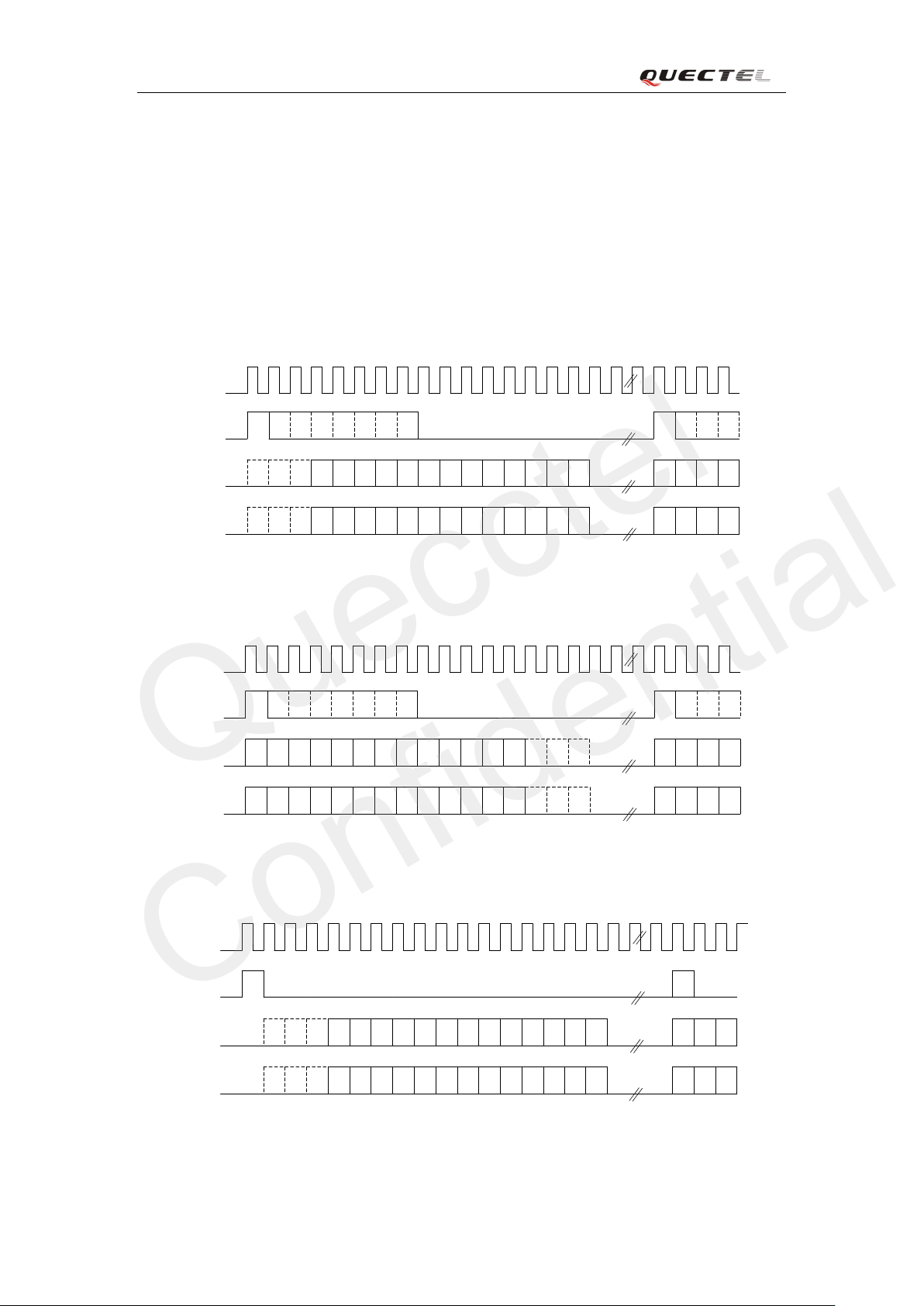
M50 Hardware Design
12 11 10 9 8 7 6 5 4 3 2 1 0
12 11 10 9 8 7 6 5 4 3 2 1 0
PCM_CLK
PCM_SYNC
PCM_OUT
PCM_IN
MSB
MSB
Sign extension
Sign extension
12 11 10 9 8 7 6 5 4 3 2 1 0
12 11 10 9 8 7 6 5 4 3 2 1 0
PCM_CLK
PCM_SYNC
PCM_OUT
PCM_IN
MSB
MSB
Zero padding
Zero padding
PCM_CLK
PCM_SYNC
PCM_OUT
PCM_IN
12 11 10 9 8 7 6 5 4 3 2 1 0
12 11 10 9 8 7 6 5 4 3 2 1 0
MSB
MSB
Sign extension
Sign extension
Quecctel
Confidential
3.13.2. Timing
The sample rate of the PCM interface is 8 KHz and the clock source is 256 KHz, so every frame
contains 32 bits data, since M50 sup po rts 16 bits line code PCM format, the left 16 bits are invalid.
The following diagra m shows the timing of diffe rent com bi n a ti o ns . The synchronization length in
long synchronization format can be programmed by fi rmware from one bit to eight bits. In the
Sign extension mode, the high three bits of 16 bits are sign extension, and in the Zero padding
mode, the low three bits of 16 bits are zero padding.
Figure 38: Long synchronization & Sig n extension diagram
Figure 39: Long synchronizati on & Zero padding diagram
Figure 40: Short synchronization & Sign extension diagram
M50_HD_V2.0 - 63 -
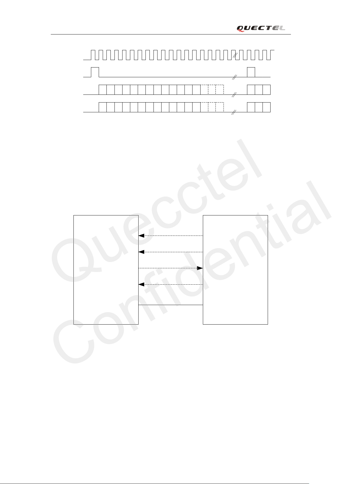
M50 Hardware Design
PCM_CLK
PCM_SYNC
PCM_OUT
PCM_IN
12 11 10 9 8 7 6 5 4 3 2 1 0
12 11 10 9 8 7 6 5 4 3 2 1 0
MSB
MSB
Zero padding
Zero padding
PCM_SYNC
PCM_CLK
PCM_OUT
PCM_IN
PCM_SYNC
PCM_CLK
PCM_IN
PCM_OUT
Module
(master)
Codec
(slave)
GND
GND
Quecctel
Confidential
Figure 41: Short synchronization & Zero padding diagram
3.13.3. Reference design
As M50 only acts as a master, the module provides synchronization and clock source. The
reference design is shown as below.
Figure 42: Reference design for PCM
3.13.4. AT command
There are two AT commands about the configuration of PCM are listed as below.
“AT+QPCMON” can configure operating mode of PCM.
AT+QPCMON= mo de ,Sync_Type,Sync_Length,SignExtension,MSBFirst
M50_HD_V2.0 - 64 -

M50 Hardware Design
Quecctel
Confidential
Table 23: QPCMON comm and desc riptio n
Parameter scope Description
Mode 0~2 0: Close PCM
1: Open PCM
2: Open PCM w hen audi o t al k is set up
Sync_Type 0~1 0: Short synchronization
1: Long synchronization
Sync_Length 1~8 Programme d fr om one bit to eight bit
SignExtension 0~1 0: Zero padding
1: Sign extension
MSBFirst 0~1 0: MSB first
1: Not supported
“AT+QPCMVOL” can configure volume of input and output.
AT+QPCMVOL=vol_pcm_in,vol_pcm_out
Table 24: QPCMVOL command description
Parameter scope Description
vol_pcm_in 0~32767 Set the input volume
vol_pcm_out 0~32767 Set the output volume
The voice may be distorted when this
val ue exceeds 163 84.
M50_HD_V2.0 - 65 -

M50 Hardware Design
Quecctel
Confidential
3.14. ADC
The module provides two ADC channel to measure the value of vol t a ge . Please give priority to the
use of ADC 0 channe l. The command “AT+QADC” can re ad t he v olt age v alue applied o n ADC 0
pin, while AT command “AT +QEADC” can re ad the v oltage value applied o n ADC1 pin. For
details of thi s AT com ma nd, ple ase re fer t o the document [1]. In order t o i mprove the accuracy of
ADC, the layout of ADC should be surrounded by gro und.
Table 25: Pin definition of the ADC
Name Pin Description
ADC0 2 General purpose analog t o digit al c on ve rter
ADC1 1 General purpose anal o g to digit al converter
Table 26: Char acteris ti c s of the ADC
Parameter Min Typ Max Unit
Voltage Range 0 2.8 V
ADC Resolution 10 bit
ADC Accuracy 2.7 mV
3.15. Behaviors of the RI
Table 27: Behaviors of the RI
State RI response
Standby HIGH
Voice c al l in g Change to LOW, then:
1. Cha n ge to HIGH when call is es ta bl ishe d.
2. Use AT H to h an g up t he cal l , RI changes to HIG H.
3. Calling part hangs up, RI changes t o HIG H first, and ch ange s t o LOW for
120ms indicating “NO CARRIER” as an URC, then changes t o HIGH
again.
4. Cha n ge to HIGH when SMS is recei ved.
Data cal ling Change to LOW, then:
1. Cha n ge to HIGH when dat a connecti o n i s established .
2. Use AT H t o hang up the d ata calli n g, RI changes to HIG H.
3. Calling part hangs up, RI changes t o HIG H first, and ch ange s t o LOW for
120ms indicating “NO CARRIER” as an URC, then changes t o HIGH
again.
M50_HD_V2.0 - 66 -
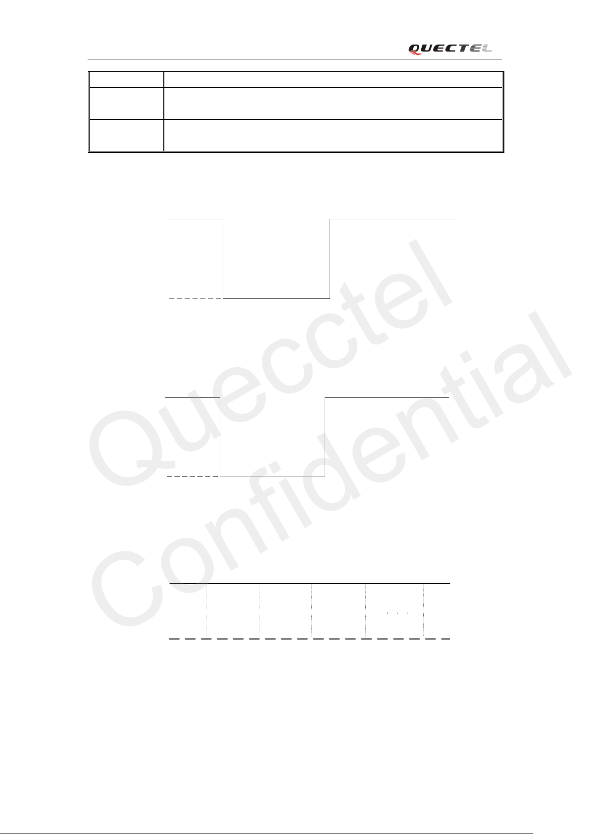
M50 Hardware Design
RI
Idle Ring
Off-hook by“ATA”
On-hook by “ATH”
SMS received
HIGH
LOW
RI
Idle Ring
Data calling establish
SMS received
HIGH
LOW
On-hook by “ATH”
RI
Idle Calling
On-hook
Talking
HIGH
LOW
Idle
Quecctel
Confidential
4. Cha n ge to HIGH when SMS is recei ved.
SMS Whe n a ne w SMS comes, the RI change s to LO W and holds lo w leve l for
about 12 0 ms, then c h an ge s t o HI G H .
URC Certain URCs can trigger 120ms low level on RI. For more details, ple ase
refer to the document [1]
If the mod ule is us ed as a caller, the RI would m aintai n high except the URC or SMS is received.
On the other hand, when it is used as a receiver, the timing of the RI is shown below.
Figure 43: RI behavior of voice calling as a receiver
Figure 44
: RI behavior of data cal li ng as a rec e iver
M50_HD_V2.0 - 67 -
Figure 45
: RI behavior as a caller

M50 Hardware Design
RI
Idle or
Talking
URC or
SMS received
HIGH
LOW
120ms
Quecctel
Confidential
Figure 46:
RI behavior of URC or SMS received
M50_HD_V2.0 - 68 -

M50 Hardware Design
Module
300R
4.7K
47K
VBAT
NETLIGHT
Quecctel
Confidential
3.16. Network status indication
The N E T LIGHT signal can be u se d to dri ve a ne twork status indicator LED. The working state of
this pin is listed in th e following table.
Table 28: Work ing state of th e NETLIGHT
State Module function
Off The module is not running.
64ms On/ 800ms Off The module is not synchronized with network.
64ms On/ 2000ms Off The module is syn c h ro ni z ed with network.
64ms On/ 600ms Off GPRS data transfer is ongoing.
A re fe r en ce cir cuit is shown as below.
Figure 47: Reference design for NETLIGHT
3.17. Operating stat us in dication
The STAT U S pin is set as an output pin and can be us ed to judge whether module is power-on. In
customer’s de sign, thi s pin can be conne cted t o a GPIO of D TE or be use d to drive an LE D in
order to judge the module’s operation status. A reference ci r c u it is shown in Figure 48.
Table 29: Pin definition of the STATUS
Name Pin Description
STAT US 16 Indicate module operating status
M50_HD_V2.0 - 69 -

M50 Hardware Design
Module
300R
4.7K
47K
VBAT
STATUS
Quecctel
Confidential
Figure 48: Reference design for STATUS
M50_HD_V2.0 - 70 -

M50 Hardware Design
Module
RF_ANT
0R
NM NM
Quecctel
Confidential
4. Antenna int erface
The Pin 63 is the RF antenna pad. The RF interface has an impedance of 50Ω.
Table 30: Pin definition of the RF_ANT
Name Pin Description
GND 61 Ground
GND 62 Ground
RF_ANT 63 RF antenna pad
GND 64 Ground
GND 65 Ground
GND 66 Ground
4.1. RF ref e rence desi gn
The reference design for RF is shown as below.
Figure 49: Reference design for RF
M50 provides an RF anten na pad for cust omer ’s ant enna connection. The RF trace in h ost PCB
connected to the module RF antenna pad should be micro-strip line or othe r types of RF t race ,
whose characteristi c impedance s h ould be clo se to 50Ω. M50 comes with gro undin g pads which
are next t o the antenna p ad i n o rde r to gi ve a be tter grou n ding. Besides, a ∏ type match circuit is
suggested to be used to adjust the RF performance.
To minimize the loss on the RF trace and RF cable, take design into account carefully. It is
recommended that the insertion loss should meet the following requirements:
M50_HD_V2.0 - 71 -

M50 Hardware Design
Quecctel
Confidential
GSM850/EGSM900 is <1dB.
DCS1800/PCS1900 is <1.5dB.
4.2. RF output power
Table 31: The module conducted RF output power
Frequency Max Min
GSM850 32.5dBm ±1dB 5dBm±5dB
EGSM900 32.5dBm ±1dB 5dBm±5dB
DCS1800 29.5dBm ±1dB 0dBm±5dB
PCS1900 29.5dBm ±1dB 0dBm±5dB
Note: In GSM850&EGSM900 GPRS 4 slots TX mode, the max output power is reduced by
2.5dB. This design con f orms to t he GSM spe c ificati on as des c ribed in section 13.16 of 3G P P TS
51.010-1.
4.3. RF receiving sensitivity
Table 32: The module conducted RF receiving sensitivity
Frequency Receive sensitivity
GSM850 < -108.5dBm
EGSM900 < -108.5dBm
DCS1800 < -108.5dBm
PCS1900 < -108.5dBm
4.4. Operating frequen c ies
Table 33: The module operating frequencies
Frequency Receive Transmit ARFCH
GSM850 869~894MHz 824~849MHz 128~251
EGSM900 925~960MHz 880~915MHz 0~124, 975~1023
DCS1800 1805~1880MHz 1710~1785MHz 512~885
PCS1900 1930~1990MHz 1850~1910MHz 512~810
M50_HD_V2.0 - 72 -

M50 Hardware Design
Quecctel
Confidential
4.5. RF cable soldering
Soldering the RF cable to RF pad of module correctly will re duce t he loss on the path of RF,
please refer to the follo wing example of RF soldering.
Figure 50: RF soldering sample
M50_HD_V2.0 - 73 -
M50 Hardware Design
Quecctel
Confidential
5. Electrical, reliability and radio characteristics
5.1. A bsolute maximum ratings
Absol ute m axim um ratings for p o wer s u pply an d voltage o n digit al a nd a nalog pins o f mo du l e a r e
listed in the following table:
Table 34: Absolut e m a xim um ratin g s
Parameter Min Max Unit
VBAT -0.3 +4.73 V
Peak current of power supply 0 2 A
RMS curr e nt of powe r supply ( during one TDMA- frame) 0 0.7 A
Voltage at digital pins -0.3 3.3 V
Voltage at analog pins -0.3 3.0 V
Voltage at digital/analog pins in power down mode -0.25 0.25 V
5.2. Operating temperature
The operating temperature is listed in the following table:
Table 35: Oper ating temperature
Parameter Min Typ Max Unit
Normal Temperature -35 +25 +80 ℃
Restricted Operation1) -40 ~ -35 +80 ~ +85 ℃
Storage Temperature -45 +90 ℃
1)When the module works in this temperature range, the deviation from the GSM specification
may occur. For example, the frequency error or the phase error will be increased.
M50_HD_V2.0 - 74 -

M50 Hardware Design
50
Quecctel
Confidential
5.3. Power supply ratings
Table 36: The module po wer suppl y ratings
Parameter Description Conditions Min Typ Max Unit
VBAT Supply
voltage
Voltage must stay within the
min/max values, including
volt age dr op, rippl e , an d spikes.
3.3 4.0 4.6 V
Vdrop during
transmitting
burst
Voltage
ripple
I
VBAT
Average
supply
current
Maximum pow er contr ol lev el
on GSM850 and GSM90 0.
Maximum power control level
on GSM850 and GSM90 0
@ f<200kHz
@ f>200kHz
Power down mode
SLEEP mode @ DRX=5
Minim um fun ctionality mode
AT+CFUN=0
IDLE mode
SL EEP mode
AT+CFUN=4
IDLE mode
SL EEP mode
IDLE mode
GSM850/EGSM 900
DCS1800/PCS1900
TALK mode
1)
GSM850/EGSM 900
DCS1800/PCS1900
DAT A mode , GPRS (3 Rx,2T x)
GSM850/EGSM 900
DCS1800/PCS1900
DATA m od e , GPRS(2 Rx,3Tx)
GSM850/EGSM 900
DCS1800/PCS1900
DAT A mode , GPRS (4 Rx,1T x)
GSM850/EGSM 900
DCS1800/PCS1900
DATA m od e , GPRS
(1Rx,4Tx)
GSM850/EGSM 9001)
2)
1)
2)
1)
2)
1)
2)
400 mV
30
1.3
13
0.98
13
1.0
13
13
209/208
191/202
435/400
313/337
605/558
399/460
265/240
200/212
615/560
2
mV
mV
uA
mA
mA
mA
mA
mA
mA
mA
mA
mA
mA
mA
mA
mA
mA
mA
mA
M50_HD_V2.0 - 75 -

M50 Hardware Design
Quecctel
Confidential
DCS1800/PCS19002) 420/470 mA
Peak supply
current
(during
transmission
slot)
1)
Power control level PCL 5
2)
Power control level PCL 0
5.4. Current consumption
The values of current consumption are shown as below.
Table 37: The module current consumption
Condition Current Consumption
Voice Call
GSM850 @power level #5 <300mA,Typic al 209mA
GSM900 @power level #5 <300mA,Typical 208mA
DCS1800 @power level #0 <250mA,Typical 191mA
PCS1900 @power level #0 <250mA,Typical 202mA
GPRS Data
DATA mode, GPRS ( 1 Rx,1 Tx ) CLASS 12
GSM850 @power level #5 <350mA,Typical 199mA
EGSM 9 0 0 @power level #5 <350mA,Typical 200mA
DCS 1800 @power level #0 <300mA,Typical 184mA
PCS 1900 @power level #0 <300mA,Typical 192mA
Maximum power control level
on GSM850 and GSM90 0.
@power level #12,Typical 96mA
@power level #19,Typical 73mA
@power level #12,Typical 96mA
@power level #19,Typical 73mA
@power level #7,Typical 93mA
@power level #15,Typical 70mA
@power level #7,Typical 95mA
@power level #15,Typical 71mA
@power level #12,Typical 87mA
@power level #19,Typical 63mA
@power level #12,Typical 96mA
@power level #19,Typical 70mA
@power level #7,Typical 82mA
@power level #15,Typical 66mA
@power level #7,Typical 82mA
@power level #15,Typical 66mA
1.6 1.8 A
M50_HD_V2.0 - 76 -
M50 Hardware Design
Quecctel
Confidential
DATA mode, GPRS ( 3 Rx, 2 Tx ) CLASS 12
GSM850 @power level #5 <550mA,Typical 435mA
@power level #12,Typical 158mA
@power level #19,Typical 99mA
EGSM 9 0 0 @power level #5 <550mA,Typical 400mA
@power level #12,Typical 150mA
@power level #19,Typical 97mA
DCS 1800 @power level #0 <450mA,Typical 313mA
@power level #7,Typical 130mA
@power level #15,Typical 92mA
PCS 1900 @power level #0 <450mA,Typical 337mA
@power level #7,Typical 140mA
@power level #15,Typical 94mA
DATA m od e , GPRS ( 2 Rx, 3 Tx ) CL ASS 1 2
GSM850 @power level #5 <640mA,Typical 605mA
@power level #12,Typical 195mA
@power level #19,Typical 107mA
EGSM 9 0 0 @power level #5 <600mA,Typical 558mA
@power level #12,Typical 185mA
@power level #19,Typical 106mA
DCS 1800 @power level #0 <490mA,Typical 399mA
@power level #7,Typical 150mA
@power level #15,Typical 94mA
PCS 1900 @power level #0 <480mA,Typical 460mA
@power level #7,Typical 166mA
@power level #15,Typical 98mA
DATA mode, GPRS ( 4 Rx,1 Tx ) CLASS 12
GSM850 @power level #5 <350mA,Typical 265mA
@power level #12,Typical 122mA
@power level #19,Typical 93mA
EGSM 9 0 0 @power level #5 <350mA,Typical 240mA
@power level #12,Typical 115mA
@power level #19,Typical 90mA
DCS 1800 @power level #0 <300mA,Typical 200mA
@power level #7,Typical 107mA
@power level #15,Typical 89mA
PCS 1900 @power level #0 <300mA,Typical 212mA
DATA m od e , GPRS ( 1 Rx, 4 Tx ) CL ASS 1 2
GSM850 @power level #5 <660mA,Typical 615mA
@power level #7,Typical 118mA
@power level #15,Typical 90mA
@power level #12,Typical 232mA
@power level #19,Typical 118mA
M50_HD_V2.0 - 77 -
M50 Hardware Design
Quecctel
Confidential
EGSM 9 0 0 @power level #5 <660mA,Typical 560mA
@power level #12,Typical 215mA
@power level #19,Typical 114mA
DCS 1800 @power level #0 <530mA,Typical 420mA
@power level #7,Typical 173mA
@power level #15,Typical 97mA
PCS 1900 @power level #0 <530mA,Typical 470mA
@power level #7,Typical 192mA
@power level #15,Typical 101mA
Note: GPRS Class 12 is the default setting. The module can be configured from G P RS Class 1
to Cl ass 12 by “AT+QGPCLASS”. Setting to lower GPRS cl ass woul d make it eas ier to design
the power s upply for the module.
5.5. Electro-static discharge
Although the GSM engine is generally protected against Electrostatic Discharge (ESD), ESD
protection precautions should still be emphasized. Pr oper ESD h an dling and packaging procedures
must be appli ed th rough out the proce ssin g, handli ng and oper ati on of any applications using the
module.
The measured ESD valu es of modu le are shown in the following table.
Table 38: The ESD endurance (Temperature:25℃,Humidity:45 %)
Tested point Contact
discharge
VBAT,GND ±5KV ±10KV
RF_ANT ±5KV ±10KV
PWRKEY
STAT US
SIM_VDD, SIM_DATA
SIM_CLK, SIM_RST
TXD, RXD
RTS, CTS, DTR
Others ±0.5KV ±1KV
±2KV ±4KV
±2KV ±4KV
±2KV ±4KV
Air d i s charg e
M50_HD_V2.0 - 78 -
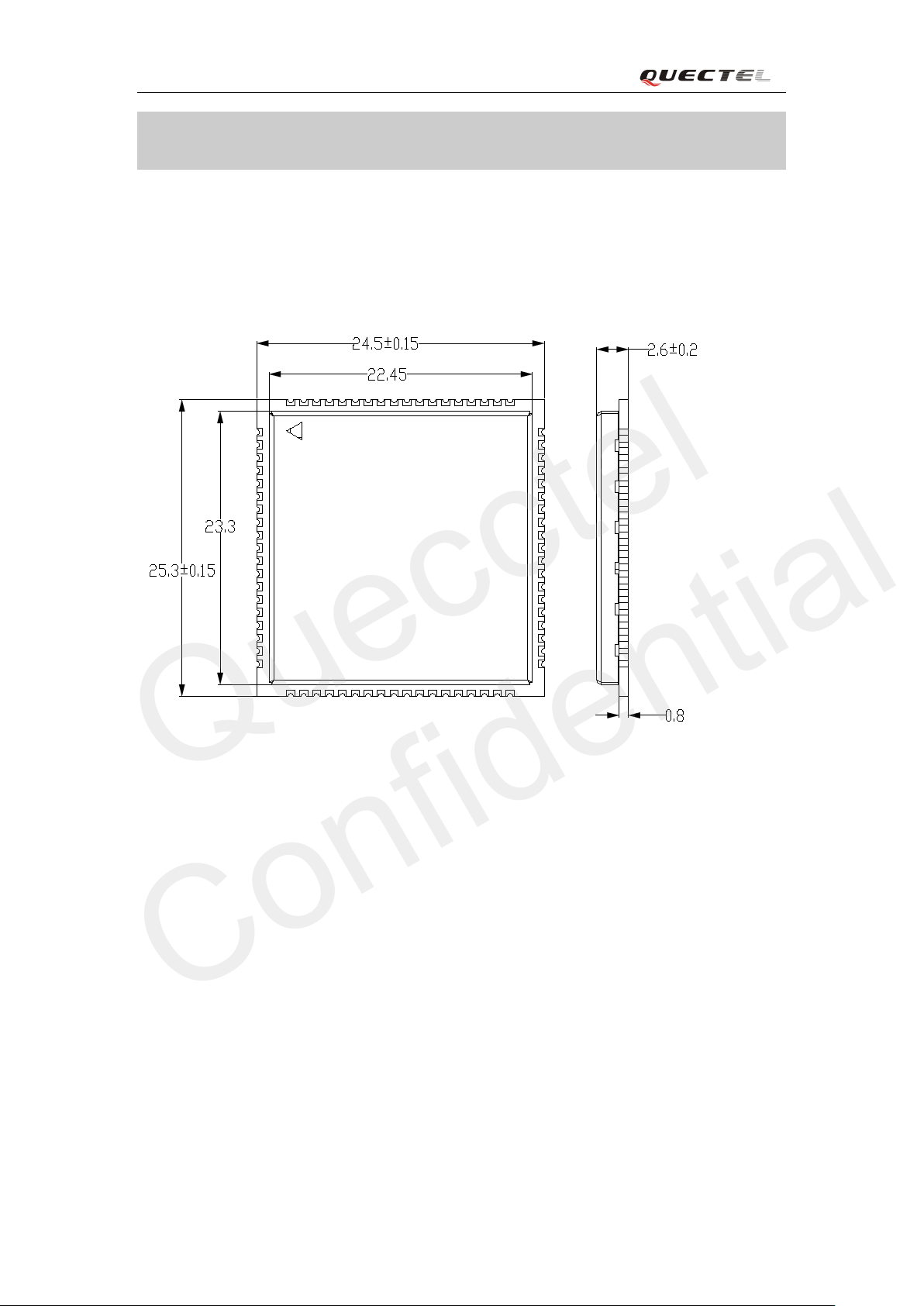
M50 Hardware Design
Quecctel
Confidential
6. Mechani cal dim ensions
This c h apter des c ribes the mechanical dimensi o ns of the mod ul e .
6.1. M e c hanical dime nsions of mo d ul e
Figure 51: M50 top and side dimensions
M50_HD_V2.0 - 79 -

M50 Hardware Design
Quecctel
Confidential
Figure 52:
M50 bottom dimensions
M50_HD_V2.0 - 80 -

M50 Hardware Design
silkscreen
frame line
Quecctel
Confidential
6.2. Recommended footprint withou t bottom centre pad s
Figure 53: Recommended footprint without bottom centre pads
M50_HD_V2.0 - 81 -

M50 Hardware Design
Quecctel
Confidential
6.4. Top view of the module
Figure 54: Top view of the module
M50_HD_V2.0 - 82 -
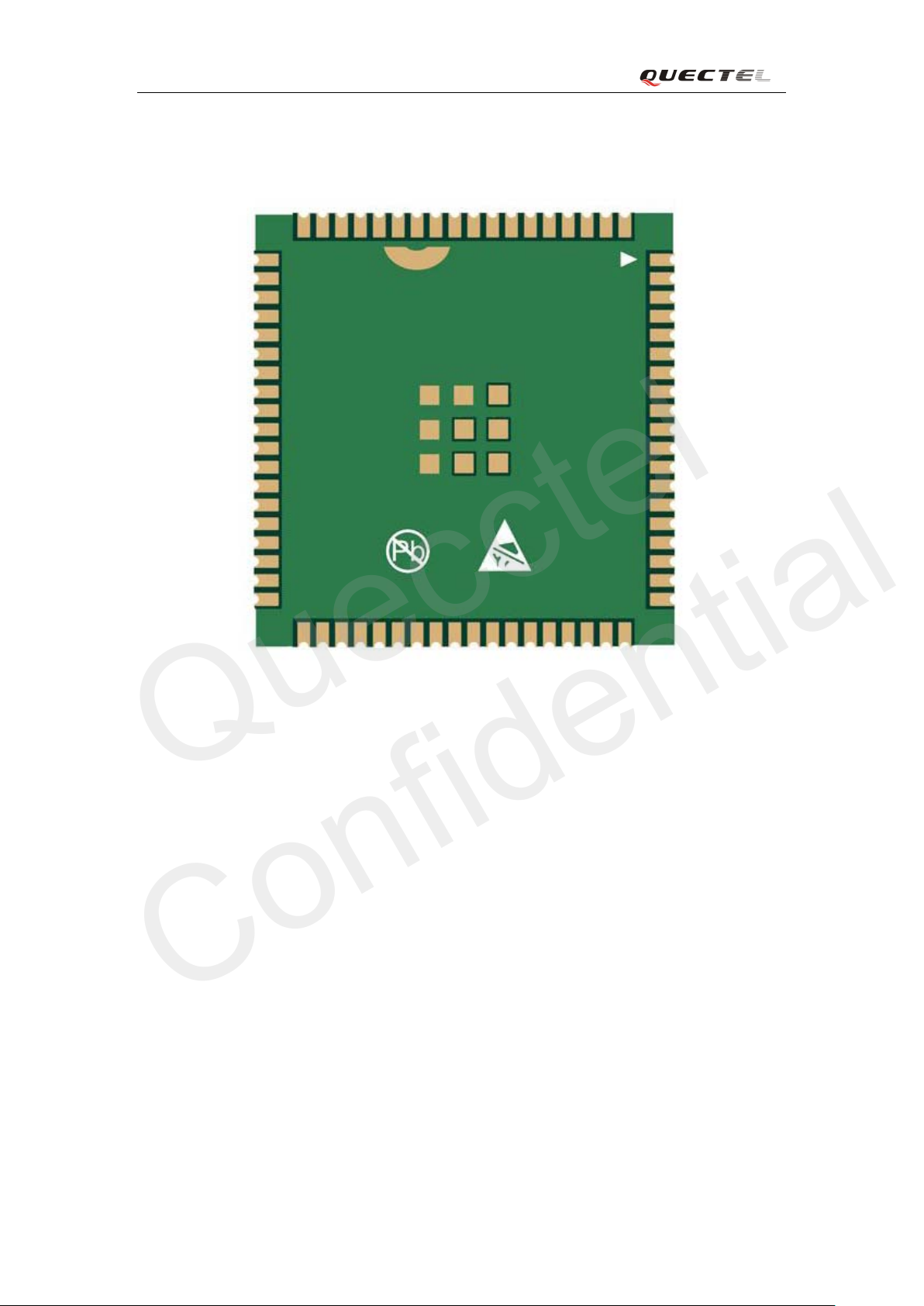
M50 Hardware Design
Quecctel
Confidential
6.5. Bottom view of the module
Figure 55: Bottom view of the module
M50_HD_V2.0 - 83 -

M50 Hardware Design
Quecctel
Confidential
7. Storage and manufacturing
7.1. Storage
M50 is distributed in vacuum-sealed bag. The restriction of storage c on di tion is sh own as below.
Shelf life in sealed bag: 12 months at <40℃/90% RH
After this bag is opened, devices that will be subjected to reflow solder or other high temperature
process must be:
Mounted within 72 hours at factory c on di tions of ≤30℃/60% RH
Stored at <10% RH
Devices require bake b efore mounting, if:
Humidit y i ndicator card is > 1 0% w hen read at 23℃±5℃
Mounted exceed 72 hours at factory conditions of ≤30 ℃/ 6 0% RH
If baking is required, devices may be baked for 48 hours at 125℃±5℃
Note: As plastic container cannot be subjected to high temperature, devices must be removed
℃
prior to high temperature (125
IPC/JEDECJ-STD-033 for bake proce dure.
) bake. If shorter bake times are desired, refer to the
M50_HD_V2.0 - 84 -

M50 Hardware Design
Quecctel
Confidential
7.2. Soldering
The squeegee should push the paste on t he surface of the stencil that makes the paste fill the
sten cil openi ngs and pene t rate t o t he PC B. The fo rce o n the sq uee gee s ho uld be adj us ted so as t o
produce a clean stencil surface on a single pass. To ensure the module soldering quality, the
thickness of stencil at the hole of the module pads should be 0.2mm for M50 .
Figure 56: Paste application
Suggest peak reflow temperature is from 235℃ to 245℃ (for SnAg3.0Cu0.5 alloy). Absolute
max reflow temperature is 260℃. T o avoid d a m a ge t o the module when it w as repeatedly heated,
it is s uggest ed that t he modu le sho uld be m ounted after the first panel h as been reflowed . The
follow ing picture is the actual dia gr a m w hi c h we have operated.
M50_HD_V2.0 - 85 -

M50 Hardware Design
Time(s)
50
100
150 200 250 300
50
100
150
200
250
160℃
200℃
217
0
70s~120s
40s~60s
Between 1~3℃/S
Preheat
Heating
Cooling
℃
s
Liquids Temperature
Quecctel
Confidential
Figure 57: Ramp-Soak-Spike reflow profile
7.3. Packaging
M50 module s are distributed in tr ays of 20 pie ces e ac h. This is e spe ciall y suit able for t he M50
according to SMT processes requirements.
The trays a re st ore d ins ide a vacuum-sealed bag whi ch is ESD pr ot ected. It should no t be opene d
until the devices are ready to be soldered onto the application.
Figure 58: Module tray
M50_HD_V2.0 - 86 -

M50 Hardware Design
Rate 1/2 convolutional coding
Puncturing
Quecctel
Confidential
Appendix A: GPRS coding schemes
Four coding schemes are used in GPRS protocol. The differences between them are shown in
Table 39.
Table 39: Description of different coding schemes
Scheme Code
rate
CS-1 1/2 3 3 181 40 4 456 0 9.05
CS-2 2/3 3 6 268 16 4 588 132 13.4
CS-3 3/4 3 6 312 16 4 676 220 15.6
CS-4 1 3 12 428 16 - 456 - 21.4
Radio block structure of CS-1, CS-2 and CS-3 is shown a s Figure 60:
USF Pre-coded
USF
USF
Radio
Block
excl.USF
and BCS
Radio Block
456 bits
BCS Tail Coded
bits
Punctured
bits
BCS
Data
rate
Kb/s
Radio block structure of CS-4 is shown as Figure 61:
M50_HD_V2.0 - 87 -
Figure 59: Radio block structure of CS-1, CS-2 and CS-3
Radio Block
USF
Block
code
Figure 60: Radio block structure of CS-4
No coding
456 bits
BCS

M50 Hardware Design
Quecctel
Confidential
Appendix B: GPRS multi-slot classes
Twenty-nine classes of GPRS multi-slot modes are defined for MS in GPRS specification.
Multi-slot classes are product dependant, and determine the maximum achievable data rates in
both the uplink and downlink directions. Written as 3+1 or 2+2, the first numbe r i ndicates the
amount of d ownlink ti meslot s, while the se cond nu m be r indi cat es t he amount of upli n k t imesl ot s .
The a ctive sl ots dete rmine t he total nu mber of slots t he GPRS de vice can use simul tane ousl y for
both uplink and downlink communications. The description of different multi-slot classes is
show n in Tab l e 40.
Table 40: GPRS multi-slot classes
Multislot class Downlink slots U pl in k s lots Active slots
1 1 1 2
2 2 1 3
3 2 2 3
4 3 1 4
5 2 2 4
6 3 2 4
7 3 3 4
8 4 1 5
9 3 2 5
10 4 2 5
11 4 3 5
12 4 4 5
M50_HD_V2.0 - 88 -

Quecctel
Confidential
Room 501, Building 13, No.99 Ti anzhou Road, Shanghai, China 200233
Sha nghai Quectel Wireless Solutions Co., Ltd.
Tel: +86 21 5108 6236
Mail: info@quectel.com
 Loading...