


M26 Hardware Design
GSM/GPRS Module Series
Rev. M26_Hardware_Design_V1.1
Date: 2014-11-24
www.quectel.com

GSM/GPRS Module Series
M26 Hardware Design
Our aim is to provide customers with timely and comprehensive service. For any assistance, please contact our company headquarters:
Quectel Wireless Solutions Co., Ltd.
Office 501, Building 13, No.99, Tianzhou Road, Shanghai, China, 200233
Tel: +86 21 5108 6236
Mail: info@quectel.com
Or our local office, for more information, please visit:
http://www.quectel.com/support/salesupport.aspx
For technical support, to report documentation errors, please visit: http://www.quectel.com/support/techsupport.aspx
GENERAL NOTES
QUECTEL OFFERS THIS INFORMATION AS A SERVICE TO ITS CUSTOMERS. THE INFORMATION
PROVIDED IS BASED UPON CUSTOMERS’ REQUIREMENTS. QUECTEL MAKES EVERY EFFORT
TO ENSURE THE QUALITY OF THE INFORMATION IT MAKES AVAILABLE. QUECTEL DOES NOT MAKE ANY WARRANTY AS TO THE INFORMATION CONTAINED HEREIN, AND DOES NOT ACCEPT ANY LIABILITY FOR ANY INJURY, LOSS OR DAMAGE OF ANY KIND INCURRED BY USE OF OR RELIANCE UPON THE INFORMATION. ALL INFORMATION SUPPLIED HEREIN IS SUBJECT TO CHANGE WITHOUT PRIOR NOTICE.
COPYRIGHT
THIS INFORMATION CONTAINED HERE IS PROPRIETARY TECHNICAL INFORMATION OF QUECTEL CO., LTD. TRANSMITTABLE, REPRODUCTION, DISSEMINATION AND EDITING OF THIS DOCUMENT AS WELL AS UTILIZATION OF THIS CONTENTS ARE FORBIDDEN WITHOUT PERMISSION. OFFENDERS WILL BE HELD LIABLE FOR PAYMENT OF DAMAGES. ALL RIGHTS ARE RESERVED IN THE EVENT OF A PATENT GRANT OR REGISTRATION OF A UTILITY MODEL OR DESIGN.
Copyright © Quectel Wireless Solutions Co., Ltd. 2014. All rights reserved.
M26_Hardware_Design |
Confidential / Released |
1 / 80 |

GSM/GPRS Module Series
M26 Hardware Design
About the Document
History
|
Revision |
|
|
Date |
|
Author |
|
|
Description |
|
|
|
|
|
|
|
|
|
|||||
|
|
|
|
|
|
|
|||||
|
|
|
|
|
|
|
|
|
|
|
|
|
|
|
|
|
|
|
|
|
|
||
1.0 |
|
2014-08-07 |
|
Felix YIN |
|
Initial |
|||||
|
|
|
|
|
|
|
|
|
|
||
|
|
|
|
|
|
|
|
1. |
Modified output power of Bluetooth |
||
|
|
|
|
|
|
|
|
2. |
Modified the timing of the RFTXMON signal |
||
|
|
|
|
|
|
|
|
3. |
Updated Figure 5: Reference circuit for power |
||
|
|
|
|
|
|
|
|
|
|
supply |
|
|
|
|
|
|
|
|
|
4. |
Modified description of RTC and SIM card |
||
1.1 |
|
2014-11-24 |
|
Felix YIN |
|
|
interface |
||||
|
|
5. |
Modified description of UART Application |
||||||||
|
|
|
|
|
|
|
|
||||
|
|
|
|
|
|
|
|
6. |
Deleted the over-voltage automatic shutdown |
||
|
|
|
|
|
|
|
|
|
|
function |
|
|
|
|
|
|
|
|
|
7. |
Modified the antenna gain in the Table 24 |
||
|
|
|
|
|
|
|
|
8. |
Modified the current consumption information in |
||
|
|
|
|
|
|
|
|
|
|
Section 5.3 & 5.4 |
|
|
|
|
|
|
|
|
|
|
|
|
|
M26_Hardware_Design |
Confidential / Released |
2 / 80 |

GSM/GPRS Module Series
M26 Hardware Design
Contents
About the Document................................................................................................................................... |
|
2 |
|||
Contents ....................................................................................................................................................... |
|
|
3 |
||
Table Index................................................................................................................................................... |
|
|
6 |
||
Figure Index ................................................................................................................................................. |
|
|
7 |
||
1 |
Introduction |
.......................................................................................................................................... |
|
9 |
|
|
1.1. |
Safety Information.................................................................................................................... |
10 |
||
2 |
Product Concept ................................................................................................................................ |
|
11 |
||
|
2.1. |
General Description................................................................................................................. |
11 |
||
|
2.2. |
Key Features |
........................................................................................................................... |
12 |
|
|
2.3. |
Functional Diagram ................................................................................................................. |
14 |
||
|
2.4. |
Evaluation Board ..................................................................................................................... |
14 |
||
3 |
Application Interface ......................................................................................................................... |
15 |
|||
|
3.1. |
Pin of Module........................................................................................................................... |
16 |
||
|
|
3.1.1. |
Pin Assignment .............................................................................................................. |
16 |
|
|
|
3.1.2. |
Pin Description ............................................................................................................... |
17 |
|
|
3.2. |
Operating Modes ..................................................................................................................... |
21 |
||
|
3.3. |
Power Supply........................................................................................................................... |
22 |
||
|
|
3.3.1. Power Features of Module............................................................................................. |
22 |
||
|
|
3.3.2. Decrease Supply Voltage Drop...................................................................................... |
23 |
||
|
|
3.3.3. Reference Design For Power Supply ............................................................................ |
23 |
||
|
|
3.3.4. |
Monitor Power Supply .................................................................................................... |
24 |
|
|
3.4. Power On and Down Scenarios .............................................................................................. |
24 |
|||
|
|
3.4.1. |
Power On ....................................................................................................................... |
24 |
|
|
|
3.4.2. |
Power Down ................................................................................................................... |
26 |
|
|
|
3.4.2.1. |
Power Down Module Using the PWRKEY Pin.................................................. |
26 |
|
|
|
3.4.2.2. |
Power Down Module Using AT Command ........................................................ |
27 |
|
|
|
3.4.2.3. |
Under-voltage Automatic Shutdown.................................................................. |
28 |
|
|
|
3.4.3. |
Restart ............................................................................................................................ |
|
28 |
|
3.5. |
Power Saving........................................................................................................................... |
29 |
||
|
|
3.5.1. |
Minimum Functionality Mode ......................................................................................... |
29 |
|
|
|
3.5.2. |
SLEEP Mode.................................................................................................................. |
29 |
|
|
|
3.5.3. Wake Up Module From SLEEP Mode ........................................................................... |
30 |
||
|
|
3.5.4. |
Summary of State Transition.......................................................................................... |
30 |
|
|
3.6. |
RTC Backup............................................................................................................................. |
|
30 |
|
|
3.7. |
Serial Interfaces....................................................................................................................... |
32 |
||
|
|
3.7.1. |
UART Port ...................................................................................................................... |
34 |
|
|
|
3.7.1.1. |
The Feature of UART Port................................................................................. |
34 |
|
|
|
3.7.1.2. |
The Connection of UART .................................................................................. |
35 |
|
M26_Hardware_Design |
Confidential / Released |
3 / 80 |

|
|
|
|
|
|
GSM/GPRS Module Series |
|
|
|
|
|
|
M26 Hardware Design |
|
|
|
|
|
|
|
|
|
|
|
|
|
|
|
|
|
3.7.1.3. |
Firmware Upgrade ............................................................................................. |
36 |
|
|
3.7.2. |
|
Debug Port ..................................................................................................................... |
37 |
||
|
3.7.3. |
|
Auxiliary UART Port ....................................................................................................... |
38 |
||
|
3.7.4. |
|
UART Application ........................................................................................................... |
38 |
||
|
3.8. |
|
Audio Interfaces....................................................................................................................... |
40 |
||
|
|
3.8.1. Decrease TDD Noise and other Noise .......................................................................... |
41 |
|||
|
3.8.2. |
|
Microphone Interfaces Design ....................................................................................... |
41 |
||
|
|
3.8.3. Receiver and Speaker Interface Design ........................................................................ |
42 |
|||
|
3.8.4. |
|
Earphone Interface Design ............................................................................................ |
44 |
||
|
3.8.5. |
|
Audio Characteristics ..................................................................................................... |
44 |
||
|
3.9. |
|
PCM Interface.......................................................................................................................... |
45 |
||
|
3.9.1. |
|
Configuration .................................................................................................................. |
45 |
||
|
3.9.2. |
|
............................................................................................................................. |
46 |
||
|
3.9.3. |
|
Reference .......................................................................................................... Design |
48 |
||
|
3.9.4. |
|
AT Command ................................................................................................................. |
48 |
||
|
3.10. |
SIM Card Interface................................................................................................................... |
49 |
|||
|
3.11. |
ADC |
|
51 |
||
|
3.12. |
Behaviors of .................................................................................................................The RI |
51 |
|||
|
3.13. |
Network ........................................................................................................Status Indication |
53 |
|||
|
3.14. |
RF Transmitting ............................................................................................Signal Indication |
54 |
|||
4 |
Antenna Interface............................................................................................................................... |
|
56 |
|||
|
4.1. |
|
GSM ...........................................................................................................Antenna Interface |
56 |
||
|
4.1.1. |
.......................................................................................................... |
Reference Design |
56 |
||
|
4.1.2. |
........................................................................................................... |
RF Output Power |
57 |
||
|
4.1.3. |
................................................................................................ |
RF Receiving Sensitivity |
58 |
||
|
4.1.4. |
................................................................................................... |
Operating Frequencies |
58 |
||
|
4.1.5. |
........................................................................................................ |
RF Cable Soldering |
59 |
||
|
4.2. |
|
Bluetooth ....................................................................................................Antenna Interface |
59 |
||
5 Electrical, Reliability ............................................................................and Radio Characteristics |
61 |
|||||
|
5.1. |
|
Absolute .....................................................................................................Maximum Ratings |
61 |
||
|
5.2. |
|
Operating ............................................................................................................Temperature |
61 |
||
|
5.3. |
|
Power .............................................................................................................Supply Ratings |
62 |
||
|
5.4. |
|
Current ..............................................................................................................Consumption |
63 |
||
|
5.5. |
|
Electro ...........................................................................................................-static Discharge |
65 |
||
6 |
Mechanical ....................................................................................................................Dimensions |
66 |
||||
|
6.1. |
|
Mechanical ..........................................................................................Dimensions of Module |
66 |
||
|
6.2. |
|
Recommended .........................................................................................................Footprint |
68 |
||
|
6.3. |
|
Top View ...........................................................................................................of the Module |
69 |
||
|
6.4. |
|
Bottom ......................................................................................................View of the Module |
69 |
||
7 |
Storage and ..............................................................................................................Manufacturing |
70 |
||||
|
7.1. |
|
Storage..................................................................................................................................... |
|
70 |
|
|
7.2. |
|
Soldering.................................................................................................................................. |
|
71 |
|
M26_Hardware_Design |
Confidential / Released |
4 / 80 |

|
|
GSM/GPRS Module Series |
|
|
M26 Hardware Design |
|
7.3. Packaging ................................................................................................................................ |
71 |
|
7.3.1. Tape and Reel Packaging .............................................................................................. |
72 |
8 |
Appendix A Reference....................................................................................................................... |
73 |
9 |
Appendix B GPRS Coding Scheme ................................................................................................. |
78 |
10 |
Appendix C GPRS Multi-slot Class.................................................................................................. |
80 |
11 |
FCC Warning ...................................................................................................................................... |
81 |
M26_Hardware_Design |
Confidential / Released |
5 / 80 |

GSM/GPRS Module Series
M26 Hardware Design
Table Index |
|
TABLE 1: MODULE KEY FEATURES ............................................................................................................... |
12 |
TABLE 2: CODING SCHEMES AND MAXIMUM NET DATA RATES OVER AIR INTERFACE ........................ |
13 |
TABLE 3: IO PARAMETERS DEFINITION........................................................................................................ |
17 |
TABLE 4: PIN DESCRIPTION ........................................................................................................................... |
17 |
TABLE 5: OVERVIEW OF OPERATING MODES ............................................................................................. |
21 |
TABLE 6: SUMMARY OF STATE TRANSITION ............................................................................................... |
30 |
TABLE 7: LOGIC LEVELS OF THE UART INTERFACE .................................................................................. |
33 |
TABLE 8: PIN DEFINITION OF THE UART INTERFACES .............................................................................. |
33 |
TABLE 9: PIN DEFINITION OF AUDIO INTERFACE ....................................................................................... |
40 |
TABLE 10: TYPICAL ELECTRET MICROPHONE CHARACTERISTICS......................................................... |
44 |
TABLE 11: TYPICAL SPEAKER CHARACTERISTICS..................................................................................... |
44 |
TABLE 12: PIN DEFINITION OF PCM INTERFACE......................................................................................... |
45 |
TABLE 13: CONFIGURATION........................................................................................................................... |
45 |
TABLE 14: QPCMON COMMAND DESCRIPTION .......................................................................................... |
48 |
TABLE 15: QPCMVOL COMMAND DESCRIPTION......................................................................................... |
49 |
TABLE 16: PIN DEFINITION OF THE SIM INTERFACE .................................................................................. |
49 |
TABLE 17: PIN DEFINITION OF THE ADC ...................................................................................................... |
51 |
TABLE 18: CHARACTERISTICS OF THE ADC................................................................................................ |
51 |
TABLE 19: BEHAVIORS OF THE RI ................................................................................................................. |
51 |
TABLE 20: WORKING STATE OF THE NETLIGHT.......................................................................................... |
53 |
TABLE 21: PIN DEFINITION OF THE RFTXMON ............................................................................................ |
54 |
TABLE 22: PIN DEFINITION OF THE RF_ANT ................................................................................................ |
56 |
TABLE 23: ANTENNA CABLE REQUIREMENTS............................................................................................. |
57 |
TABLE 24: ANTENNA REQUIREMENTS.......................................................................................................... |
57 |
TABLE 25: THE MODULE CONDUCTED RF OUTPUT POWER .................................................................... |
57 |
TABLE 26: THE MODULE CONDUCTED RF RECEIVING SENSITIVITY ....................................................... |
58 |
TABLE 27: THE MODULE OPERATING FREQUENCIES................................................................................ |
58 |
TABLE 28: PIN DEFINITION OF THE BT_ANT ................................................................................................ |
59 |
TABLE 29: ABSOLUTE MAXIMUM RATINGS .................................................................................................. |
61 |
TABLE 30: OPERATING TEMPERATURE........................................................................................................ |
61 |
TABLE 31: THE MODULE POWER SUPPLY RATINGS .................................................................................. |
62 |
TABLE 32: THE MODULE CURRENT CONSUMPTION .................................................................................. |
63 |
TABLE 33: THE ESD ENDURANCE (TEMPERATURE: 25ºC, HUMIDITY: 45%) ............................................ |
65 |
TABLE 34: RELATED DOCUMENTS ................................................................................................................ |
73 |
TABLE 35: TERMS AND ABBREVIATIONS ...................................................................................................... |
74 |
TABLE 36: DESCRIPTION OF DIFFERENT CODING SCHEMES .................................................................. |
78 |
TABLE 37: GPRS MULTI-SLOT CLASSES ...................................................................................................... |
80 |
M26_Hardware_Design |
Confidential / Released |
6 / 80 |

GSM/GPRS Module Series
M26 Hardware Design
Figure Index |
|
FIGURE 1: MODULE FUNCTIONAL DIAGRAM............................................................................................... |
14 |
FIGURE 2: PIN ASSIGNMENT ......................................................................................................................... |
16 |
FIGURE 3: VOLTAGE RIPPLE DURING TRANSMITTING .............................................................................. |
22 |
FIGURE 4: REFERENCE CIRCUIT FOR THE VBAT INPUT ........................................................................... |
23 |
FIGURE 5: REFERENCE CIRCUIT FOR POWER SUPPLY ............................................................................ |
24 |
FIGURE 6: TURN ON THE MODULE WITH AN OPEN-COLLECTOR DRIVER.............................................. |
25 |
FIGURE 7: TURN ON THE MODULE WITH A BUTTON .................................................................................. |
25 |
FIGURE 8: TURN-ON TIMING .......................................................................................................................... |
26 |
FIGURE 9: TURN-OFF TIMING ........................................................................................................................ |
27 |
FIGURE 10: TIMING OF RESTARTING SYSTEM............................................................................................ |
28 |
FIGURE 11: VRTC IS SUPPLIED BY A NON-CHARGEABLE BATTERY ........................................................ |
31 |
FIGURE 12: VRTC IS SUPPLIED BY A RECHARGEABLE BATTERY ............................................................ |
31 |
FIGURE 13: VRTC IS SUPPLIED BY A CAPACITOR ...................................................................................... |
32 |
FIGURE 14: REFERENCE DESIGN FOR FULL-FUNCTION UART................................................................ |
35 |
FIGURE 15: REFERENCE DESIGN FOR UART PORT................................................................................... |
36 |
FIGURE 16: REFERENCE DESIGN FOR UART PORT WITH HARDWARE FLOW CONTROL .................... |
36 |
FIGURE 17: REFERENCE DESIGN FOR FIRMWARE UPGRADE................................................................. |
37 |
FIGURE 18: REFERENCE DESIGN FOR DEBUG PORT ............................................................................... |
37 |
FIGURE 19: REFERENCE DESIGN FOR AUXILIARY UART PORT ............................................................... |
38 |
FIGURE 20: LEVEL MATCH DESIGN FOR 3.3V SYSTEM.............................................................................. |
38 |
FIGURE 21: SKETCH MAP FOR RS-232 INTERFACE MATCH...................................................................... |
39 |
FIGURE 22: REFERENCE DESIGN FOR AIN ................................................................................................. |
41 |
FIGURE 23: HANDSET INTERFACE DESIGN FOR AOUT1 ........................................................................... |
42 |
FIGURE 24: SPEAKER INTERFACE DESIGN WITH AN AMPLIFIER FOR AOUT1 ....................................... |
42 |
FIGURE 25: HANDSET INTERFACE DESIGN FOR AOUT2 ........................................................................... |
43 |
FIGURE 26: SPEAKER INTERFACE DESIGN WITH AN AMPLIFIER FOR AOUT2 ....................................... |
43 |
FIGURE 27: EARPHONE INTERFACE DESIGN.............................................................................................. |
44 |
FIGURE 28: LONG SYNCHRONIZATION & SIGN EXTENSION DIAGRAM ................................................... |
46 |
FIGURE 29: LONG SYNCHRONIZATION & ZERO PADDING DIAGRAM....................................................... |
47 |
FIGURE 30: SHORT SYNCHRONIZATION & SIGN EXTENSION DIAGRAM................................................. |
47 |
FIGURE 31: SHORT SYNCHRONIZATION & ZERO PADDING DIAGRAM .................................................... |
47 |
FIGURE 32: REFERENCE DESIGN FOR PCM ............................................................................................... |
48 |
FIGURE 33: REFERENCE CIRCUIT FOR SIM INTERFACE WITH THE 6-PIN SIM CARD HOLDER ........... |
50 |
FIGURE 34: RI BEHAVIOR OF VOICE CALLING AS A RECEIVER ................................................................ |
52 |
FIGURE 35: RI BEHAVIOR AS A CALLER ....................................................................................................... |
52 |
FIGURE 36: RI BEHAVIOR OF URC OR SMS RECEIVED ............................................................................. |
52 |
FIGURE 37: REFERENCE DESIGN FOR NETLIGHT ..................................................................................... |
53 |
FIGURE 38: RFTXMON SIGNAL DURING BURST TRANSMISSION ............................................................. |
54 |
FIGURE 39: RFTXMON SIGNAL DURING CALL............................................................................................. |
55 |
FIGURE 40: REFERENCE DESIGN FOR GSM ANTENNA ............................................................................. |
56 |
FIGURE 41: RF SOLDERING SAMPLE ........................................................................................................... |
59 |
M26_Hardware_Design |
Confidential / Released |
7 / 80 |

|
GSM/GPRS Module Series |
|
M26 Hardware Design |
FIGURE 42: REFERENCE DESIGN FOR BLUETOOTH ANTENNA ............................................................... |
60 |
FIGURE 43: M26 MODULE TOP AND SIDE DIMENSIONS (UNIT: MM) ......................................................... |
66 |
FIGURE 44: M26 MODULE BOTTOM DIMENSIONS (UNIT: MM)................................................................... |
67 |
FIGURE 45: RECOMMENDED FOOTPRINT (UNIT: MM)................................................................................ |
68 |
FIGURE 46: TOP VIEW OF THE MODULE ...................................................................................................... |
69 |
FIGURE 47: BOTTOM VIEW OF THE MODULE.............................................................................................. |
69 |
FIGURE 48: RAMP-SOAK-SPIKE REFLOW PROFILE.................................................................................... |
71 |
FIGURE 49: TAPE AND REEL SPECIFICATION.............................................................................................. |
72 |
FIGURE 50: DIMENSIONS OF REEL............................................................................................................... |
72 |
FIGURE 51: RADIO BLOCK STRUCTURE OF CS-1, CS-2 AND CS-3........................................................... |
78 |
FIGURE 52: RADIO BLOCK STRUCTURE OF CS-4....................................................................................... |
79 |
M26_Hardware_Design |
Confidential / Released |
8 / 80 |

GSM/GPRS Module Series
M26 Hardware Design
1 Introduction
This document defines the M26 module and describes its hardware interface which are connected with the customer application and the air interface.
This document can help you quickly understand module interface specifications, electrical and mechanical details. Associated with application note and user guide, you can use M26 module to design and set up mobile applications easily.
M26_Hardware_Design |
Confidential / Released |
9 / 80 |
GSM/GPRS Module Series
M26 Hardware Design
1.1. Safety Information
The following safety precautions must be observed during all phases of the operation, such as usage, service or repair of any cellular terminal or mobile incorporating M26 module. Manufacturers of the cellular terminal should send the following safety information to users and operating personnel and to incorporate these guidelines into all manuals supplied with the product. If not so, Quectel does not take on any liability for customer failure to comply with these precautions.
Full attention must be given to driving at all times in order to reduce the risk of an accident. Using a mobile while driving (even with a handsfree kit) cause distraction and can lead to an accident. You must comply with laws and regulations restricting the use of wireless devices while driving.
Switch off the cellular terminal or mobile before boarding an aircraft. Make sure it switched off. The operation of wireless appliances in an aircraft is forbidden to prevent interference with communication systems. Consult the airline staff about the use of wireless devices on boarding the aircraft, if your device offers a Airplane Mode which must be enabled prior to boarding an aircraft.
Switch off your wireless device when in hospitals or clinics or other health care facilities. These requests are desinged to prevent possible interference with sentitive medical equipment.
Cellular terminals or mobiles operate over radio frequency signal and cellular network and cannot be guaranteed to connect in all conditions, for example no mobile fee or an invalid SIM card. While you are in this condition and need emergent help, please remember using emergency call. In order to make or receive call, the cellular terminal or mobile must be switched on and in a service area with adequate cellular signal strength.
Your cellular terminal or mobile contains a transmitter and receiver. When it is ON , it receives and transmits radio frequency energy. RF interference can occur if it is used close to TV set, radio, computer or other electric equipment.
In locations with potencially explosive atmospheres, obey all posted signs to turn off wireless devices such as your phone or other cellular terminals. Areas with potencially exposive atmospheres including fuelling areas, below decks on boats, fuel or chemical transfer or storage facilities, areas where the air contains chemicals or particles such as grain, dust or metal powders.
M26_Hardware_Design |
Confidential / Released |
10 / 80 |

GSM/GPRS Module Series
M26 Hardware Design
2 Product Concept
2.1. General Description
M26 is a Quad-band GSM/GPRS engine that works at frequencies of GSM850MHz, EGSM900MHz, DCS1800MHz and PCS1900MHz. The M26 features GPRS multi-slot class 12 and supports the GPRS coding schemes CS-1, CS-2, CS-3 and CS-4. For more details about GPRS multi-slot classes and coding schemes, please refer to the Appendix B & C.
With a tiny profile of 15.8mm × 17.7mm × 2.3mm, the module can meet almost all the requirements for M2M applications, including Vehicles and Personal Tracking, Security System, Wireless POS, Industrial PDA, Smart Metering, and Remote Maintenance& Control, etc.
M26 is an SMD type module with LCC package, which can be easily embedded into applications. It provides abundant hardware interfaces like PCM Interface.
Designed with power saving technique, the current consumption of M26 is as low as 1.3 mA in SLEEP mode when DRX is 5.
M26 is integrated with Internet service protocols, such as TCP/UDP, FTP and PPP. Extended AT commands have been developed for you to use these Internet service protocols easily.
M26 supports Bluetooth interface, it is fully compliant with Bluetooth specification 3.0.
The module fully complies with the RoHS directive of the European Union.
M26_Hardware_Design |
Confidential / Released |
11 / 80 |

GSM/GPRS Module Series
M26 Hardware Design
2.2. Key Features
The following table describes the detailed features of M26 module.
Table 1: Module Key Features
|
|
Feature |
|
Implementation |
|
|
|
|
|
|
|
|
|
|
|
Power Supply |
|
Single supply voltage: 3.3V ~ 4.6V |
|
|
|
|
|
Typical supply voltage: 4V |
|
|
|
|
|
|
|
|
|
|
|
|
|
|
|
|
|
|
|
Power Saving |
|
Typical power consumption in SLEEP mode: 1.3 mA @DRX=5 |
|
|
|
|
|
1.2 mA @DRX=9 |
|
|
|
|
|
|
|
|
|
|
|
|
|
|
|
|
|
|
|
|
|
Quad-band: GSM850, EGSM900, DCS1800, PCS1900. |
|
|
|
|
Frequency Bands |
|
The module can search these frequency bands automatically |
||
|
|
|
The frequency bands can be set by AT command |
|
|
|
|
|
|
|
|
|
|
|
|
|
|
Compliant to GSM Phase 2/2+ |
|
|
|
|
GSM Class |
|
Small MS |
|
|
|
|
|
|
|
|
|
|
|
Transmitting Power |
|
Class 4 (2W) at GSM850 and EGSM900 |
|
|
|
|
|
Class 1 (1W) at DCS1800 and PCS1900 |
|
|
|
|
|
|
|
|
|
|
|
|
|
|
GPRS multi-slot class 12 (default) |
|
|
|
|
GPRS Connectivity |
|
GPRS multi-slot class 1~12 (configurable) |
|
|
|
|
|
|
GPRS mobile station class B |
|
|
|
|
|
|
GPRS data downlink transfer: max. 85.6kbps |
|
|
|
|
|
|
GPRS data uplink transfer: max. 85.6kbps |
|
|
|
|
|
|
Coding scheme: CS-1, CS-2, CS-3 and CS-4 |
|
|
|
|
DATA GPRS |
|
Support the protocols PAP (Password Authentication |
Protocol) |
|
|
|
|
usually used for PPP connections |
|
|
|
|
|
|
|
|
|
|
|
|
|
|
Internet service protocols TCP/UDP, FTP, PPP, HTTP, NTP, PING |
||
|
|
|
|
Support Packet Broadcast Control Channel (PBCCH) |
|
|
|
|
|
|
Support Unstructured Supplementary Service Data (USSD) |
|
|
|
|
|
|
Normal operation: -35°C ~ +80°C |
|
|
|
|
Temperature Range |
|
Restricted operation: -40°C ~ -35°C and +80°C ~ +85°C 1) |
|
|
|
|
|
|
Storage temperature: -45°C ~ +90°C |
|
|
|
|
Bluetooth |
|
Support Bluetooth specification 3.0 |
|
|
|
|
|
Output Power: Class 1 (Typical 7.5dBm) |
|
|
|
|
|
|
|
|
|
|
|
|
SMS |
|
Text and PDU mode |
|
|
|
|
|
SMS storage: SIM card |
|
|
|
|
|
|
|
|
|
|
|
|
SIM Interface |
|
Support SIM card: 1.8V, 3.0V |
|
|
|
|
|
|
|
|
|
|
|
|
|
Speech codec modes: |
|
|
|
|
Audio Features |
|
Half Rate (ETS 06.20) |
|
|
|
|
|
|
Full Rate (ETS 06.10) |
|
|
|
|
|
|
|
|
|
|
|
M26_Hardware_Design |
|
Confidential / Released |
12 / 80 |
|
GSM/GPRS Module Series
M26 Hardware Design
|
Enhanced Full Rate (ETS 06.50/06.60/06.80) |
||
|
Adaptive Multi-Rate (AMR) |
||
|
|
Echo Suppression |
|
|
|
Noise Reduction |
|
|
|
||
|
UART Port: |
||
|
Seven lines on UART port interface |
||
|
Used for AT command, GPRS data |
||
|
|
Multiplexing function |
|
UART Interfaces |
Support autobauding from 4800bps to 115200bps |
||
Debug Port: |
|||
|
|||
|
Two lines on debug port interface DBG_TXD and DBG_RXD |
||
|
Debug Port only used for firmware debugging |
||
|
Auxiliary Port: |
||
|
Used for AT command |
||
Phonebook Management |
Support phonebook types: SM, ME, ON, MC, RC, DC, LD, LA |
||
|
|
||
SIM Application Toolkit |
Support SAT class 3, GSM 11.14 Release 99 |
||
|
|
||
Real Time Clock |
Supported |
||
|
|
||
Physical Characteristics |
Size: 15.8±0.15 × 17.7±0.15 × 2.3±0.2mm |
||
Weight: Approx. 1.3g |
|||
|
|||
|
|
||
Firmware Upgrade |
Firmware upgrade via UART Port |
||
|
|
||
Antenna Interface |
Connected to antenna pad with 50 Ohm impedance control |
||
|
|
|
|
NOTE
1) When the module works within this temperature range, the deviations from the GSM specification may occur. For example, the frequency error or the phase error will be increased.
Table 2: Coding Schemes and Maximum Net Data Rates over Air Interface
|
|
|
|
Coding Scheme |
1 Timeslot |
2 Timeslot |
4 Timeslot |
|
|
|
|
|
|
|
|
CS-1 |
9.05kbps |
18.1kbps |
36.2kbps |
|
|
|
|
CS-2 |
13.4kbps |
26.8kbps |
53.6kbps |
|
|
|
|
CS-3 |
15.6kbps |
31.2kbps |
62.4kbps |
|
|
|
|
CS-4 |
21.4kbps |
42.8kbps |
85.6kbps |
|
|
|
|
M26_Hardware_Design |
Confidential / Released |
13 / 80 |

GSM/GPRS Module Series
M26 Hardware Design
2.3. Functional Diagram
The following figure shows a block diagram of M26 and illustrates the major functional parts.
Radio frequency part
Power management
The peripheral interface
—Power supply
—Turn-on/off interface
—UART interface
—Audio interface
—PCM interface
—SIM interface
—ADC interface
—RF interface
—BT interface
RF_ANT |
|
|
|
|
|
|
ESD |
RF |
PAM |
|
|
|
|
|
|
||
VBAT |
|
|
|
|
|
|
PMU |
|
RF Transceiver |
26MHz |
|
PWRKEY |
|
|
|
|
|
|
|
|
|
BT |
BT_ANT |
VDD_EXT |
VDD_EXT |
|
|
|
|
|
|
|
|
Serial |
UART |
|
|
|
|
Interface |
|
VRTC |
RTC |
|
|
|
|
BB&RF |
|
|
|||
|
|
|
|
||
SIM |
SIM |
|
|
AUDIO |
AUDIO |
|
|
|
|
||
Interface |
Interface |
|
|
|
|
|
|
|
|
PCM |
PCM |
NETLIGHT |
PWM |
MEMORY |
ADC |
ADC |
|
|
|||||
Figure 1: Module Functional Diagram
2.4. Evaluation Board
In order to help you to develop applications with M26, Quectel supplies an evaluation board (EVB), RS-232 to USB cable, power adapter, earphone, antenna and other peripherals to control or test the module. For details, please refer to the document [11].
M26_Hardware_Design |
Confidential / Released |
14 / 80 |

GSM/GPRS Module Series
M26 Hardware Design
3 Application Interface
The module adopts LCC package and has 44 pins. The following chapters provide detailed descriptions about these pins.
Pin of module
Operating modes
Power supply
Power on/down
Power saving
RTC
Serial interfaces
Audio interfaces
PCM interface
SIM card interface
ADC
Behaviors of the RI
Network status indication
RF transmitting signal indication
M26_Hardware_Design |
Confidential / Released |
15 / 80 |
GSM/GPRS Module Series
M26 Hardware Design
3.1. Pin of Module
3.1.1. Pin Assignment
|
|
|
|
|
|
|
VRTC |
VBAT |
|
VBAT |
|
GND |
|
GND |
TXD_DBG |
|
RXD_DBG |
|
GND |
|
GND |
|
|
|
|
|||||||||
|
|
|
|
|
|
|
44 |
|
43 |
|
|
42 |
|
41 |
|
40 |
|
39 |
|
38 |
|
37 |
|
36 |
|
|
|
|
|
|
|
|
||
|
|
|
|
|
|
|
|
|
|
|
|
|
|
|
|
|
|
|
|
|
|
|
|
|
|
|
|
|
|
|
|
|
|
|
|
|
|
|
|
|
|
|
|
|
|
|
|
|
|
|
|
|
|
|
|
|
|
|
|
|
|
|
|
|
|
|
|
|
|
|
|
AGND |
|
1 |
|
|
|
|
|
|
|
|
|
|
|
|
|
|
|
|
|
|
|
|
|
|
|
35 |
RF_ANT |
|||||
|
|
|
|
|
|
|
|
|
|
|
|
|
|
|
|
|
|
|
|
|
|
|
|
|
|
|
|
|
|
|
|
|
|
|
|
|
SPK2P |
|
2 |
|
|
|
|
|
|
|
|
|
|
|
|
|
|
|
|
|
|
|
|
|
|
34 |
GND |
||||||
|
|
|
|
|
|
|
|
|
|
|
|
|
|
|
|
|
|
|
|
|
|
|
|
|
|
|
|
|
|
|
|
|
||
|
|
MICP |
|
3 |
|
|
|
|
|
|
|
|
|
|
|
|
|
|
|
|
|
|
|
|
|
|
|
33 |
PCM_OUT |
|||||
|
|
|
|
|
|
|
|
|
|
|
|
|
|
|
|
|
|
|
|
|
|
|
|
|
|
|
|
|
|
|
|
|
|
|
|
|
MICN |
|
4 |
|
|
|
|
|
|
|
|
|
M26 |
|
|
|
|
|
|
|
|
32 |
PCM_IN |
||||||||||
|
|
|
|
|
|
|
|
|
|
|
|
|
|
|
|
|
|
|
|
|
|
|
|
|
|
|
|
|
||||||
|
SPK1P |
|
5 |
|
|
|
|
|
|
|
|
|
|
|
|
|
|
|
|
|
31 |
PCM_SYNC |
||||||||||||
|
|
|
|
|
|
|
|
|
|
|
Top View |
|
|
|
|
|
|
|
|
|
|
|||||||||||||
|
SPK1N |
|
6 |
|
|
|
|
|
|
|
|
|
|
|
|
|
|
|
|
|
|
|
|
|
|
|
30 |
PCM_CLK |
||||||
|
|
|
|
|
|
|
|
|
|
|
|
|
|
|
|
|
|
|
|
|
|
|
|
|
|
|
|
|
|
|
|
|
|
|
|
PWRKEY |
|
7 |
|
|
|
|
|
|
|
|
|
|
|
|
|
|
|
|
|
|
|
|
|
|
|
29 |
TXD_AUX |
||||||
|
|
AVDD |
|
|
|
|
|
|
|
|
|
|
|
|
|
|
|
|
|
|
|
|
|
|
|
|
|
|
|
|
|
|
|
|
|
|
|
8 |
|
|
|
|
|
|
|
|
|
|
|
|
|
|
|
|
|
|
|
|
|
|
|
28 |
RXD_AUX |
||||||
|
|
|
|
|
|
|
|
|
|
|
|
|
|
|
|
|
|
|
|
|
|
|
|
|
|
|
|
|
|
|
|
|
|
|
|
|
ADC0 |
|
9 |
|
|
|
|
|
|
|
|
|
|
|
|
|
|
|
|
|
|
|
|
|
|
|
27 |
GND |
|||||
|
|
|
|
|
|
|
|
|
|
|
|
|
|
|
|
|
|
|
|
|
|
|
|
|
|
|
|
|
|
|
|
|
|
|
|
SIM_GND |
|
10 |
|
|
|
|
|
|
|
|
|
|
|
|
|
|
|
|
|
|
|
|
|
|
|
26 |
BT_ANT |
||||||
|
|
|
|
|
|
|
|
|
|
|
|
|
|
|
|
|
|
|
|
|
|
|
|
|
|
|
|
|
|
|
|
|
|
|
|
SIM_DATA |
|
11 |
|
|
|
|
|
|
|
|
|
|
|
|
|
|
|
|
|
|
|
|
|
|
|
25 |
RFTXMON |
||||||
|
|
|
|
|
|
|
|
|
|
|
|
|
|
|
|
|
|
|
|
|
|
|
|
|
|
|
|
|
|
|
|
|
|
|
|
SIM_RST |
|
12 |
|
|
|
|
|
|
|
|
|
|
|
|
|
|
|
|
|
|
|
|
|
|
|
24 |
VDD_EXT |
||||||
|
|
|
|
|
|
|
|
|
|
|
|
|
|
|
|
|
|
|
|
|
|
|
|
|
|
|
|
|
|
|
|
|
|
|
|
SIM_CLK |
|
13 |
|
|
|
|
|
|
|
|
|
|
|
|
|
|
|
|
|
|
|
|
|
|
|
23 |
RTS |
||||||
|
|
|
|
|
|
|
14 |
|
15 |
|
|
16 |
|
17 |
|
18 |
|
19 |
|
20 |
|
21 |
|
22 |
|
|
|
|
|
|
|
|
||
|
|
|
|
|
|
|
|
|
|
|
|
|
|
|
|
|
|
|
|
|
|
|
|
|
|
|
|
|
|
|
|
|
|
|
|
|
|
|
|
|
SIM_VDD |
RESERVED |
|
NETLIGHT |
|
RXD |
|
TXD |
DTR |
|
RI |
|
DCD |
|
CTS |
|
|
|
|
||||||||||
|
|
|
|
|
|
|
|
|
|
|
|
|
|
|
|
|
|
|
|
|
|
|
|
|
||||||||||
|
|
|
|
|
|
|
|
|
|
|
|
|
|
|
|
|
|
|
|
|
|
|
|
|
|
|
|
|
|
|
|
|
|
|
POWER GND |
AUDIO |
UART |
|
SIM |
|
PCM |
|
|
ANT RESERVED OTHERS |
|||||||||||||||||||||||||
Figure 2: Pin Assignment
NOTE
Keep all reserved pins open.
|
|
|
|
|
|
|
|
|
|
|
M26_Hardware_Design |
Confidential / Released |
16 / 80 |
|

GSM/GPRS Module Series
M26 Hardware Design
3.1.2. Pin Description
Table 3: IO Parameters Definition
|
|
Type |
Description |
|
|
IO |
Bidirectional input/output |
|
|
DI |
Digital input |
|
|
DO |
Digital output |
|
|
PI |
Power input |
|
|
PO |
Power output |
|
|
AI |
Analog input |
|
|
AO |
Analog output |
|
|
Table 4: Pin Description
 Power Supply
|
PIN Name |
PIN No. |
I/O |
Description |
DC Characteristics |
Comment |
|
|
|
|
|
|
|
|
|
|
|
|
|
|
|
Make sure that |
|
|
|
|
|
|
|
supply |
|
|
|
|
|
Main power supply of |
VImax=4.6V |
sufficient |
|
|
VBAT |
42,43 |
PI |
module: |
VImin=3.3V |
current in a |
|
|
|
|
|
VBAT=3.3V~4.6V |
VInorm=4.0V |
transmitting |
|
|
|
|
|
|
|
burst typically |
|
|
|
|
|
|
|
rises to 1.6A. |
|
|
|
|
|
|
|
|
|
|
|
|
|
|
VImax=3.3V |
|
|
|
|
|
|
Power supply for RTC when |
VImin=1.5V |
|
|
|
|
|
|
VBAT is not supplied for the |
VInorm=2.8V |
|
|
|
VRTC |
44 |
IO |
system. |
VOmax=3V |
If unused, keep |
|
|
Charging for backup battery or |
VOmin=2V |
this pin open. |
||||
|
|
|
|
||||
|
|
|
|
golden capacitor when the |
VOnorm=2.8V |
|
|
|
|
|
|
VBAT is applied. |
IOmax=2mA |
|
|
|
|
|
|
|
Iin≈10uA |
|
|
|
|
|
|
|
|
|
|
|
|
|
|
|
VOmax=2.9V |
1. If unused, |
|
|
|
|
|
|
keep this pin |
||
|
VDD_ |
|
|
Supply 2.8V voltage for |
VOmin=2.7V |
||
|
24 |
PO |
open. |
||||
|
EXT |
external circuit. |
VOnorm=2.8V |
||||
|
|
|
2. Recommend |
||||
|
|
|
|
|
IOmax=20mA |
||
|
|
|
|
|
to add a |
||
|
|
|
|
|
|
||
|
|
|
|
|
|||
|
|
|
|
|
|
|
|
|
M26_Hardware_Design |
Confidential / Released |
17 / 80 |
|
|||

GSM/GPRS Module Series
M26 Hardware Design
|
|
|
|
2.2~4.7uF |
|
|
|
|
bypass |
|
|
|
|
capacitor, |
|
|
|
|
when using |
|
|
|
|
this pin for |
|
|
|
|
power supply. |
|
|
|
|
|
|
|
27,34 |
|
|
|
GND |
36,37 |
Ground |
|
|
|
40,41 |
|
|
|
|
|
|
|
|
Turn on/off |
|
|
|
|
|
|
|
|
|
|
|
|
|
|
PIN Name |
PIN No. I/O |
Description |
DC Characteristics Comment |
|
|
|
Power on/off key. PWRKEY |
|
PWRKEY |
7 |
DI |
should be pulled down for a |
|
moment to turn on or turn off |
||||
|
|
|
the system.
VILmax=
0.1×VBAT
VIHmin=
0.6×VBAT
VIHmax=3.1V
 Audio Interface
|
PIN Name |
PIN No. |
I/O |
Description |
DC Characteristics |
Comment |
|
|
|
|
|
|
|
|
MICP |
3, |
|
Positive and negative voice |
|
If unused, keep |
|
AI |
|
these pins |
|||
|
MICN |
4 |
input |
|
||
|
|
|
open. |
|||
|
|
|
|
|
|
|
|
|
|
|
|
|
|
|
SPK1P |
5, |
AO |
Channel 1 positive and |
|
If unused, keep |
|
SPK1N |
6 |
negative voice output |
|
these pins |
|
|
|
|
||||
|
|
|
|
|
|
open. |
|
|
|
|
|
|
|
|
|
|
|
|
Refer to Section 3.8 |
Support both |
|
SPK2P |
2 |
AO |
Channel 2 voice output |
|
voice and |
|
|
|
|
|
|
ringtone |
|
|
|
|
|
|
output. |
|
|
|
|
|
|
|
|
|
|
|
Analog ground. Separate |
|
If unused, keep |
|
AGND |
1 |
|
ground connection for |
|
|
|
|
|
this pin open. |
|||
|
|
|
|
external audio circuits. |
|
|
|
|
|
|
|
|
|
|
|
|
|
|
||
|
Network Status Indicator |
|
|
|
||
|
|
|
|
|||
|
|
|
|
|
|
|
|
PIN Name |
PIN No. |
I/O |
Description |
DC Characteristics |
Comment |
|
|
|
|
|
|
|
|
|
|
|
|
VOHmin= |
If unused, |
|
|
|
|
|
0.85×VDD_EXT |
|
|
NETLIGHT |
16 |
DO |
Network status indication |
keep this pin |
|
|
VOLmax= |
|||||
|
|
|
|
|
open. |
|
|
|
|
|
|
0.15×VDD_EXT |
|
|
|
|
|
|
|
|
|
|
|
|
|
|
|
|
UART Port |
|
|
|
|
|
|
|
|
|
|
|
|
|
|
|
|
|
|
|
|
PIN Name |
PIN No. |
I/O |
Description |
DC Characteristics |
Comment |
|
|
|
|
|
|
|
M26_Hardware_Design |
Confidential / Released |
18 / 80 |

GSM/GPRS Module Series
M26 Hardware Design
|
TXD |
18 |
DO |
Transmit data |
VILmin=0V |
|
|
|
|
||||
|
|
|
|
|
VILmax= |
|
|
RXD |
17 |
DI |
Receive data |
|
|
|
0.25×VDD_EXT |
If only use |
||||
|
|
|
|
|
||
|
|
|
|
|
VIHmin= |
TXD, RXD and |
|
DTR |
19 |
DI |
Data terminal ready |
||
|
|
|
||||
|
|
|
|
|
0.75×VDD_EXT |
GND to |
|
RI |
20 |
DO |
Ring indication |
||
|
VIHmax= |
communicate, |
||||
|
|
|
|
|
VDD_EXT+0.2 |
recommended |
|
DCD |
21 |
DO |
Data carrier detection |
||
|
VOHmin= |
to keep other |
||||
|
|
|
|
|
||
|
|
|
|
|
||
|
CTS |
22 |
DO |
Clear to send |
0.85×VDD_EXT |
pins open. |
|
|
|
|
|
VOLmax= |
|
|
RTS |
23 |
DI |
Request to send |
|
|
|
0.15×VDD_EXT |
|
||||
|
|
|
|
|
|
|
|
|
|
|
|
|
|
|
Debug Port |
|
|
|
|
|
|
|
|
|
|
|
|
|
|
|
|
|
|
|
|
|
|
|
|
|
|
|
PIN Name |
PIN No. |
I/O |
Description |
DC Characteristics |
Comment |
|
|
|
|
|
|
|
|
DBG_ |
39 |
DO |
Transmit data |
|
If unused, |
|
TXD |
|
||||
|
|
|
|
Same as above |
keep these |
|
|
|
|
|
|
||
|
DBG_ |
|
|
|
||
|
38 |
DI |
Receive data |
|
pins open. |
|
|
RXD |
|
||||
|
|
|
|
|
|
|
|
|
|
|
|
|
|
|
Auxiliary Port |
|
|
|
|
|
|
|
|
|
|
||
|
|
|
|
|
|
|
|
PIN Name |
PIN No. |
I/O |
Description |
DC Characteristics |
Comment |
|
|
|
|
|
|
|
|
TXD_ |
29 |
DO |
Transmit data |
|
If unused, |
|
AUX |
|
||||
|
|
|
|
Same as above |
keep these |
|
|
|
|
|
|
||
|
RXD_ |
|
|
|
||
|
28 |
DI |
Receive data |
|
pins open. |
|
|
AUX |
|
||||
|
|
|
|
|
|
|
|
|
|
|
|
|
|
|
SIM Interface |
|
|
|
|
|
|
|
|
|
|
|
|
|
|
|
|
|
|
|
|
PIN Name |
PIN No. |
I/O |
Description |
DC Characteristics |
Comment |
|
|
|
|
The voltage can be |
|
SIM_ VDD |
14 |
PO |
Power supply for SIM card |
selected by software |
|
automatically. Either |
|||||
|
|
|
|
||
|
|
|
|
1.8V or 3.0V. |
|
|
|
|
|
|
|
|
|
|
|
VOLmax= |
|
SIM_ CLK |
13 |
DO |
SIM clock |
0.15×SIM_VDD |
|
VOHmin= |
|||||
|
|
|
|
||
|
|
|
|
0.85×SIM_VDD |
|
|
|
|
|
|
|
|
|
|
|
VILmax= |
|
|
|
|
|
0.25×SIM_VDD |
|
|
|
|
|
VIHmin= |
|
SIM_ DATA |
11 |
IO |
SIM data |
0.75×SIM_VDD |
VOLmax=
0.15×SIM_VDD
VOHmin=
0.85×SIM_VDD
All signals of SIM interface should be protected against ESD with a TVS diode array. Maximum trace length is 200mm from the module pad to SIM card holder.
M26_Hardware_Design |
Confidential / Released |
19 / 80 |
GSM/GPRS Module Series
M26 Hardware Design
|
|
|
|
|
|
VOLmax= |
|
|
|
|
SIM_ RST |
12 |
DO |
SIM reset |
0.15×SIM_VDD |
|
|
|
|
VOHmin= |
|
|
||||
|
|
|
|
|
|
|
|
|
|
|
|
|
|
|
0.85×SIM_VDD |
|
|
|
|
|
|
|
|
|
|
|
|
|
SIM_ |
10 |
|
SIM ground |
|
|
|
|
|
GND |
|
|
|
|
||
|
|
|
|
|
|
|
|
|
|
|
|
|
|
|
|
|
|
|
|
ADC |
|
|
|
|
|
|
|
|
|
|
|
|
|
|
|
|
|
|
|
|
|
|
|
|
|
|
PIN Name |
PIN No. |
I/O |
Description |
DC Characteristics |
Comment |
|
|
|
|
|
|
|
|
|
|
|
|
|
|
|
Reference voltage of |
VOmax=2.9V |
If unused, |
|
|
|
AVDD |
8 |
PO |
VOmin=2.7V |
keep this pin |
||
|
|
ADC circuit |
||||||
|
|
|
|
|
VOnorm=2.8V |
open. |
||
|
|
|
|
|
|
|||
|
|
|
|
|
|
|
|
|
|
|
|
|
|
General purpose analog to |
Voltage range: |
If unused, |
|
|
|
ADC0 |
9 |
AI |
keep this pin |
|||
|
|
digital converter. |
0V to 2.8V |
|||||
|
|
|
|
|
open. |
|||
|
|
|
|
|
|
|
||
|
|
|
|
|
|
|
|
|
|
|
PCM |
|
|
|
|
|
|
|
|
|
|
|
|
|
|
|
|
|
|
|
|
|
|
|
|
|
|
PIN Name |
PIN No. |
I/O |
Description |
DC Characteristics |
Comment |
|
|
|
|
|
|
|
|
|
|
|
|
PCM_ CLK |
30 |
DO |
PCM clock |
VILmin= 0V |
|
|
|
|
|
|
|
||||
|
|
|
|
|
|
VILmax= |
|
|
|
|
PCM_ |
|
|
PCM frame |
|
|
|
|
|
31 |
DO |
0.25×VDD_EXT |
|
|
||
|
|
SYNC |
synchronization |
|
|
|||
|
|
|
|
VIHmin= |
|
|
||
|
|
|
|
|
|
|
|
|
|
|
PCM_ |
|
|
|
|
|
|
|
|
32 |
DI |
PCM data input |
0.75×VDD_EXT |
If unused, |
||
|
|
|
||||||
|
|
IN |
|
|
|
|||
|
|
|
|
|
VIHmax= |
keep this pin |
||
|
|
|
|
|
|
|||
|
|
|
|
|
|
|||
|
|
|
|
|
|
VDD_EXT+0.2 |
open. |
|
|
|
PCM_ |
|
|
|
VOHmin= |
|
|
|
|
33 |
DO |
PCM data output |
0.85×VDD_EXT |
|
|
|
|
|
OUT |
|
|
||||
|
|
|
|
|
VOLmax= |
|
|
|
|
|
|
|
|
|
|
|
|
|
|
|
|
|
|
0.15×VDD_EXT |
|
|
|
|
|
|
|
|
|
|
|
|
|
Antenna Interface |
|
|
|
|
|
|
|
|
|
|
|
|
|
||
|
|
|
|
|
|
|
|
|
|
|
PIN Name |
PIN No. |
I/O |
Description |
DC Characteristics |
Comment |
|
|
|
|
|
|
|
|
|
|
|
|
RF_ |
35 |
IO |
GSM antenna pad |
Impedance of 50Ω |
|
|
|
|
ANT |
|
|
||||
|
|
|
|
|
|
|
|
|
|
|
|
|
|
|
|
|
|
|
|
BT_ |
|
|
|
|
If unused, |
|
|
|
26 |
IO |
BT antenna pad |
Impedance of 50Ω |
keep this pin |
||
|
|
ANT |
||||||
|
|
|
|
|
|
open. |
||
|
|
|
|
|
|
|
||
|
|
|
|
|
|
|
||
|
|
Transmitting Signal Indication |
|
|
|
|
||
|
|
|
|
|
|
|||
|
|
|
|
|
|
|
|
|
|
|
PIN Name |
PIN No. |
I/O |
Description |
DC Characteristics |
Comment |
|
|
|
|
|
|
|
|
|
|
|
|
|
|
|
Transmission signal |
VOHmin= |
If unused, |
|
|
|
RFTXMON |
25 |
DO |
0.85×VDD_EXT |
keep this pin |
||
|
|
indication |
||||||
|
|
|
|
|
VOLmax= |
open. |
||
|
|
|
|
|
|
|||
|
|
|
|
|
|
|||
|
|
|
|
|
|
|
|
|
|
|
M26_Hardware_Design |
Confidential / Released |
20 / 80 |
|
|||

GSM/GPRS Module Series
M26 Hardware Design
|
|
|
|
0.15×VDD_EXT |
|
|
|
|
|
|
|
|
Other Interface |
|
|
|
|
|
|
|
|
||
|
|
|
|
|
|
|
PIN Name |
PIN No. I/O |
Description |
DC Characteristics |
Comment |
|
|
|
|
|
|
|
RESERVED |
15 |
|
|
Keep these |
|
|
|
pins open. |
||
|
|
|
|
|
|
|
|
|
|
|
|
3.2. Operating Modes
The table below briefly summarizes the various operating modes in the following chapters.
Table 5: Overview of Operating Modes
|
Mode |
|
Function |
|
|
|
|
|
|
|
|
|
|
After enabling sleep mode by AT+QSCLK=1, the module will |
|
|
|
|
automatically enter into Sleep Mode if DTR is set to high level |
|
|
|
GSM/GPRS |
and there is no interrupt (such as GPIO interrupt or data on |
|
|
|
UART port). In this case, the current consumption of module |
|
|
|
|
Sleep |
|
|
|
|
will reduce to the minimal level. |
|
|
|
|
|
|
|
|
|
|
During Sleep Mode, the module can still receive paging |
|
|
|
|
message and SMS from the system normally. |
|
|
|
|
|
|
|
|
|
Software is active. The module has registered to the GSM |
|
|
|
GSM IDLE |
network, and the module is ready to send and receive GSM |
|
|
|
|
data. |
|
|
|
|
|
|
|
|
|
GSM connection is ongoing. In this mode, the power |
|
Normal Operation |
|
GSM TALK |
consumption is decided by the configuration of Power Control |
|
|
|
Level (PCL), dynamic DTX control and the working RF band. |
|
|
|
|
|
|
|
|
|
|
|
|
|
|
GPRS IDLE |
The module is not registered to GPRS network. The module is |
|
|
|
not reachable through GPRS channel. |
|
|
|
|
|
|
|
|
|
|
|
|
|
|
GPRS |
The module is registered to GPRS network, but no GPRS PDP |
|
|
|
context is active. The SGSN knows the Routing Area where the |
|
|
|
|
STANDBY |
|
|
|
|
module is located at. |
|
|
|
|
|
|
|
|
|
|
|
|
|
|
|
The PDP context is active, but no data transfer is ongoing. The |
|
|
|
GPRS READY |
module is ready to receive or send GPRS data. The SGSN |
|
|
|
|
knows the cell where the module is located at. |
|
|
|
|
|
|
|
|
|
There is GPRS data in transfer. In this mode, power |
|
|
|
GPRS DATA |
consumption is decided by the PCL, working RF band and |
|
|
|
|
GPRS multi-slot configuration. |
|
|
|
|
|
M26_Hardware_Design |
Confidential / Released |
21 / 80 |
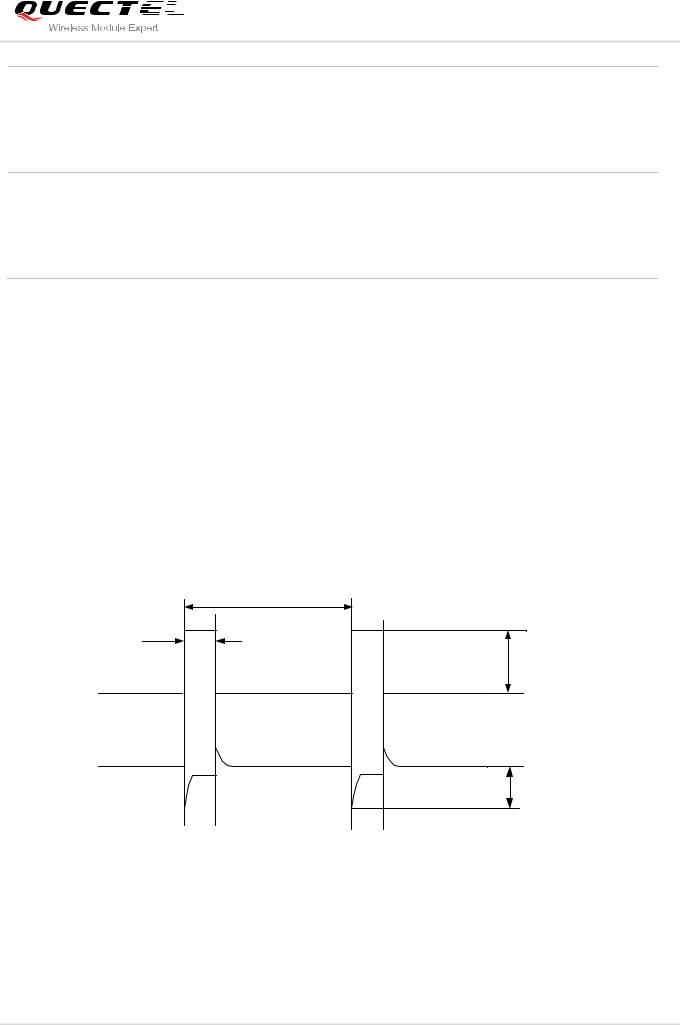
GSM/GPRS Module Series
M26 Hardware Design
Normal shutdown by sending the AT+QPOWD=1 command or using the PWRKEY pin. The power management ASIC disconnects the power supply from POWER DOWN the base band part of the module, and only the power supply for the RTC is remained. Software is not active. The UART interfaces are not accessible.
Operating voltage (connected to VBAT) remains applied.
Minimum
AT+CFUN command can set the module to a minimum functionality mode
Functionality Mode
without removing the power supply. In this case, the RF part of the module will not
(without removing
work or the SIM card will not be accessible, or both RF part and SIM card will be
power supply)
disabled, but the UART port is still accessible. The power consumption in this case is very low.
3.3. Power Supply
3.3.1. Power Features of Module
The power supply is one of the key issues in designing GSM terminals. Because of the 577us radio burst in GSM every 4.615ms, power supply must be able to deliver high current peaks in a burst period. During these peaks, drops on the supply voltage must not exceed minimum working voltage of module.
For the M26 module, the max current consumption could reach to 1.6A during a burst transmission. It will cause a large voltage drop on the VBAT. In order to ensure stable operation of the module, it is recommended that the max voltage drop during the burst transmission does not exceed 400mV.
4.615ms
577us
Burst:1.6A
IBAT
VBAT
Vdrop
Figure 3: Voltage Ripple during Transmitting
M26_Hardware_Design |
Confidential / Released |
22 / 80 |

GSM/GPRS Module Series
M26 Hardware Design
3.3.2. Decrease Supply Voltage Drop
The power supply range of the module is 3.3V to 4.6V. Make sure that the input voltage will never drop below 3.3V even in a burst transmission. If the power voltage drops below 3.3V, the module could turn off automatically. For better power performance, it is recommended to place a 100uF tantalum capacitor with low ESR (ESR=0.7Ω) and ceramic capacitor 100nF, 33pF and 10pF near the VBAT pin. The reference circuit is illustrated in Figure 4.
The VBAT route should be wide enough to ensure that there is not too much voltage drop during burst transmission. The width of trace should be no less than 2mm and the principle of the VBAT route is the longer route, the wider trace.
VBAT
+ |
|
|
|
|
|
|
|
|
|
|
|
|
|
|
|
|
|
C1 |
|
C2 |
C3 |
C4 |
|||||||||
|
|
|
|
|
|
|
|
|
|
|
|
|
|
|
|
|
|
|
|
|
|
|
|
|
|
|
|
|
|
|
|
|
|
|
|
|
|
|
|
|
|
|
|
|
|
|
|
|
|
|
|
|
|
|
|
|
|
|
|
|
|
|
|
|
|
|
100uF |
|
100nF |
10pF |
33pF |
||||||||
|
|
|
|
|
|
|
|
|
|
|
0603 |
|
0603 |
||
|
|
|
|
|
|
|
|
|
|
|
|
|
|
|
|
|
|
|
|
|
|
|
|
|
|
|
|
|
|
|
|
|
|
|
|
|
|
|
|
|
|
|
|
|
|
|
|
|
|
|
|
|
|
|
|
|
|
|
|
|
|
|
|
GND
Figure 4: Reference Circuit for the VBAT Input
3.3.3. Reference Design For Power Supply
The power design for the module is very important, since the performance of power supply for the module largely depends on the power source. The power supply is capable of providing the sufficient current up to 2A at least. If the voltage drop between the input and output is not too high, it is suggested to use a LDO as module’s power supply. If there is a big voltage difference between the input source and the desired output (VBAT), a switcher power converter is recommended to use as a power supply.
The following figure shows a reference design for +5V input power source. The designed output for the power supply is 4.0V and the maximum load current is 3A. In addition, in order to get a stable output voltage, a zener diode is placed close to the pins of VBAT. As to the zener diode, it is suggested to use a zener diode whose reverse zener voltage is 5.1V and dissipation power is more than 1 Watt.
M26_Hardware_Design |
Confidential / Released |
23 / 80 |
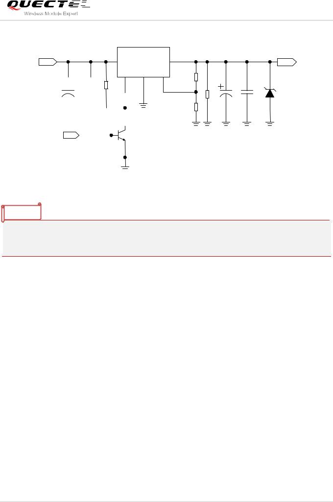
GSM/GPRS Module Series
M26 Hardware Design
MIC29302WU U1
DC_IN
2 IN
C1 |
|
|
C2 |
1 |
|
|
|||||||||||||||||||
|
|
|
|
|
|
|
|
|
|
|
|
|
|
|
|
|
|
|
|
R1 |
|
||||
|
|
|
|
|
|
|
|
|
|
|
|
|
|
|
|
|
|
|
|
|
|||||
|
|
|
|
|
|
|
|
|
|
|
|
|
|
|
|
|
|
|
|
|
|
||||
470uF |
|
|
100nF |
|
|
|
|
|
51K |
|
|||||||||||||||
|
|
|
|
|
|
|
|
|
|
|
|
|
|||||||||||||
|
|
|
|
|
|
|
|
|
|
|
|
|
|
|
|
|
|
|
|
||||||
|
|
|
|
|
|
|
|
|
|
|
|
|
|
|
|
|
R5 |
|
|||||||
|
|
|
|
|
|
|
|
|
|
|
|
|
|
|
|
|
|
||||||||
|
|
|
|
|
|
|
|
|
|
|
|
|
|
|
|
|
|
||||||||
|
|
|
|
|
|
|
|
|
|
|
|
|
|
|
|
|
|
||||||||
|
|
|
|
|
|
|
|
|
|
|
|
|
|
|
|
|
|
||||||||
|
|
|
|
|
|
|
|
|
|
|
|
|
|
|
|
4.7K |
|
||||||||
|
|
|
|
|
|
|
|
|
|
|
|
|
|
|
|
|
|
|
|
|
|
|
|
|
|
MCU_POWER_ON/OFF |
|
|
|
||||||||||||||||||||||
|
|
|
|
|
|
|
|
|
|
|
|
|
|
|
|
|
|
R6 |
|
|
|
|
|
||
|
|
|
|
|
|
|
|
|
|
|
|
|
|
|
|
|
|
47K |
|
|
|
|
|
||
|
|
|
|
|
|
|
|
|
|
|
|
|
|
|
|
|
|
|
|
|
|
|
|
|
|
|
|
|
|
|
|
|
|
|
|
|
|
|
|
|
|
|
|
|
|
|
|
|
|
|
|
|
|
|
|
|
|
|
VBAT |
|
|
OUT 4 |
|
|
|
|
|
|
|
|
R2 |
|
|
|
|
EN |
3 GND |
5 ADJ |
124K |
|
C3 |
C4 |
|
|
R4 |
D1 |
|||||
|
|
|
|
||||
|
|
|
R3 |
470R |
470uF |
100nF |
5.1V |
|
|
|
56K |
||||
|
|
|
|
|
|
|
Figure 5: Reference Circuit for Power Supply
NOTE
It is suggested to control the module’s main power supply (VBAT) via LDO enable pin to restart the module when the module has become abnormal. Power switch circuit like P-channel MOSFET switch circuit can also be used to control VBAT.
3.3.4. Monitor Power Supply
The command ―AT+CBC‖ can be used to monitor the supply voltage of the module. The unit of the displayed voltage is mV.
For details, please refer to the document [1].
3.4. Power On and Down Scenarios
3.4.1. Power On
The module can be turned on by driving the pin PWRKEY to a low level voltage. An open collector driver circuit is suggested to control the PWRKEY. A simple reference circuit is illustrated as below.
M26_Hardware_Design |
Confidential / Released |
24 / 80 |
 Loading...