

Page 1

BC66 Hardware Design
NB-IoT Module Series
Rev. BC66_Hardware_Design_V1.1
Date: 2018-11-14
Status: Released
www.quectel.com
Page 2

NB-IoT Module Series
BC66 Hardware Design
Our aim is to provide customers with timely and comprehensive service. For any
assistance, please contact our company headquarters:
Quectel Wireless Solutions Co., Ltd.
7th Floor, Hongye Building, No.1801 Hongmei Road, Xuhui District, Shanghai 200233, China
Tel: +86 21 5108 6236
Email: info@quectel.com
Or our local office. For more information, please visit:
http://www.quectel.com/support/sales.htm
For technical support, or to report documentation errors, please visit:
http://www.quectel.com/support/technical.htm
Or email to: support@quectel.com
GENERAL NOTES
QUECTEL OFFERS THE INFORMATION AS A SERVICE TO ITS CUSTOMERS. THE INFORMATION
PROVIDED IS BASED UPON CUSTOMERS’ REQUIREMENTS. QUECTEL MAKES EVERY EFFORT
TO ENSURE THE QUALITY OF THE INFORMATION IT MAKES AVAILABLE. QUECTEL DOES NOT
MAKE ANY WARRANTY AS TO THE INFORMATION CONTAINED HEREIN, AND DOES NOT ACCEPT
ANY LIABILITY FOR ANY INJURY, LOSS OR DAMAGE OF ANY KIND INCURRED BY USE OF OR
RELIANCE UPON THE INFORMATION. ALL INFORMATION SUPPLIED HEREIN IS SUBJECT TO
CHANGE WITHOUT PRIOR NOTICE.
COPYRIGHT
THE INFORMATION CONTAINED HERE IS PROPRIETARY TECHNICAL INFORMATION OF QUECTEL
WIRELESS SOLUTIONS CO., LTD. TRANSMITTING, REPRODUCTION, DISSEMINATION AND
EDITING OF THIS DOCUMENT AS WELL AS UTILIZATION OF THE CONTENT ARE FORBIDDEN
WITHOUT PERMISSION. OFFENDERS WILL BE HELD LIABLE FOR PAYMENT OF DAMAGES. ALL
RIGHTS ARE RESERVED IN THE EVENT OF A PATENT GRANT OR REGISTRATION OF A UTILITY
MODEL OR DESIGN.
Copyright © Quectel Wireless Solutions Co., Ltd. 2018. All rights reserved.
BC66_Hardware_Design 1 / 57
Page 3

NB-IoT Module Series
BC66 Hardware Design
About the Document
History
Revision Date Author Description
1.0 2018-08-24
1.1 2018-11-14 Newgate HUA
Speed SUN/
Newgate HUA
Initial
Updated supported bands and involved RF parameters of
BC66.
BC66_Hardware_Design 2 / 57
Page 4

NB-IoT Module Series
BC66 Hardware Design
Contents
About the Document ................................................................................................................................ 2
Contents .................................................................................................................................................... 3
Table Index ............................................................................................................................................... 5
Figure Index .............................................................................................................................................. 6
1 Introduction ....................................................................................................................................... 7
1.1. Safety Information .................................................................................................................... 8
2 Product Concept ............................................................................................................................... 9
2.1. General Description .................................................................................................................. 9
2.2. Key Features .......................................................................................................................... 10
2.3. Functional Diagram .................................................................................................................11
2.4. Development Board ................................................................................................................ 12
3 Application Interfaces ..................................................................................................................... 13
3.1. General Description ................................................................................................................ 13
3.2. Pin Assignment ....................................................................................................................... 14
3.3. Pin Description ....................................................................................................................... 15
3.4. Operating Modes .................................................................................................................... 18
3.5. Power Saving Mode (PSM) .................................................................................................... 19
3.6. Power Supply ......................................................................................................................... 20
3.6.1. Power Supply Pins ....................................................................................................... 20
3.6.2. Reference Design for Power Supply ............................................................................ 21
3.7. Power up/Power down Scenarios ........................................................................................... 21
3.7.1. Turn on ........................................................................................................................ 21
3.7.2. Turn off ........................................................................................................................ 23
3.7.3. Reset the Module ......................................................................................................... 24
3.8. UART Interfaces ..................................................................................................................... 25
3.8.1. Main UART Port ........................................................................................................... 26
3.8.2. Debug UART Port ........................................................................................................ 26
3.8.3. Auxiliary UART Port ..................................................................................................... 27
3.8.4. UART Application ......................................................................................................... 27
3.9. SPI Interface ........................................................................................................................... 29
3.10. USIM Interface ....................................................................................................................... 30
3.11. ADC Interface ......................................................................................................................... 32
3.12. RI Behaviors* ......................................................................................................................... 32
3.13. Network Status Indication* ...................................................................................................... 32
4
Antenna Interface ............................................................................................................................ 34
4.1. Pin Definition .......................................................................................................................... 34
4.2. Operating Frequencies ........................................................................................................... 34
4.3. RF Antenna Reference Design ............................................................................................... 35
4.4. Reference Design of RF Layout ............................................................................................. 36
BC66_Hardware_Design 3 / 57
Page 5

NB-IoT Module Series
BC66 Hardware Design
4.5. Antenna Requirements ........................................................................................................... 38
4.6. RF Output Power .................................................................................................................... 39
4.7. RF Receiving Sensitivity ......................................................................................................... 40
4.8. Recommended RF Connector for Antenna Installation ........................................................... 41
5 Electrical and Reliability Characteristics ...................................................................................... 43
5.1. Operation and Storage Temperatures ..................................................................................... 43
5.2. Current Consumption ............................................................................................................. 43
5.3. Electrostatic Discharge ........................................................................................................... 45
6 Mechanical Dimensions.................................................................................................................. 47
6.1. Mechanical Dimensions of the Module ................................................................................... 47
6.2. Recommended Footprint ........................................................................................................ 49
6.3. Top and Bottom Views of the Module ..................................................................................... 50
7 Storage, Manufacturing and Packaging ........................................................................................ 51
7.1. Storage ................................................................................................................................... 51
7.2. Manufacturing and Soldering .................................................................................................. 52
7.3. Packaging ............................................................................................................................... 53
7.3.1. Tape and Reel Packaging ............................................................................................ 53
8 Appendix A References .................................................................................................................. 55
BC66_Hardware_Design 4 / 57
Page 6

NB-IoT Module Series
BC66 Hardware Design
Table Index
TABLE 1: FREQUENCY BANDS OF BC66 MODULE ........................................................................................ 9
TABLE 2: BC66 KEY FEATURES ..................................................................................................................... 10
TABLE 3: I/O PARAMETERS DEFINITION ....................................................................................................... 15
TABLE 4: PIN DESCRIPTION ........................................................................................................................... 15
TABLE 5: OVERVIEW OF OPERATING MODES ............................................................................................. 18
TABLE 6: POWER SUPPLY PINS ..................................................................................................................... 20
TABLE 7: PWRKEY PIN .................................................................................................................................... 21
TABLE 8: RESET PIN ........................................................................................................................................ 24
TABLE 9: PIN DEFINITION OF UART INTERFACES ....................................................................................... 25
TABLE 10: PIN DEFINITION OF SPI INTERFACE ........................................................................................... 30
TABLE 11: PIN DEFINITION OF USIM INTERFACE ........................................................................................ 31
TABLE 12: PIN DEFINITION OF ADC INTERFACE ......................................................................................... 32
TABLE 13: PIN DEFINITION OF NB-IOT ANTENNA INTERFACE ................................................................... 34
TABLE 14: MODULE OPERATING FREQUENCIES ........................................................................................ 34
TABLE 15: ANTENNA CABLE INSERTION LOSS REQUIREMENTS ............................................................. 38
TABLE 16: REQUIRED ANTENNA PARAMETERS .......................................................................................... 38
TABLE 17: RF CONDUCTED OUTPUT POWER ............................................................................................. 39
TABLE 18: RECEIVING SENSITIVITY (WITH RF RETRANSMISSIONS) ....................................................... 40
TABLE 19: OPERATION AND STORAGE TEMPERATURES .......................................................................... 43
TABLE 20: MODULE CURRENT CONSUMPTION .......................................................................................... 44
TABLE 21: ELECTROSTATIC DISCHARGE CHARACTERISTICS (25ºC, 45% RELATIVE HUMIDITY) ........ 46
TABLE 22: RECOMMENDED THERMAL PROFILE PARAMETERS ............................................................... 52
TABLE 23: RELATED DOCUMENTS ................................................................................................................ 55
TABLE 24: TERMS AND ABBREVIATIONS ...................................................................................................... 55
BC66_Hardware_Design 5 / 57
Page 7

NB-IoT Module Series
BC66 Hardware Design
Figure Index
FIGURE 1: FUNCTIONAL DIAGRAM ............................................................................................................... 12
FIGURE 2: PIN ASSIGNMENT ......................................................................................................................... 14
FIGURE 3: MODULE POWER CONSUMPTION IN DIFFERENT MODES ...................................................... 19
FIGURE 4: TIMING OF WAKING UP MODULE FROM PSM ........................................................................... 20
FIGURE 5: REFERENCE CIRCUIT FOR POWER SUPPLY ............................................................................ 21
FIGURE 6: TURN ON THE MODULE USING DRIVING CIRCUIT ................................................................... 22
FIGURE 7: TURN ON THE MODULE USING KEYSTROKE ........................................................................... 22
FIGURE 8: POWER UP TIMING ....................................................................................................................... 22
FIGURE 9: POWER DOWN TIMING (POWER OFF BY AT COMMAND) ........................................................ 23
FIGURE 10: POWER DOWN TIMING (POWER OFF BY DISCONNECTING VBAT) ...................................... 23
FIGURE 11: REFERENCE CIRCUIT OF RESET BY USING DRIVING CIRCUIT ........................................... 24
FIGURE 12: REFERENCE CIRCUIT OF RESET BY USING BUTTON ........................................................... 24
FIGURE 13: RESET TIMING ............................................................................................................................. 25
FIGURE 14: REFERENCE DESIGN FOR MAIN UART PORT ........................................................................ 26
FIGURE 15: REFERENCE DESIGN OF DEBUG UART PORT ....................................................................... 27
FIGURE 16: REFERENCE DESIGN OF AUXILIARY UART PORT .................................................................. 27
FIGURE 17: REFERENCE CIRCUIT WITH VOLTAGE LEVEL TRANSLATOR CHIP ...................................... 28
FIGURE 18: REFERENCE CIRCUIT WITH TRANSISTOR CIRCUIT .............................................................. 28
FIGURE 19: SKETCH MAP FOR RS-232 INTERFACE MATCH ...................................................................... 29
FIGURE 20: SPI INTERFACE REFERENCE CIRCUIT WITH TRANSLATOR CHIP ....................................... 30
FIGURE 21: REFERENCE CIRCUIT FOR USIM INTERFACE WITH A 6-PIN USIM CARD CONNECTOR ... 31
FIGURE 22: REFERENCE DESIGN FOR NETLIGHT ..................................................................................... 33
FIGURE 23: REFERENCE DESIGN OF NB-IOT ANTENNA INTERFACE ...................................................... 36
FIGURE 24: MICROSTRIP LINE DESIGN ON A 2-LAYER PCB ...................................................................... 36
FIGURE 25: COPLANAR WAVEGUIDE LINE DESIGN ON A 2-LAYER PCB .................................................. 37
FIGURE 26: COPLANAR WAVEGUIDE LINE DESIGN ON A 4-LAYER PCB (LAYER 3 AS REFERENCE
GROUND) .................................................................................................................................................. 37
FIGURE 27: COPLANAR WAVEGUIDE LINE DESIGN ON A 4-LAYER PCB (LAYER 4 AS REFERENCE
GROUND) .................................................................................................................................................. 37
FIGURE 28: DIMENSIONS OF THE U.FL-R-SMT CONNECTOR (UNIT: MM) ................................................ 41
FIGURE 29: MECHANICALS OF U.FL-LP CONNECTORS ............................................................................. 41
FIGURE 30: SPACE FACTOR OF MATED CONNECTOR (UNIT: MM) ........................................................... 42
FIGURE 31: TOP VIEW OF THE MODULE ...................................................................................................... 50
FIGURE 32: BOTTOM VIEW OF THE MODULE .............................................................................................. 50
FIGURE 33: TAPE DIMENSIONS (UNIT: MM) .................................................................................................. 54
FIGURE 34: REEL DIMENSIONS (UNIT: MM) ................................................................................................. 54
BC66_Hardware_Design 6 / 57
Page 8

NB-IoT Module Series
BC66 Hardware Design
1 Introduction
This document defines the BC66 module and describes its air interface and hardware interface which are
connected with the customers’ applications.
This document can help customers quickly understand module interface specifications, electrical and
mechanical details, as well as other related information of the module. Associated with application notes
and user guides, customers can use BC66 to design and set up mobile applications easily.
BC66_Hardware_Design 7 / 57
Page 9
NB-IoT Module Series
BC66 Hardware Design
1.1. Safety Information
The following safety precautions must be observed during all phases of the operation, such as usage,
service or repair of any cellular terminal or mobile incorporating BC66 module. Manufacturers of the
cellular terminal should send the following safety information to users and operating personnel, and
incorporate these guidelines into all manuals supplied with the product. If not so, Quectel assumes no
liability for customers’ failure to comply with these precautions.
Full attention must be given to driving at all times in order to reduce the risk of an
accident. Using a mobile while driving (even with a handsfree kit) causes
distraction and can lead to an accident. Please comply with laws and regulations
restricting the use of wireless devices while driving.
Switch off the cellular terminal or mobile before boarding an aircraft. The operation
of wireless appliances in an aircraft is forbidden to prevent interference with
communication systems. If the device offers an Airplane Mode, then it should be
enabled prior to boarding an aircraft. Please consult the airline staff for more
restrictions on the use of wireless devices on boarding the aircraft.
Wireless devices may cause interference on sensitive medical equipment, so
please be aware of the restrictions on the use of wireless devices when in
hospitals, clinics or other healthcare facilities.
Cellular terminals or mobiles operating over radio signals and cellular network
cannot be guaranteed to connect in all possible conditions (for example, with
unpaid bills or with an invalid (U)SIM card). When emergent help is needed in such
conditions, please remember using emergency call. In order to make or receive a
call, the cellular terminal or mobile must be switched on in a service area with
adequate cellular signal strength.
The cellular terminal or mobile contains a transmitter and receiver. When it is ON, it
receives and transmits radio frequency signals. RF interference can occur if it is
used close to TV set, radio, computer or other electric equipment.
In locations with potentially explosive atmospheres, obey all posted signs to turn
off wireless devices such as your phone or other cellular terminals. Areas with
potentially explosive atmospheres include fuelling areas, below decks on boats,
fuel or chemical transfer or storage facilities, areas where the air contains
chemicals or particles such as grain, dust or metal powders, etc.
BC66_Hardware_Design 8 / 57
Page 10
NB-IoT Module Series
BC66 Hardware Design
2 Product Concept
2.1. General Description
BC66 is a high-performance NB-IoT module with extremely low power consumption. It is designed to
communicate with infrastructures of mobile network operators through NB-IoT radio protocols (3GPP
Rel.13 and 3GPP Rel.14*). BC66 supports a broad range of frequency bands as listed below.
Table 1: Frequency Bands of BC66 Module
Mode BC66
H-FDD B1/B2/B3/B4/B5/B8/B12/B13/B17/B18/B19/B20/B25/B26*/B28/B66
BC66 is an SMD type module with LCC package, and has an ultra-compact profile of 17.7mm × 15.8mm ×
2.0mm. These make it can be easily embedded into size-constrained applications and provide reliable
connectivity with the applications.
BC66 provides abundant external interfaces (UART, SPI*, ADC*, NETLIGHT*, etc.) and protocol stacks
(UDP/TCP, LwM2M, MQTT, etc.), which provide great convenience for customers' applications.
Due to compact form factor, ultra-low power consumption and extended temperature range, BC66 is a
best choice for a wide range of IoT applications, such as smart metering, bike sharing, smart wearables,
smart parking, smart city, home appliances, security and asset tracking, agricultural and environmental
monitoring, etc. It is able to provide a complete range of SMS* and data transmission services to meet
customers’ demands.
The module fully complies with the RoHS directive of the European Union.
NOTE
“*” means under development.
BC66_Hardware_Design 9 / 57
Page 11

NB-IoT Module Series
BC66 Hardware Design
2.2. Key Features
The following table describes the detailed features of BC66 module.
Table 2: BC66 Key Features
Feature Details
Power Supply
Power Saving
Frequency bands
Supply voltage: 2.1V ~ 3.63V
Typical supply voltage: 3.3V
Maximum power consumption: 5μA
Typical power consumption: 3.5μA
LTE Cat NB1:
B1/B2/B3/B4/B5/B8/B12/B13/B17/B18/B19/B20/B25/B26*/B28/B66
Transmitting Power 23dBm±2dB
USIM Interface Support 1.8V USIM card
Main UART Port:
Used for AT command communication and data transmission.
By default, the module is in auto-baud mode, and it supports automatic
baud rates not exceeding 115200bps. When powering on the module, the
MCU has to send AT command consecutively to synchronize baud rate
with the module. When OK is returned, it indicates the baud rate has been
synchronized successfully. When the module is woken up from PSM or
UART Interfaces
idle mode, the baud rate synchronized during start-up will be used directly.
Also can be used for firmware upgrade, and in such case, the baud rate is
921600bps by default.
Debug UART Port:
Used for firmware debugging
Default baud rate: 115200bps
Auxiliary UART Port:
Used for firmware debugging
Default baud rate: 115200bps
Network Protocols UDP/TCP/LwM2M/MQTT/CoAP*/PPP*/TLS*/DTLS*/HTTP*/HTTPS*
SMS* Text/PDU Mode
Data Transmission
Features
AT Commands
Single-tone: 25.5kbps (DL)/16.7kbps (UL)
Multi-tone: 25.5kbps (DL )/62.5kbps (UL)
3GPP TS 27.005/3GPP TS 27.007 AT commands (3GPP Rel. 13/Rel.14*)
and Quectel Enhanced AT commands
Firmware Update Upgrade firmware via main UART port or DFOTA
BC66_Hardware_Design 10 / 57
Page 12
NB-IoT Module Series
BC66 Hardware Design
Real Time Clock Supported
Physical
Characteristics
Temperature Range
Size: (17.7±0.15)mm × (15.8±0.15)mm × (2.0±0.2)mm
Weight: 1.2g±0.2g
1)
Operation temperature range: -35°C ~ +75°C
Extended temperature range: -40°C ~ +85°C
2)
Storage temperature range: -40°C ~ +90°C
Antenna Interface 50Ω impedance control
RoHS All hardware components are fully compliant with EU RoHS directive
NOTES
1)
1.
Within operation temperature range, the module is 3GPP compliant.
2)
2.
Within extended temperature range, the module remains the ability to establish and maintain an
SMS*, data transmission, etc. There is no unrecoverable malfunction. There are also no effects on
radio spectrum and no harm to radio network. Only one or more parameters like P
might reduce in
out
their value and exceed the specified tolerances. When the temperature returns to normal operation
temperature levels, the module will meet 3GPP specifications again.
3. "*" means under development.
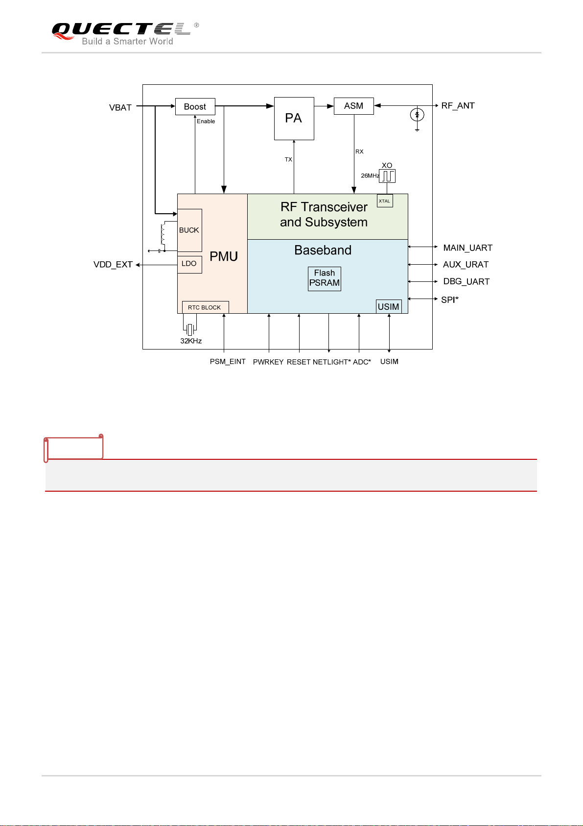
2.3. Functional Diagram
The following figure shows a block diagram of BC66 and illustrates the major functional parts.
Radio frequency
Baseband
Power management
Peripheral interfaces
BC66_Hardware_Design 11 / 57
Page 13
NB-IoT Module Series
BC66 Hardware Design
Figure 1: Functional Diagram
NOTE
“*” means under development.
2.4. Development Board
Quectel provides a complete set of development tools to facilitate the use and testing of BC66 module.
The development tool kit includes the TE-B board, USB cable, antenna and other peripherals. For more
details, please refer to document [1].
BC66_Hardware_Design 12 / 57
Page 14
NB-IoT Module Series
BC66 Hardware Design
3 Application Interfaces
3.1. General Description
BC66 is equipped with a total of 58 pins, including 44 LCC pins and 14 LGA pins. The subsequent
chapters will provide detailed descriptions of the following functions/pins/interfaces:
PSM
Power Supply
RESET
PWRKEY
UART Interfaces
SPI Interface
USIM Interface
ADC Interface
Network Status Indication*
Antenna Interface
NOTE
“*” means under development.
BC66_Hardware_Design 13 / 57
Page 15
NB-IoT Module Series
BC66 Hardware Design
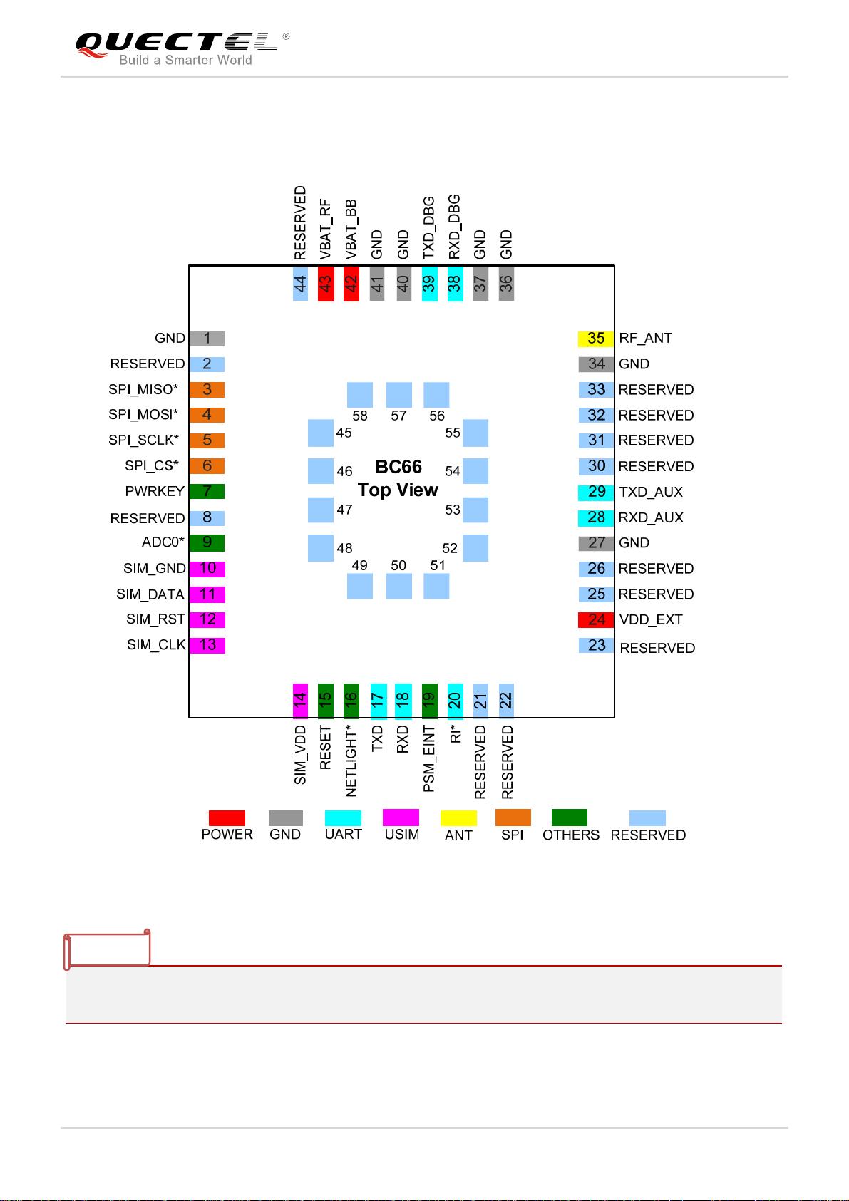
3.2. Pin Assignment
Figure 2: Pin Assignment
NOTES
1. Keep all reserved pins unconnected.
2. “*” means under development.
BC66_Hardware_Design 14 / 57
Page 16
NB-IoT Module Series
BC66 Hardware Design
3.3. Pin Description
Table 3: I/O Parameters Definition
Type Description
IO Bidirectional
DI Digital input
DO Digital output
PI Power input
PO Power output
AI Analog input
AO Analog output
Table 4: Pin Description
Power Supply
Pin Name Pin No. I/O Description DC Characteristics Comment
VBAT_BB 42 PI
VBAT_RF 43 PI
Power supply for
the module’s
baseband part
Power supply for
the module’s RF
part
Vmax=3.63V
Vmin=2.1V
Vnorm=3.3V
Vmax=3.63V
Vmin=2.1V
Vnorm=3.3V
No voltage output in
PSM mode.
It is intended to supply
VDD_
EXT
24 PO
1.8V output
power supply
Vnorm=1.8V
power for the module’s
pull-up circuits, and is
thus not recommended
to be used as the
power supply for
external circuits.
1, 27, 34,
GND
36, 37, 40,
GND
41
BC66_Hardware_Design 15 / 57
Page 17

NB-IoT Module Series
BC66 Hardware Design
Power Key Interface
Pin Name Pin No. I/O Description DC Characteristics Comment
PWRKEY 7 DI
Pull down
PWRKEY to turn
on the module
V
max=0.3*VBAT
IL
V
min=0.7*VBAT
IH
Reset Interface
Pin Name Pin No. I/O Description DC Characteristics Comment
RESET 15 DI Reset the module Active low.
PSM_EINT Interface
Pin Name Pin No. I/O Description DC Characteristics Comment
Dedicated
external interrupt
PSM_EINT 19 DI
pin.
Used to wake up
the module from
PSM.
Network Status Indication
Pin Name Pin No. I/O Description DC Characteristics Comment
NETLIGHT* 16 DO
Network status
indication
ADC Interface
Pin Name Pin No. I/O Description DC Characteristics Comment
General purpose
ADC0* 9 AI
analog to digital
converter
Voltage range:
0V~1.4V
interface
Main UART Port
Pin Name Pin No. I/O Description DC Characteristics Comment
RXD 18 DI Receive data
1.8V power domain.
TXD 17 DO Transmit data
Auxiliary UART Port
BC66_Hardware_Design 16 / 57
Page 18

NB-IoT Module Series
BC66 Hardware Design
Pin Name Pin No. I/O Description DC Characteristics Comment
RXD_AUX 28 DI Receive data
1.8V power domain.
TXD_AUX 29 DO Transmit data
Debug UART Port
Pin Name Pin No. I/O Description DC Characteristics Comment
RXD_DBG 38 DI Receive data
1.8V power domain.
TXD_DBG 39 DO Transmit data
Ringing Signal
Pin Name Pin No. I/O Description DC Characteristics Comment
RI* 20 DO Ring indicator 1.8V power domain.
USIM Interface
Pin Name Pin No. I/O Description DC Characteristics Comment
SIM_VDD 14 DO
SIM_RST 12 DO
SIM_DATA 11 IO
SIM_CLK 13 DO
USIM card
power supply
USIM card reset
signal
USIM card data
signal
USIM card clock
signal
Vnorm=1.8V
V
max=0.15×SIM_VDD
OL
V
min=0.85×SIM_VDD
OH
V
max=0.25×SIM_VDD
IL
VIHmin=0.75×SIM_VDD
max=0.15×SIM_VDD
V
OL
min=0.85×SIM_VDD
V
OH
V
max=0.15×SIM_VDD
OL
V
min=0.85×SIM_VDD
OH
Specified
SIM_GND 10 GND
ground for USIM
card
Antenna Interface
Pin Name Pin No. I/O Description DC Characteristics Comment
RF_ANT 35 IO
RF antenna
interface
50Ω characteristic
impedance
SPI Interface
Pin Name Pin No. I/O Description DC Characteristics Comment
BC66_Hardware_Design 17 / 57
Page 19
NB-IoT Module Series
BC66 Hardware Design
Master input
SPI_MISO* 3 DI
slave output of
SPI interface
Master output
SPI_MOSI* 4 DO
slave input of SPI
interface
1.8V power domain.
Serial clock
SPI_SCLK* 5 DO
signal of SPI
interface
SPI_CS* 6 DO
Chip select of
SPI interface
Reserved Pins
Pin Name Pin No. I/O Description DC Characteristics Comment
2, 8,
RESERVED
21~23,
25~26,
30~33,
Keep these pins
unconnected.
44~58
NOTES
1. Keep all unused pins unconnected.
2. “*” means under development.
3.4. Operating Modes
The following table briefly describes the three operating modes of the module.
Table 5: Overview of Operating Modes
Mode Function
In active mode, all functions of the module are available and all
Active
Normal Operation
Idle
BC66_Hardware_Design 18 / 57
processors are active; radio transmission and reception can be
performed. Transitions to idle mode or PSM can be initiated in active
mode.
In idle mode, the module is in light sleep and network connection is
maintained in DRX/eDRX state; paging messages can be received.
Transitions to active mode or PSM can be initiated in idle mode.
Page 20

NB-IoT Module Series
BC66 Hardware Design
In PSM, only the 32kHz RTC is working, and the network is
PSM
disconnected. The module will exit from PSM and enter into active
mode when the timer T3412 times out, and it can also be woken up
from PSM by PSM_EINT. For more details, please refer to Chapter 3.5.
3.5. Power Saving Mode (PSM)
Based on system performance, the module consumes an ultra-low current (maximally 5μA power
consumption) in PSM. PSM is designed to reduce power consumption of the module and improve battery
life. The following figure shows the power consumption of the module in different modes.
Figure 3: Module Power Consumption in Different Modes
The procedure for entering PSM is as follows: the module requests to enter PSM in “ATTACH REQUEST”
message during attach/TAU (Tracking Area Update) procedure. Then the network accepts the request
and provides an active time value (T3324) to the module and the mobile reachable timer starts. When the
T3324 timer expires, the module enters PSM for duration of T3412 (periodic TAU timer). Please note that
the module cannot request PSM when it is establishing an emergency attachment or initializing the PDN
(Public Data Network) connection.
When the module is in PSM, it cannot be paged and stops access stratum activities such as cell
reselection, but T3412 is still active.
Either of the following methods can make the module exit from PSM:
After the T3412 timer expires, the module will exit PSM automatically.
Pulling down PSM_EINT (falling edge) will wake the module up from PSM. The timing of waking up
the module from PSM is illustrated below.
BC66_Hardware_Design 19 / 57
Page 21

NB-IoT Module Series
BC66 Hardware Design
Figure 4: Timing of Waking up Module from PSM
NOTE
Among all GPIO interrupts, only the dedicated external interrupt pin PSM_EINT can successfully wake up
the module from PSM. The module cannot be woken up by any other general purpose GPIO interrupts.
3.6. Power Supply
3.6.1. Power Supply Pins
BC66 provides two VBAT pins for connection with an external power supply. The table below describes
the module's VBAT and ground pins.
Table 6: Power Supply Pins
Pin Name Pin No. Description Min. Typ. Max. Unit
Power supply for the
VBAT_BB 42
VBAT_RF 43
GND
1, 27, 34,
36, 37, 40, 41
module’s baseband
part
Power supply for the
module’s RF part
GND
2.1 3.3 3.63 V
2.1 3.3 3.63 V
BC66_Hardware_Design 20 / 57
Page 22
NB-IoT Module Series
BC66 Hardware Design
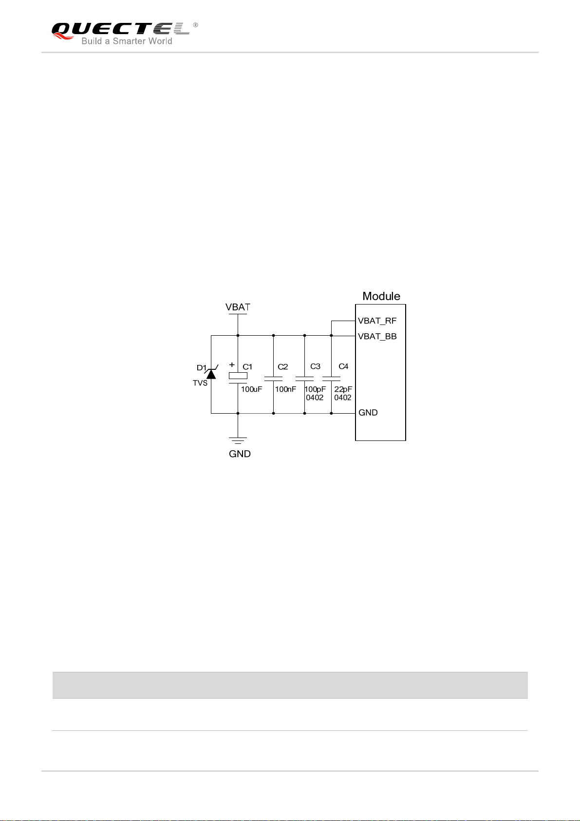
3.6.2. Reference Design for Power Supply
Power design for a module is critical to its performance. It is recommended to use a low quiescent current
LDO with output current capacity of 0.5A as the power supply for BC66. A Li-MnO2/2S alkaline battery
can also be used as the power supply. The supply voltage of the module ranges from 2.1V to 3.63V.
When the module is working, please make sure its input voltage will never drop below 2.1V; otherwise the
module will be abnormal.
For better power performance, it is recommended to place a 100uF tantalum capacitor with low ESR
(ESR=0.7Ω) and three ceramic capacitors (100nF, 100pF and 22pF) near the VBAT pins. Also, it is
recommended to add a TVS diode on the VBAT trace (near VBAT pins) to improve surge voltage
withstand capability. In principle, the longer the VBAT trace is, the wider it should be. A reference circuit
for power supply is illustrated in the following figure.
Figure 5: Reference Circuit for Power Supply
3.7. Power up/Power down Scenarios
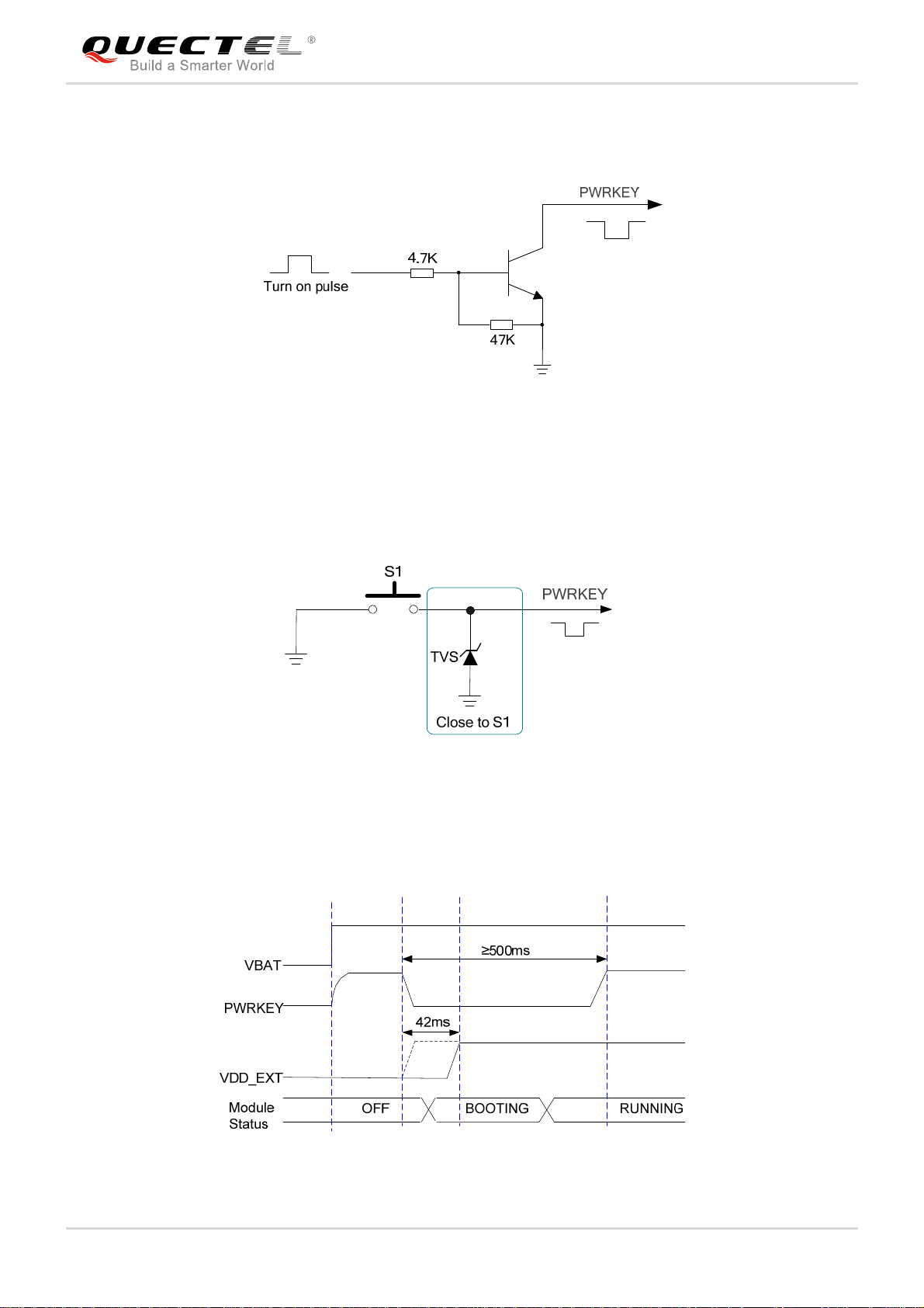
3.7.1. Turn on
BC66 will be powered up after driving the PWRKEY pin to a low level voltage for at least 500ms.
Table 7: PWRKEY Pin
Pin Name Pin No. Description PWRKEY Pull-down Time
PWRKEY 7
Pull down PWRKEY to power
up the module
≥500ms
BC66_Hardware_Design 21 / 57
Page 23
NB-IoT Module Series
BC66 Hardware Design
It is recommended use an open drain/collector driver to control the PWRKEY. A simple reference circuit is
illustrated in the following figure.
Figure 6: Turn on the Module Using Driving Circuit
Another way to control the PWRKEY is using a button directly. When pressing the key, electrostatic strike
may generate from the finger. Therefore, a TVS component is indispensable to be placed nearby the
button for ESD protection. A reference circuit is shown in the following figure.
Figure 7: Turn on the Module Using Keystroke
The power up timing is illustrated in the following figure.
Figure 8: Power up Timing
BC66_Hardware_Design 22 / 57
Page 24
NB-IoT Module Series
BC66 Hardware Design
NOTE
PWRKEY cannot be pulled down all the time, otherwise the module will not be able to enter into PSM.
3.7.2. Turn off
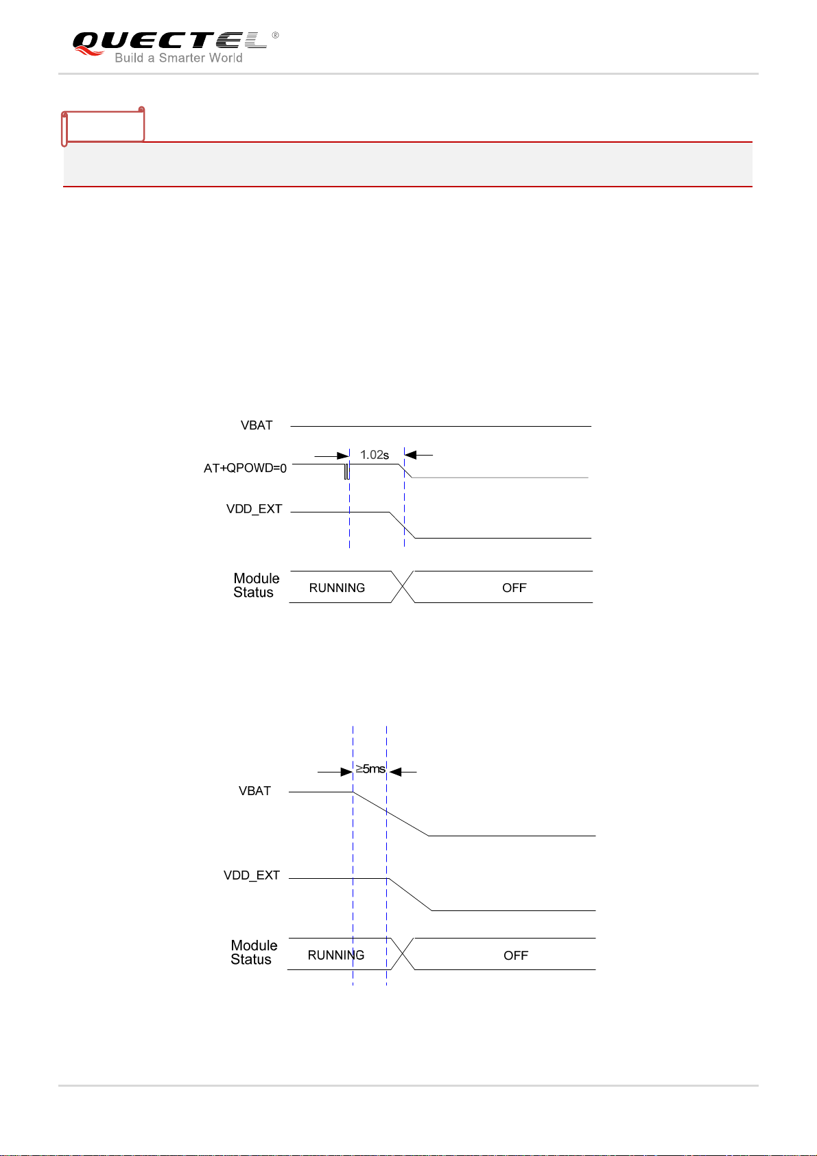
BC66 can be powered off though any of the following methods:
Power off by AT+QPOWD=0.
In emergent conditions, the module can be powered off through disconnecting VBAT power supply.
The module will be powered off automatically when VBAT drops below 2.1V.
Figure 9: Power down Timing (Power off by AT Command)
Figure 10: Power down Timing (Power off by Disconnecting VBAT)
BC66_Hardware_Design 23 / 57
Page 25
NB-IoT Module Series
BC66 Hardware Design
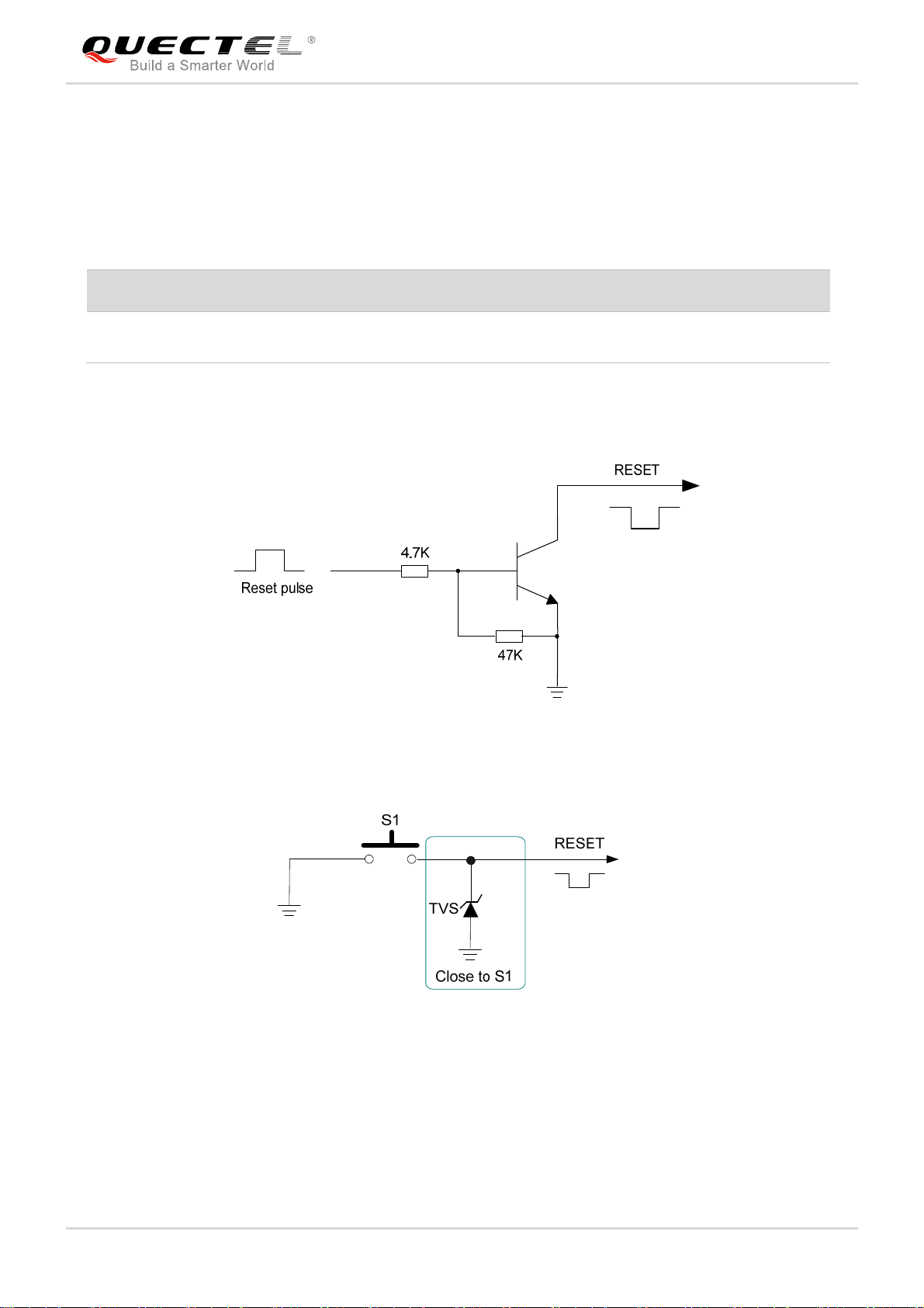
3.7.3. Reset the Module
Driving the RESET pin to a low level voltage for at least 50ms will reset the module.
Table 8: Reset Pin
Pin Name Pin No. Description Reset Pull-down Time
RESET 15
Reset the module.
Active low.
≥50ms
The recommended circuits of resetting the module are shown below. An open drain/collector driver or
button can be used to control the RESET pin.
Figure 11: Reference Circuit of RESET by Using Driving Circuit
Figure 12: Reference Circuit of RESET by Using Button
The reset scenario is illustrated in the following figure.
BC66_Hardware_Design 24 / 57
Page 26

NB-IoT Module Series
BC66 Hardware Design
Figure 13: Reset Timing
3.8. UART Interfaces
The module provides three UART ports: main UART port, debug UART port and auxiliary UART port. The
module is designed as DCE (Data Communication Equipment), following the traditional DCE-DTE (Data
Terminal Equipment) connection.
Table 9: Pin Definition of UART Interfaces
Interface Pin Name Pin No. Description Comment
TXD 17 Send data to RXD of DTE
Main UART Port
RXD 18 Receive data from TXD of DTE
RXD_DBG 38 Send data to RXD of DTE
Debug UART Port
TXD_DBG 39 Receive data from TXD of DTE
RXD_AUX 28 Send data to RXD of DTE
Auxiliary UART Port
TXD_AUX 29 Receive data from TXD of DTE
1.8V power
domain
Ring indicator (when there is a SMS
Ringing Signal RI* 20
or URC output, the module will inform
DTE with the RI* pin)
BC66_Hardware_Design 25 / 57
Page 27

NB-IoT Module Series
BC66 Hardware Design
NOTE
“*” means under development.
3.8.1. Main UART Port
The main UART port supports AT command communication, data transmission and firmware upgrade.
By default, the module is in auto-baud mode and it supports automatic baud rates not exceeding
115200bps. When powering on the module, the MCU has to send AT command consecutively to
synchronize baud rate with the module. When OK is returned, it indicates the baud rate has been
synchronized successfully. When the module is woken up from PSM or idle mode, the baud rate
synchronized during start-up will be used directly.
When the port is used for firmware upgrade, the baud rate is 921600bps by default.
The figure below shows the connection between DCE and DTE.
Figure 14: Reference Design for Main UART Port
3.8.2. Debug UART Port
Through debug tools, the debug UART port can be used to output logs for firmware debugging. Its baud
rate is 115200bps by default. The following is a reference design of debug UART port.
BC66_Hardware_Design 26 / 57
Page 28

NB-IoT Module Series
BC66 Hardware Design
Figure 15: Reference Design of Debug UART Port
3.8.3. Auxiliary UART Port
The auxiliary UART port is designed as a general purpose UART for communication with DTE. It also
supports log output for firmware debugging, and hardware flow control*. Its baud rate is 115200bps by
default. The following is a reference design of auxiliary UART port.
Figure 16: Reference Design of Auxiliary UART Port
3.8.4. UART Application
The module provides 1.8V UART interfaces. A level translator should be used if the application is
equipped with a 3.3V UART interface. A level translator TXS0108EPWR provided by Texas Instruments
(please visit http://www.ti.com
reference design.
for more information) is recommended. The following figure shows a
BC66_Hardware_Design 27 / 57
Page 29

NB-IoT Module Series
BC66 Hardware Design
Figure 17: Reference Circuit with Voltage Level Translator Chip
Another example with transistor translation circuit is shown as below. The circuit design of dotted line
section can refer to the design of solid line section, in terms of both module input and output circuit
designs, but please pay attention to the direction of connection.
Figure 18: Reference Circuit with Transistor Circuit
The following circuit shows a reference design for the communication between the module and a PC with
standard RS-232 interface. Please make sure the I/O voltage of level shifter which connects to module is
1.8V.
BC66_Hardware_Design 28 / 57
Page 30

NB-IoT Module Series
BC66 Hardware Design
Figure 19: Sketch Map for RS-232 Interface Match
Please visit vendors’ websites to select a suitable RS-232 transceiver, such as: http://www.exar.com
http://www.maximintegrated.com
.
and
NOTES
1. Transistor circuit solution is not suitable for applications with high baud rates exceeding 460Kbps.
2. “ ” represents the test point of UART interfaces. It is also recommended to reserve the test points of
VBAT and PWRKEY, for convenient firmware upgrade and debugging when necessary.
3. “*” means under development.
3.9. SPI Interface
BC66 provides one SPI master interface. The following table shows the pin definition of SPI interface.
BC66_Hardware_Design 29 / 57
Page 31

NB-IoT Module Series
BC66 Hardware Design
Table 10: Pin Definition of SPI Interface
Pin Name Pin No. I/O Description Comment
SPI_MISO 3 DI Master input slave output of SPI interface
SPI_MOSI 4 DO Master output slave input of SPI interface
1.8V power domain
SPI_SCLK 5 DO Clock signal of SPI interface
SPI_CS 6 DO Chip select of SPI interface
The module provides a 1.8V SPI interface. A level translator between the module and host should be
used if the application is equipped with a 3.3V processor or device interface. A voltage level translator that
supports SPI data rate is recommended. The following figure shows a reference design.
Figure 20: SPI Interface Reference Circuit with Translator Chip
3.10. USIM Interface
The module provides a USIM interface compliant to ISO/IEC 7816-3, enabling the module to access to an
external 1.8V USIM card.
The external USIM card is powered by an internal regulator in the module and supports 1.8V power
supply.
BC66_Hardware_Design 30 / 57
Page 32

NB-IoT Module Series
BC66 Hardware Design
Table 11: Pin Definition of USIM Interface
Pin Name Pin No. Description Comment
SIM_VDD 14 Power supply for USIM card
Voltage accuracy: 1.8V±5%.
Maximum supply current: about 60mA.
SIM_CLK 13 Clock signal of USIM card
SIM_DATA 11 Data signal of USIM card
SIM_RST 12 Reset signal of USIM card
SIM_GND 10 Specified ground for USIM card
A reference circuit design for USIM interface with a 6-pin USIM card connector is illustrated below.
Figure 21: Reference Circuit for USIM Interface with a 6-pin USIM Card Connector
For more information of USIM card connector, please visit http://www.amphenol.com
http://www.molex.com
.
or
In order to enhance the reliability and availability of USIM card in application, please follow the criteria
below in USIM circuit design:
Keep the placement of USIM card connector as close as possible to the module. Keep the trace
length as less than 200mm as possible.
Keep USIM card signals away from RF and VBAT traces.
Assure the trace between the ground of module and that of USIM card connector is short and wide.
Keep the trace width of ground no less than 0.5mm to maintain the same electric potential. The
decouple capacitor between SIM_VDD and GND should be not more than 1μF and be placed close
to the USIM card connector.
To avoid cross talk between SIM_DATA and SIM_CLK, keep them away from each other and shield
them separately with surrounded ground.
BC66_Hardware_Design 31 / 57
Page 33
NB-IoT Module Series
BC66 Hardware Design
In order to offer good ESD protection, it is recommended to add a TVS diode array. For more
information of TVS diode, please visit http://www.onsemi.com
placed as close to USIM card connector as possible, and make sure the USIM card signal lines go
through the ESD protection device first and then to the module. The 22Ω resistors should be
connected in series between the module and the USIM card connector so as to suppress EMI
spurious transmission and enhance ESD protection. Please note that the USIM peripheral circuit
should be close to the USIM card connector.
Place the RF bypass capacitors (33pF) close to the USIM card connector on all signal traces to
improve EMI suppression.
. The ESD protection device should be
3.11. ADC Interface
The module provides a 10-bit ADC input channel to read the voltage value. The interface is available in
both active and idle modes.
Table 12: Pin Definition of ADC Interface
Pin Name Pin No. Description
ADC0 9 Analog to digital converter interface
3.12. RI Behaviors*
When there is a SMS or URC output, the module will inform DTE with the RI pin. More details will be
added in the future version of this document.
NOTE
“*” means under development.
3.13. Network Status Indication*
The NETLIGHT signal can be used to drive a network status indicator LED.
A reference circuit is shown as below.
BC66_Hardware_Design 32 / 57
Page 34

NB-IoT Module Series
BC66 Hardware Design
Figure 22: Reference Design for NETLIGHT
NOTE
“*” means under development.
BC66_Hardware_Design 33 / 57
Page 35

NB-IoT Module Series
BC66 Hardware Design
4 Antenna Interface
The pin 35 is the RF antenna pad. The antenna port has an impedance of 50Ω.
4.1. Pin Definition
Table 13: Pin Definition of NB-IoT Antenna Interface
Pin Name Pin No. Description
RF_ANT 35 RF antenna interface
GND 34, 36, 37 Ground
4.2. Operating Frequencies
Table 14: Module Operating Frequencies
Frequency Band Receiving Frequency Transmitting Frequency
B1 2110MHz~2170MHz 1920MHz~1980MHz
B2 1930MHz~1990MHz 1850MHz~1910MHz
B3 1805MHz~1880MHz 1710MHz~1785MHz
B4 2110MHz~2155MHz 1710MHz~1755MHz
B5 869MHz~894MHz 824MHz~849MHz
B8 925MHz~960MHz 880MHz~915 MHz
B12 729MHz~746MHz 699MHz~716MHz
BC66_Hardware_Design 34 / 57
Page 36
NB-IoT Module Series
BC66 Hardware Design
B13 746MHz~756MHz 777MHz~787MHz
B17 734MHz~746MHz 704MHz~716MHz
B18 860MHz~875MHz 815MHz~830MHz
B19 875MHz~890MHz 830MHz~845MHz
B20 791MHz~821MHz 832MHz~862MHz
B25 1930MHz~1995MHz 1850MHz~1915MHz
B26* 859MHz~894MHz 814MHz~849MHz
B28 758MHz~803MHz 703MHz~748MHz
B66 2110MHz~2200MHz 1710MHz~1780MHz
NOTE
“*” means under development.
4.3. RF Antenna Reference Design
BC66 provides an RF antenna pad for external NB-IoT antenna connection.
The RF trace on host PCB connected to the module’s RF antenna pad should be coplanar
waveguide or microstrip, whose characteristic impedance should be close to 50Ω.
BC66 comes with ground pads which are next to the antenna pad in order to give a better grounding.
In order to achieve better RF performance, it is recommended to reserve a π type matching circuit
and place the π-type matching components (R1/C1/C2) as close to the antenna as possible. By
default, the capacitors (C1/C2) are not mounted and a 0Ω resistor is mounted on R1.
BC66_Hardware_Design 35 / 57
Page 37

NB-IoT Module Series
BC66 Hardware Design
A reference design of the RF interface is shown as below.
Figure 23: Reference Design of NB-IoT Antenna Interface
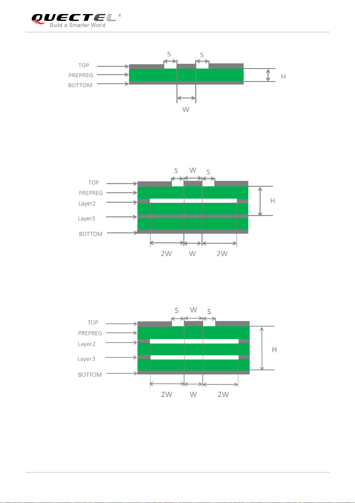
4.4. Reference Design of RF Layout
For user’s PCB, the characteristic impedance of all RF traces should be controlled as 50Ω. The
impedance of the RF traces is usually determined by the trace width (W), the materials’ dielectric constant,
the height between signal layer and reference ground (H), and the clearance between RF trace and
ground (S). Microstrip line or coplanar waveguide line is typically used in RF layout for characteristic
impedance control. The following are reference designs of microstrip line or coplanar waveguide line with
different PCB structures.
.
Figure 24: Microstrip Line Design on a 2-layer PCB
BC66_Hardware_Design 36 / 57
Page 38
NB-IoT Module Series
BC66 Hardware Design
Figure 25: Coplanar Waveguide Line Design on a 2-layer PCB
Figure 26: Coplanar Waveguide Line Design on a 4-layer PCB (Layer 3 as Reference Ground)
Figure 27: Coplanar Waveguide Line Design on a 4-layer PCB (Layer 4 as Reference Ground)
In order to ensure RF performance and reliability, the following principles should be complied with in RF
layout design:
BC66_Hardware_Design 37 / 57
Page 39

NB-IoT Module Series
BC66 Hardware Design
Use impedance simulation tool to control the characteristic impedance of RF traces as 50Ω.
The GND pins adjacent to RF pins should not be designed as thermal relief pads, and should be fully
connected to ground.
The distance between the RF pins and the RF connector should be as short as possible, and all the
right angle traces should be changed to curved ones.
There should be clearance area under the signal pin of the antenna connector or solder joint.
The reference ground of RF traces should be complete. Meanwhile, adding some ground vias around
RF traces and the reference ground could help to improve RF performance. The distance between
the ground vias and RF traces should be no less than two times the width of RF signal traces (2*W).
For more details, please refer to document [2].
4.5. Antenna Requirements
To minimize the loss on RF trace and RF cable, please pay attention to the antenna design. The following
tables show the requirements on NB-IoT antenna.
Table 15: Antenna Cable Insertion Loss Requirements
Band Requirements
LTE B5/B8/B12/B13/B17/B18/B19/B20/B26*/B28 Cable Insertion loss: <1dB
LTE B1/B2/B3/B4/B25/B66 Cable Insertion loss: <1.5dB
NOTE
“*” means under development.
Table 16: Required Antenna Parameters
Parameters Requirements
Frequency Range 699MHz~2200MHz
VSWR ≤2
Efficiency > 30%
Max Input Power (W) 50
BC66_Hardware_Design 38 / 57
Page 40

NB-IoT Module Series
BC66 Hardware Design
Input Impedance (Ω) 50
4.6. RF Output Power
Table 17: RF Conducted Output Power
Frequency Band Max. Min.
B1 23dBm±2dB <-39dBm
B2 23dBm±2dB <-39dBm
B3 23dBm±2dB <-39dBm
B4 23dBm±2dB <-39dBm
B5 23dBm±2dB <-39dBm
B8 23dBm±2dB <-39dBm
B12 23dBm±2dB <-39dBm
B13 23dBm±2dB <-39dBm
B17 23dBm±2dB <-39dBm
B18 23dBm±2dB <-39dBm
B19 23dBm±2dB <-39dBm
B20 23dBm±2dB <-39dBm
B25 23dBm±2dB <-39dBm
B26* TBD TBD
B28 23dBm±2dB <-39dBm
B66 23dBm±2dB <-39dBm
NOTES
1. The design conforms to the NB-IoT radio protocols in 3GPP Rel.13 and 3GPP Rel.14.
2. “*” means under development.
BC66_Hardware_Design 39 / 57
Page 41

NB-IoT Module Series
BC66 Hardware Design
4.7. RF Receiving Sensitivity
Table 18: Receiving Sensitivity (with RF Retransmissions)
Frequency Band Receiving Sensitivity
B1 -129dBm
B2 -129dBm
B3 -129dBm
B4 -129dBm
B5 -129dBm
B8 -129dBm
B12 -129dBm
B13 -129dBm
B17 -129dBm
B18 -129dBm
B19 -129dBm
B20 -129dBm
B25 -129dBm
B26* TBD
B28 -129dBm
B66 -129dBm
NOTE
“*” means under development.
BC66_Hardware_Design 40 / 57
Page 42

NB-IoT Module Series
BC66 Hardware Design
4.8. Recommended RF Connector for Antenna Installation
If RF connector is used for antenna connection, it is recommended to use the U.FL-R-SMT connector
provided by HIROSE.
Figure 28: Dimensions of the U.FL-R-SMT Connector (Unit: mm)
U.FL-LP serial connectors listed in the following figure can be used to match the U.FL-R-SMT.
Figure 29: Mechanicals of U.FL-LP Connectors
BC66_Hardware_Design 41 / 57
Page 43

NB-IoT Module Series
BC66 Hardware Design
The following figure describes the space factor of mated connector.
Figure 30: Space Factor of Mated Connector (Unit: mm)
For more details, please visit http://www.hirose.com
.
BC66_Hardware_Design 42 / 57
Page 44

NB-IoT Module Series
BC66 Hardware Design
5 Electrical and Reliability
Characteristics
5.1. Operation and Storage Temperatures
The following table lists the operation and storage temperatures of BC66.
Table 19: Operation and Storage Temperatures
Parameter Min. Typ. Max. Unit
Operation Temperature Range 1) -35 +25 +75 ºC
Extended Temperature Range 2) -40 +85 ºC
Storage Temperature Range -40 +90 ºC
NOTES
1)
1.
Within operation temperature range, the module is 3GPP compliant.
2)
2.
Within extended temperature range, the module remains the ability to establish and maintain an
SMS*, data transmission, etc. There is no unrecoverable malfunction. There are also no effects on
radio spectrum and no harm to radio network. Only one or more parameters like P
their value and exceed the specified tolerances. When the temperature returns to normal operation
temperature levels, the module will meet 3GPP specifications again.
might reduce in
out
5.2. Current Consumption
The table below lists the current consumption of BC66 under different states.
BC66_Hardware_Design 43 / 57
Page 45

NB-IoT Module Series
BC66 Hardware Design
Table 20: Module Current Consumption
Parameter Mode Description Min. Typ. Max. Unit
PSM Sleep mode 3.5 5 μA
eDRX=81.92s, PTW=40.96s 288 µA
I
VBAT
Idle
@DRX=1.28s 541 μA
@DRX=2.56s 434 μA
B1 @23dBm 100 285 mA
B2 @23dBm 103 294 mA
B3 @23dBm 107 308 mA
B4 @23dBm TBD TBD mA
B5 @23dBm 107 303 mA
B8 @23dBm 113 325 mA
B12 @23dBm 134 393 mA
Single-tone
B13 @23dBm 111 319 mA
(15kHz subcarrier
spacing)
B17 @23dBm 133 392 mA
Active 1)
Single-tone
(3.75kHz subcarrier
spacing)
B18 @23dBm 110 316 mA
B19 @23dBm 109 311 mA
B20 @23dBm 109 301 mA
B25 @23dBm 103 293 mA
B26* @23dBm TBD TBD mA
B28 @23dBm 128 375 mA
B66 @23dBm 109 312 mA
B1 @23dBm 193 302 mA
B2 @23dBm 187 296 mA
B3 @23dBm 215 335 mA
BC66_Hardware_Design 44 / 57
Page 46

NB-IoT Module Series
BC66 Hardware Design
Parameter Mode Description Min. Typ. Max. Unit
B4 @23dBm TBD TBD mA
B5 @23dBm 215 330 mA
B8 @23dBm 224 344 mA
B12 @23dBm 250 395 mA
B13 @23dBm 203 316 mA
B17 @23dBm 258 409 mA
B18 @23dBm 198 313 mA
B19 @23dBm 198 314 mA
B20 @23dBm 215 329 mA
B25 @23dBm 187 297 mA
B26* @23dBm TBD TBD mA
B28 @23dBm 250 398 mA
B66 @23dBm 200 316 mA
NOTES
1)
1.
Current consumption under instrument test condition.
2. “*” means under development.
5.3. Electrostatic Discharge
The module is not protected against electrostatics discharge (ESD) in general. Consequently, it is subject
to ESD handling precautions that typically apply to ESD sensitive components. Proper ESD handling and
packaging procedures must be applied throughout the processing, handling and operation of any
application that incorporates the module.
The following table shows the module’s electrostatic discharge characteristics.
BC66_Hardware_Design 45 / 57
Page 47

NB-IoT Module Series
BC66 Hardware Design
Table 21: Electrostatic Discharge Characteristics (25ºC, 45% Relative Humidity)
Test Contact Discharge Air Discharge Unit
VBAT, GND ±5 ±10 kV
Antenna interface ±5 ±10 kV
Other interfaces ±0.5 ±1 kV
BC66_Hardware_Design 46 / 57
Page 48

NB-IoT Module Series
BC66 Hardware Design
6 Mechanical Dimensions
This chapter describes the mechanical dimensions of the module. All dimensions are measured in
millimetre (mm), and the tolerances for dimensions without tolerance values are ±0.05mm.
6.1. Mechanical Dimensions of the Module
Figure 31: BC66 Top and Side Dimensions (Unit: mm)
BC66_Hardware_Design 47 / 57
Page 49
NB-IoT Module Series
BC66 Hardware Design
Figure 32: Module Bottom Dimension (Bottom View)
BC66_Hardware_Design 48 / 57
Page 50

NB-IoT Module Series
BC66 Hardware Design
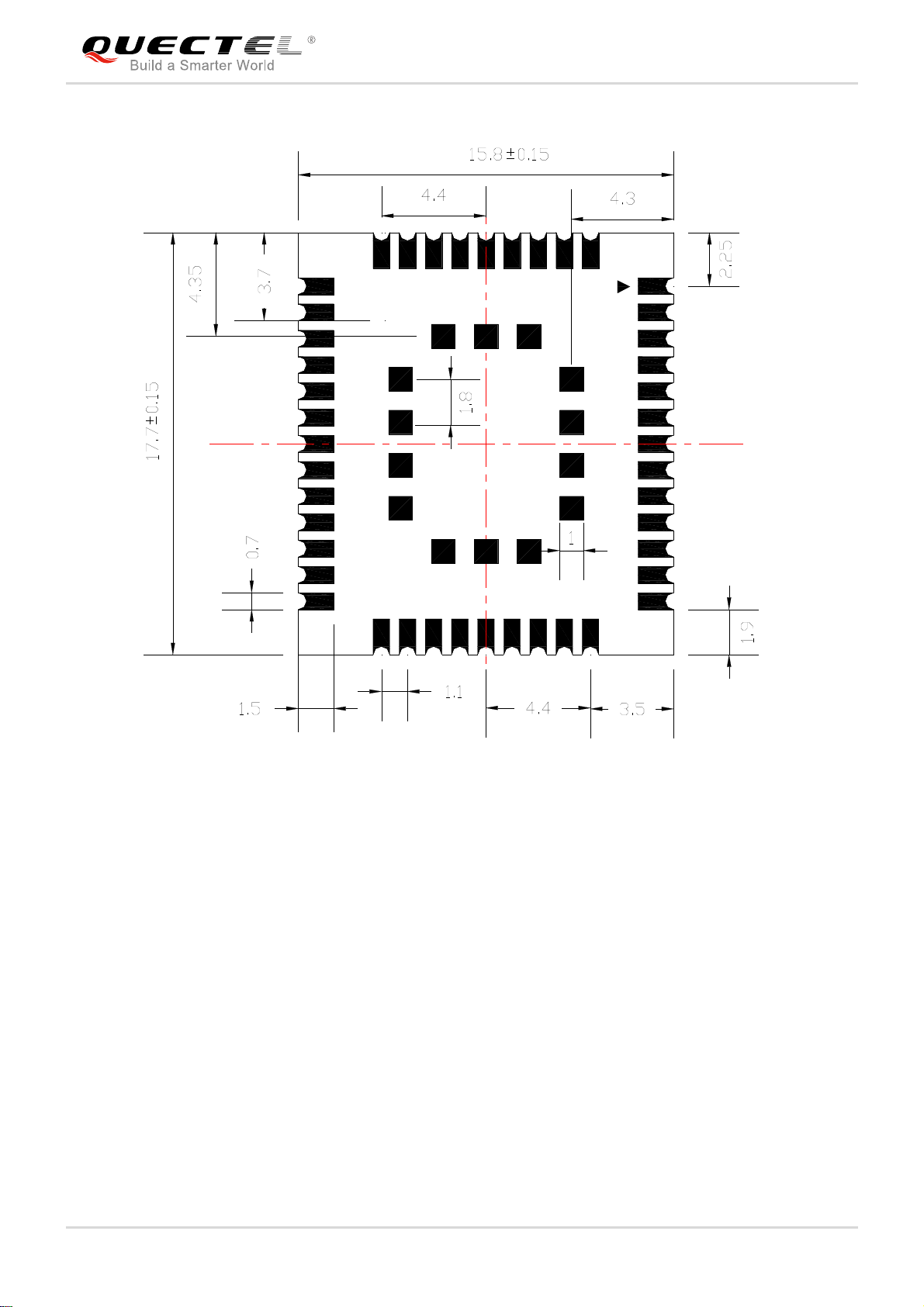
6.2. Recommended Footprint
36
1
23
14
Figure 33: Recommended Footprint (Unit: mm)
NOTE
The module should be kept about 3mm away from other components on the host PCB.
BC66_Hardware_Design 49 / 57
Page 51
NB-IoT Module Series
BC66 Hardware Design
6.3. Top and Bottom Views of the Module
Figure 31: Top View of the Module
Figure 32: Bottom View of the Module
NOTE
These are renderings of BC66 module. For authentic dimension and appearance, please refer to the
module that you receive from Quectel.
BC66_Hardware_Design 50 / 57
Page 52

NB-IoT Module Series
BC66 Hardware Design
7 Storage, Manufacturing and
Packaging
7.1. Storage
BC66 module is stored in a vacuum-sealed bag. It is rated at MSL 3, and storage restrictions are shown
as below.
1. Shelf life in the vacuum-sealed bag: 12 months at <40ºC/90%RH.
2. After the vacuum-sealed bag is opened, devices that will be subjected to reflow soldering or other
high temperature processes must be:
Mounted within 168 hours at the factory environment of ≤30ºC/60%RH.
Stored at <10%RH.
3. Devices require baking before mounting, if any circumstance below occurs.
When the ambient temperature is 23ºC±5ºC and the humidity indication card shows the humidity
is >10% before opening the vacuum-sealed bag.
Device mounting cannot be finished within 168 hours at factory conditions of ≤30ºC/60%.
4. If baking is required, devices may be baked for 8 hours at 120ºC±5ºC.
NOTE
As the plastic package cannot be subjected to high temperature, it should be removed from devices
before high temperature (120ºC) baking. If shorter baking time is desired, please refer to
IPC/JEDECJ-STD-033 for baking procedure.
BC66_Hardware_Design 51 / 57
Page 53
NB-IoT Module Series
BC66 Hardware Design
7.2. Manufacturing and Soldering
Push the squeegee to apply the solder paste on the surface of stencil, thus making the paste fill the
stencil openings and then penetrate to the PCB. The force on the squeegee should be adjusted properly
so as to produce a clean stencil surface on a single pass. To ensure the module soldering quality, the
thickness of stencil for the module is recommended to be 0.15mm~0.18mm. For more details, please
refer to document [4].
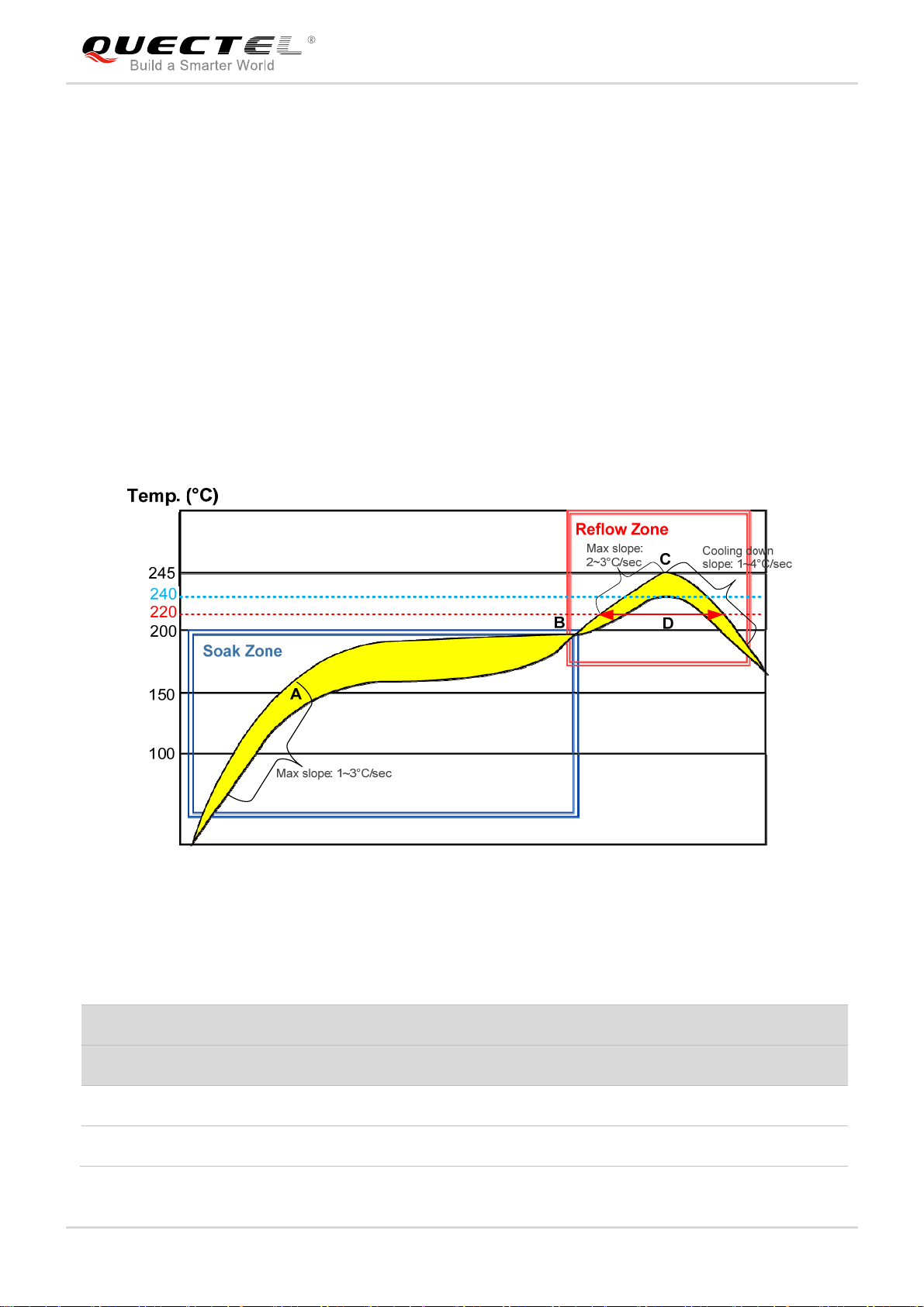
It is suggested that the peak reflow temperature is 240~245ºC, and the absolute maximum reflow
temperature is 245ºC. To avoid damage to the module caused by repeated heating, it is strongly
recommended that the module should be mounted after reflow soldering for the other side of PCB has
been completed. The recommended reflow soldering thermal profile (lead-free reflow soldering) and
related parameters are shown below.
Figure 36: Recommended Reflow Soldering Thermal Profile
Table 22: Recommended Thermal Profile Parameters
Factor Recommendation
Soak Zone
Max slope 1 to 3°C/sec
Soak time (between A and B: 150°C and 200°C) 60 to 120 sec
BC66_Hardware_Design 52 / 57
Page 54
NB-IoT Module Series
BC66 Hardware Design
Reflow Zone
Max slope 2 to 3°C/sec
Reflow time (D: over 220°C) 40 to 60 sec
Max temperature 240°C ~ 245°C
Cooling down slope 1 to 4°C/sec
Reflow Cycle
Max reflow cycle 1
NOTES
1. During manufacturing and soldering, or any other processes that may contact the module directly,
NEVER wipe the module’s shielding can with organic solvents, such as acetone, ethyl alcohol,
isopropyl alcohol, trichloroethylene, etc. Otherwise, the shielding can may become rusted.
2. The shielding can for the module is made of Cupro-Nickel base material. It is tested that after 12
hours’ Neutral Salt Spray test, the laser engraved label information on the shielding can is still clearly
identifiable and the QR code is still readable, although white rust may be found.
7.3. Packaging
The modules are stored in a vacuum-sealed bag which is ESD protected. The bag should not be opened
until the devices are ready to be soldered onto the application.
7.3.1. Tape and Reel Packaging
The reel is 330mm in diameter and each reel contains 250 modules.
BC66_Hardware_Design 53 / 57
Page 55

NB-IoT Module Series
BC66 Hardware Design
Figure 33: Tape Dimensions (Unit: mm)
Figure 34: Reel Dimensions (Unit: mm)
BC66_Hardware_Design 54 / 57
Page 56
NB-IoT Module Series
BC66 Hardware Design
8 Appendix A References
Table 23: Related Documents
SN Document Name Remark
[1] Quectel_BC66-TE-B_User_Guide BC66-TE-B User Guide
[2] Quectel_RF_Layout_Application_Note RF Layout Application Note
[3] Quectel_BC66_AT_Commands_Manual BC66 AT Commands Manual
[4] Quectel_Module_Secondary_SMT_User_Guide Module Secondary SMT User Guide
Table 24: Terms and Abbreviations
Abbreviation Description
ADC Analog-to-Digital Converter
CoAP Constrained Application Protocol
DCE Data Communications Equipment (typically module)
DTE Data Terminal Equipment (typically computer, external controller)
DTLS Datagram Transport Layer Security
EMI Electromagnetic Interference
ESD Electrostatic Discharge
FTP File Transfer Protocol
H-FDD Half Frequency Division Duplexing
HTTP Hyper Text Transfer Protocol
HTTPS Hyper Text Transfer Protocol over Secure Socket Layer
I/O Input/Output
BC66_Hardware_Design 55 / 57
Page 57

NB-IoT Module Series
BC66 Hardware Design
kbps Kilo Bits Per Second
LED Light Emitting Diode
Li-MnO2 Lithium-manganese Dioxide
Li-2S Lithium Sulfur
LTE Long Term Evolution
LwM2M Lightweight M2M
MQTT Message Queuing Telemetry Transport
NB-IoT Narrow Band- Internet of Things
PCB Printed Circuit Board
PDU Protocol Data Unit
PPP Point-to-Point Protocol
PSM Power Save Mode
RF Radio Frequency
RTC Real Time Clock
RXD Receive Data
SMS Short Message Service
SSL Secure Sockets Layer
TCP Transmission Control Protocol
TE Terminal Equipment
TXD Transmitting Data
UART Universal Asynchronous Receiver & Transmitter
UDP User Datagram Protocol
URC Unsolicited Result Code
USIM Universal Subscriber Identification Module
VSWR Voltage Standing Wave Ratio
BC66_Hardware_Design 56 / 57
Page 58

NB-IoT Module Series
BC66 Hardware Design
Vmax Maximum Voltage Value
Vnorm Normal Voltage Value
Vmin Minimum Voltage Value
VIHmax Maximum Input High Level Voltage Value
VIHmin Minimum Input High Level Voltage Value
VILmax Maximum Input Low Level Voltage Value
VILmin Minimum Input Low Level Voltage Value
VImax Absolute Maximum Input Voltage Value
VInorm Absolute Normal Input Voltage Value
VImin Absolute Minimum Input Voltage Value
VOHmax Maximum Output High Level Voltage Value
VOHmin Minimum Output High Level Voltage Value
VOLmax Maximum Output Low Level Voltage Value
VOLmin Minimum Output Low Level Voltage Value
BC66_Hardware_Design 57 / 57
Page 59

NB-IoT Module Series
BC66 Hardware Design
FCC Certification Requirements.
According to the definition of mobile and fixed device is described in Part 2.1091(b), this device is a
mobile device.
And the following conditions must be met:
1. This Modular Approval is limited to OEM installation for mobile and fixed applications only. The antenna
installation and operating configurations of this transmitter, including any applicable source-based time-
averaging duty factor, antenna gain and cable loss must satisfy MPE categorical Exclusion Requirements
of 2.1091.
2. The EUT is a mobile device; maintain at least a 20 cm separation between the EUT and the user’s body
and must not transmit simultaneously with any other antenna or transmitter.
3.A label with the following statements must be attached to the host end product: This device contains
FCC ID: XMR201808BC66.
4.To comply with FCC regulations limiting both maximum RF output power and human exposure to RF
radiation, maximum antenna gain (including cable loss) must not exceed:
❒ LTE Band2/25:≤8dBi
❒ LTE Band4/66:≤4dBi
❒ LTE Band5:≤9.42dBi
❒ LTE Band12:≤8.73dBi
❒ LTE Band13:≤9.17dBi
❒ LTE Band17:≤8.73dBi
5. This module must not transmit simultaneously with any other antenna or transmitter
6. The host end product must include a user manual that clearly defines operating requirements and
conditions that must be observed to ensure compliance with current FCC RF exposure guidelines.
For portable devices, in addition to the conditions 3 through 6 described above, a separate approval is
required to satisfy the SAR requirements of FCC Part 2.1093
BC66_Hardware_Design 58 / 57
Page 60

NB-IoT Module Series
BC66 Hardware Design
If the device is used for other equipment that separate approval is required for all other operating
configurations, including portable configurations with respect to 2.1093 and different antenna
configurations.
For this device, OEM integrators must be provided with labeling instructions of finished products.
Please refer to KDB784748 D01 v07, section 8. Page 6/7 last two paragraphs:
A certified modular has the option to use a permanently affixed label, or an electronic label. For a
permanently affixed label, the module must be labeled with an FCC ID - Section 2.926 (see 2.2
Certification (labeling requirements) above). The OEM manual must provide clear instructions
explaining to the OEM the labeling requirements, options and OEM user manual instructions that are
required (see next paragraph).
For a host using a certified modular with a standard fixed label, if (1) the module’s FCC ID is not visible
when installed in the host, or (2) if the host is marketed so that end users do not have straightforward
commonly used methods for access to remove the module so that the FCC ID of the module is visible;
then an additional permanent label referring to the enclosed module:“Contains Transmitter Module FCC
ID: XMR201808BC66” or “Contains FCC ID: XMR201808BC66” must be used. The host OEM user
manual must also contain clear instructions on how end users can find and/or access the module and
the FCC ID.
The final host / module combination may also need to be evaluated against the FCC Part 15B criteria
for unintentional radiators in order to be properly authorized for operation as a Part 15 digital device.
The user’s manual or instruction manual for an intentional or unintentional radiator shall caution the
user that changes or modifications not expressly approved by the party responsible for compliance
could void the user's authority to operate the equipment. In cases where the manual is provided only in
a form other than paper, such as on a computer disk or over the Internet, the information required by
this section may be included in the manual in that alternative form, provided the user can reasonably be
expected to have the capability to access information in that form.
This device complies with part 15 of the FCC Rules. Operation is subject to the following two conditions:
BC66_Hardware_Design 59 / 57
Page 61

NB-IoT Module Series
BC66 Hardware Design
(1) This device may not cause harmful interference, and (2) this device must accept any interference
received, including interference that may cause undesired operation.
Changes or modifications not expressly approved by the manufacturer could void the user’s authority to
operate the equipment.
To ensure compliance with all non-transmitter functions the host manufacturer is responsible for ensuring
compliance with the module(s) installed and fully operational. For example, if a host was previously
authorized as an unintentional radiator under the Supplier’s Declaration of Conformity procedure without
a transmitter certified module and a module is added, the host manufacturer is responsible for ensuring
that the after the module is installed and operational the host continues to be compliant with the Part 15B
unintentional radiator requirements.
IC Statement
IRSS-GEN
"This device complies with Industry Canada’s licence-exempt RSSs. Operation is subject to the following
two conditions: (1) This device may not cause interference; and (2) This device must accept any
interference, including interference that may cause undesired operation of the device." or "Le présent
appareil est conforme aux CNR d’Industrie Canada applicables aux appareils radio exempts de licence.
L’exploitation est autorisée aux deux conditions suivantes :
1) l’appareil ne doit pas produire de brouillage; 2) l’utilisateur de l’appareil doit accepter tout brouillage
radioélectrique subi, même si le brouillage est susceptible d’en compromettre le fonctionnement."
Déclaration sur l'exposition aux rayonnements RF
L'autre utilisé pour l'émetteur doit être installé pour fournir une distance de séparation d'au moins 20 cm
de toutes les personnes et ne doit pas être colocalisé ou fonctionner conjointement avec une autre
antenne ou un autre émetteur.
The host product shall be properly labeled to identify the modules within the host product.
The Innovation, Science and Economic Development Canada certification label of a module shall be
clearly visible at all times when installed in the host product; otherwise, the host product must be labeled
to display the Innovation, Science and Economic Development Canada certification number for the
module, preceded by the word “Contains” or similar wording expressing the same meaning, as follows:
“Contains IC: 10224A-201808BC66” or “where: 10224A-201808BC66 is the module’s certification
number”.
Le produit hôte doit être correctement étiqueté pour identifier les modules dans le produit hôte.
BC66_Hardware_Design 60 / 57
Page 62

NB-IoT Module Series
BC66 Hardware Design
L'étiquette de certification d'Innovation, Sciences et Développement économique Canada d'un module
doit être clairement visible en tout temps lorsqu'il est installédans le produit hôte; sinon, le produit hôte
doit porter une étiquette indiquant le numéro de certification d'Innovation, Sciences et Développement
économique Canada pour le module, précédé du mot «Contient» ou d'un libellé semblable exprimant la
même signification, comme suit:
"Contient IC: 10224A-201808BC66 " ou "où: 10224A-201808BC66 est le numéro de certification du
module".
BC66_Hardware_Design 61 / 57
Page 63

NB-IoT Module Series
BC66 Hardware Design
CE Statement
The minimum distance between the user and/or any bystander and the radiating structure of the
transmitter is 20cm.
Hereby, Quectel Wireless Solutions Co., Ltd. declares that the radio equipment type BC66 is in
compliance with Directive 2014/53/EU.
The full text of the EU declaration of conformity is available at the following internet address:
http://www.quectel.com/support/downloadb/TechnicalDocuments.htm
7th Floor, Hongye Building, No.1801 Hongmei Road, Xuhui District, Shanghai 200233, China
BC66_Hardware_Design 62 / 57
 Loading...