


RMX-1450

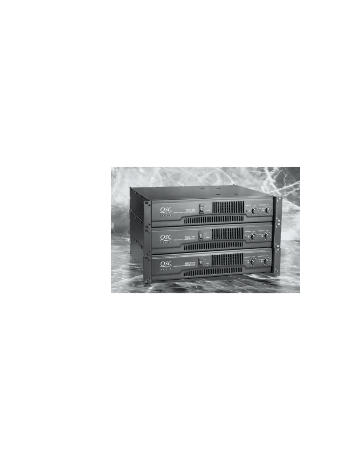
RMX™ Series
▲▲
▲ RMX 850
▲▲
▲▲
▲ RMX 1450
▲▲
▲▲
▲ RMX 2450
▲▲
Technical Service Manual
*TD-000098-00*
TD-000098-00
Rev. B

RMX Series
Technical Service Manual
RMX 850
RMX 1450
RMX 2450
QSC Audio Products, Inc.
Technical Services Group
Phone: 1-800 QSC AUDIO (1-800-772-2834) USA only
+1 (714) 957-7150
Fax: +1 (714) 754-6173
Postal: 1665 MacArthur Blvd.
Costa Mesa, California 92626 USA
E-mail: tech_support@qscaudio.com
Web: http://www.qscaudio.com (product information and support)
http://www.qscstore.com (parts and accessory sales)
Copyright 2001, 2002 QSC Audio Products, Inc. All rights reserved.
Document # TD-000098-00, Rev. B. Released February 2002.
RMX Series Technical Service Manual 1
RMX Series Performance Specifications
RMX 850 RMX 1450 RMX 2450
OUTPUT POWER
in watts
FTC: 20 Hz–20 kHz @ 0.1% THD, both channels driven
8Ω per channel 185 260 450
4Ω per channel 280 400 650
EIA: 1 kHz @ 0.1% THD, both channels driven
8Ω per channel 200 280 500
4Ω per channel 300 450 750
1 kHz @ 1% THD, typical, both channels driven
2Ω per channel 430 700 1200
Bridge Mono:
8Ω, 20 Hz–20 kHz, 0.1% THD 530 800 1300
8Ω, 1 kHz, 0.1% THD 600 900 1500
4Ω, 1 kHz, 1% THD, typical 830 1400 2400
DYNAMIC HEADROOM 2 dB @ 4Ω
DISTORTION
SMPTE-IM < 0.01% < 0.01% < 0.02%
FREQUENCY RESPONSE 20 Hz–20 kHz, +0/-1 dB
(at 10 dB below rated output power) -3 dB points: 5 Hz and 50 kHz
DAMPING FACTOR > 300 @ 8Ω
NOISE (unweighted 20 Hz to 20 kHz, below rated output) 100 dB 100 dB 100 dB
VOLTAGE GAIN 31.6× (30 dB) 40× (32 dB) 50× (34 dB)
INPUT SENSITIVITY, V RMS
full rated power @ 8Ω 1.15v (+3.4 dBu) 1.15v (+3.4 dBu) 1.23v (+4.0 dBu)
INPUT IMPEDANCE 10 KΩ unbalanced
20 KΩ balanced
CONTROLS Front: AC switch, Ch. 1 and Ch. 2 gain
Rear: 10-position DIP switch
INDICATORS POWER: Green LED CLIP: Red LED, 1 per channel
SIGNAL: Yellow LED, 1 per channel
CONNECTORS Input: Active balanced; XLR and ¼" (6.3 mm) TRS, tip and pin 2 positive, and barrier strip
Output: “Touch-Proof” binding posts and Neutrik Speakon™
COOLING Continuously variable speed fan, back-to-front air flow
AMPLIFIER PROTECTION Full short circuit, open circuit, thermal, ultrasonic, and RF protection
Stable into reactive or mismatched loads
LOAD PROTECTION Turn-on/turn-off muting, AC coupling, triac crowbar (on each channel)
OUTPUT CIRCUIT TYPE AB AB H
AB: Class AB complementary linear output
H: Class AB complementary linear output with Class H 2-step high efficiency circuit
DIMENSIONS 19.0" (48.3 cm) wide, 3.5" (8.9 cm) tall (2 rack spaces)
15.9" (40 cm) deep (rack mounting to rear support ears)
WEIGHT Shipping: 41 lb. (18.6 kg) 46 lb. (20.9 kg) 50.5 lb. (23 kg)
Net: 35 lb. (15.9 kg) 40 lb. (18.2 kg) 44.5 lb. (20.2 kg)
POWER REQUIREMENTS Available for 120 or 220–240 VAC, 50/60 Hz
POWER CONSUMPTION
(both channels driven)
Multiply currents by 0.5 for 230V units
@ 120 VAC
eldI
8
ΩΩΩΩΩ
4
ΩΩΩΩΩ
2
ΩΩΩΩΩ
1
2
lacipyT
lluF
A5.0
A3A1.4A4.7
A5.4A6.6A5.11
A5.6*A5.9*A71
3
xaM
8
ΩΩΩΩΩ
4
ΩΩΩΩΩ
2
ΩΩΩΩΩ
eldI
1
2
lacipyT
lluF
A5.0
A7.3A4.5A01
A6A6.9A61
A3.9*A7.41*A52
3
xaM
8
ΩΩΩΩΩ
4
ΩΩΩΩΩ
2
ΩΩΩΩΩ
eldI
1
lacipyT
A6.0
A4A7.9A4.61
A3.6A6.51A72
A2.9*A32*A14
2
3
lluF
xaM
US patents pending
SPECIFICATIONS SUBJECT TO CHANGE WITHOUT NOTICE
2 QSC Audio Products, Inc.

Table of Contents
RMX Series Performance Specifications ........................................................................................................................................ 4
1. Introduction ........................................................................................................................................................................................ 6
1.1 Service bulletins ................................................................................................................................................................................ 6
1.2 The well-equipped service bench ..................................................................................................................................................... 6
1.3 Working with surface-mount components ....................................................................................................................................... 6
1.4 Series description ............................................................................................................................................................................. 8
1.5 Technical descriptions and theory of operation ................................................................................................................................ 8
2. Component identification and pinout ........................................................................................................................................... 10
3. Troubleshooting: Symptoms, causes, & remedies ..................................................................................................................... 12
3.1 Excessive current draw ..................................................................................................................................................................... 12
3.2 Protection, muting, and turn-on/turn-off delay problems ................................................................................................................ 12
3.3 Faults with signal present ................................................................................................................................................................. 13
3.4 Instability ........................................................................................................................................................................................... 13
3.5 Power supply & rail balancing problems .......................................................................................................................................... 14
4. RMX calibration procedures .......................................................................................................................................................... 14
4.1 Setting bias ....................................................................................................................................................................................... 14
4.2 Setting positive and negative current limits ..................................................................................................................................... 15
5. Servicing RMX amplifiers ............................................................................................................................................................... 16
5.1 Mechanical disassembly and re-assembly ....................................................................................................................................... 16
6. Replacement parts ............................................................................................................................................................................ 17
6.1 RMX 850 Replacement Parts ............................................................................................................................................................ 17
6.2 RMX 1450 Replacement Parts .......................................................................................................................................................... 20
6.3 RMX 2450 Replacement Parts .......................................................................................................................................................... 23
7. Schematics and diagrams ............................................................................................................................................................... 27
7.1 RMX Assembly/Disassembly Diagram 1 of 2
7.2 RMX Assembly/Disassembly Diagram 2 of 2
7.3 RMX 850 Schematic Diagram 1 of 3
7.4 RMX 850 Schematic Diagram 2 of 3
7.5 RMX 850 Schematic Diagram 3 of 3
7.6 RMX 1450 Schematic Diagram 1 of 3
7.7 RMX 1450 Schematic Diagram 2 of 3
7.8 RMX 1450 Schematic Diagram 3 of 3
7.9 RMX 2450 Schematic Diagram 1 of 3
7.10 RMX 2450 Schematic Diagram 2 of 3
7.11 RMX 2450 Schematic Diagram 3 of 3
7.12 RMX 850 Chassis Wiring Diagram ................................................................................................................................................. 38
7.13 RMX 1450 Chassis Wiring Diagram ............................................................................................................................................... 39
7.14 RMX 2450 Chassis Wiring Diagram ............................................................................................................................................... 40
(All models) ...............................................................................................................
(All models) ...............................................................................................................
Channel 1 ...............................................................................................................................
Channel 2 ...............................................................................................................................
Power Supply .........................................................................................................................
Channel 1 .............................................................................................................................
Channel 2 .............................................................................................................................
Power Supply .......................................................................................................................
Channel 1 .............................................................................................................................
Channel 2 ...........................................................................................................................
Power Supply .....................................................................................................................
27
28
29
30
31
32
33
34
35
36
37
RMX Series Technical Service Manual 3

1. Introduction
1.1 Service bulletins
Contact QSC Technical Services to make sure you have the most up-to-date service bulletins for RMX Series amplifiers. Service bulletins
may be distributed in hard copy, via fax, and electronically (Adobe Acrobat PDF) via CD-ROMs, FTP from the QSC web site
(www.qscaudio.com), and e-mail.
These service bulletins had been issued at the time this manual was printed: RMX0001, “Q205 Lead Stress” (RMX 2450 only); RMX0002,
“RMX Turn-on Delay” (all RMX models); RMX0003, “RMX 2450 Turn-off Mute” (RMX 2450); RMX0004, “RMX 2450 AC Wire Routing”
(RMX 2450); RMX0005, “RMX 2450 AC Wire Replacement” (RMX 2450); and RMX0006, “RMX 2450 IRFZ44N Field Effect Transistors (RMX 2450).
1.2 The well-equipped service bench
To properly service RMX amplifiers, a technician needs the right tools. The technician’s service bench should have the following equipment:
• Digital multimeter with RMS AC voltage and current
• Digital clamp-on ammeter
• Dual-trace oscilloscope
• Audio distortion analyzer
• Non-inductive load resistors, configurable as 8 ohms (min. 500 watts capacity), as 4 ohms (min. 750 watts capacity), and 2 ohms (min.
1200 watts capacity)
• Variable AC voltage source, such as a Variac or Powerstat variable transformer, with a rated current capacity of up to 25A (for 120V
models) or 12A (for 230V models)
• Low-distortion audio sine wave generator
• Philips and flat screwdrivers
• Soldering iron with a fine tip (25–60W recommended)
• Rosin-core solder (60/40 or 63/37)
• Long-nose pliers
• Diagonal cutters
• Wire strippers
Automated test equipment, such as an Audio Precision workstation, is very useful for servicing RMX amplifiers. Contact QSC Technical
Services to obtain applicable AP test files.
1.3 Working with surface-mount components
RMX amplifiers, like many modern electronic products, use surface-mount technology (SMT) components where appropriate in order to
make high-density circuitry that is reliable and economical to manufacture.
SMT components in the RMX amps are used in the small-signal and control circuits, so they do not handle significant amounts of power;
therefore, they are subject to very little stress and should seldom fail. Sometimes they do fail, or they require replacement for a performance
upgrade or modification. Thus, it is important to know how to work with SMT components.
Specialized tools and equipment exist for soldering, unsoldering, and removing SMT components quickly and
efficiently, but they are often expensive. Most SMT repairs, though, can be handled reasonably well with common
tools and equipment, such as tweezers, solder braid, and fine-tip soldering irons. The original factory components
are tacked to the board with a spot of glue, so you might have to apply some force to break the adhesive.
Two-terminal components (resistors, capacitors, diodes, etc.)
Removal
1 Use two soldering irons, preferably about 25 to 40 watts, with fine tips.
2 With a soldering iron in each hand, hold one tip on the solder at one end of the component and the other
tip on the other end (Figure 1.1).
3 Once the solder melts on both ends, grip the component between the two tips and lift it from the circuit
board.
4 Use solder braid and a soldering iron to remove the solder from the two pads (Figure 1.2).
4 QSC Audio Products, Inc.
Figure 1.1.
Solder braid
Figure 1.2.
Solder
Figure 1.3.
Tweezers
Figure 1.4.
Figure 1.5.
Solder
Figure 1.6.
Solder
Insertion
1 With a soldering iron and 60/40 or 63/37 eutectic-type solder, melt just enough solder onto one pad to
create a small mound (Figure 1.3).
2 Grasp the component in the middle with tweezers. Melt the small mound of solder with the iron and
place the component across the two pads (in the correct orientation, if the component is sensitive to
direction) and press it flat against the circuit board, with one end of the component immersed in the
melted solder (Figure 1.4).
3 Hold the component in place and take the soldering iron away. Let the solder harden to tack the
component in place.
4 Fully solder the other end of the component to its pad. Let the solder harden (Figure 1.5).
5 Fully solder the tacked end of the component to its pad (Figure 1.6).
Three-terminal components (transistors, etc.)
Removal
1 With a soldering iron and solder braid, remove as much solder as possible from the middle terminal of
the component.
2 With a soldering iron in each hand, hold one tip on the solder at the terminal at one end of the compo-
nent and the other tip on the terminal at the other end.
3 When the solder on both ends melts, grip the component between the two tips and lift it from the circuit
board. You might need to quickly touch the pad on the middle terminal with a soldering iron to melt any
remaining solder that might be holding the component down.
4 Use solder braid and a soldering iron to remove the solder from the three pads.
Insertion
1 With a soldering iron and 60/40 or 63/37 eutectic-type solder, melt just enough solder onto one pad to create a small mound of solder.
2 Grasp the component with tweezers. Melt the small mound of solder with the iron and place the component in the correct orientation
across the three pads and press it flat against the circuit board, with one terminal of the component pressed into the melted solder.
3 Hold the component in place and take the soldering iron away. Let the solder harden to tack the component in place.
4 Fully solder the other terminals of the component to their pads. Let the solder harden.
5 Fully solder the tacked terminal of the component to its pad.
Multi-pin components (ICs, etc.)
Removal
Removing a multi-pin SMT component is a delicate procedure. Ideally, you should use a soldering iron with an attachment that allows you to
heat all the pins simultaneously.
If such a soldering device is not available, use this procedure:
1 Use a soldering iron and solder braid to remove as much solder as possible from the pins of the component.
2 With fine tweezers, carefully try to lift each pin to see if it’s free. If it’s not, touch it with the tip of the soldering iron and if necessary, use
the solder braid to remove the remaining solder.
3 Repeat the process until all the pins are free and you can remove the component.
Insertion
1 With a soldering iron and 60/40 or 63/37 eutectic-type solder, melt just enough solder onto one pad to create a small mound of solder. It
is usually easiest to use a pad that corresponds to one of the end or corner pins of the component.
2 Grasp the component with tweezers. Melt the small mound of solder with the iron and place the component in the correct orientation
upon its pads and gently press it flat against the circuit board, with the appropriate terminal of the component pressed into the melted
solder.
3 Hold the component in place and take the soldering iron away. Let the solder harden to tack the component in place.
4 Fully solder the other terminals of the component to their pads. Let the solder harden.
5 Fully solder the tacked terminal of the component to its pad.
RMX Series Technical Service Manual 5
1.4 Series description
QSC’s RMX Series amplifiers are entry-level professional audio
products, designed for good, basic performance and reliability at
low price. The series comprises three models: the RMX 850, RMX
1450, and RMX 2450. Each one has two audio channels and is two
rack spaces tall. See page 2 for complete specifications.
The RMX 850 and RMX 1450 have single-sided printed circuit
boards. The RMX 2450 uses double-sided boards.
1.5 Technical descriptions and
theory of operation
Note: Some of these descriptions concern circuitry that is duplicated
in the amplifier’s two channels. For the sake of simplicity, the
descriptions are of Channel 1 only. Components in Channel 1 have a
3-digit designation with “1” as
the first digit; their equivalents in
Channel 2 have a “2” as the first
digit, followed by the same two
numerals. For example, R122 and
R222 have identical functions in
their respective channels.
Power supplies
Figure 1.7
Unlike other recent QSC amplifiers,
the RMX line uses strictly conventional power supplies, with large
transformers that operate at the 50 or 60 Hz frequency of the AC
line. The electrical current in the secondary circuitry is converted to
DC through a full-wave bridge rectifier. The resulting 100 or 120 Hz
ripple is filtered out by large capacitors that also serve as current
reservoirs for short-term, transient demands.
The supply provides a bipolar set of supply rails for each channel, with
equal quiescent positive and negative voltages, as shown in Figure 1.7.
Note that unlike many bipolar supplies for complementary transistor
arrangements, the secondary windings are not connected to ground at
the center. This is because the output transistors are directly mounted
to the heat sink, metal-to-metal, to maximize heat transfer; this grounds
the collectors, requiring somewhat different output and power supply
arrangements. The grounded-collector concept is described later in
this chapter.
In the RMX 2450, the
secondaries are tapped to
provide an intermediate set
of bipolar rails for the Class H
output circuitry. Figure 1.8
shows one channel. Class H
operation is described later
in this chapter.
The 24-volt cooling fan is
driven by a separate DC
supply that is powered by a
Figure 1.8
To Channel 2 Center Tap
+Vcc
-Vcc
+Vcc
-Vcc
+110V
-110V
+55V
-55V
Ch. 1 Center Tap
0.047 µF
12 5W×2Ω
Channel 1
Channel 2
Channel 1
20-volt tap on the transformer primary. To minimize fan noise, the
fan speed is controlled by varying its actual DC voltage in response
to the amplifier’s heat sink temperatures. An optocoupler isolates
the fan control circuitry from the thermal sensors.
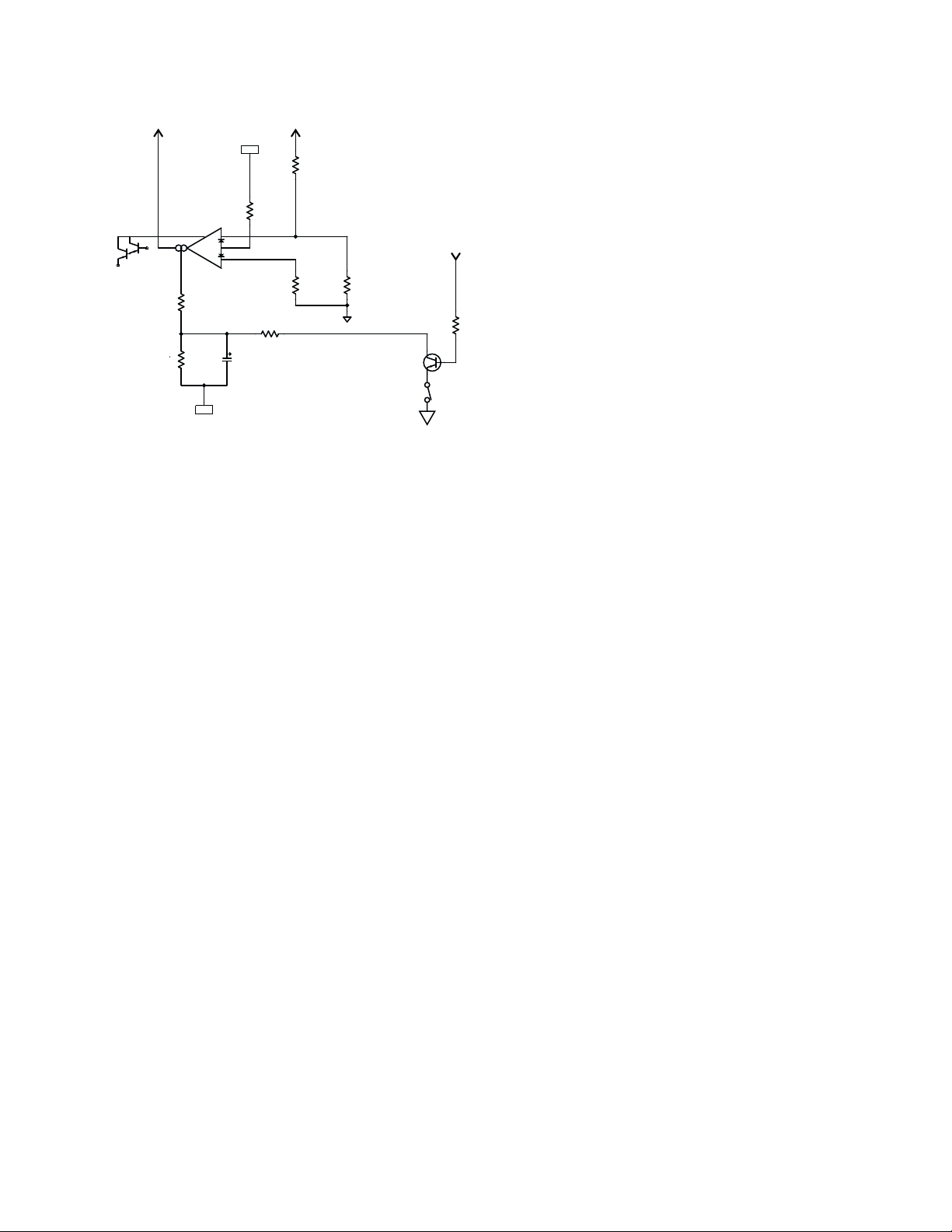
Audio circuitry
The audio inputs are balanced to offer a reasonably high amount of
common-mode noise rejection. The input balancing is done using a
single op amp (one half of an NE5532 dual op amp) arranged as a
differential amplifier. The degree of common-mode rejection is
dependent on a close match between the input resistors (R100 and
R101 in Figure 1.9) and between the feedback resistor and the shunt
resistor (R105 and R106). The circuitry uses 1% precision resistors
to ensure at least 40 dB of common-mode rejection.
C101
180p-5%
^C_0805
+IN_A
-IN_A
R100
10.0K
^R_0805
R101
10.0K
^R_0805
R102
1K
^R_0805
To LM13600 operational
transconductance amp
Figure 1.9
The feedback and shunt capacitors, C101 and C103, add a first-order
high-frequency roll-off, down 3 dB at 88.4 kHz (over two octaves
above the high end of the audio spectrum). This makes the amplifier
less susceptible to RF interference, high-frequency oscillations, etc.
Also in this stage, the feedback loop contains one half of a 13600 dual
operational transconductance amplifier (Figure 1.10). The OTA is part
of the clip limiter circuitry; when the clip limiter is activated, a control
voltage increases the transconductance of the OTA, which essentially decreases the impedance of the feedback loop and reduces
the gain of the stage in order to reduce the amount of clipping.
The gain control uses a linear potentiometer, but the impedances
loading the wiper to ground make the pot approximate an audio
taper over most of its rotation. After the wiper, RC networks roll off
the low end, if the LF filter is set for that channel, at either 30 or
50 Hz, depending on the DIP switch setting on the rear panel.
The next active device is another 5532 op amp, U101:2. Its output
drives the driver transistors, which in turn drive the output transistors.
The output section has a Class AB+B configuration; the drivers (a
complementary pair, Q105 and Q106, comprising an NPN MJE15032
and a PNP MJE 15033) are class AB. A series network of two diodes
and a 100-ohm trimpot provide the small amount of forward bias on
R105
10.0K
^R_0805
NE5532
U101:1
+
3
-
2
R106
10.0K
^R_0805
C103
180p-5%
A1
C106
1
10-50NP
R112
10K
10K LINEAR 3B
RIGHT ANGLE POT
CW
R113
W
270
^R_0805
CCW
A1
6 QSC Audio Products, Inc.
To input op amp U101:1
+14V
R108
7.50K
^R_0805
R107
U10:1
LM13600M
11
5
7
R103
R104
1
10.0K
^R_0805
150K
^R_1206
-14V
8
+
-
C105
39K
^R_0805
3
2
4
^R_0805
100
R111
^R_0805
A1
100-25V
R110
270
^R_0805
R109
100
3906
Q100
From clip
detection
820
R115
CLIP LIMIT
SWITCH
(Open to defeat
clip limiter)
^R_1206
Figure 1.10
the transistor pair to keep crossover distortion minimal. In parallel
with the trimpot is a 50-ohm thermistor with a negative temperature
coefficient; as the circuitry warms, its resistance decreases. This
reduces VBE on both Q105 and Q106, decreasing the bias current to
reduce the threat of thermal runaway. The base of each driver transistor
is tied to ground through a diode and a 2.2K trimpot in series; these set
the current limiting threshold for their respective signal polarities.
The collector of each driver transistor directly drives the bases of its
output transistors, which are the main power-handling signal
devices. If you’re not familiar with the grounded-collector scheme,
the arrangement of the output transistors might look somewhat
strange: the positive voltage swings are handled by PNP transistors,
while the negative swings are handled by NPN devices. The
collectors all connect to ground, which allows them to be mounted
directly to the heat sink—metal-to-metal, without insulators in
between—for the best possible transfer of heat away from the
transistors. The emitters of the PNP and NPN transistors are
coupled through resistors to the positive and negative supply rails,
respectively, forming banks of common-emitter circuits driving the
supply rails. Consequently, the devices drive the rails with the audio
signal, which rides atop the DC. The output to the speaker load is
taken from the point between the positive and negative reservoir
capacitors; this is also where the negative feedback is taken from.
The nature of this arrangement, with audio signal riding on the
supply rails, is why the power supply has no ground reference.
Another unusual characteristic of the grounded-collector output
section is that the signal at the output to the speaker is actually
opposite in polarity to the signal at the op amp output. This is why
the negative feedback resistor, R122, connects to the op amp’s non-
inverting input instead of the inverting input.
The output point of the circuit couples to the output connector
through an RLC network (R160, R161, R162, L100, and C124) that
serves as a high-frequency snubber and also helps keep the amp
circuitry stable when driving capacitive loads.
Clip detection
The output of the op amp also drives a group of four diodes (D102,
D103, D105, and D106) arranged as a full-wave rectifier. Normally,
the op amp’s output signal level is about 1 volt or less, which is all it
takes to drive the driver transistors.
But because this point is within the overall feedback loop, when
clipping occurs, the op amp approcahes full open-loop gain and puts
out a much higher signal voltage to try to make the output signal
track the input. The four diodes rectify the voltage to drive the clip
indicator LED, LD100. The current exiting the full-wave rectifier
passes to ground through R127 and also drives the base of
transistor Q100 through R115. If the clip limiter is switched on,
Q100’s emitter is grounded, and when the voltage across R127 goes
sufficiently negative to forward-bias Q100, which sends current
through R111 and R103 into the amplifier bias input of the operational transconductance amplifier (OTA), U10:1. The OTA is in the
negative feedback loop of U101:1, and increasing its
transconductance essentially reduces the impedance of the
feedback loop, which reduces the gain of the op amp stage. This
reduces the signal level until the amount of clipping is minimal.
When the clipping stops, Q100 is no longer forward-biased, and the
gain returns to normal.
DC protection
The RMX 2450 has a crowbar circuit, based on a triac and two
silicon controlled rectifiers, on the output to protect against DC
faults. If an amp channel puts out a DC voltage, which could be the
result of a component or circuit failure, it will first trigger either
D119 or D120, depending on the polarity of the voltage. The
triggered SCR will in turn trigger triac Q113, shorting the output to
ground through fuse F100. The fuse will blow, safeguarding the
speaker load from the DC fault.
The output sections of the RMX 850 and RMX 1450 are AC coupled.
Class H
The RMX 2450 utilizes a two-step Class H output section. It is
essentially a Class AB+B circuit but with two sets of bipolar supply
rails. On both the positive and the negative sets of rails, a comparator circuit, called a “step driver,” compares the audio signal to the
lower rail voltage. When necessary to fully reproduce the signal’s
voltage swing—just before the signal voltage reaches the lower rail
voltage—the step driver turns on a TMOS power FET to pull the
output transistors’ supply rail up from the lower voltage to the
higher one, and then back down again when the signal allows. By
keeping the transistors’ supply rails low whenever possible, the
devices dissipate less unused power and generate less waste heat,
making the amplifier more efficient than a straight class AB
amplifier with the same power points.
The comparators are 311-type ICs: U170 on the positive step and
U171 on the negative. Each one drives a high-gain complementary
transistor pair (2N3904 + 2N3906), which drive the gate of their
respective MOSFET.
RMX Series Technical Service Manual 7
Bridged mono operation and protection
When the amplifier is operated in bridged mono, its two channels
work in tandem to produce up to twice the voltage swing that a
single channel is capable of. To do this, Channel 2 produces a signal
identical to Channel 1’s, but opposite in polarity—in other words, a
mirror image.
Channel 2’s signal feed (bus BR_MONO_FEED) is an attenuated
version of the signal on Channel 1’s speaker bus. Closing DIP switch
#6 (set to “BRIDGE MONO ON”), connects the BR_MONO_FEED bus
on Channel 1 to the BR_RET bus on Channel 2. The BR_RET bus
drives the non-inverting input of op amp U201:2 directly.
With two channels operating as one, but each having its own
feedback and protection circuitry, it is vital to keep both running as
mirror images. A protection circuit monitors the balance between
Channel 1’s and Channel 2’s signals. Resistors R22 and R23 (R22A,
R22B, R23A, and R23B on the RMX 2450) are equal in value and
form a voltage divider between the two channel outputs. If the
output signals are mirror images, the voltage at the junction of the
resistors (bus BR_BAL) will be zero. If the signals are not mirror
images—for example, one channel is defunct, distorting, or reduced
in gain—a voltage will appear on BR_BAL. Through DIP switch 7,
the BR_BAL bus becomes bus BR_CUT and feeds the bases of
transistors Q8 and Q6, which are part of a 4-transistor circuit across
the +15V and -15V rails that supply the op amps and the input
circuitry. If the voltage on BR_CUT goes positive enough to forwardbias Q8, the transistor’s collector will collapse the +15V rail. At the
same time, the emitter current from Q8 will flow through R25 and
into the emitter of Q7, forward-biasing it, too. The collector of Q7
will then collapse the -15V rail.
Similarly, if BR_BAL goes sufficiently negative, it will forward-bias
Q6, in turn forward-biasing Q9, and these will collapse the ±15V rails.
With the rails collapsed, the op amp and the input circuitry will not
function, which will mute the audio.
2. Component identification and pinout
NE5532AN Dual operational amplifier
OUTPUT A
INVERTING
INPUT A
NON-INVERTING
INPUT A
V-
1
2
3
4
AB
V+
8
OUTPUT B
7
INVERTING
6
INPUT B
NON-INVERTING
5
INPUT B
LM311 Voltage comparator
GROUND 1
NON-INVERTING
INPUT
INVERTING
INPUT
1
2
3
V-
4
V+
8
OUTPUT
7
BALANCE/
6
STROBE
BALANCE
5
4N29 Opto-isolator
1
2
3
6
5
4
LM13600 Dual operational transconductance
amplifier
AMP BIAS INPUT A
DIODE BIAS A
NON-INVERTING
INPUT A
INVERTING INPUT A
OUTPUT A
BUFFER INPUT A
BUFFER OUTPUT A
1
2
3
4
5
V-
6
7
8
AB
AMP BIAS INPUT B
16
DIODE BIAS B
15
NON-INVERTING
14
INPUT B
INVERTING INPUT B
13
OUTPUT B
12
V+
11
BUFFER INPUT B
10
BUFFER OUTPUT B
9
2N5064 Sensitive gate thyristor
KAG
8 QSC Audio Products, Inc.
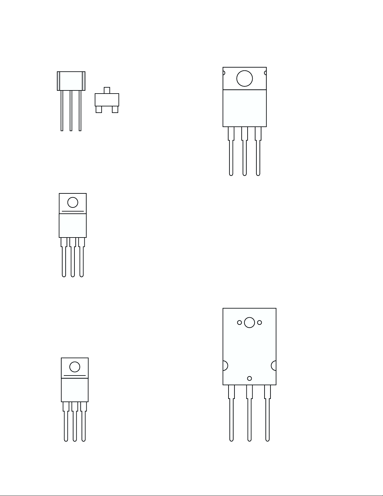
2N3904 (NPN) and 2N3906 (PNP) Small-signal
transistors
C
3
12
BE
BCE
IRFZ44 TMOS power field effect transistor
MAC224 Triac
G
MT1
MT2
MJE15032 (NPN) and MJE15033 (PNP) Driver
transistors
GDS
2SC5200 (PNP) and 2SA1943 (NPN) Power
transistors
TOSHIBA
BCE
RMX Series Technical Service Manual 9
B C E

3. Troubleshooting: Symptoms, causes, & remedies
When first checking the operation of an amplifier on the bench,
always turn your variable transformer down to zero before plugging
the amplifier in. After you turn the amplifier on, gradually turn up
the AC voltage as you observe the amplifier’s behavior and its
current draw; this will help you determine what, if anything, is
wrong with it. If you see or smell smoke, flames, or any other signs
of short circuits or excessive current draw, quickly turn the AC back
down to zero. If no such problems occur, it is usually safe to turn the
AC up to the amplifier’s full operating voltage for further testing.
3.1 Excessive current draw
The customer complains of blowing circuit breakers or fuses, or
burning smell or smoke.
Symptoms covered:
• Fuses blow immediately
• The amplifier quickly gets very hot
• Line circuit breakers trip at turn-on
• The amplifier hums loudly and the chassis vibrates
• The amplifier emits smoke
• The amplifier gives off a burning smell
If the symptoms indicate a possible problem in the channel circuits
or output sections, you can isolate either channel module from the
power supply by pulling its fuses from the AC board.
Possible situations:
Excessive current with no signal present
If the amplifier seems to run hot and draws higher-than-normal
current when idling at full AC voltage, the cause could be bias
misadjustments in the output circuitry of one or both channels. See
the calibration procedures in the next section. In the RMX 2450, the
cause might also be blown step FETs; see service bulletin RMX0006.
Fast increase in current draw (current increases rapidly at
only a few volts AC)
• The main bridge rectifiers BR100 and/or BR200 (all models) and
BR101 and/or BR201 (RMX 2450) is reversed or shorted.
• Supply clamp diode pairs D117 and D118 and/or D217 and D218
is reversed or shorted.
• The drivers and/or power transistors is shorted on both polarities
(NPN
and
PNP) on one or both channels.
Moderate increase in current draw (current increases
slowly, doesn’t become excessive until about ¼ of the
amplifier’s full AC operating voltage)
• One polarity’s drivers and/or power transistors (NPN or PNP) is
shorted, on one or both channels.
• Individual supply clamp diodes D117, D118, D217, or D218 is
reversed or shorted.
• Bias diodes D108, D109, D208, or D209 or bias trimpots R131 or
R231 is open.
Slow increase in current draw (current doesn’t become
excessive until about half of the amplifier’s full AC operating
voltage; amplifier may pass signal)
• The bias is severely misadjusted, or bias diodes D108, D109,
D208, or D209 is defective.
• An oscillation is causing excessive current demand.
Runaway current draw (current increases sharply at about
25 to 33% of the amplifier’s full AC operating voltage)
One or more reservoir capacitors is reversed. CAUTION: the gas
buildup in a reversed electrolytic capacitor can cause it to
vent explosively. Immediately turn off power and let the capacitor
cool down before replacing it.
3.2 Protection, muting, and turn-
on/turn-off delay problems
The customer complains of amplifier locking up, or not turning on
and off correctly.
Symptoms covered:
• Both channels do not come out of protect
• Amplifier will not thermally shut down when it should
• Power LED doesn’t light
• Too little or too much muting delay
• No clip limiting
• Fan doesn’t run, or runs always at high speed
Possible situations:
Both channels stay in protect after turn-on
• Q4 or Q5 is shorted base-to-emitter.
• Voltage across D8 should be 14 to 15 volts DC. If it is low, check
D8 and R10; also, C7 and C8 is leaky.
• D9, R4, and/or R7 is open.
The amplifier will not thermally shut down when it overheats
Check for shorted D9, R4, or R7; check also for open LD1 (“POWER”
LED), R2, or R5.
Too much or too little muting delay
• Excessive delay at turn-on: check for open LD1, R2, or R5; check
for incorrect R10 or R15; check for shorted D9; also see service
bulletin RMX0002.
• Too short at turn-on (amplifier unmutes before the circuits stabilize,
causing a thump): check for incorrect or bad C7, C8, or R10.
• Amplifier doesn’t stay muted at turn-off: see service bulletin RMX0003
Power LED doesn’t light
Check for open or shorted LD1; check R2.
No clip limiting
• U10 is defective.
• DIP switches SW1:1 or SW1:10 is defective.
10 QSC Audio Products, Inc.

Fan doesn’t run
• The fan is defective.
• Check the fan connection to the AC board.
• Check R1 and BR1 on the AC board.
Fan runs always on high speed
• Q3 and/or U2 are shorted.
• Check PTC thermistors R4 and R7.
• R130 or R132 (Channel 1) or R230 or R232 (Channel 2) is open.
Excessive hum in loudspeaker when no signal is present
(RMX 850 and RMX 1450)
Check R118, R119, R218, and R219.
Excessive current draw with signal present (RMX 2450)
• Check triacs Q113 and Q213.
• Check D119, D120, D219 and D220.
3.3 Faults with signal present
The customer compains that the amplifier passes a signal but
doesn’t run correctly.
Symptoms covered:
• The output signal breaks up or is distorted
•“Ringing” sound in loudspeaker when no audio signal is present
• The output signal collapses when driving a normal speaker load
• Supply rails OK with no signal, but collapse when a signal passes
• The amplifier gets too hot
• One channel clips prematurely
• Excessive hum in loudspeaker when no audio signal is present
Possible situations:
The output signal breaks up or is distorted
• (RMX 850 and RMX 1450) Check the hum-null resistors R118,
R119, R218, and R219.
• Check the ground traces for continuity among speaker ground,
input ground, and AC ground.
“Ringing” sound in loudspeaker when no audio signal is present
• Check C114, C124, C214 and C224.
• Check or replace dual op amp U101 or U201.
The output signal collapses when driving a normal speaker load
• R139, R140, R239, and/or R240 is misadjusted.
• Check R118, R119, R218, and R219.
The supply rails are OK with no signal but collapse with a signal
• C112, C113, C212, and/or C213 is leaky.
• Check C114, C124, C214, and C224.
The amplifier gets too hot with no load
• Bias trimpots R131 or R231 are misadjusted, burned, or open.
• Bias diodes D108, D109, D208 and/or D209 are incorrect (should
be 1N4934).
• If the amplifier is producing high-frequency oscillations, check
C114, C124, C214, and C224.
• Check resistors R136, R137, R236, and R237.
• Op amp U101 or U201 is unstable.
One channel clips prematurely
• R146 or R147 (Channel 1) or R246 or R247 (Channel 2) are open.
• R139 or R140 (Channel 1) or R239 or R240 (Channel 2) are misadjusted.
• Check R157, R158, R198 (RMX 2450 only), D115, and D116
(Channel 1) or R157, R258, R298 (RMX 2450 only), D215, and
D216 (Channel 2).
• (RMX 850 and RMX 1450) Check R118 and R119 (Channel 1) or
R218 and R219 (Channel 2).
3.4 Instability
The customer complains of gain problems, spurious noises, or oscillations.
Symptoms covered:
• General output distortion
•“Ringing” sound in loudspeaker trailing an audio signal
• Excessive crossover distortion
• The output waveform appears fuzzy on an oscilloscope
Distinguish among the different symptoms of fuzziness (instability),
ringing (momentary instability after a transition), crossover distortion (often causing ringing), or general distortion.
Possible situations:
General distortion in the output signal
• Severe distortion, at any load, often with abnormally high current
draw: check the slew rate capacitors C114, C115, and C116
(Channel 1) or C214, C215, and C216 (Channel 2).
• Moderate distortion, especially with light loading: stability
capacitors C124 and C126 (Channel 1) or C224 and C226 is too
high in capacitance; also check the slew rate capacitors C114,
C115, and C116 (Channel 1) or C214, C215, and C216 (Channel
2), and the output filter resistors R161, R162, R154, and R155
(Channel 1) or R261, R262, R254, or R255 (Channel 2).
• Distortion with low gain: check the feedback shunt components
R120, R138, and C125 (Channel 1) or R220, R238, or C225
(Channel 2); also check for broken circuit traces around the
components; U101 (Channel 1) or U201 (Channel 2) is defective
or its socket is contaminated.
Ringing sound trailing the audio signal
• This usually indicates marginal instability and is usually triggered
by the signal passing through zero volts (the crossover point).
Check the stability components and output filters.
• With a sine wave test signal, use an oscilloscope to check for
excessive crossover notch at the output signal’s zero crossings.
Excessive crossover distortion (unbalanced, asymmetrical,
or excessively large crossover notch)
• Severe crossover discontinuity: bias diodes D108 or D109
(Channel 1) or D208 or D209 (Channel 2) are shorted.
• Moderate discontinuity: bias diodes D108 or D109 (Channel 1) or
D208 or D209 (Channel 2) are out of spec.
• R131 (Channel 1) or R231 (Channel 2) is defective.
• Base resistors R136 or R137 (Channel 1) or R236 or R237
(Channel 2) are open. Also check the NTC thermistors R134
(Channel 1) or R234 (Channel 2).
RMX Series Technical Service Manual 11
 Loading...