

Page 1

MODEL
SERVICE MANUAL
DVD-400
CAUTION : Before servicing this chassis, read the "PRODUCT SAFETY SERVICE FOR VIDEO PRODUCTS" section
on page 2 of this manual.
CONTENTS
SERVICE PRECAUTIONS . . . . . . . . . . . . . . . . . . . . . . . 2,3
BLOCK DIAGRAMS . . . . . . . . . . . . . . . . . . . . . . . . . . . . . 4
IC INTRODUCTION . . . . . . . . . . . . . . . . . . . . . . . . . . . . . 5,18
PRINTED CIRCUIT . . . . . . . . . . . . . . . . . . . . . . . . . . . . . . 19,25
REPLACEMENT PARTS LIST . . . . . . . . . . . . . . . . . . . . . . 26,30
Page 2
PRODUCT SAFETY SERVICING GUIDELINES FOR VIDEO PRODUCTS
CAUTION: DO NOT ATTEMPT TO MODIFY THIS PRODUCT IN ANY WAY AND
NEVER PERFORM CUSTOMIZED INSTALLATIONS WITHOUT
MANUFACTURER'S APPROVAL. UNAUTHORIZED MODIFICATIONS WILL NOT
ONLY VOID THE WARRANTY, BUT MAY LEAD TO YOUR BEING LIABLE FOR
ANY RESULTING PROPERTY DAMAGE OR USER INJURY.
SERVICE WORK SHOULD BE PERFORMED ONLY AFTER YOU ARE
THOROUGHLY FAMILIAR WITH ALL OF THE FOLLOWING SAFETY CHECKS
AND SERVICING GUIDELINES. TO DO OTHERWISE, INCREASES THE RISK OF
POTENTIAL HAZARDS AND INJURY TO THE USER.
WHILE SERVICING, USE AN ISOLATION TRANSFORMER FOR PROTECTION
FROM A.C. LINE SHOCK.
SAFETY CHECKS
AFTER THE ORIGINAL SERVICE PROBLEM HAS BEEN CORRECTED, A CHECK
SHOULD BE MADE OF THE FOLLOWING.
SUBJECT: FIRE & SHOCK HAZARD
1. BE SURE THAT ALL COMPONENTS ARE POSITIONED IN SUCH A WAY AS
TO AVOID POSSIBILITY OF ADJACENT COMPONENT SHORTS. THIS IS
ESPECIALLY IMPORTANT ON THOSE MODULES WITCH ARE
TRANSPORTED TO AND FROM THE REPAIR SHOP.
2. NEVER RELEASE A REPAIR UNLESS ALL PROTECTIVE DEVICES SUCH AS
INSULATORS, BARRIERS, COVERS, SHIELDS, STRAIN RELIEFS, POWER
SUPPLY CORDS, AND OTHER HARDWARE HAVE BEEN REINSTALLED PER
ORIGINAL DESIGN. BE SURE THAT THE SAFETY PURPOSE OF THE
POLARIZED LINE PLUG HAS NOT BEEN DEFEATED.
3. SOLDERING MUST BE INSPECTED TO DISCOVER POSSIBLE COLD
SOLDER JOINTS, SOLDER SPLASHES OR SHARP SOLDER POINTS. BE
CERTAIN TO REMOVE ALL LOOSE FOREIGN PARTICLES.
4. CHECK FOR PHYSICAL EVIDENCE DF DAMAGE OR DETERIORATION TO
PARTS AND COMPONENTS, FOR FRAYED LEADS AND DAMAGED
INSULATION (INCLUDING A.C. CORD), AND REPLACE IF NECESSARY
FOLLOW ORIGINAL LAYOUT, LEAD LENGTH AND DRESS.
5. NO LEAD OR COMPONENT SHOULD TOUCH A RECEIVING TUBE OR A
RESISTOR RATED AT 1 WATT OR MORE. LEAD TENSION AROUND
PROTRUDING METAL SURFACES MUST BE AVOIDED.
6. ALL CRITICAL COMPONENTS SUCH AS FUSES. FLAMEPROOF RESISTORS,
CAPACITORS, ETC. MUST BE REPLACED WITH EXACT FACTORY TYPES,
DO NOT USE REPLACEMENT COMPONENTS OTHER THAN THOSE
SPECIFIED OR MAKE UNRECOMMENDED CIRCUIT MODIFICATIONS.
7. AFTER RE-ASSEMBLY OF THE SET, ALWAYS PERFORM AN A.C. LEAKAGE
TEST ON ALL EXPOSED METALLIC PARTS OF THE CABINET, (THE
CHANNEL SELECTOR KNOB, ANTENNA TERMINALS. HANDLE AND
SCREWS) TO BE SURE THE SET IS SAFE TO OPERATE WITHOUT DANGER
OF ELECTRICAL SHOCK. DO NOT USE A LINE ISOLATION TRANSFORMER
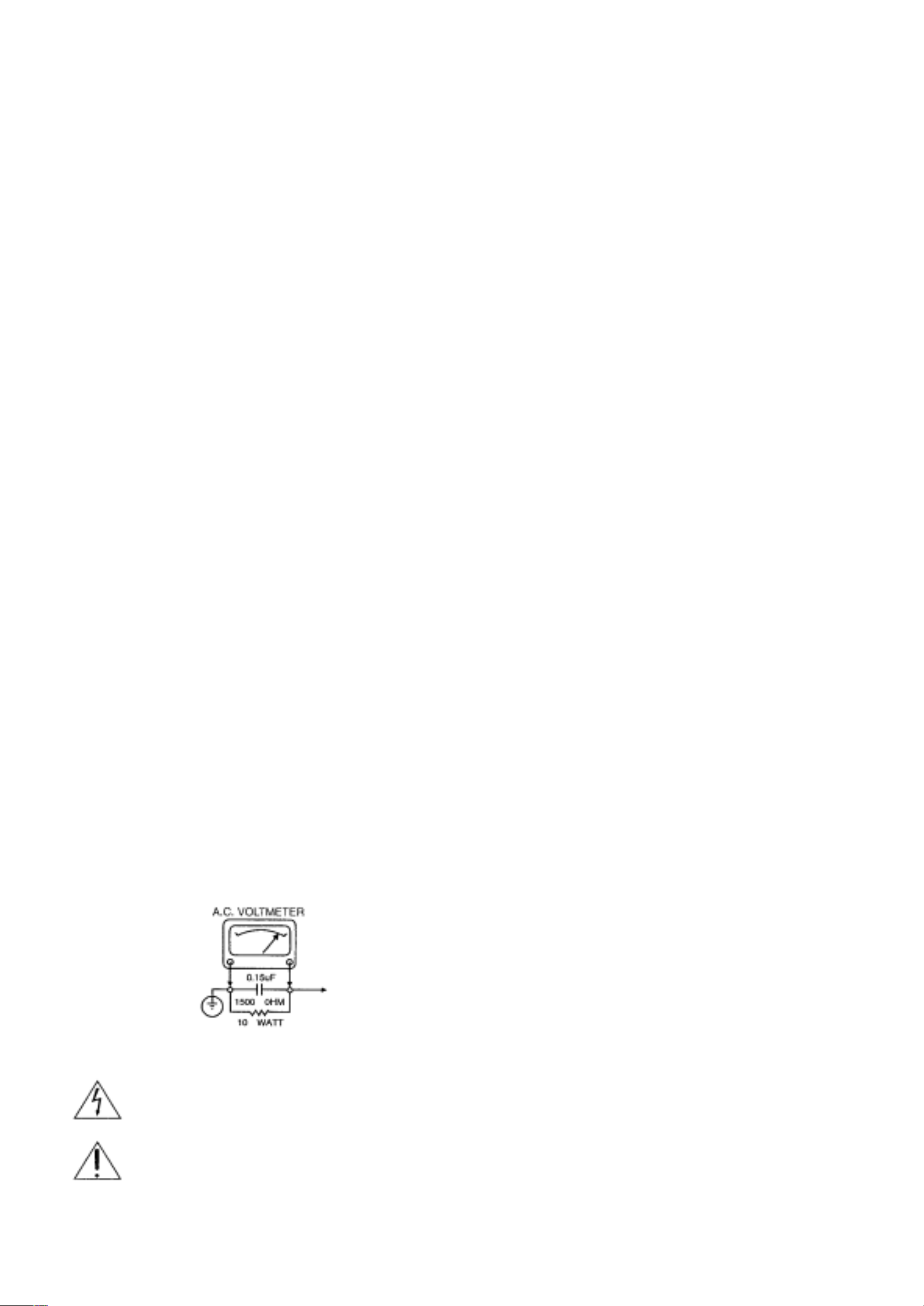
DURING THIS TEST, MAKE SURE TO USE AN A.C. VOLTMETER. HAVING
5000 OHMS PER VOLT OR MORE SENSITIVITY, IN THE FOLLOWING
MANNER; CONNECT A 1500 OHMS 10 WATT RESISTOR, PARALLELED BY
A.15 MFD. 150V A.C. TYPE CAPACITOR BETWEEN A KNOWN GOOD EARTH
GROUND (WATER PIPE, CONDUIT, ETC.) AND THE EXPOSED METALLIC
PARTS, ONE AT A TIME. MEASURE THE A.C. VOLTAGE ACROSS THE
COMBINATION OF 1500 OHM RESISTOR AND 15 MFD CAPACITOR.
REVERSE THE A.C. PLUG AND REPEAT A.C. ANY VOLTAGE
MEASUREMENTS FOR EACH EXPOSED METALLIC PART. VOLTAGE
MEASURED MUST NOT EXCEED 75 VOLTS R.M.S. THIS CORRESPONDS
TO 0.5 MILLIAMP A.C. ANY VALUE EXCEEDING THIS LIMIT CONSTITUTES A
POTENTIAL SHOCK HAZARD AND MUST BE CORRECTED IMMEDIATELY.
GOOD EARTH GROUND
SUCH AS THE WATER
PIPE, CONDUIT, ETC.
PLACE THIS PROBE
ON EACH EXPOSED
METAL PART
SUBJECT GRAPHIC SYMBOLS
THE LIGHTNING FLASH WITH APROWHEAD SYMBOL. WITHIN AN
EQUILATERAL TRIANGLE, IS INTENDED TO ALERT THE SERVICE
PERSONNEL TO THE PRESENCE OF UNINSULATED "DANGEROUS
VOLTAGE" THAT MAY BE OF SUFFICIENT MAGNITUDE TO
CONSTITUTE A RISK OF ELECTRIC SHOCK.
THE EXCLAMATION POINT WITHIN AN EQUILATERAL TRIANGLE IS
INTENDED TO ALERT THE SERVICE PERSONNEL TO THE
PRESENCE OF IMPORTANT SAFETY INFORMATION IN SERVICE
LITERATURE.
SUBJECT: X-RADIATION
1. BE SURE PROCEDURES AND INSTRUCTIONS TO ALL SERVICE PERSONNEL
COVER THE SUBJECT OF
X-RAYS IN CURRENT T.V. RECEIVERS IS THE PICTURE TUBE. HOWEVER,
THIS TUBE DOES NOT EMIT X-RYS WHEN THE HIGH VOLTAGE IS AT THE
FACTORY SPECIFIED LEVEL. THE PROPER VALUE IS GIVEN IN THE
APPLICABLE SCHEMATIC. OPERATION AT HIGHER VOLTAGES MAY CAUSE A
FAILURE OF THE PICTURE TUBE OR HIGH VOLTAGE SUPPLY AND, UNDER
CERTAIN CIRCUMSTANCES, MAY PRODUCE RADIATION IN EXCESS OF
DESIRABLE LEVELS.
2. ONLY FACTORY SPECIFIED C.R.T ANODE CONNECTORS MUST BE USED.
DEGAUSSING SHIELDS ALSO SERVE AS AN X-RAY SHIELD IN COLOR SETS,
ALWAYS RE-INSTALL THEM.
3. IT IS ESSENTIAL THAT SERVICE PERSONNEL HAVE AVAILABLE AN
ACCURATE AND RELIABLE HIGH VOLTAGE METER. THE CALIBRATION OF
THE METER SHOULD BE CHECKED PERIODICALLY AGAINST A
REFERENCE STANDARD, SUCH AS THE ONE AVAILABLE AT YOUR
DISTRIBUTOR.
4. WHEN THE HIGH VOLTAGE CIRCUITRY IS OPERATING PROPERLY, THERE IS
NO POSSIBILITY OF AN
CHASSIS IS SERVICED, THE BRIGHTNESS SHOULD BE RUN UP AND DOWN
WHILE MONITORING THE HIGH VOLTAGE WITH A METER TO BE CERTAIN
THAT THE HIGH VOLTAGE DOES NOT EXCEED THE SPECIFIED VALUE AND
THAT IT IS REGULATING CORRECTLY. WE SUGGEST THAT YOU AND YOUR
SERVICE ORGANIZATION REVIEW TEST PROCEDURES SO THAT VOLTAGE
REGULATION IS ALWAYS CHECKED AS A STANDARD SERVICING
PROCEDURE AND THAT THE HIGH VOLTAGE READING BE RECORDED ON
EACH CUSTOMER'S INVOICE.
5. WHEN TROUBLESHOOTING AND MAKING TEST MEASUREMENTS IN A
PRODUCT WITH A PROBLEM OF EXCESSIVE HIGH VOLTAGE AVOID BEING
UNNECESSARILY CLOSE TO THE PICTURE TUBE AND THE HIGH VOLTAGE
SUPPLY DO NOT OPERATE THE PRODUCT LONGER THAN IT IS NECESSARY
TO LOCATE THE CAUSE OF EXCESSIVE VOLTAGE.
6. REFER TO HV. B+ AND SHUTDOWN ADJUSTMENT PROCEDURES
DESCRIBED IN THE APPROPRIATE SCHEMATIC AND DIAGRAMS(WHERE
USED).
X-RADIATION. THE ONLY POTENTIAL SOURCE OF
X-RADIATION PROBLEM. EVERY TIME A COLOR
SUBJECT: IMPLOSION
1. ALL DIRECT VIEWED PICTURE TUBES ARE EQUIPPED WITH AN INTEGRAL
IMPLOSION PROTECTION SYSTEM, BUT CARE SHOULD BE TAKEN TO
AVOID DAMAGE DURING INSTALLATION, AVOID SCRATCHING THE TUBE. IF
SCRATCHED REPLACE IT.
2. USE ONLY RECOMMENDED FACTORY REPLACEMENT TUBES.
SUBJECT: TIPS ON PROPER INSTALLATION
1. NEVER INSTALL ANY PRODUCT IN A CLOSED-IN RECESS. CUBBYHOLE OR
CLOSELY FITTING SHELF SPACE, OVER OR CLOSE TO HEAT DUCT, OR IN
THE PATH OF HEATED AIR FLOW.
2. AVOID CONDITIONS OF HIGH HUMIDITY SUCH AS: OUTDOOR PATIO
INSTALLATIONS WHERE DEW IS A FACTOR, NEAR STEAM RADIATORS
WHERE STEAM LEAKAGE IS A FACTOR, ETC.
3. AVOID PLACEMENT WHERE DRAPERIES MAY OBSTRUCT REAR VENTING.
THE CUSTOMER SHOULD ALSO AVOID THE USE OF DECORATIVE
SCARVES OR OTHER COVERINGS WHICH MIGHT OBSTRUCT VENTILATION.
4. WALL AND SHELF MOUNTED INSTALLATIONS USING A COMMERCIAL
MOUNTING KIT, MUST FOLLOW THE FACTORY APPROVED MOUNTING
INSTRUCTIONS. A PRODUCT MOUNTED TO A SHELF OR PLATFORM MUST
RETAIN ITS ORIGINAL FEET (OR THE EQUIVALENT THICKNESS IN SPACERS)
TO PROVIDE ADEQUATE AIR FLOW ACROSS THE BOTTOM. BOLTS OR
SCREWS USED FOR FASTENERS MUST NOT TOUCH ANY PARTS OR
WIRING. PERFORM LEAKAGE TEST ON CUSTOMIZED INSTALLATIONS.
5. CAUTION CUSTOMERS AGAINST THE MOUNTING OF A PRODUCT ON
SLOPING SHELF OR A TILTED POSITION, UNLESS THE PRODUCT IS
PROPERLY SECURED.
6. A PRODUCT ON A ROLL-ABOUT CART SHOULD BE STABLE ON ITS
MOUNTING TO THE CART CAUTION THE CUSTOMER ON THE HAZARDS OF
TRYING TO ROLL A CART WITH SMALL CASTERS ACROSS THRESHOLDS
OR DEEP PILE CARPETS.
7. CAUTION CUSTOMERS AGAINST THE USE OF A CART OR STAND WHICH
HAS NOT BEEN LISTED BY UNDERWRITERS LABORATORIES, INC. FOR USE
WITH THEIR SPECIFIC MODEL OF TELEVISION RECEIVER OR
GENERICALLY APPROVED FOR USE WITH TV'S OF THE SAME OR LARGER
SCREEN SIZE.
8. CAUTION CUSTOMERS AGAINST THE USE OF EXTENSION CORDS. EXPLAIN
THAT A FOREST OF EXTENSIONS SPROUTING FROM A SINGLE OUTLET
CAN LEAD TO DISASTROUS CONSEQUENCES TO HOME AND FAMILY.
2
Page 3

SERVICING PRECAUTIONS
CAUTION : Before servicing the DVD covered by this
service data and its supplements and ADDENDUMS, read
and follow the SAFETY PRECAUTIONS NOTE : if
unforeseen circumstances create conflict between the
following servicing precautions and any of the safety
precautions in this publications, always follow the safety
precautions.
Remember Safety First:
General Servicing Precautions
1. Always unplug the DVD AC power cord from the AC
power source before:
(1) Removing or reinstalling any component, circuit board,
module, or any other assembly.
(2) Disconnection or reconnecting any internal electrical
plug or other electrical connection.
(3) Connecting a test substitute in parallel with an
electrolytic capacitor
Caution : A wrong part substitution or incorrect
polarity installation of electrolytic capacitors may
result in an explosion hazard.
Electrostatically Sensitive (ES) Devices
Some semiconductor (solid state) devices can be damaged
easily by static electricity. Such components commonly are
called Electrostatically Sensitive (ES) Devices. Examples of
typical ES devices are integrated circuits and some field
effect transistors and semiconductor chip components.
The following techniques should be used to help reduce the
incidence of component damage caused by static electricity.
1. Immediately before handling any semiconductor
component or semiconductor-equipped assembly, drain
off any electrostatic charge on your body by touching a
known earth ground. Alternatively, obtain and wear a
commercially available discharging wrist strap device,
which should be removed for potential shock reasons
prior to applying power to the unit under test.
2. After removing an electrical assembly equipped with ES
devices, place the assembly on a conductive surface
such as aluminum toil, to prevent electrostatic charge
buildup or exposure of the assembly.
2. Do not spray chemicals on or near this DVD or any of its
assemblies.
3. Unless specified otherwise in this service data, clean
electrical contacts by applying an appropriate contact
cleaning solution to the contacts with a pipe cleaner,
cotton-tipped swab, or comparable soft applicator.
Unless specified otherwise in this service data,
lubrication of contacts is not required.
4. Do not defeat any plug/socket B+ voltage interlocks with
witch instruments covered by this service manual might
be equipped.
5. Do not apply AC power to this DVD and/or any of its
electrical assemblies unless all solid-state device heat
sinks are correctly installed.
3. Use only a GROUNDED-tip soldering iron to solder or
unsolder ES devices.
4. Use only an anti-static solder removal device. Some
solder removal devices not classified a "anti-static" can
generate electrical charges sufficient to damage ES
devices.
5. Do not use freon-propelled chemicals. These can
generate electrical charge sufficient to damage ES
devices.
6. Do not remove a replacement ES device from its
protective package until immediately before you are
ready to install it. (Most replacement ES devices are
packaged with leads electrically shorted together by
conductive foam, aluminum foil, or comparable
conductive material.)
6. Always connect test instrument ground lead to the
appropriate ground before connection the test
instrument positive lead. Always remove the test
instrument ground lead last.
Insulation Checking Procedure
Disconnect the attachment plug trom the AC outlet and turn
the power on. Connect an insulation resistance meter(500V)
to the blades of the attachment plug. The insulation
resistance between each blade of the attachment plug and
accessible conductive parts (Note 1) should be more than
1M ohm.
Note 1 : Accessible Conductive Parts including Metal
panels, input terminals, Earphone jacks, etc.
3
7. Immediately before removing the protective material
from the leads of a replacement ES device, touch the
protective material to the chassis or circuit assembly
into which the device will be installed.
Caution : Be sure no power is applied to the chassis or
circuit, and observe all other safety precautions.
8. Minimize bodily motions when handling unpackaged
replacement ES devices. (Normally harmless motion
such as the brushing together of your clothes fabric or the
lifting of your foot from a carpeted floor can generate
static electricity sufficient to damage an ES device.)
Page 4
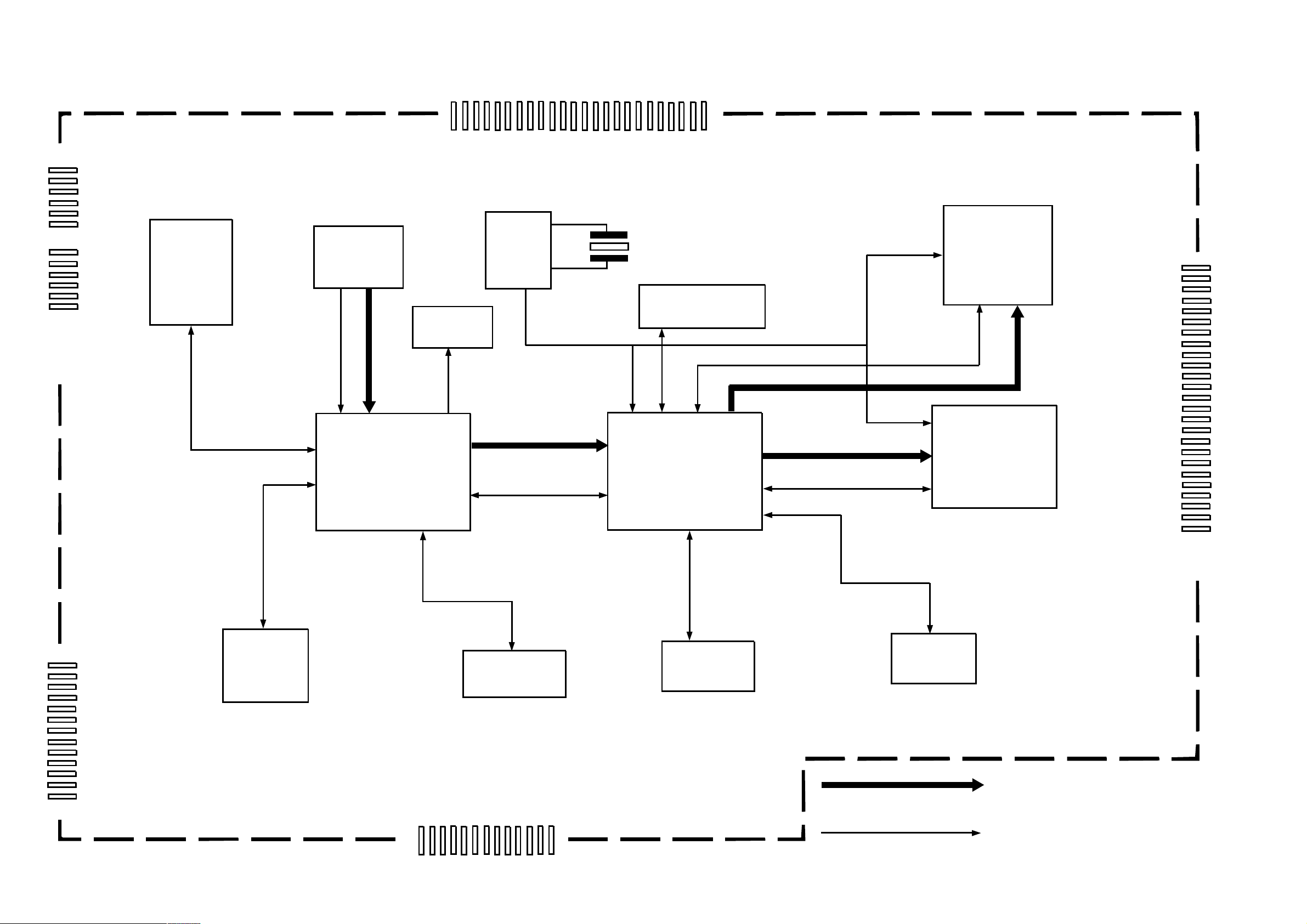
OVERALL BLACK DIAGRAM
XS100
XS103
SPSP+
LIM
GND
SLED+
SLED-
XS102
GND
CLOSE
GND
OPEN
UNLOD
LOAD
TO PICK UP
MECHANISM
CHASSIS
SERVO
& TRAY
DRIVER
BA5954
& BA6208
RF AMP
D1890
SERVO & DVD
PROCESSOR
D1870
TO PICK UP
MECHANISM
CHASSIS
F-F+T+T-NCBAEGNDVCVCCFDCCD/DVDNC(CD-LD)
TC4W53
HCUO4
27MHz
ATAPI
INTERFACE
VR-CD
VR-DVDMDLD-CD
AVCC
27MHz
16M SDRAM*2
MPEG-2
DECODER
VS2811
LD-DVD
GND
AUDIO DATA
VIDEO
ENCODER
CS4955
AUDIO DAC
PCM1723
&PCM1720
CHROMA
RED/AGND
LUMA
BLUE/AGND
CVBS2
VGND
GREEN/CVBS1
VGND
12V
GND
SPDIF
5V
ZERO
AGD
CEN
AGD
R-S
AGND
WOOF
AGD
L-S
AGD
L
AGD
R
XS107
RMC
FD ATA
FCS
FCLK
GND
3.5V
3.5V
24V
Vcc
12V
POWER
NC
NC
TO CONTROL ASSY
CONTROL
BUS
CPU
D1850
12V
POWER5V12V8VVcc
4M DRAM
3.3V
GND
GND
GND
24V
3.5V
3.5V
XS106
TO POWER
SUPPLY ASSY
EEPROM
24C01
XS109
TO OUTPUT ASSY
4M ROM
29F040
THE BUS OF THE DATA
CONTROL SIGNAL
Page 5
IC INTRODUCTION
D1890 PIN ASSIGNMENTS
Pin Numbers PIN NAME Type Description
QFP100 and LQFP100
RF Flag Interface
13 DEFECT Digital Output Flag of bad data output status
RF SIO interface
14 SLCK Digital Input RF serial clock input
15 SDEN Digital Input RF serial data enable
16 SDATA Digital IO RF serial data IO
11 RST Digital input Reset (active high)
12 XCK16M Digital input 16.9MHz for verification
RF
40 DVDA Analog input DVD RF signal input A
41 DVDB Analog Input DVD RF signal input B
42 DVDC Analog Input DVD RF signal input C
43 DVDD Analog Input DVD RF signal input D
38 DVDRFIN Analog Input DVD RF signal input RFIN
39 DVDRFIP Analog Input DVD RF signal input RFIP
53 CDA Analog Input CD RF signal input A
54 CDB Analog Input CD RF signal input B
55 CDC Analog Input CD RF signal input C
56 CDD Analog Input CD RF signal input D
61 OSP Analog Offset cancellation capacitor connecting
60 OSN Analog Offset cancellation capacitor connecting
86 RFOP Analog output RF positive output
85 RFON Analog output RF negative output
59 RFGC Analog RF VGA control
TRACKING ERROR
88 DPFN Analog DPD amplifier negative input
87 DPFO Analog DPD amplifier output
23 IR Analog DPD reference resister connecting
17 DPDMUTE Digital input DPD mute control input
83 TNI Analog Input 3 beam satellite PD signal input
82 TPI Analog Input 3 beam satellite PD signal input
97 TEO Analog Output Tracking error output
FOCUSING ERROR & RF LEVEL & CENTRAL SERVO SIGNAL
64 CDFNI Analog Input CD focusing error negative input
65 CDFPI Analog Input CD focusing error positive input
44 DVDFNI Analog input DVD focusing error negative input
45 DVDFPI Analog input DVD focusing error positive input
95 FEO Analog Output Focusing error output
96 FEONI Analog Input Focusing error amplifier negative input
93 FLVL Analog Output RF level output
5
Page 6

Pin Numbers PIN NAME Type Description
94 FLVLNI Analog input RF level amplifier negative input
69 CDCSNI Analog input CD central servo signal negative input
70 CDCSPI Analog input CD central servo signal positive input
46 DVDCSNI Analog input DVD central servo signal negative input
47 DVDCSPI Analog input DVD central servo signal positive input
2 CSO Analog output Central servo signal output
3 CSONI Analog input Central servo amplifier negative input
ALPC
80 MDI1 Analog Input Laser power monitor input
81 LDO1 Analog Output Laser driver output
51 MDI2 Analog Input Laser power monitor input
52 LDO2 Analog Output Laser driver output
RF RIPPLE
8 CRTP Analog RF top envelop filter capacitor connecting
9 CRTPLP Analog Defect level filter capacitor connecting
7 HRFRP Analog output High frequency RF ripple output
6 LRFRP Analog output Low frequency RF ripple output
POWER
24,25,30,34,62,63 AVDD Power RF power
21,22,28,37,57,58 AGND GND GND
89,90 SVDD Power Servo analog power
98,99 SGND GND GND
4,5 VDD Power Digital power
18,19 GND GND GND
REFERENCE VOLTAGE
92 VREFO Analog output Reference voltage 2.0V
91 V2REFO Analog output Reference voltage 4.0V
ALPC TRIMMING
32 TM1 Analog input Trimming pin for ALPC1
33 TM2 Analog input Trimming pin for ALPC1
35 TM3 Analog input Trimming pin for ALPC2
36 TM4 Analog input Trimming pin for ALPC2
HIGH SPEED TRACK COUNTING
1 TRLP Analog Low-pass filter capacitor connecting
100 TRLPA Analog Low-pass filter capacitor connecting
10 HTRC Digital output High speed track counting digital output
FOR MONITOR ONLY
26 MON Analog output
27 MOP Analog output
31 VCON Analog output
20 HTRCMPH Digital output
84 HTE Analog output
6
Page 7
D1890 BLOCK DIAGRAM
7
Page 8
D1870 PIN ASSIGNMENTS
Pin Numbers Pin NAME Type Description
RG data PLL interface
11 PLLVDD Power Power for data PLL and related analog circuitry.
10 JITFN Analog Input The negative input terminal of operation amplifier for RF jitter meter.
9 JITFO Analog Output The output terminal of RF jitter meter.
Phase comparator output. Output the phase difference of EFM and Pck4m.
8 PDO Analog Output
7 IREF Analog Input
6 LPFN Analog Input The negative input terminal of loop filter amplifier.
5 LPFO Analog Output The output of loop filter amplifier.
4 LPIN Analog Input The input of the low pass filter.
3 LPIO Analog Output The output of the low pass filter.
2 PLLVSS Ground Ground pin for data PLL and related analog circuitry.
1 VBDPLL Analog Output Reference voltage.
176 RFIN Analog Input The negative input terminal of RF differential signal.
175 RFIP Analog Input The positive input terminal of RF differential signal.
174 RFDSLV Analog Output RF data slicer level output.
173 SCO Analog Output Analog slicer current output.
Signal Amplifier Interface
172 ADCVDD Power Power pin for ADC circuitry.
171 HRFZC Analog Input High frequency RF ripple zero crossing input or photo interrupt pulse input.
170 RFRPSLV Analog Output RF ripple slice level output.
169 RFP Analog Input RF ripple detect input.
168 RFLEVEL Analog Input Sub beam add input or RF level input.
167 FEI Analog Input Focus error input.
166 TEI Analog Input Tracking error input.
165 TEZU Analog Input Tracking error zero crossing input.
164 TEZISLV Analog Input Tracking error zero crossing low pass input.
163 ADIN Analog Input General A/D input.
162 ADCVSS Ground Ground pin for ADC circuitry.
Motor and Actuator Drive Interface
161 PDMVSS Ground Ground for PDM Circuitry.
160 PWM2VREF Analog Input A reference voltage input for PWM circuitry. The typical value is 4.0V.
159 PWMVREF Analog Input A reference voltage input for PWM circuitry. The typical value is 2.0V.
158 PDMVDD Power Power for PDM circuitry.
12 FOO Analog Output Focus servo output. PDM output of focus servo compensator.
13 TRO Analog Output Tracking servo output. PDM output of tracking servo compensator.
14 PWMOUT1 Analog Output
15 PWMOUT2 Analog Output
17 DMO Analog Output Disk motor control output. PWM output.
18 FMO Analog Output
19
20 FG
22 TRCLOSE TTL Output
23 ENDM TTL Output Enable/disable disk motor. A logical high enables disk motor.
Panel Interface
FROPENPW
M
Analog Output
TTL Schmitt
Input 50K pull up
Sink or sour ce a constant c urrent to loop filt er over this pin w hen phase
difference occurs. Otherwise, this pin is high impedance.
Current reference input. It generates reference current for data PLL.
Connect an external 15K resistor to this pin and PLLVSS.
1
st General multi-level PW M output. Th e number of output lev els is set
with DSP command. It is used to control step motor.
2
nd Gener al multi-level PW M output. Th e number of ou tput level is
selected DSP command.
Disk motor control. 3-level PWM output. It is used only f or DC motor, but it
is corporate with the pin PWMOUT1 to control step motor. If the internal
DC_FMO is positive, the FMO output lags 90
the FMO output leads 90
Tray open control output.
It generates PWM output for TRWMEN
TRWMEN
Motor Hall sensor input.
Tray close output.
It provides a clock out to the micro controller.
27hRW2
=0.
than PWMOUT1.
than PWMOUT1, otherwise
=0 or digital out put for
27hRW2
8
Page 9
Pin Numbers Pin NAME Type Description
24 LED TTL Output LED control output.
25 PLY#/PAU#
26 EJ/STOP#
27 LIMIT#
28 TRAYOUT#
29 TRAYIN#
Micro controller Interface
30 URST TTL Output
31 UWR#
32 URD#
33 UCS1
34 UCS2
36 UALE
37-43,46 UAD
47 UINT#
Crystal Interface & DRAM clock Interface
44 DMVSS Ground Ground pin for DRAM clock circuitry.
45 DMVDD Power Power pin for DRAM clock circuitry.
48 XTALI Input Crystal input. The working frequency in 33.8688MHz.
49 XTALO Output Crystal output.
Memory Interface
50 DQM TTL Output
51 BA1 TTL Output
52 BA0 TTL Output
53 CKE TTL Output
54 CLK TTL Output SDRAM clock
55-56 RA[11:10] TTL Output
58-64,66-6
7,69
70 RAS# TTL Output RAM row address strobe, low active
71 ROE# TTL Output
RA[9:0] TTL Output RAM address bus
TTL Input
50K pull up
TTL Input
50K pull up
TTL Input
50K pull up
TTL Input
50K pull up
TTL Input
50K pull up
TTL Schmitt
Input 50K pull up
TTL Schmitt
Input 50K pull up
TTL I/O
50K pull up
TTL I/O
50K pull up
TTL I/O
with Schmitt
Input
50K pull up
TTL I/O
50K pull up
TTL Output
Open drain
Play/pause key input, active low.
Eject, stop key input, active low.
Sledge inner limit input, active low.
Tray_is_out input. A logical low indicates the tray is out. Feedback flag
from tray connector.
Tray_is_in input. A logical low indicates the tray is in. Feedback flag from
tray connector.
Power-on reset output for external devices, active high.
If the flash mode is used, the micro controller must be the kind of
multiplexed address/data mode and its output pins must be at tri-state.
Otherwise, the flash mode cannot be used.
Micro controller write strobe, active low.
Micro controller read strobe, active low.
For non flash mode cycle: register bank select control 1, input from micro
controller.
For flash mode cycle: flash ROM address FLASH_ADR14.
For non flash mode cycle: register bank select control 2, input from micro
controller.
For flash mode cycle: flash ROM address FLASH_ADR15.
For non fl ash mode c ycle: address latch en able, high active in put from
micro controller.
For flash mode cycle: address latch enable, high active output to control
external 373.
For non flash mode cycle: micro control address/data Bus.
For flash mode cycle: flash ROM address/data bus.
FLASH_ADR[7:0]/FLASH_D[7:0]. The FLASH_ADR[7:0] is latched in the
external 373.
Micro controller Interrupt, low active.
For non flash mode: SDRAM output Mask.
For flash mode: flash ROM address FLASH_ADR13.
For non flash mode: SDRAM bank address 1
For flash mode: flash ROM address FLASH_ADR12.
For non flash mode: SDRAM bank address 0
For flash mode: flash ROM address FLASH_ADR11.
For non flash mode: SDRAM clock enable.
For flash mode: flash ROM address FLASH_ADR10.
For non flash mode: DRAM address bus RA[11:10]
For flash mode: flash ROM address FLASH_ADR[9:8]
RAM output enable, low active.
It must be pulled with 20K resister if flash mode is used.
9
Page 10

Pin Numbers Pin NAME Type Description
72 RWE# TTL Output
73
74 CAS# TTL Output
76-83,
85-87
90-94
System Clock Interface
88 IPLLVDD Power Power pin for system varipitch circuitry.
89 IPLLVSS Ground Ground pin for system varipitch circuitry.
Host Interface
101 DASP#
102 CS3FX#
103 CS1FX#
105,108,10
6
107 PDIAG#
110 IOCS16#
CASH#/RWE
H#
RD[15:0] TTL I/O RAM data bus
HA[2:0]
TTL Output
TTL I/O
50K pull up
TTL Input
50K pull up
TTL Input
50K pull up
TTL Input
50K pull up
TTL I/O
50K pull up
TTL Output
Open drain
RAM write enable, low active. When two write enable pins are used, it only
for low byte.
High column address strobe: Write enable High Byte
Multi-function pin: low active
RAM column address strobe for high byte, when two column address
strobe pins are used.
Write enable for high byte, when two write enable pins are used.
World RAM column address strobe: Low column address strobe
Multi-function pin: low active
RAM column address strobe for a word, when two column address strobe
pins are not used.
It is used only for low byte, when two column address strobe pins are used.
Drive active/Slave present
This is the time-multiplexed sig nal that indi cates tha t a device is active, or
that slave is present.
Host chip select 2(for 3FXH/37xh)
The CX3FX# and CS1FX# are chip select signals from the host used to
select the Command Block registers.
Host chip select 1 (for 1Fxh/17xh)
Host address bus
This is the 3-bit binary coded address asserted by the host to access a
register or data port in the device.
Passed diagnostics
I/O 16-bit chip select
111 INTRQ TTL Output
112 DMACK#
113 IORDY TTL Output
114 DIOR#
TTL Input
50K pull up
TTL Input
50K pull up
Host interrupt.
The MT1368 uses this signal to interrupt the host system.
DMA acknowledge.
This signal shall be used by the host in response to DMAREQ to initiate
DMA transfers.
I/O channel ready: Ultra DMA ready: Ultra DMA data strobe.
This is a multi-function pin.
For i/o channel Ready, this signal is negated to extend the host transfer
cycle of any register read or write when the device is not able t o compl ete
the transfer.
For Ultr a DMA Read y, this signal is asserted by the devi ce to indic ate to the
host that the device is r eady to recei ve Ultra D MA data out bu rsts from the
host.
For Ultra DMA data strobe, this is the data in strobe signal from dev ice for
Ultra DMA data in burst to host.
Device I/O read: Ultra DMA ready: Ultra DMA data strobe.
This is multi-function pin.
For Device I/O Read, this signal is the strobe signal asserted by the host to
read device registers or the data port.
For Ultra DMA read, this is asserted by the host to indicate to the device
that the host is ready to receive Ultra DMA data in burst to host
For Ultra DMA data strobe, this signal is the data out strobe signal from the
host for an Ultra DMA data out burst.
10
Page 11

Pin Numbers Pin NAME Type Description
Device I/O write: Stop Ultra DMA burst
This is multi-function pin.
For Device I/O Write, this signal is the strobe signal asserted by the host to
write device registers or the data port.
116 DIOW#
TTL Schmitt
Input 50K pull up
For Stop Ultra DMA, this signal shall be negated by host before data is
transferred in an Ultra DMA burst and is asserted by host during an Ultra
DMA burst to signal the termination of Ultra DMA burst.
DMA request.
117 DMARQ TTL Output
This signal is used f or DMA dat a transfer s between host an d device a nd it
shall be asserted by the MT1368 when it is ready to transfer data to or from
the host. The direction of data transfer is controlled by DIOR# and DIOW #.
118 -120,12
2-126,-128-
131,134-13
HD[15:0] TTL I/O
7
138 HRST#
TTL Schmitt
Input 50K pull up
Host data bus.
This is an 8- or 16- bit bi-directional data interface between the host and
device; the lower 8 bits are used for 8-bit register transfers. Data transfers
are 16-bit wide.
Host reset.
This signal is referred to as hardware reset and it is used by host to reset
the MT1368.
CLV/CAV Varipitch interface
140 VPVDD Power Power pin for varipitch VCO circuitry.
141 VCOCIN Analog Input Connect capacitor for compensator loop filter.
142 VPVSS Ground Ground pin for varipitch VCO circuitry.
Miscellaneous
139 PRST#
TTL Schmitt
Power-on reset, low active
Input 50K pull up
143 TEST
TTL Input
Test mode control pin, high active
50K Pull-Down
Lag and Programmable I/O Interface
145 FLAGD TTL I/O Servo DSP flag.
146 FLAGC TTL I/O Servo DSP flag.
147 FLAGB TTL I/O Servo DSP flag.
Servo DSP flag. The internal flags of servo DSP can be selected to output
148 FLAGA TTL I/O
through FLAGA, FLAGB, FLAGC, and FLAGD pins. To program the
selection the micro controller must write FLGMOD register.
150 IO3
151 IO2
TTL I/O
50K pull high
TTL I/O
50K pull high
152 IO1 TTL I/O
153 IO0
TTL I/O
50K pull high
At non-flash mode: programm able I/O or internal non-servo flags output.
At flas h mode c ycle: to m onitor DSVSEL t o devic e master or slav er. It is
recorded on DEVSEL
At non-flash mode cyc le: progr ammable I/ O or int ernal non -servo fl ags outp ut.
At flash mode cycle: flash ROM address FLASH_ADR16.
At non-flash mode cyc le: progr ammable I/ O or int ernal non -servo fl ags outp ut.
At flas h mode cycle: flash ROM output enable FLASH_OE#.
At non-flash mode cyc le: progr ammable I/ O or int ernal non -servo fl ags outp ut.
At flas h mode cyc le: flas h ROM write enab le FLAS H_W R#.
102hRW6
.
SIO interface & Defect
154 SDATA TTL I/O RF serial data input/output.
155 SDEN TTL output RF serial data latch enable
156 SLCK TTL output RF serial clock output
157 BDO
TTL Input
Flag of defect data input status
50K pull down
Digital Power & Ground
57,75,104,1
DVDD3 Power +3.3V use for Internal digital circuitry and digital output pad
44
16,65,109,
DVDD Power +5V use for Internal digital circuitry and digital output pad
133,100
21,35,68,8
4,115,121,1
27,133,149
DVSS Ground Internal digital circuitry and digital output pad.
96
11
Page 12

D1870 BLOCK DIAGRAM
BDO
RFDTSL
SCO
RFIN
RFIP
PLLVDD
IREF
LPFN
LPIN
PLLVSS
JITFN
PDO
LPFO
LPIP
VBDPLL
JITFO
XTALO
XTALI
IPLLVDD
IPLLVSS
DMVDD
DMVSS
URST#
RFRPSLV
TEZI
TEZISLV
HRFZC
ADCVDD
FEI
TEI
RFRP
RFLEVEL
ADIN
ADCVSS
SLCK
SDEN
SDATA
FDO
TRO
FMO
PWMOUT1
PWMOUT2
PDMVDD
PWM2VREF
PWMVREF
PDWVSS
FLAGA
FLAGB
FLAGC
FLAGD
IO[3:0]
RFZC/
TEZC
Circuit
Servo
ADC
Serial RF
Controller
PDM &
PWM
DAC
Flags &
Program-
mable
I/O
RF flag
Interface
Servo
DSP
Varipitch
CLV Clock
Generator
VPVDD
VCOCIN
VPVSS
Data
Slicer
Sync
Protection
EFM/EFM+
Demodulator
Subcode/ID
Demodulator
CLV/CAV
Controller
FG
ENDM
Data
PLL
PWM
DAC
DMO
CIRC/RSPC
Error Corrector
CDROM
Sync Detection
Descrambler
CSS
Host/MPEG Interface
HRST#
DASP#
PDIAG#
HD[15:0]
Host
Data
FIFO
DIOR#
DIOW#
Decoder
HA[2:0]
CS1FX#
DMACK#
C3
ATAPI
Packet
FIFO
CX3FX#
Varipitch System
INTRQ
IORDY
DMARQ
IOCS16#
Clock
Generator
System Clock
Micro-controller
Interface
UALE
UCS1
UCS2
URD#
UWR#
256
SRAM
UINT#
DRAM
Clock
Generator
UAD[7:0]
Reset
Logic
Buffer
Memory
Controller
Key/LED
Interface
Mega
Interface
TEST
PRST#
RD[15:0]
RA[11:0]
RAS#
CAS#
CASH#/RWEH#
RWE#
ROE#
CLK
CKE
DOM
BA(1:0)
EJ/STOP#
PLY#/PAU#
LED
TRAYIN#
TRAYOUT#
LIMIT#
TROPENPWM
TRCLOSE
12
Page 13

VS3811 PIN ASSIGNMENTS
Name Number I/O Definition
1,9,18,27,35,44,51,59,68,75,83,92,99
VCC
LA[21:0] 23:19,16:10,7:2,207:204 O Device address output.
VSS
RESET# 24 I Reset input, active low.
TDMDX
RSEL
TDMDR 28 I TDM receive data.
, 104, 111,121,130,139,148,157,164,
172, 183, 193,201
8,17,26,34,43,52,60,67,76,84,91,98,1
03,112,120,129,138,147,156163,171,
177,184,192,200,208
O TDM transmit data.
25
3.6 V power supply.
I
Ground.
I
ROM Select
RSEL Selection
I
0 16-bit ROM
1 8-bit ROM
TDMCLK 29 I TDM clock input.
TDMFS 30 I TDM frame synch.
DMTSC# 31 O TDM output enable, active low.
TWS 32 O Audio transmit frame sync.
Select P ll1.
SEL-PLL2 SEL-PLL0 Clock Output
0 0 2.5*DCLK
SEL_PLL[2:0] 33 I
0 1 3*DCLK
1 0 3.5*DCLK
1 1 4*DCLK
TSD[3:0] 38,37,36,33 O Audio transmit serial data port.
MCLK 39 I/O Audio master clock for audio DAC.
TBCK 40 I/O Audio transmit bit clock.
SPDIF_DOB
41 O
M
S/PDIF (IEC958) Format Output.
RSD 45 I Audio receive serial data.
RWS 46 I Audio receive frame synch.
RBCK 47 I Audio receive bit clock.
APLLCAP 48 I Analog PLL Capacitor.
XIN 49 I Crystal input.
XOUT 50 O Crystal output.
DMA[11:0] 66:61,58:53 O DRAM address bus.
DCAS# 69 O Column address strobe, active low.
O Output enable, active low. DOE#
70
DSCK_EN
DWE# 71 O DRAM write enable, active low.
DRAS[2:0]# 74:72 O Row address strobe, active low.
Clock Enable, active low.
I
13
Page 14

Name Number I/O Definition
DB[15:0] 96:93,90:85,82:77 I/O DRAM data bus.
DCS[1:0]# 97,100 O SDRAM chip select [1:0], active low
DQM 101 O Data input/output mask.
DSCK 102 O Clock to SDRAM.
DCLK 105 I Clock Input (27 MHz)
YUV[7:0] 115:113,110:106 O 8-bit YUV output.
PCLK2XSC
2X pixel clock.
116 I/O
N
PCLKQSCN 117 I/O Pixel clock.
Vertical synch for screen video
VSYNCH# 118 I/O
interface, programmable for rising or
falling edge, active low.
Horizontal sync for screen video
HSYNCH# 119 I/O
interface, programmable for rising or
falling edge, active low.
HD[15:0] 141:140,137:131,128:122 O Host data bus
HCS1FX# 152 O Host select 1.
HCS3FX# 153 O Host select 3.
HIOCS16# 151 I Device 16-bit data transfer.
HA[2:0] 158,155:154 I/O Host address bus.
Peripheral protection voltage. See
VPP 159 I
App Note 2.
Host write/DCI Interface Acknowledge
HWR#/DCI_A CK#
149 I,O
Signal, active low.
HRD#/DCI_CLK
O,
150
Host read/DCI Interface Clock.
O
HD[15:0] 141:140,137:131,128:122 I/O Host data bus.
HWRQ# 142 O Host write request.
HRDQ# 143 O Host read request.
HIRQ 144 I/O Host intrrupt.
HRST# 145 O Host reset.
HIORDY 146 I Host I/O ready
AUX[7:0] 169:165,162:160 I/O Auxiliary ports.
LOE# 170 O Device output enable, active low.
LCS[3:0]# 176:173 O Chip select [3:0], active low.
LD[15:0] 197:194,191:185,182:178 I/O Device data bus.
LWRLL# 198 O Device write enable, active low.
LWRHL# 199 O Device write enable, active low.
NC 37,38,42,203:202 No Connect pins. Leave open.
14
Page 15

VS3811 BLOCK DIAGRAM
15
Page 16

CS4955 PIN ASSIGNMENTS
PIN NAME NUMBER TYPE DEFINITION
V[7:0] 8,7,6,5,4,3,2,1 IN Digital video data inputs
CLK 29 IN 27MHz input clock
PADR 16 IN Address enable line
XTAL-IN 15 IN Sub-carrier crystal input
XTAL-OUT 14 OUT Sub-carrier crystal output
HSYNC/CB 10 I/O Active low horizontal sync, or composite blank signal
VSYNC 11 I/O Active low vertical sync
FIELD/CB 9 OUT Video field ID. Selectable polarity or composite blank
RD 27 IN Host parallel port read strobe, active low
WR 28 IN Host parallel port write strobe, active low
PDAT[7:0] 19,20,21,22,23,24,25,26 I/O Host parallel port/general purpose I/O
SDA 32 I/O I C data
SCL 33 IN I C clock input
CVBS 44 CURRENT Composite video output
Y 48 CURRENT Luminance analog output
C 47 CURRENT Chrominance analog output
R 39 CURRENT Red analog output
G 40 CURRENT Green analog output
B 43 CURRENT Blue analog output
VREF 38 I/O Internal voltage reference output external reference input
SET 37 CURRENT DAC current set
TTXDAT 30 IN Teletext data input
TTXRQ 31 OUT Teletext request output
INT 12 OUT Interrupt output, active high
RESET 34 IN Active low master RESET
TEST 13 IN Test pin. Ground for normal operation
VAA 36,41,46 PS +5V or +3.3Vsupply(must be same as VDD)
GNDD 18 PS Ground
VDD 17 PS +5V or +3.3Vsupply(must be same as VAA)
GNDA 35,42,45 PS Ground
CS4955 BLOCK DIAGRAM
16
Page 17

PCM1723 PIN ASSIGNMENTS
PIN NAME NUMBER TYPE DEFINITION
XTI 1 IN Master clock input
SCKO 2 OUT
VCP 3 PWR PLL Power Supply (+5v)
NC 4 N/A No connection
MCKO 5 OUT Buffered clock output of crystal oscillator
ML 6 IN Latch for serial control data
MC 7 IN Clock for serial control data
MD 8 IN Data for serial control
RSTB 9 IN
ZERO 10 OUT
VOUTR 11 OUT Right Channel Analog Output
AGND 12 GND Analog Ground
VCC 13 PWR Analog Power Supply(+5v)
VOUTL 14 OUT Left Channel Analog Output
CAP 15 Common pin for analog output amplifiers
BCKIN 16 IN Bit clock for clocking in the audio data
DIN 17 IN Serial audio data input
LRCIN 18 IN Left/Right Word Clock. Frequency is equal to fs
NC 19 N/A No connection
RES 20 N/A Reserved for factory use, do not connect
VDD 21 PWR Analog Power Supply(+5v)
DGND 22 GND Digital Ground
PGND 23 GND PLL Ground
XTO 24 OUT Crystal oscillator output
Note:(1)Schmitt triger input with int ernal pull-up resistors.
(2)Schmitt triger input.
System Clock Out. This output is 256fs or 384fs.System clock generated
by the internal PLL.
Reset input. When this pin is low, the digital filters and modulator are held
in reset
Zero Data Flag. This pin is low when the input data is continuously zero for
more than 65.535 cycles of BCKIN
PCM1723 BLOCK DIAGRAM
17
Page 18

BA6208 EQUIVALENT CIRCUIT DIAGRAM
VCC GND
6(1)
5(3,7)
R1
R32
Q1
Q3
Q2
R2
R30
D1
Q6
Q4
R3
R4
R5
R7
R11
R6
R13
Q5
R12
R28
Q7
R9
Q9
R8
Q8
7(2)
BOUT
AIN
3(8)
Q10
Q11
BIN
8(4)
AOUT
2(5)
Q12
R15
R16
Q14
Q13
Q15
R20
R29
R14
R18
R21
R19
R22
R23
Q16
Q19
R24
R25
Q17
R31
D2
Q18
R26
R27
Q20
R10
R17
NOTE : Figures in parentheses are for the BA6208F
BA6208 INPUT/OUTPUT TRUTH TABLE
AIN
H
L
L
H
AOUTBIN
H
L
BOUT
L
H
HH
LL
L
OPEN
BA6208 EXTERNAL DIMENSIONS
1
BA6208
9
L
OPEN
8
1
BA6208F
5
4
18
Page 19

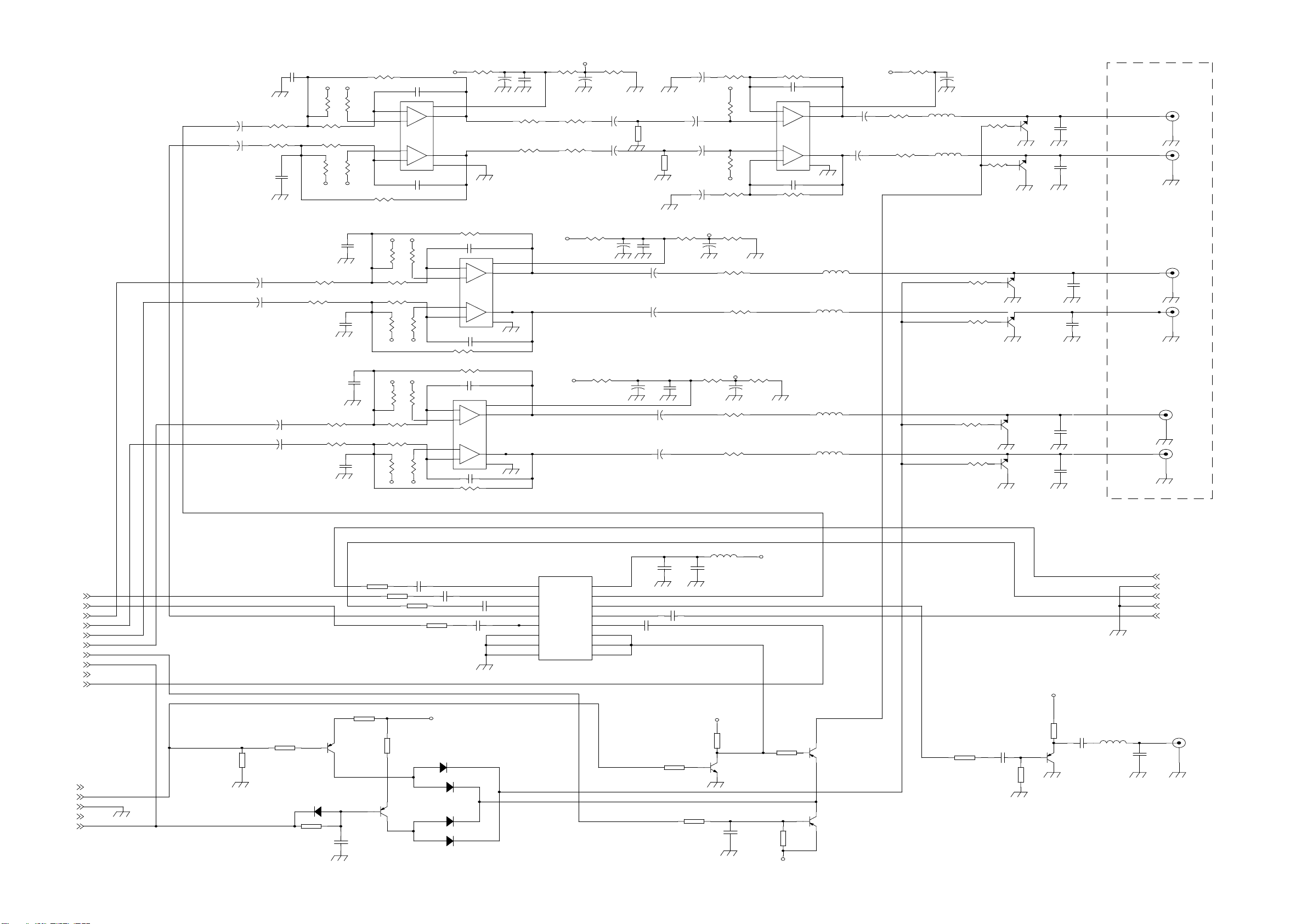
POWER
S505
VFD20-0501
F1
P1P2P3P4P5P7P8P9P10
F1
30
272625242321201918171615141312
29
P6
22
P11
P12
P13
P16
P17
P18
5G4G3G2G1GF2F2
87654
2
1
D168BK CONTROL CIRCUIT
XP501
RMC
DATA
STB
CLK
GND
F1
F2
-24V
CONTROL 5V
+5V
NG
POWER
B501
RMC
GND
VCC
1
2
3
C502
100U/6.3V
R514
100
R513
100
C504
100U/6.3V
C501
0.1U
R512
10
Q501
LED1
VD503
IN4148
C503
0.1U
R508
4.7K
R503
10K
R502
10K
R501
10K
R511
56K
1
2
3
4
5
6
7
8
9
10
11
12
13
SW1
SW2
SW3
SW4
DOUT
DIN
IC
CLK
STB
KEY1
KEY2
KEY3
KEY4
40
41
42
43
44
45
46
47
48
49
50
51
52
G4
G3
G2
VSS
OSD
LED2
LED1
LED3
LED5
LED4
G1
VDD
D501
UPD16311
VDDS1S2S3S4S5S6S7S8S9S10
14151617181920212223242526
S11
G5
S12
G6
G7
G8
S20
S19
VEE
VDD
S18
S17
S16
S15
S14
S13
39
38
37
36
35
34
33
32
31
30
29
28
27
S1
S2
VD503
IN4148
VD502
IN4148
S504
STOP
S501
OPEN/CLOSE
S502
PLAY
S503
PAUSE
R509 1K
R504 10K
R505 10K
R506 10K
R507
10K
Page 20

12V
GND
GND
xp303
L301
POWER-in(12V)
20U
VD301
4002
R303
R302
2K
1K
C301
100uf/25
C306
103
R301
24K
R303
560
C306
102
R302
0.15/1W
+
C307
471
x
104
N305
3843BN
1
2
3
45
R305
C308
222
10K
8
7
6
1
R308
100
N301
7809
OUT
IN
GND
2
x
2.2
x
1N4148
C310
104
R310
56K
R307
22
3
+
R309
1K/1W
VD308
21DQ10
N307
IRFZ44
x
22
C311
47UH/50
C302
100/16
C312
474
C313
331
VD307
FR102
N302 CW7805
1
IN
C303
OUT
GND
2
3
C034
100/16
104
VD311
3605
T1
w301
R300
10
R31810
XP302
5V(K)
5V
+
C305
R306
100k
104
v322
709
R317
1k
N302 CW7805
1
VD302
3605
C322
104
VD305
MA152
IN
R313
1K
C316
47U/50V
OUT
GND
2
C321
10K
3
100/16
C320
102
VD303
3401
C034
L302
20UH
C314
1000U/16V
C317
470V/16V
+
R312
1K
L303
20UH
R314
390
C318
470U/10V
C325
470u/10V
N304
1499
R316
22
VD306
5A1
C319
47U/16V
R315
390
GND
POWER ON\OFF
9V
XP301
5V
POWER ON\OFF
5V(K)
7V
NC
5V(K)
3.8V
GND
GND
GND
-24V
F2
F1
DC168A POWER CIRCUIT
C315
47U/16V
VD304
3401
Page 21
c213
10UF
c214
10UF
c215
2200p
c216 2200p
R222
0
R227
0
R228
3.9k
R221
100K
R218
100K
VccAVccA
R223
3.9k
VccAVccA
R220
10K
R219
10K
R224
10K
R230
10K
VccB
C225
R234
12V
100
C218
330PF
8
-
+
AN4558
N203
+
-
V+
V-
C217
330PF
7
1
4
6
5
3
2
100U
C219
104
R226
R231
12k
R232
4.7K
12k
R229
R225
15k
15k
C224
47U
R233
4.7K
C228
10UF
C226
10UF
R238
3k
R235
3k
C231
47UF
C229
10UF
C227
C230
47UF
10UF
VCCA
VccA
R236
3K
R240
R237
3K
100K
100K
R239
R243
33k
C223 56p
6
-
5
+
N202
AN4558
3
+
2
-
C222 56p
R242
33k
8
V+
7
1
4
V-
C232
10UF
C233
10UF
12V
R244
100
100
R245
100
R241
C234
100U
L202 600
L203 600
R246
1K
R247
1K
V208
MC9014
V207
MC9014
C220
330P
C221
330P
C240
0.22UF
C239
0.22UF
C248
0.22u
C247
10u
R263
6.2k
R264
6.2k
C237
2200p
C253
2200P
C238
2200p
R279
R278
6.2k
C254
2200P
6.2k
VccD VccD
R266
100K
R262
3.9K
R261
3.9K
R265
100K
VccD
VccE VccE
R281
100K
R277
3.9K
R276
3.9K
R280
100K
VccD
VccEVccE
R267
10K
R268
10K
R282
10K
R283
10K
R260
10K
C235
330PF
6
-
5
+
N204
AN4558
3
+
2
-
C236 330PF
R259 10K
R275
10K
6
-
5
+
N205
AN4558
3
+
2
-
C251
330PF
R274
10K
C252
330PF
V+
V-
R257
12V
R256
100
C241
8
V+
7
1
4
V-
8
7
1
4
100U
C243
10u
C244
10u
12V VccE
R271
100
C250
100U
C260
104
C261
104
C245
10U
C246
10UF
4.7K
C242
47U
VccD
R272
4.7K
C249
47U
100
R270
100
R269
100
R254
R258
4.7K
R255
100
R273
4.7K
R252 0
R253 0
L205 600
L206
V209
R248
1K
R249
1K
R250
600
1K
R251
1K
MC9014
V210
MC9014
V211
MC9014
V212
MC9014
C257
330p
C258
330p
330p
330p
C255
C256
X202
12v
power on
gnd
+5vc
5v
F-R
F-L
S-L
SUB
S-R
CENT
ZERO
5V
RMC
V
R201
470
R202
2k
R210
10k
VD201
iss355
12
2sb709
V203
+
R212
100
C204
470u
R205
12k
R217
7.5k
R206
12k
R213
100
2sb709
V206
C209 10u
+
R216
7.5k
+5vc
1 2
C212
10u
+
VD204
1ss355
1 2
VD202
Iss355
1 2
VD203
Iss355
1 2
C211
10u
VD205
Iss355
L204
600
+
R215
10k
C208
100u
12v
R204
1.5k
V201
mc9014
C206
100U
C202
0.1u
+
R203
10k
C207
+
100U
VCC
U1
16
15
Y
14
X
13
X1
12
X0
11
A
10
B
4053
1
Y1
2
C210
10u
+
+
Y0
3
Z1
4
Z
5
Z0
6
EN
7
VEE
8 9
GND C
C259
0.1u
12v
R
GND
L
GND
V
+5V
R211
10k
R214
10k
V204
2sb709
V205
2sb709
R207
100
+
R209
200
C205
100u
R208
10k
OUT168216 OUTPUT CIRCUIT
2sb709
V202
C203
470u
+
L201
600
C201
330p
+5vc
Page 22

168BK PCB DIAGRAM
Page 23

DC168A POWER PCB DIAGRAM
Page 24

OUT168216 OUTPUT DIAGRAM
Page 25

DSM5016CM DECODER PCB DIAGRAM
Page 26

ELECTRICAL PARTS LIST
PART No. PART NAME Q'TY
DVD400
1034 D168BK CONTROL ASS'Y 1
0865 OUT168216 OUTPUT ASS'Y 1
0854 DC168A POWER ASS'Y 1
0866 DSM5016CM DECODER ASS'Y 1
S2295 KHL231BM MECHANISM ASS'Y 1
S1642 OWNER MANUAL 1
S3230 D168 AUDIO CORD 1
S3231 D168 VIDEO CORD 1
S3118 OPEN W IRE 1
S3119 SERVO W IRE 1
S3214 CC-0.5×33×200 1
S3126 CC-1.0×12×150 1
S3216 CC-1.0×25×40 1
S3219b D168 POWER CORD ASS'Y 1
04003 REMOTE CONTROL ASS'Y 1
S0588 6.2mH INDUCTOR ASS'Y 1
S0676s RC-168 REMOTE 1
S2701a BATTERY 2
02006 DVD168B AV INPUT ASS'Y 1
Page 27

REF No. PART No. PART NAME REF No. PART No. PART NAME
D168BK CONTROL ASS'Y
R501 G0735 RT13-0.167W-10K±5% R211 P11013 RC-03K103JT
R502 G0735 RT13-0.167W-10K±5% R212 P11006 RC-03K101JT
R503 G0735 RT13-0.167W-10K±5% R213 P11006 RC-03K101JT
R504 G0735 RT13-0.167W-10K±5% R214 P11013 RC-03K103JT
R505 G0735 RT13-0.167W-10K±5% R215 P11013 RC-03K103JT
R506 G0735 RT13-0.167W-10K±5% R216 P11054 RC-03K752JT
R507 G0735 RT13-0.167W-10K±5% R217 P11054 RC-03K752JT
R508 G0728 RT13-0.167W-4.7K±5% R218 P11019 RC-03K104JT
R509 G0719 RT13-0.167W-1K±5% R219 P11013 RC-03K103JT
R511 G0784 RT13-0.167W-56K±5% R220 P11013 RC-03K103JT
R512 G0705 RT13-0.167W-10±5% R221 P11019 RC-03K104JT
R513 G0712 RT13-0.167W-100±5% R222 P11000 RC-03K000JT
R514 G0712 RT13-0.167W-100±5% R223 P11031 RC-03K392JT
CAPACITOR
R210 P11013 RC-03K103JT
R224 P11013 RC-03K103JT
C501 a3540 CD11CX-100uF-M-6.3V R225 P11015 RC-03K153JT
C502 a3304 CT4D-2F4-0.1uF-63V-S R226 P11014 RC-03K123JT
C503 a3540 CD11CX-100uF-M-6.3V R227 P11000 RC-03K000JT
C504 a3304 CT4D-2F4-0.1uF-63V-S R228 P11031 RC-03K392JT
TOUCH
S501 G6434 EVQ21504M(4.5mm) R230 P11013 RC-03K103JT
S502 G6434 EVQ21504M(4.5mm) R231 P11015 RC-03K153JT
S503 G6434 EVQ21504M(4.5mm) R232 P11012 RC-03K472JT
S504 G6434 EVQ21504M(4.5mm) R233 P11012 RC-03K472JT
S505 G6434 EVQ21504M(4.5mm) R234 P11006 RC-03K101JT
OTHER
B501 a6733 HS0038B RECEIVER R236 P11052 RC-03K302JT
VD501 a5004 IN4148 R237 P11052 RC-03K302JT
VD502 a5004 IN4148 R238 P11052 RC-03K302JT
VD503 a5004 IN4148 R239 P11019 RC-03K104JT
R229 P11014 RC-03K123JT
R235 P11052 RC-03K302JT
LED a1500
D501 P4399 PT6311 R241 P11006 RC-03K101JT
V501 a6871 VFD-20-0501 R242 P11017 RC-03K333JT
XP501 P6569 12FPZ-SM-TF R243 P11017 RC-03K333JT
OUT168216 OUTPUT ASS'Y
R201 P11008 RC-03K471JT R245 P11006 RC-03K101JT
R202 P11010 RC-03K202JT R246 P11009 RC-03K102JT
R203 P11013 RC-03K103JT R247 P11009 RC-03K102JT
R204 P11051 RC-03K152JT R248 P11009 RC-03K102JT
R205 P11014 RC-03K123JT R249 P11009 RC-03K102JT
R206 P11014 RC-03K123JT R250 P11009 RC-03K102JT
R207 P11006 RC-03K101JT R251 P11009 RC-03K102JT
R208 P11013 RC-03K103JT R252 P11205 0
R209 P110567 RC-03K201JT R253 P11205 0
ø3 RED LED
R240 P11019 RC-03K104JT
R244 P11006 RC-03K101JT
Page 28

REF No. PART No. PART NAME REF No. PART No. PART NAME
R254 P11006 RC-03K101JT C213 a3509 CD110-10uF-M-16V
R255 P11006 RC-03K101JT C214 a3509 CD110-10uF-M-16V
R256 P11006 RC-03K101JT C215 P20042 GRM39B222K50PT
R257 P11012 RC-03K472JT C216 P20042 GRM39B222K50PT
R258 P11012 RC-03K472JT C217 P20029 GRM39CH331J50PT
R259 P11013 RC-03K103JT C218 P20029 GRM39CH331J50PT
R260 P11013 RC-03K103JT C219 P20015 GRM39F104Z25PT
R261 P11031 RC-03K392JT C220 P20029 GRM39CH331J50PT
R262 P11031 RC-03K392JT C221 P20029 GRM39CH331J50PT
R263 P11142 6.2K C222 P20037 GRM39CH560J50PT
R264 P11142 6.2K C223 P20037 GRM39CH560J50PT
R265 P11019 RC-03K104JT C224 a3512 CD110-47uF-M-16V
R266 P11019 RC-03K104JT C225 a3513 CD110X-100uF-M-10V
R267 P11013 RC-03K103JT C226 a3509 CD110-10uF-M-16V
R268 P11013 RC-03K103JT C227 a3509 CD110-10uF-M-16V
R269 P11006 RC-03K101JT C228 a3509 CD110-10uF-M-16V
R270 P11006 RC-03K101JT C229 a3509 CD110-10uF-M-16V
R271 P11006 RC-03K101JT C230 a3512 CD110-47uF-M-16V
R272 P11012 RC-03K472JT C231 a3512 CD110-47uF-M-16V
R273 P11012 RC-03K472JT C232 a3509 CD110-10uF-M-16V
R274 P11013 RC-03K103JT C233 a3509 CD110-10uF-M-16V
R275 P11013 RC-03K103JT C234 a3513 CD110X-100uF-M-10V
R276 P11031 RC-03K392JT C235 P20029 GRM39CH331J50PT
R277 P11031 RC-03K392JT C236 P20029 GRM39CH331J50PT
R278 P11142 6.2K C237 P20042 GRM39B222K50PT
R279 P11142 6.2K C238 P20042 GRM39B222K50PT
R280 P11019 RC-03K104JT C239 a3502 CD110-0.22uF-M-16V
R281 P11019 RC-03K104JT C240 a3502 CD110-0.22uF-M-16V
R282 P11013 RC-03K103JT C241 a3513 CD110-100uF-M-16V
R283 P11013 RC-03K103JT C242 a3512 CD110-47uF-M-16V
R284 P11003 RC-03K100JT C243 a3509 CD110-10uF-M-16V
CAPACITOR
C244 a3509 CD110-10uF-M-16V
C201 P20029 GRM39CH331J50PT C245 a3509 CD110-10uF-M-16V
C202 P20015 GRM39F104Z25PT C246 a3509 CD110-10uF-M-16V
C203 a3516 CD110X-470uF-M-16V C247 a3509 CD110-10uF-M-16V
C204 a3516 CD110X-470uF-M-16V C248 a3502 CD110-0.22uF-M-16V
C205 a3513 CD110-100uF-M-16V C249 a3512 CD110-47uF-M-16V
C206 a3513 CD110-100uF-M-16V C250 a3513 CD110-100uF-M-16V
C207 a3513 CD110-100uF-M-16V C251 P20029 GRM39CH331J50PT
C208 a3513 CD110-100uF-M-16V C252 P20029 GRM39CH331J50PT
C209 a3509 CD110-10uF-M-16V C253 P20042 GRM39B222K50PT
C210 a3509 CD110-10uF-M-16V C254 P20042 GRM39B222K50PT
C211 a3509 CD110-10uF-M-16V C255 P20029 GRM39CH331J50PT
C212 a3509 CD110-10uF-M-16V C256 P20029 GRM39CH331J50PT
Page 29

REF No. PART No. PART NAME REF No. PART No. PART NAME
C257 P20029 GRM39CH331J50PT
DC168A POWER ASS'Y
C258 P20029 GRM39CH331J50PT R301 P11037 RC-03K273JT
C259 P20015 GRM39F104Z25PT R302 P11010 RC-03K202JT
C260 P20015 GRM39F104Z25PT R303 P11009 RC-03K102JT
C261 P20015 GRM39F104Z25PT R304 P11050 RC-03K561JT
INDUCTOR
R305 P11013 RC-03K103JT
L201 P6817 BSZ2012-600T3 R306 P11013 RC-03K103JT
L202 P6817 BSZ2012-600T3 R307 a0707 RT13-1/16W-22±5%
L203 P6817 BSZ2012-600T3 R308 a0712 RT13-1/16W-100±5%
L204 P6817 BSZ2012-600T3 R309 a0498 RY16-1W-1K±5%
L205 P6817 BSZ2012-600T3 R310 P11039 RC-03K563JT
L206 P6817 BSZ2012-600T3 R311 a0499 RY17-1W-0.1±10%
DIODE
R312 P11009 RC-03K102JT
VD201 P1200 ISS355TE17 R313 P11009 RC-03K102JT
VD202 P1200 ISS355TE17 R314 P11130 RC-03K391JT
VD203 P1200 ISS355TE17 R315 P11130 RC-03K391JT
VD204 P1200 ISS355TE17 R316 a0707 RT13-1/16W-22±5%
VD205 P1200 ISS355TE17 R317 P11009 RC-03K102JT
TRIODE
V201 P5073a 2SD601AR
R318 P11000 RC-03K000JT
CAPACITOR
V202 P5700 2SB709AR C301 a3520 CD110X-220uF-M-25V
V203 P5700 2SB709AR C302 a3609 CD110X-100uF-M-25V
V204 P5700 2SB709AR C303 P20015 GRM39F104Z25PT
V205 P5700 2SB709AR C304 a3609 CD110X-100uF-M-25V
V206 P5700 2SB709AR C305 P20015 GRM39F104Z25PT
V207 P5073a 2SD601AR C306 P20012 GRM39B103K50PT
V208 P5073a 2SD601AR C307 P20008 GRM39B471K50PT
V209 P5073a 2SD601AR C308 P20009 GRM39B102K50PT
V210 P5073a 2SD601AR C309 P20009 GRM39B102K50PT
V211 P5073a 2SD601AR C310 P20015 GRM39F104Z25PT
V212 P5073a 2SD601AR C311 a3210 CD110X-47uF-M-50V
IC
C312 a2078 CS09Y5V63V224S
D201 P4595 BU4053BCF-E2 C313 a2037 CC1-10B-471K-63V-SL
N201 P4503 NJM4558M C314 a3709 CD110X-1000uF-10V±20%
N202 P4503 NJM4558M C315 a3210 CD110X-47uF-M-50V
N203 P4503 NJM4558M C316 a3210 CD110X-47uF-M-50V
N204 P4503 NJM4558M C317 a3709 CD110X-1000uF-10V±20%
OTHER
C318 a3561 CD110X-470uF-M-10V
X201 a6982 AV-8.4-4A(YELLOW) C319 a3635 CD110X-47uF-M-16V
X202 a6999 AV6-8.4-1 C320 P20009 GRM39B102K50PT
X203 a6662 HSJ1715-01110 C321 P20015 GRM39F104Z25PT
XP201
XP202
a6521 S-5B-PH C322 P20015 GRM39F104Z25PT
a6521 S-5B-PH C323 a3609 CD110X-100uF-M-25V
XP203 a6613 FABSE2552 C324 a3609 CD110X-100uF-M-25V
Page 30

REF No. PART No. PART NAME
C325 a3561 CD110X-470uF-M-10V
TRANSISTOR
VD301
VD302
VD303
VD304
VD305
VD306
VD307
VD308
VD312 a1560 11EFS2
V322 P5700 2SB709AR
N301 a4714 CW7809
N302 a4571 CW7805
N304 a5063 3DD3852P
a5001 IN4002
P5722 RB060L-40
P5721 RB160L-40
P5721 RB160L-40
P1556 MA152
a1571 4C3
a1224 1U08
a1224 1U08
IC
N305 a4716 AP3843
N308 a5116 IRF244N
N309 a4571 CW7805
OTHER
XP301 a6874 B-13B-PH
XP302 a8834
XP303 a6975 WII-2AW
L302 a6272 20mH
L303 a6272 20mH
L304 a6994 200uH
W301 a6993 EPC25 TRANSFORMER
DC168A POWER CORD
 Loading...