

Philips NE83Q92A20, NE83Q92N, NE83Q92A, NE83Q92D Datasheet
INTEGRATED CIRCUITS
NE83Q92
Low-power coaxial Ethernet transceiver
Product specification
IC19 Data Handbook
1995 May 01
Philips Semiconductors Product specification
NE83Q92Low-power coaxial Ethernet transceiver
DESCRIPTION
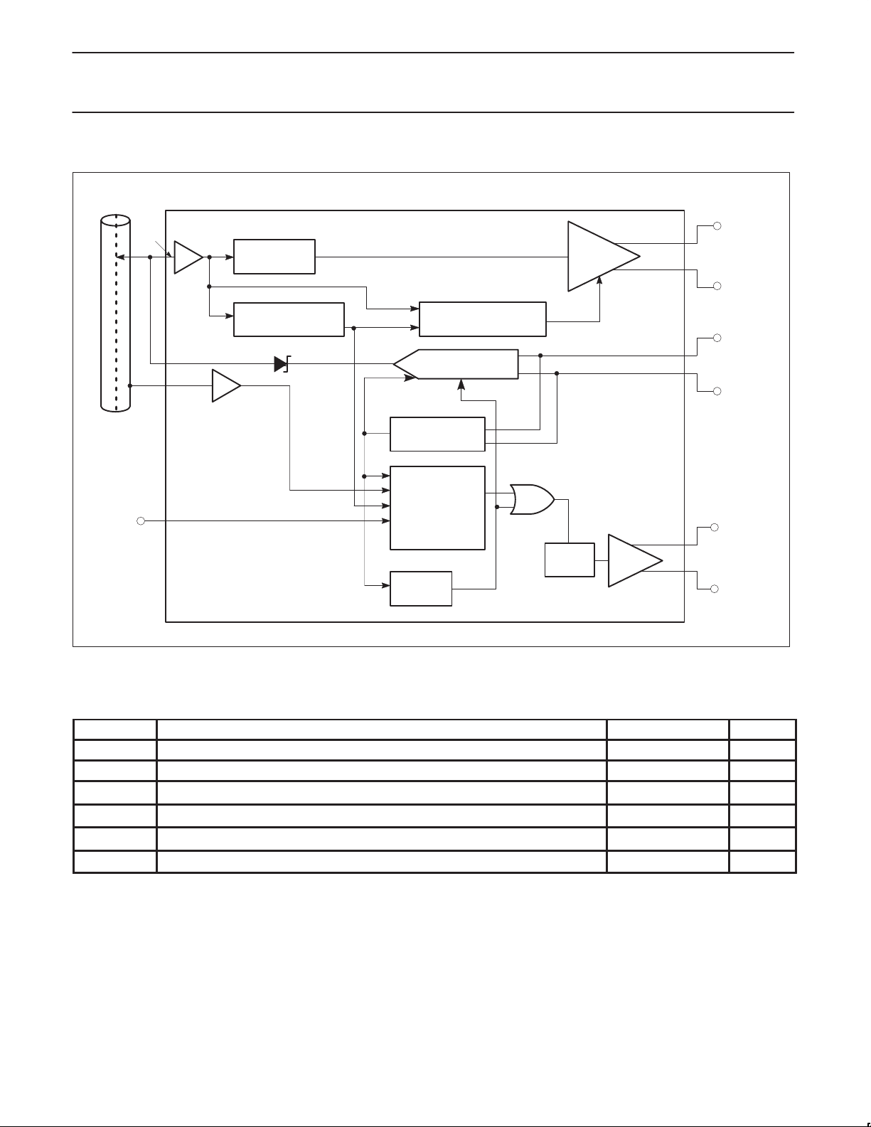
The NE83Q92 is a low power BiCMOS coaxial transceiver interface
(CTI) for Ethernet (10base5) and Thin Ethernet (10base2) local area
networks. The CTI is connected between the coaxial cable and the
Data Terminal Equipment (DTE) and consists of a receiver,
transmitter, receive-mode collision detector, heartbeat generator and
jabber timer (see Block Diagram). The transmitter output connects
directly to a doubly terminated 50Ω cable, while the receiver output,
collision detector output and transmitter input are connected to the
DTE through isolation transformers. Isolation between the CTI and
the DTE is an IEEE 802.3 requirement that can be met on signal
lines by using a set of pulse transformers. Power isolation for the
CTI is achieved using DC-to-DC conversion through a power
transformer (see Figure 3, Connection Diagram).
The part is fully pin compatible with the industry standard 8392, but
has substantially lower current consumption, is fully compliant with
the IEEE802.3 standard, and has additional features such as
optional pull-down resistors (Figure 3, Note 4), and automatic
selection between AUI and coaxial connections.
The NE83Q92 is manufactured on an advanced BiCMOS process
and is available with PLCC and SOL packages which make it ideally
suited to lap-top personal computers or systems where low power
consumption, limited board space and jumperless design is
required. Refer to selection flow chart for optimal apllication.
FEA TURES
•Fully compliant with Ethernet II, IEEE 802.3 10BASE-5 and
10BASE-2, and ISO 8802/3 interface specifications
•100% drop-in compatible with industry standard 8392 sockets
(N & A options)
•Optimal implementation can use 1 Watt DC-DC converter and
reduces external part count by not requiring external pull-down
resistors
•High efficiency AUI drivers automatically power-down under idle
conditions to minimize current consumption
•Automatically disables AUI drivers when no coaxial cable is
connected, allowing hard-wiring of AUI connection and
local/integrated CTI connection
•Smart squelch on data inputs eliminates false activations
•Advanced BiCMOS process for extremely low power operation
•Available in 16-pin DIP, 16-pin SOL and both 20- and 28-pin
PLCC packages
•Expanded version (NE83Q93) with 5 LED status drivers is
available for repeater and advanced system applications
•Full ESD protection
•Power-on reset prevents glitches on coaxial cable
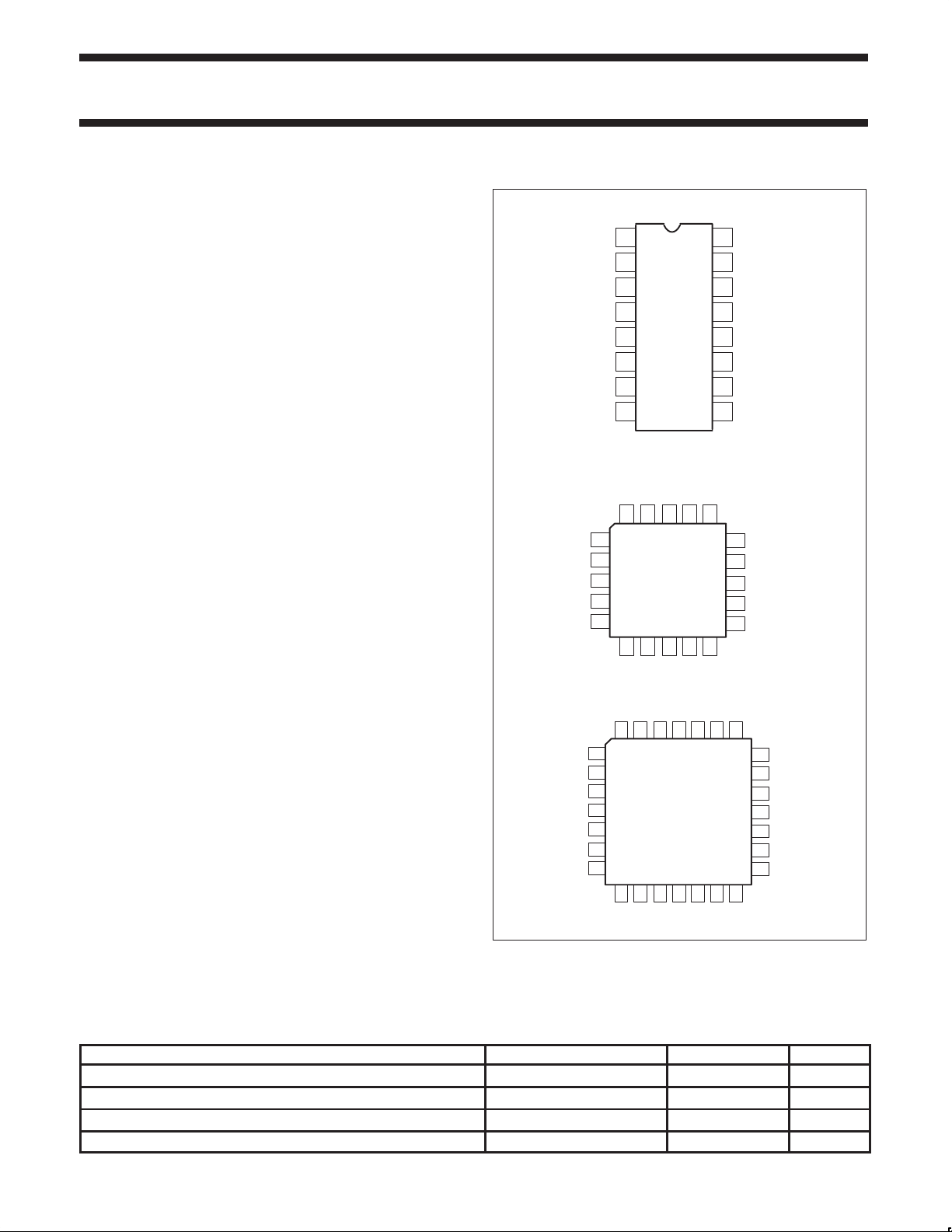
PIN CONFIGURATION
D, N Packages
CD+
1
2
CD–
3
RX+
V
4
EE
V
5
EE
6
RX–
7
TX+
8
TX–
A Packages
CD–
4
RX+
5
V
EE
V
6
EE
V
7
EE
8
RX–
910111213
TX+
RX+
V
5
EE
V
6
EE
V
7
EE
V
8
EE
V
9
EE
V
10
EE
V
11
EE
12 13 14 15 16 17 18
RX–
Figure 1. Pin Configurations
CD+
TX–
CD–
TX+
CD+
TX–
N/C
GND
1234
20123
CDS
HBE
CDS
HBE
19
TXO
GND
16
15
14
13
12
11
10
TXO
GND
N/C
9
18
17
16
15
14
262728
GND
CDS
TXO
RXI
V
EE
RR–
RR+
GND
HBE
RXI
V
EE
V
EE
RR–
RR+
RXI
25
24
23
22
21
20
19
RR+
SD00302
V
EE
V
EE
V
EE
V
EE
V
EE
V
EE
RR–
ORDERING INFORMATION
DESCRIPTION TEMPERATURE RANGE ORDER CODE DWG #
16-Pin Plastic Dual In-Line Package (DIP)
16-Pin Plastic Small Outline Large (SOL) Package
20-Pin Plastic Leaded Chip Carrier (PLCC) Package
28-Pin Plastic Leaded Chip Carrier (PLCC) Package
1995 May 01 853-1737 15180
2
0 to +70°C
0 to +70°C
0 to +70°C
0 to +70°C
NE83Q92N SOT38-4
NE83Q92D SOT162-1
NE83Q92A20 SOT380-1
NE83Q92A SOT261-3
Philips Semiconductors Product specification
NE83Q92Low-power coaxial Ethernet transceiver
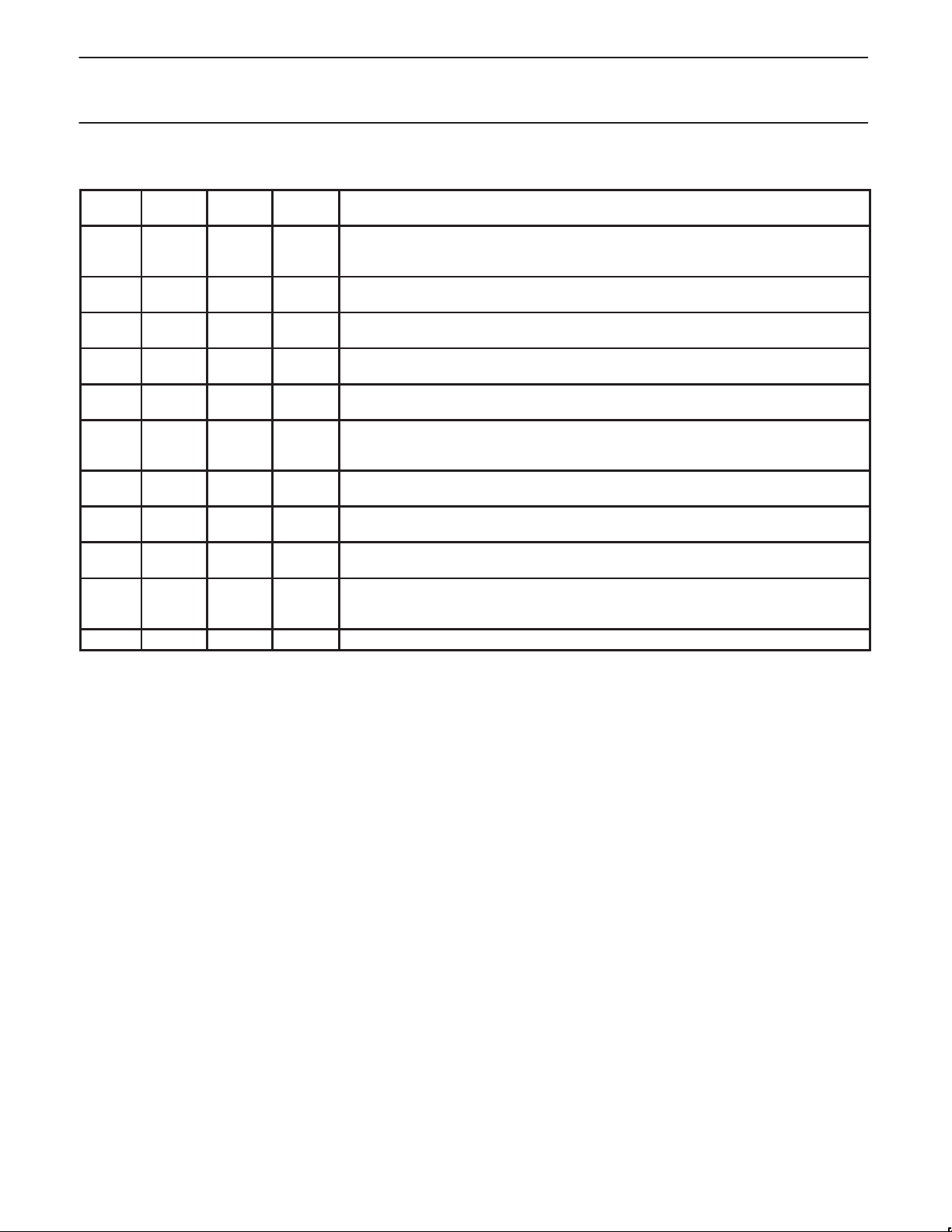
PIN DESCRIPTIONS
PIN NO.
N PKG
PIN NO.
PLCC-20
1
2
3
6
7
8
9 12 15 HBE
11
12
14 18 26 RXI
15 19 28 TXO
16 20 1 CDS
10
4
5
13
10
14
15
11
13
5 – 7
16 – 17
PIN NO.
PLCC-28
2
3
4
8
9
1 N/C Not used.
12
13
14
18
19
16
17
5 to 11
20 to 25 V
SYMBOL DESCRIPTION
2
3
4
CD+
CD–
RX+
RX–
TX+
TX–
RR+
RR–
GND Positive Supply Pin.
EE
Collision Outputs. Balanced differential line driver outputs which send a 10MHz signal to the
DTE in the event of a collision, jabber interrupt or heartbeat test. External pull-down resistors
are optional.
Receiver Outputs. Balanced differential line driver outputs which send the received signal to
the DTE. External pull-down resistors are optional.
Transmitter Inputs. Balanced differential line receiver inputs which accept the transmission
signal from the DTE and apply it to the coaxial cable at TXO, if it meets Tx squelch threshold.
Heartbeat Enable. The heartbeat function is disabled when this pin is connected to VEE and
enabled when connected to GND or left floating.
External Resistor. A 1kΩ (1%) resistor connected between these pins establishes the
signaling current at TXO.
Receiver Input. This pin is connected directly to the coaxial cable. Received signals are
equalized, amplified, and sent to the DTE through the RX± pins, if it meets Rx squelch
threshold.
Transmitter Output. This pin is connected directly (Thin Ethernet) or through an external
isolating diode (Ethernet) to the coaxial cable.
Collision Detect Sense. Ground sense connection for the collision detection circuitry. This
pin should be connected directly to the coaxial cable shield for standard Ethernet operation.
Negative supply pins.
NOTE:
1. The IEEE 802.3 name for CD is CI; for RX is DI; for TX is DO.
1995 May 01
3
Philips Semiconductors Product specification
NE83Q92Low-power coaxial Ethernet transceiver
BLOCK DIAGRAM
COAX
CABLE
DTE
INTERFACE
RXI
BUFFER
EQUALIZER
4–POLE BESSEL
LOW PASS FILTER
TXO
CDS
SENSE
BUFFER
HEARTBEAT ENABLE
RECEIVER
RECEIVER
AC–DC SQUELCH
TRANSMITTER
TRANSMITTER
SQUELCH
COLLISION
COMPARATOR
&
HEARTBEAT
GENERATOR
JABBER
TIMER
Figure 2. Block Diagram
LINE
DRIVER
10MHz
OSC
LINE
DRIVER
RECEIVE
PAIR
(RX+, RX–)
TRANSMIT
PAIR
(TX+, TX–)
COLLISION
PAIR
(CD+, CD–)
SD00274
ABSOLUTE MAXIMUM RATINGS
SYMBOL PARAMETER RATING UNIT
V
V
T
T
T
θ
JA
EE
IN
STG
SOLD
J
Supply voltage
Voltage at any input
Storage temperature range –65 to +150
Lead soldering temperature (10sec.) +300
Recommended max junction temperature
Thermal impedance (N and A packages) 60
NOTE:
1. 100% measured in production.
2. The junction temperature is calculated from the following expression:
T
where
= TA + θ
J
[(VEE x 0.015 x n
JA
TA = Ambient temperature in °C.
θJA = Thermal resistance of package.
V
= Normal operating supply voltage in volts.
EE
= Percentage of duty cycle idle
n
IDL
n
= Percentage of duty cycle receiving
RX
n
= Percentage of duty cycle transmitting
TX
1995 May 01
1
1
2
) + (VEE x 0.027 x nRX) + (VEE x 0.075 x nTX)]
IDL
–12 V
0 to –12 V
+150
4
°C
°C
°C
°C/W
Philips Semiconductors Product specification
NE83Q92Low-power coaxial Ethernet transceiver
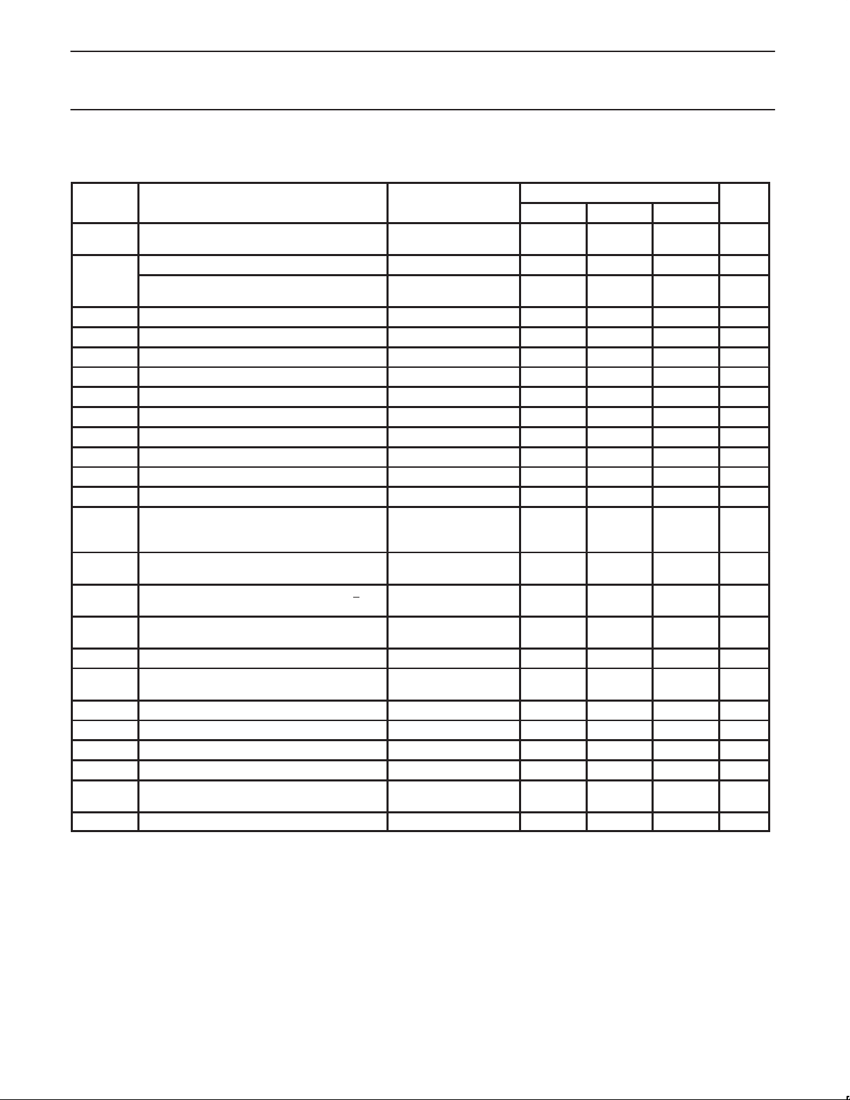
ELECTRICAL CHARACTERISTICS
4
MAX
CD
1,2
. No external isolation
Without external
pull-down resistors
Measured by applying
DC voltage at RXI
Measured as DC
voltage at RXI
V
RXI
TX+
and V
are the max and min voltages at TXO with a 25Ω load between TXO and
MIN
.
LIMITS
–7.5 V
–80 –90 mA
= 0V –2 +25 µA
RXI
= 0V +1 +3 µA
CDS
+2.4 V
EE
+1.6 V
EE
= 0V +10 µA
HBE
HBE
= V
EE
–30 µA
–37 –45 mA
±28 ±I
= –10V –250 +250 µA
TXO
TDC
–3.7 V
–1450 –1530 –1580 mV
(CDS = 0V)
–3.5 V
±600 ±1100 mV
±40 mV
average DC
(CDS = 0V)
– V
) peak –175 –225 –275 mV
TX–
–150 –250 –350 mV
1 2 pF
6 kΩ
mA
VEE = –9V ±6%; TA = 0°C to +70°C unless otherwise specified
SYMBOL PARAMETER TEST CONDITIONS MIN TYP MAX UNIT
V
UVL
Under voltage lockout. Transceiver disabled for
|VEE| < |V
UVL
|
Supply current idle –15 –20 mA
I
I
I
I
I
V
V
V
V
V
V
V
R
C
R
R
EE
I
RXI
CDS
V
IH
V
IL
I
IH
I
IL
TDC
TAC
TX10
TCOM
CD
DIS
OD
OB
OC
RS
V
TS
RXI
RXI
TXO
AUIZ
R
TX
Supply current transmitting (without collision)
Receive input bias current V
Cable sense input bias current V
HBE input HIGH voltage V
HBE input LOW voltage V
HBE input HIGH current V
HBE input LOW current V
Transmit output DC current level
Transmit output AC current level
3
3
Transmit current V
Transmitter output voltage compliance
Collision threshold
5
AUI disable voltage at RXI
Differential output voltage – non idle at RX± and
6
CD±
Differential output voltage imbalance – idle at
RX± and CD±
7
Output common mode voltage at RX± and CD± RXI = 0V –4.0 –5.5 –7.0 V
Receiver squelch threshold
Transmitter squelch threshold (V
Shunt resistance at RXI non–transmitting 100 kΩ
Input capacitance at RXI
8
Shunt resistance at TXO transmitting 7.5 10 kΩ
Differential impedance at RX± and CD± with no
coaxial cable connected
Differential impedance at TX± 20 kΩ
NOTES:
1. Currents flowing into device pins are positive. All voltages are referenced to ground unless otherwise specified. For ease of interpretation,
the parameter limit that appears in the MAX column is the largest value of the parameter, irrespective of sign. Similarly, the value in the MIN
column is the smallest value of the parameter, irrespective of sign.
2. All typical values are for V
3. I
is measured as (V
TDC
GND. I
4. The TXO pin shall continue to sink at least I
is measured as (V
TAC
5. Collision threshold for an AC signal is within 5% of V
= –9V and TA = 27°C.
EE
+ V
MAX
)/(2 x 25) where V
MIN
– V
MAX
MIN
)/(2 x 25).
min when the idle (no signal) voltage on this pin is –3.7V .
TDC
6. Measured on secondary side of isolation transformer (see Connection Diagram, Figure 3). The transformer has a 1:1 turns ratio with an
inductance between 30 and 100µH at 5MHz.
7. Measured as the voltage difference between the RX pins or the CD pins with the transformer removed.
8. Not 100% tested in production.
1995 May 01
5
 Loading...